JP5321840B2 - High voltage bipolar CMOS-DMOS integrated circuit device and modular method for forming the same - Google Patents
High voltage bipolar CMOS-DMOS integrated circuit device and modular method for forming the same Download PDFInfo
- Publication number
- JP5321840B2 JP5321840B2 JP2009513242A JP2009513242A JP5321840B2 JP 5321840 B2 JP5321840 B2 JP 5321840B2 JP 2009513242 A JP2009513242 A JP 2009513242A JP 2009513242 A JP2009513242 A JP 2009513242A JP 5321840 B2 JP5321840 B2 JP 5321840B2
- Authority
- JP
- Japan
- Prior art keywords
- region
- substrate
- well
- gate
- layer
- Prior art date
- Legal status (The legal status is an assumption and is not a legal conclusion. Google has not performed a legal analysis and makes no representation as to the accuracy of the status listed.)
- Expired - Fee Related
Links
- 238000000034 method Methods 0.000 title abstract description 98
- 239000000758 substrate Substances 0.000 claims abstract description 192
- 239000002019 doping agent Substances 0.000 claims abstract description 38
- 239000004065 semiconductor Substances 0.000 claims abstract description 14
- 239000010410 layer Substances 0.000 claims description 342
- 229910052751 metal Inorganic materials 0.000 claims description 89
- 239000002184 metal Substances 0.000 claims description 89
- 238000002955 isolation Methods 0.000 claims description 72
- 229910021420 polycrystalline silicon Inorganic materials 0.000 claims description 40
- 229920005591 polysilicon Polymers 0.000 claims description 40
- 239000011229 interlayer Substances 0.000 claims 9
- 230000008569 process Effects 0.000 abstract description 83
- 238000012545 processing Methods 0.000 abstract description 15
- 238000004519 manufacturing process Methods 0.000 description 75
- 230000015556 catabolic process Effects 0.000 description 67
- 239000007943 implant Substances 0.000 description 55
- 238000002347 injection Methods 0.000 description 51
- 239000007924 injection Substances 0.000 description 51
- 238000002513 implantation Methods 0.000 description 48
- 238000009792 diffusion process Methods 0.000 description 41
- 230000015572 biosynthetic process Effects 0.000 description 40
- 230000005684 electric field Effects 0.000 description 34
- 230000004888 barrier function Effects 0.000 description 32
- 230000000694 effects Effects 0.000 description 27
- 238000000407 epitaxy Methods 0.000 description 21
- 125000006850 spacer group Chemical group 0.000 description 21
- 230000001965 increasing effect Effects 0.000 description 20
- XUIMIQQOPSSXEZ-UHFFFAOYSA-N Silicon Chemical compound [Si] XUIMIQQOPSSXEZ-UHFFFAOYSA-N 0.000 description 18
- 238000013461 design Methods 0.000 description 18
- 229910021332 silicide Inorganic materials 0.000 description 18
- FVBUAEGBCNSCDD-UHFFFAOYSA-N silicide(4-) Chemical compound [Si-4] FVBUAEGBCNSCDD-UHFFFAOYSA-N 0.000 description 18
- 229910052710 silicon Inorganic materials 0.000 description 18
- 239000010703 silicon Substances 0.000 description 18
- ZOXJGFHDIHLPTG-UHFFFAOYSA-N Boron Chemical compound [B] ZOXJGFHDIHLPTG-UHFFFAOYSA-N 0.000 description 17
- 210000000746 body region Anatomy 0.000 description 17
- 235000012431 wafers Nutrition 0.000 description 17
- 229910052796 boron Inorganic materials 0.000 description 16
- 238000005468 ion implantation Methods 0.000 description 16
- 230000008901 benefit Effects 0.000 description 15
- 238000000926 separation method Methods 0.000 description 15
- 230000006870 function Effects 0.000 description 11
- 230000004048 modification Effects 0.000 description 11
- 238000012986 modification Methods 0.000 description 11
- 230000003071 parasitic effect Effects 0.000 description 11
- 229920002120 photoresistant polymer Polymers 0.000 description 11
- 239000002344 surface layer Substances 0.000 description 11
- 230000007423 decrease Effects 0.000 description 10
- 230000007246 mechanism Effects 0.000 description 9
- 238000010586 diagram Methods 0.000 description 7
- 230000005669 field effect Effects 0.000 description 7
- 230000010354 integration Effects 0.000 description 7
- 239000000463 material Substances 0.000 description 7
- 230000002829 reductive effect Effects 0.000 description 7
- TVZRAEYQIKYCPH-UHFFFAOYSA-N 3-(trimethylsilyl)propane-1-sulfonic acid Chemical compound C[Si](C)(C)CCCS(O)(=O)=O TVZRAEYQIKYCPH-UHFFFAOYSA-N 0.000 description 6
- 238000013459 approach Methods 0.000 description 6
- OAICVXFJPJFONN-UHFFFAOYSA-N Phosphorus Chemical compound [P] OAICVXFJPJFONN-UHFFFAOYSA-N 0.000 description 5
- 239000000969 carrier Substances 0.000 description 5
- 230000008859 change Effects 0.000 description 5
- 229910052698 phosphorus Inorganic materials 0.000 description 5
- 239000011574 phosphorus Substances 0.000 description 5
- 230000002441 reversible effect Effects 0.000 description 5
- 239000008186 active pharmaceutical agent Substances 0.000 description 4
- 230000002411 adverse Effects 0.000 description 4
- 230000009471 action Effects 0.000 description 3
- 229910052787 antimony Inorganic materials 0.000 description 3
- WATWJIUSRGPENY-UHFFFAOYSA-N antimony atom Chemical compound [Sb] WATWJIUSRGPENY-UHFFFAOYSA-N 0.000 description 3
- 150000001638 boron Chemical class 0.000 description 3
- 239000013078 crystal Substances 0.000 description 3
- 230000006378 damage Effects 0.000 description 3
- 238000000151 deposition Methods 0.000 description 3
- 230000008021 deposition Effects 0.000 description 3
- 230000000670 limiting effect Effects 0.000 description 3
- 238000001465 metallisation Methods 0.000 description 3
- 230000007704 transition Effects 0.000 description 3
- 241000293849 Cordylanthus Species 0.000 description 2
- 230000000779 depleting effect Effects 0.000 description 2
- 238000009826 distribution Methods 0.000 description 2
- 230000000977 initiatory effect Effects 0.000 description 2
- 238000012423 maintenance Methods 0.000 description 2
- 230000003647 oxidation Effects 0.000 description 2
- 238000007254 oxidation reaction Methods 0.000 description 2
- 206010035148 Plague Diseases 0.000 description 1
- 241000607479 Yersinia pestis Species 0.000 description 1
- 230000002378 acidificating effect Effects 0.000 description 1
- 230000004913 activation Effects 0.000 description 1
- 230000006978 adaptation Effects 0.000 description 1
- 229910052785 arsenic Inorganic materials 0.000 description 1
- RQNWIZPPADIBDY-UHFFFAOYSA-N arsenic atom Chemical compound [As] RQNWIZPPADIBDY-UHFFFAOYSA-N 0.000 description 1
- 238000005513 bias potential Methods 0.000 description 1
- 230000007547 defect Effects 0.000 description 1
- 230000000593 degrading effect Effects 0.000 description 1
- 239000003989 dielectric material Substances 0.000 description 1
- 238000006073 displacement reaction Methods 0.000 description 1
- 230000002708 enhancing effect Effects 0.000 description 1
- 238000005530 etching Methods 0.000 description 1
- 230000007717 exclusion Effects 0.000 description 1
- 238000010438 heat treatment Methods 0.000 description 1
- BHEPBYXIRTUNPN-UHFFFAOYSA-N hydridophosphorus(.) (triplet) Chemical compound [PH] BHEPBYXIRTUNPN-UHFFFAOYSA-N 0.000 description 1
- 238000011065 in-situ storage Methods 0.000 description 1
- 150000002500 ions Chemical class 0.000 description 1
- 238000005304 joining Methods 0.000 description 1
- 229910044991 metal oxide Inorganic materials 0.000 description 1
- 150000004706 metal oxides Chemical class 0.000 description 1
- 229930014626 natural product Natural products 0.000 description 1
- 238000010943 off-gassing Methods 0.000 description 1
- 238000005457 optimization Methods 0.000 description 1
- 230000010355 oscillation Effects 0.000 description 1
- 238000002161 passivation Methods 0.000 description 1
- 230000035515 penetration Effects 0.000 description 1
- 150000003017 phosphorus Chemical class 0.000 description 1
- 230000002265 prevention Effects 0.000 description 1
- 238000004151 rapid thermal annealing Methods 0.000 description 1
- 230000009467 reduction Effects 0.000 description 1
- 230000004044 response Effects 0.000 description 1
- 230000007480 spreading Effects 0.000 description 1
- 238000003892 spreading Methods 0.000 description 1
- 230000003068 static effect Effects 0.000 description 1
- 230000004083 survival effect Effects 0.000 description 1
- WFKWXMTUELFFGS-UHFFFAOYSA-N tungsten Chemical compound [W] WFKWXMTUELFFGS-UHFFFAOYSA-N 0.000 description 1
- 229910052721 tungsten Inorganic materials 0.000 description 1
- 239000010937 tungsten Substances 0.000 description 1
- 230000005641 tunneling Effects 0.000 description 1
Images


Classifications
-
- H—ELECTRICITY
- H01—ELECTRIC ELEMENTS
- H01L—SEMICONDUCTOR DEVICES NOT COVERED BY CLASS H10
- H01L29/00—Semiconductor devices specially adapted for rectifying, amplifying, oscillating or switching and having potential barriers; Capacitors or resistors having potential barriers, e.g. a PN-junction depletion layer or carrier concentration layer; Details of semiconductor bodies or of electrodes thereof ; Multistep manufacturing processes therefor
- H01L29/02—Semiconductor bodies ; Multistep manufacturing processes therefor
- H01L29/06—Semiconductor bodies ; Multistep manufacturing processes therefor characterised by their shape; characterised by the shapes, relative sizes, or dispositions of the semiconductor regions ; characterised by the concentration or distribution of impurities within semiconductor regions
- H01L29/08—Semiconductor bodies ; Multistep manufacturing processes therefor characterised by their shape; characterised by the shapes, relative sizes, or dispositions of the semiconductor regions ; characterised by the concentration or distribution of impurities within semiconductor regions with semiconductor regions connected to an electrode carrying current to be rectified, amplified or switched and such electrode being part of a semiconductor device which comprises three or more electrodes
- H01L29/0843—Source or drain regions of field-effect devices
- H01L29/0847—Source or drain regions of field-effect devices of field-effect transistors with insulated gate
-
- H—ELECTRICITY
- H01—ELECTRIC ELEMENTS
- H01L—SEMICONDUCTOR DEVICES NOT COVERED BY CLASS H10
- H01L21/00—Processes or apparatus adapted for the manufacture or treatment of semiconductor or solid state devices or of parts thereof
- H01L21/70—Manufacture or treatment of devices consisting of a plurality of solid state components formed in or on a common substrate or of parts thereof; Manufacture of integrated circuit devices or of parts thereof
- H01L21/71—Manufacture of specific parts of devices defined in group H01L21/70
- H01L21/76—Making of isolation regions between components
- H01L21/761—PN junctions
-
- H—ELECTRICITY
- H01—ELECTRIC ELEMENTS
- H01L—SEMICONDUCTOR DEVICES NOT COVERED BY CLASS H10
- H01L21/00—Processes or apparatus adapted for the manufacture or treatment of semiconductor or solid state devices or of parts thereof
- H01L21/70—Manufacture or treatment of devices consisting of a plurality of solid state components formed in or on a common substrate or of parts thereof; Manufacture of integrated circuit devices or of parts thereof
- H01L21/77—Manufacture or treatment of devices consisting of a plurality of solid state components or integrated circuits formed in, or on, a common substrate
- H01L21/78—Manufacture or treatment of devices consisting of a plurality of solid state components or integrated circuits formed in, or on, a common substrate with subsequent division of the substrate into plural individual devices
- H01L21/82—Manufacture or treatment of devices consisting of a plurality of solid state components or integrated circuits formed in, or on, a common substrate with subsequent division of the substrate into plural individual devices to produce devices, e.g. integrated circuits, each consisting of a plurality of components
- H01L21/822—Manufacture or treatment of devices consisting of a plurality of solid state components or integrated circuits formed in, or on, a common substrate with subsequent division of the substrate into plural individual devices to produce devices, e.g. integrated circuits, each consisting of a plurality of components the substrate being a semiconductor, using silicon technology
- H01L21/8232—Field-effect technology
- H01L21/8234—MIS technology, i.e. integration processes of field effect transistors of the conductor-insulator-semiconductor type
- H01L21/823462—MIS technology, i.e. integration processes of field effect transistors of the conductor-insulator-semiconductor type with a particular manufacturing method of the gate insulating layers, e.g. different gate insulating layer thicknesses, particular gate insulator materials or particular gate insulator implants
-
- H—ELECTRICITY
- H01—ELECTRIC ELEMENTS
- H01L—SEMICONDUCTOR DEVICES NOT COVERED BY CLASS H10
- H01L21/00—Processes or apparatus adapted for the manufacture or treatment of semiconductor or solid state devices or of parts thereof
- H01L21/70—Manufacture or treatment of devices consisting of a plurality of solid state components formed in or on a common substrate or of parts thereof; Manufacture of integrated circuit devices or of parts thereof
- H01L21/77—Manufacture or treatment of devices consisting of a plurality of solid state components or integrated circuits formed in, or on, a common substrate
- H01L21/78—Manufacture or treatment of devices consisting of a plurality of solid state components or integrated circuits formed in, or on, a common substrate with subsequent division of the substrate into plural individual devices
- H01L21/82—Manufacture or treatment of devices consisting of a plurality of solid state components or integrated circuits formed in, or on, a common substrate with subsequent division of the substrate into plural individual devices to produce devices, e.g. integrated circuits, each consisting of a plurality of components
- H01L21/822—Manufacture or treatment of devices consisting of a plurality of solid state components or integrated circuits formed in, or on, a common substrate with subsequent division of the substrate into plural individual devices to produce devices, e.g. integrated circuits, each consisting of a plurality of components the substrate being a semiconductor, using silicon technology
- H01L21/8232—Field-effect technology
- H01L21/8234—MIS technology, i.e. integration processes of field effect transistors of the conductor-insulator-semiconductor type
- H01L21/823481—MIS technology, i.e. integration processes of field effect transistors of the conductor-insulator-semiconductor type isolation region manufacturing related aspects, e.g. to avoid interaction of isolation region with adjacent structure
-
- H—ELECTRICITY
- H01—ELECTRIC ELEMENTS
- H01L—SEMICONDUCTOR DEVICES NOT COVERED BY CLASS H10
- H01L21/00—Processes or apparatus adapted for the manufacture or treatment of semiconductor or solid state devices or of parts thereof
- H01L21/70—Manufacture or treatment of devices consisting of a plurality of solid state components formed in or on a common substrate or of parts thereof; Manufacture of integrated circuit devices or of parts thereof
- H01L21/77—Manufacture or treatment of devices consisting of a plurality of solid state components or integrated circuits formed in, or on, a common substrate
- H01L21/78—Manufacture or treatment of devices consisting of a plurality of solid state components or integrated circuits formed in, or on, a common substrate with subsequent division of the substrate into plural individual devices
- H01L21/82—Manufacture or treatment of devices consisting of a plurality of solid state components or integrated circuits formed in, or on, a common substrate with subsequent division of the substrate into plural individual devices to produce devices, e.g. integrated circuits, each consisting of a plurality of components
- H01L21/822—Manufacture or treatment of devices consisting of a plurality of solid state components or integrated circuits formed in, or on, a common substrate with subsequent division of the substrate into plural individual devices to produce devices, e.g. integrated circuits, each consisting of a plurality of components the substrate being a semiconductor, using silicon technology
- H01L21/8232—Field-effect technology
- H01L21/8234—MIS technology, i.e. integration processes of field effect transistors of the conductor-insulator-semiconductor type
- H01L21/823493—MIS technology, i.e. integration processes of field effect transistors of the conductor-insulator-semiconductor type with a particular manufacturing method of the wells or tubs, e.g. twin tubs, high energy well implants, buried implanted layers for lateral isolation [BILLI]
-
- H—ELECTRICITY
- H01—ELECTRIC ELEMENTS
- H01L—SEMICONDUCTOR DEVICES NOT COVERED BY CLASS H10
- H01L21/00—Processes or apparatus adapted for the manufacture or treatment of semiconductor or solid state devices or of parts thereof
- H01L21/70—Manufacture or treatment of devices consisting of a plurality of solid state components formed in or on a common substrate or of parts thereof; Manufacture of integrated circuit devices or of parts thereof
- H01L21/77—Manufacture or treatment of devices consisting of a plurality of solid state components or integrated circuits formed in, or on, a common substrate
- H01L21/78—Manufacture or treatment of devices consisting of a plurality of solid state components or integrated circuits formed in, or on, a common substrate with subsequent division of the substrate into plural individual devices
- H01L21/82—Manufacture or treatment of devices consisting of a plurality of solid state components or integrated circuits formed in, or on, a common substrate with subsequent division of the substrate into plural individual devices to produce devices, e.g. integrated circuits, each consisting of a plurality of components
- H01L21/822—Manufacture or treatment of devices consisting of a plurality of solid state components or integrated circuits formed in, or on, a common substrate with subsequent division of the substrate into plural individual devices to produce devices, e.g. integrated circuits, each consisting of a plurality of components the substrate being a semiconductor, using silicon technology
- H01L21/8248—Combination of bipolar and field-effect technology
- H01L21/8249—Bipolar and MOS technology
-
- H—ELECTRICITY
- H01—ELECTRIC ELEMENTS
- H01L—SEMICONDUCTOR DEVICES NOT COVERED BY CLASS H10
- H01L27/00—Devices consisting of a plurality of semiconductor or other solid-state components formed in or on a common substrate
- H01L27/02—Devices consisting of a plurality of semiconductor or other solid-state components formed in or on a common substrate including semiconductor components specially adapted for rectifying, oscillating, amplifying or switching and having potential barriers; including integrated passive circuit elements having potential barriers
- H01L27/04—Devices consisting of a plurality of semiconductor or other solid-state components formed in or on a common substrate including semiconductor components specially adapted for rectifying, oscillating, amplifying or switching and having potential barriers; including integrated passive circuit elements having potential barriers the substrate being a semiconductor body
- H01L27/06—Devices consisting of a plurality of semiconductor or other solid-state components formed in or on a common substrate including semiconductor components specially adapted for rectifying, oscillating, amplifying or switching and having potential barriers; including integrated passive circuit elements having potential barriers the substrate being a semiconductor body including a plurality of individual components in a non-repetitive configuration
- H01L27/0611—Devices consisting of a plurality of semiconductor or other solid-state components formed in or on a common substrate including semiconductor components specially adapted for rectifying, oscillating, amplifying or switching and having potential barriers; including integrated passive circuit elements having potential barriers the substrate being a semiconductor body including a plurality of individual components in a non-repetitive configuration integrated circuits having a two-dimensional layout of components without a common active region
- H01L27/0617—Devices consisting of a plurality of semiconductor or other solid-state components formed in or on a common substrate including semiconductor components specially adapted for rectifying, oscillating, amplifying or switching and having potential barriers; including integrated passive circuit elements having potential barriers the substrate being a semiconductor body including a plurality of individual components in a non-repetitive configuration integrated circuits having a two-dimensional layout of components without a common active region comprising components of the field-effect type
- H01L27/0623—Devices consisting of a plurality of semiconductor or other solid-state components formed in or on a common substrate including semiconductor components specially adapted for rectifying, oscillating, amplifying or switching and having potential barriers; including integrated passive circuit elements having potential barriers the substrate being a semiconductor body including a plurality of individual components in a non-repetitive configuration integrated circuits having a two-dimensional layout of components without a common active region comprising components of the field-effect type in combination with bipolar transistors
-
- H—ELECTRICITY
- H01—ELECTRIC ELEMENTS
- H01L—SEMICONDUCTOR DEVICES NOT COVERED BY CLASS H10
- H01L27/00—Devices consisting of a plurality of semiconductor or other solid-state components formed in or on a common substrate
- H01L27/02—Devices consisting of a plurality of semiconductor or other solid-state components formed in or on a common substrate including semiconductor components specially adapted for rectifying, oscillating, amplifying or switching and having potential barriers; including integrated passive circuit elements having potential barriers
- H01L27/04—Devices consisting of a plurality of semiconductor or other solid-state components formed in or on a common substrate including semiconductor components specially adapted for rectifying, oscillating, amplifying or switching and having potential barriers; including integrated passive circuit elements having potential barriers the substrate being a semiconductor body
- H01L27/08—Devices consisting of a plurality of semiconductor or other solid-state components formed in or on a common substrate including semiconductor components specially adapted for rectifying, oscillating, amplifying or switching and having potential barriers; including integrated passive circuit elements having potential barriers the substrate being a semiconductor body including only semiconductor components of a single kind
- H01L27/085—Devices consisting of a plurality of semiconductor or other solid-state components formed in or on a common substrate including semiconductor components specially adapted for rectifying, oscillating, amplifying or switching and having potential barriers; including integrated passive circuit elements having potential barriers the substrate being a semiconductor body including only semiconductor components of a single kind including field-effect components only
- H01L27/088—Devices consisting of a plurality of semiconductor or other solid-state components formed in or on a common substrate including semiconductor components specially adapted for rectifying, oscillating, amplifying or switching and having potential barriers; including integrated passive circuit elements having potential barriers the substrate being a semiconductor body including only semiconductor components of a single kind including field-effect components only the components being field-effect transistors with insulated gate
-
- H—ELECTRICITY
- H01—ELECTRIC ELEMENTS
- H01L—SEMICONDUCTOR DEVICES NOT COVERED BY CLASS H10
- H01L27/00—Devices consisting of a plurality of semiconductor or other solid-state components formed in or on a common substrate
- H01L27/02—Devices consisting of a plurality of semiconductor or other solid-state components formed in or on a common substrate including semiconductor components specially adapted for rectifying, oscillating, amplifying or switching and having potential barriers; including integrated passive circuit elements having potential barriers
- H01L27/04—Devices consisting of a plurality of semiconductor or other solid-state components formed in or on a common substrate including semiconductor components specially adapted for rectifying, oscillating, amplifying or switching and having potential barriers; including integrated passive circuit elements having potential barriers the substrate being a semiconductor body
- H01L27/08—Devices consisting of a plurality of semiconductor or other solid-state components formed in or on a common substrate including semiconductor components specially adapted for rectifying, oscillating, amplifying or switching and having potential barriers; including integrated passive circuit elements having potential barriers the substrate being a semiconductor body including only semiconductor components of a single kind
- H01L27/085—Devices consisting of a plurality of semiconductor or other solid-state components formed in or on a common substrate including semiconductor components specially adapted for rectifying, oscillating, amplifying or switching and having potential barriers; including integrated passive circuit elements having potential barriers the substrate being a semiconductor body including only semiconductor components of a single kind including field-effect components only
- H01L27/098—Devices consisting of a plurality of semiconductor or other solid-state components formed in or on a common substrate including semiconductor components specially adapted for rectifying, oscillating, amplifying or switching and having potential barriers; including integrated passive circuit elements having potential barriers the substrate being a semiconductor body including only semiconductor components of a single kind including field-effect components only the components being PN junction gate field-effect transistors
-
- H—ELECTRICITY
- H01—ELECTRIC ELEMENTS
- H01L—SEMICONDUCTOR DEVICES NOT COVERED BY CLASS H10
- H01L29/00—Semiconductor devices specially adapted for rectifying, amplifying, oscillating or switching and having potential barriers; Capacitors or resistors having potential barriers, e.g. a PN-junction depletion layer or carrier concentration layer; Details of semiconductor bodies or of electrodes thereof ; Multistep manufacturing processes therefor
- H01L29/02—Semiconductor bodies ; Multistep manufacturing processes therefor
- H01L29/06—Semiconductor bodies ; Multistep manufacturing processes therefor characterised by their shape; characterised by the shapes, relative sizes, or dispositions of the semiconductor regions ; characterised by the concentration or distribution of impurities within semiconductor regions
- H01L29/08—Semiconductor bodies ; Multistep manufacturing processes therefor characterised by their shape; characterised by the shapes, relative sizes, or dispositions of the semiconductor regions ; characterised by the concentration or distribution of impurities within semiconductor regions with semiconductor regions connected to an electrode carrying current to be rectified, amplified or switched and such electrode being part of a semiconductor device which comprises three or more electrodes
- H01L29/0843—Source or drain regions of field-effect devices
- H01L29/0847—Source or drain regions of field-effect devices of field-effect transistors with insulated gate
- H01L29/0852—Source or drain regions of field-effect devices of field-effect transistors with insulated gate of DMOS transistors
- H01L29/0873—Drain regions
- H01L29/0878—Impurity concentration or distribution
-
- H—ELECTRICITY
- H01—ELECTRIC ELEMENTS
- H01L—SEMICONDUCTOR DEVICES NOT COVERED BY CLASS H10
- H01L29/00—Semiconductor devices specially adapted for rectifying, amplifying, oscillating or switching and having potential barriers; Capacitors or resistors having potential barriers, e.g. a PN-junction depletion layer or carrier concentration layer; Details of semiconductor bodies or of electrodes thereof ; Multistep manufacturing processes therefor
- H01L29/40—Electrodes ; Multistep manufacturing processes therefor
- H01L29/41—Electrodes ; Multistep manufacturing processes therefor characterised by their shape, relative sizes or dispositions
- H01L29/423—Electrodes ; Multistep manufacturing processes therefor characterised by their shape, relative sizes or dispositions not carrying the current to be rectified, amplified or switched
- H01L29/42312—Gate electrodes for field effect devices
- H01L29/42316—Gate electrodes for field effect devices for field-effect transistors
- H01L29/4232—Gate electrodes for field effect devices for field-effect transistors with insulated gate
- H01L29/42364—Gate electrodes for field effect devices for field-effect transistors with insulated gate characterised by the insulating layer, e.g. thickness or uniformity
- H01L29/42368—Gate electrodes for field effect devices for field-effect transistors with insulated gate characterised by the insulating layer, e.g. thickness or uniformity the thickness being non-uniform
-
- H—ELECTRICITY
- H01—ELECTRIC ELEMENTS
- H01L—SEMICONDUCTOR DEVICES NOT COVERED BY CLASS H10
- H01L29/00—Semiconductor devices specially adapted for rectifying, amplifying, oscillating or switching and having potential barriers; Capacitors or resistors having potential barriers, e.g. a PN-junction depletion layer or carrier concentration layer; Details of semiconductor bodies or of electrodes thereof ; Multistep manufacturing processes therefor
- H01L29/66—Types of semiconductor device ; Multistep manufacturing processes therefor
- H01L29/66007—Multistep manufacturing processes
- H01L29/66075—Multistep manufacturing processes of devices having semiconductor bodies comprising group 14 or group 13/15 materials
- H01L29/66083—Multistep manufacturing processes of devices having semiconductor bodies comprising group 14 or group 13/15 materials the devices being controllable only by variation of the electric current supplied or the electric potential applied, to one or more of the electrodes carrying the current to be rectified, amplified, oscillated or switched, e.g. two-terminal devices
- H01L29/6609—Diodes
- H01L29/66098—Breakdown diodes
- H01L29/66106—Zener diodes
-
- H—ELECTRICITY
- H01—ELECTRIC ELEMENTS
- H01L—SEMICONDUCTOR DEVICES NOT COVERED BY CLASS H10
- H01L29/00—Semiconductor devices specially adapted for rectifying, amplifying, oscillating or switching and having potential barriers; Capacitors or resistors having potential barriers, e.g. a PN-junction depletion layer or carrier concentration layer; Details of semiconductor bodies or of electrodes thereof ; Multistep manufacturing processes therefor
- H01L29/66—Types of semiconductor device ; Multistep manufacturing processes therefor
- H01L29/66007—Multistep manufacturing processes
- H01L29/66075—Multistep manufacturing processes of devices having semiconductor bodies comprising group 14 or group 13/15 materials
- H01L29/66227—Multistep manufacturing processes of devices having semiconductor bodies comprising group 14 or group 13/15 materials the devices being controllable only by the electric current supplied or the electric potential applied, to an electrode which does not carry the current to be rectified, amplified or switched, e.g. three-terminal devices
- H01L29/66409—Unipolar field-effect transistors
- H01L29/66477—Unipolar field-effect transistors with an insulated gate, i.e. MISFET
- H01L29/66568—Lateral single gate silicon transistors
- H01L29/66659—Lateral single gate silicon transistors with asymmetry in the channel direction, e.g. lateral high-voltage MISFETs with drain offset region, extended drain MISFETs
-
- H—ELECTRICITY
- H01—ELECTRIC ELEMENTS
- H01L—SEMICONDUCTOR DEVICES NOT COVERED BY CLASS H10
- H01L29/00—Semiconductor devices specially adapted for rectifying, amplifying, oscillating or switching and having potential barriers; Capacitors or resistors having potential barriers, e.g. a PN-junction depletion layer or carrier concentration layer; Details of semiconductor bodies or of electrodes thereof ; Multistep manufacturing processes therefor
- H01L29/66—Types of semiconductor device ; Multistep manufacturing processes therefor
- H01L29/66007—Multistep manufacturing processes
- H01L29/66075—Multistep manufacturing processes of devices having semiconductor bodies comprising group 14 or group 13/15 materials
- H01L29/66227—Multistep manufacturing processes of devices having semiconductor bodies comprising group 14 or group 13/15 materials the devices being controllable only by the electric current supplied or the electric potential applied, to an electrode which does not carry the current to be rectified, amplified or switched, e.g. three-terminal devices
- H01L29/66409—Unipolar field-effect transistors
- H01L29/66477—Unipolar field-effect transistors with an insulated gate, i.e. MISFET
- H01L29/66674—DMOS transistors, i.e. MISFETs with a channel accommodating body or base region adjoining a drain drift region
- H01L29/66681—Lateral DMOS transistors, i.e. LDMOS transistors
- H01L29/66704—Lateral DMOS transistors, i.e. LDMOS transistors with a step of recessing the gate electrode, e.g. to form a trench gate electrode
-
- H—ELECTRICITY
- H01—ELECTRIC ELEMENTS
- H01L—SEMICONDUCTOR DEVICES NOT COVERED BY CLASS H10
- H01L29/00—Semiconductor devices specially adapted for rectifying, amplifying, oscillating or switching and having potential barriers; Capacitors or resistors having potential barriers, e.g. a PN-junction depletion layer or carrier concentration layer; Details of semiconductor bodies or of electrodes thereof ; Multistep manufacturing processes therefor
- H01L29/66—Types of semiconductor device ; Multistep manufacturing processes therefor
- H01L29/66007—Multistep manufacturing processes
- H01L29/66075—Multistep manufacturing processes of devices having semiconductor bodies comprising group 14 or group 13/15 materials
- H01L29/66227—Multistep manufacturing processes of devices having semiconductor bodies comprising group 14 or group 13/15 materials the devices being controllable only by the electric current supplied or the electric potential applied, to an electrode which does not carry the current to be rectified, amplified or switched, e.g. three-terminal devices
- H01L29/66409—Unipolar field-effect transistors
- H01L29/66893—Unipolar field-effect transistors with a PN junction gate, i.e. JFET
- H01L29/66901—Unipolar field-effect transistors with a PN junction gate, i.e. JFET with a PN homojunction gate
-
- H—ELECTRICITY
- H01—ELECTRIC ELEMENTS
- H01L—SEMICONDUCTOR DEVICES NOT COVERED BY CLASS H10
- H01L29/00—Semiconductor devices specially adapted for rectifying, amplifying, oscillating or switching and having potential barriers; Capacitors or resistors having potential barriers, e.g. a PN-junction depletion layer or carrier concentration layer; Details of semiconductor bodies or of electrodes thereof ; Multistep manufacturing processes therefor
- H01L29/66—Types of semiconductor device ; Multistep manufacturing processes therefor
- H01L29/68—Types of semiconductor device ; Multistep manufacturing processes therefor controllable by only the electric current supplied, or only the electric potential applied, to an electrode which does not carry the current to be rectified, amplified or switched
- H01L29/76—Unipolar devices, e.g. field effect transistors
- H01L29/772—Field effect transistors
- H01L29/78—Field effect transistors with field effect produced by an insulated gate
- H01L29/7801—DMOS transistors, i.e. MISFETs with a channel accommodating body or base region adjoining a drain drift region
- H01L29/7816—Lateral DMOS transistors, i.e. LDMOS transistors
- H01L29/7825—Lateral DMOS transistors, i.e. LDMOS transistors with trench gate electrode
-
- H—ELECTRICITY
- H01—ELECTRIC ELEMENTS
- H01L—SEMICONDUCTOR DEVICES NOT COVERED BY CLASS H10
- H01L29/00—Semiconductor devices specially adapted for rectifying, amplifying, oscillating or switching and having potential barriers; Capacitors or resistors having potential barriers, e.g. a PN-junction depletion layer or carrier concentration layer; Details of semiconductor bodies or of electrodes thereof ; Multistep manufacturing processes therefor
- H01L29/66—Types of semiconductor device ; Multistep manufacturing processes therefor
- H01L29/68—Types of semiconductor device ; Multistep manufacturing processes therefor controllable by only the electric current supplied, or only the electric potential applied, to an electrode which does not carry the current to be rectified, amplified or switched
- H01L29/76—Unipolar devices, e.g. field effect transistors
- H01L29/772—Field effect transistors
- H01L29/78—Field effect transistors with field effect produced by an insulated gate
- H01L29/7833—Field effect transistors with field effect produced by an insulated gate with lightly doped drain or source extension, e.g. LDD MOSFET's; DDD MOSFET's
- H01L29/7835—Field effect transistors with field effect produced by an insulated gate with lightly doped drain or source extension, e.g. LDD MOSFET's; DDD MOSFET's with asymmetrical source and drain regions, e.g. lateral high-voltage MISFETs with drain offset region, extended drain MISFETs
-
- H—ELECTRICITY
- H01—ELECTRIC ELEMENTS
- H01L—SEMICONDUCTOR DEVICES NOT COVERED BY CLASS H10
- H01L29/00—Semiconductor devices specially adapted for rectifying, amplifying, oscillating or switching and having potential barriers; Capacitors or resistors having potential barriers, e.g. a PN-junction depletion layer or carrier concentration layer; Details of semiconductor bodies or of electrodes thereof ; Multistep manufacturing processes therefor
- H01L29/66—Types of semiconductor device ; Multistep manufacturing processes therefor
- H01L29/68—Types of semiconductor device ; Multistep manufacturing processes therefor controllable by only the electric current supplied, or only the electric potential applied, to an electrode which does not carry the current to be rectified, amplified or switched
- H01L29/76—Unipolar devices, e.g. field effect transistors
- H01L29/772—Field effect transistors
- H01L29/80—Field effect transistors with field effect produced by a PN or other rectifying junction gate, i.e. potential-jump barrier
- H01L29/808—Field effect transistors with field effect produced by a PN or other rectifying junction gate, i.e. potential-jump barrier with a PN junction gate, e.g. PN homojunction gate
-
- H—ELECTRICITY
- H01—ELECTRIC ELEMENTS
- H01L—SEMICONDUCTOR DEVICES NOT COVERED BY CLASS H10
- H01L29/00—Semiconductor devices specially adapted for rectifying, amplifying, oscillating or switching and having potential barriers; Capacitors or resistors having potential barriers, e.g. a PN-junction depletion layer or carrier concentration layer; Details of semiconductor bodies or of electrodes thereof ; Multistep manufacturing processes therefor
- H01L29/66—Types of semiconductor device ; Multistep manufacturing processes therefor
- H01L29/86—Types of semiconductor device ; Multistep manufacturing processes therefor controllable only by variation of the electric current supplied, or only the electric potential applied, to one or more of the electrodes carrying the current to be rectified, amplified, oscillated or switched
- H01L29/861—Diodes
- H01L29/866—Zener diodes
-
- H—ELECTRICITY
- H01—ELECTRIC ELEMENTS
- H01L—SEMICONDUCTOR DEVICES NOT COVERED BY CLASS H10
- H01L29/00—Semiconductor devices specially adapted for rectifying, amplifying, oscillating or switching and having potential barriers; Capacitors or resistors having potential barriers, e.g. a PN-junction depletion layer or carrier concentration layer; Details of semiconductor bodies or of electrodes thereof ; Multistep manufacturing processes therefor
- H01L29/02—Semiconductor bodies ; Multistep manufacturing processes therefor
- H01L29/06—Semiconductor bodies ; Multistep manufacturing processes therefor characterised by their shape; characterised by the shapes, relative sizes, or dispositions of the semiconductor regions ; characterised by the concentration or distribution of impurities within semiconductor regions
- H01L29/0684—Semiconductor bodies ; Multistep manufacturing processes therefor characterised by their shape; characterised by the shapes, relative sizes, or dispositions of the semiconductor regions ; characterised by the concentration or distribution of impurities within semiconductor regions characterised by the shape, relative sizes or dispositions of the semiconductor regions or junctions between the regions
- H01L29/0692—Surface layout
- H01L29/0696—Surface layout of cellular field-effect devices, e.g. multicellular DMOS transistors or IGBTs
-
- H—ELECTRICITY
- H01—ELECTRIC ELEMENTS
- H01L—SEMICONDUCTOR DEVICES NOT COVERED BY CLASS H10
- H01L29/00—Semiconductor devices specially adapted for rectifying, amplifying, oscillating or switching and having potential barriers; Capacitors or resistors having potential barriers, e.g. a PN-junction depletion layer or carrier concentration layer; Details of semiconductor bodies or of electrodes thereof ; Multistep manufacturing processes therefor
- H01L29/02—Semiconductor bodies ; Multistep manufacturing processes therefor
- H01L29/06—Semiconductor bodies ; Multistep manufacturing processes therefor characterised by their shape; characterised by the shapes, relative sizes, or dispositions of the semiconductor regions ; characterised by the concentration or distribution of impurities within semiconductor regions
- H01L29/08—Semiconductor bodies ; Multistep manufacturing processes therefor characterised by their shape; characterised by the shapes, relative sizes, or dispositions of the semiconductor regions ; characterised by the concentration or distribution of impurities within semiconductor regions with semiconductor regions connected to an electrode carrying current to be rectified, amplified or switched and such electrode being part of a semiconductor device which comprises three or more electrodes
- H01L29/0843—Source or drain regions of field-effect devices
- H01L29/0847—Source or drain regions of field-effect devices of field-effect transistors with insulated gate
- H01L29/0852—Source or drain regions of field-effect devices of field-effect transistors with insulated gate of DMOS transistors
- H01L29/0873—Drain regions
- H01L29/0886—Shape
-
- H—ELECTRICITY
- H01—ELECTRIC ELEMENTS
- H01L—SEMICONDUCTOR DEVICES NOT COVERED BY CLASS H10
- H01L29/00—Semiconductor devices specially adapted for rectifying, amplifying, oscillating or switching and having potential barriers; Capacitors or resistors having potential barriers, e.g. a PN-junction depletion layer or carrier concentration layer; Details of semiconductor bodies or of electrodes thereof ; Multistep manufacturing processes therefor
- H01L29/02—Semiconductor bodies ; Multistep manufacturing processes therefor
- H01L29/06—Semiconductor bodies ; Multistep manufacturing processes therefor characterised by their shape; characterised by the shapes, relative sizes, or dispositions of the semiconductor regions ; characterised by the concentration or distribution of impurities within semiconductor regions
- H01L29/10—Semiconductor bodies ; Multistep manufacturing processes therefor characterised by their shape; characterised by the shapes, relative sizes, or dispositions of the semiconductor regions ; characterised by the concentration or distribution of impurities within semiconductor regions with semiconductor regions connected to an electrode not carrying current to be rectified, amplified or switched and such electrode being part of a semiconductor device which comprises three or more electrodes
- H01L29/1025—Channel region of field-effect devices
- H01L29/1029—Channel region of field-effect devices of field-effect transistors
- H01L29/1033—Channel region of field-effect devices of field-effect transistors with insulated gate, e.g. characterised by the length, the width, the geometric contour or the doping structure
- H01L29/1041—Channel region of field-effect devices of field-effect transistors with insulated gate, e.g. characterised by the length, the width, the geometric contour or the doping structure with a non-uniform doping structure in the channel region surface
- H01L29/1045—Channel region of field-effect devices of field-effect transistors with insulated gate, e.g. characterised by the length, the width, the geometric contour or the doping structure with a non-uniform doping structure in the channel region surface the doping structure being parallel to the channel length, e.g. DMOS like
-
- H—ELECTRICITY
- H01—ELECTRIC ELEMENTS
- H01L—SEMICONDUCTOR DEVICES NOT COVERED BY CLASS H10
- H01L29/00—Semiconductor devices specially adapted for rectifying, amplifying, oscillating or switching and having potential barriers; Capacitors or resistors having potential barriers, e.g. a PN-junction depletion layer or carrier concentration layer; Details of semiconductor bodies or of electrodes thereof ; Multistep manufacturing processes therefor
- H01L29/02—Semiconductor bodies ; Multistep manufacturing processes therefor
- H01L29/06—Semiconductor bodies ; Multistep manufacturing processes therefor characterised by their shape; characterised by the shapes, relative sizes, or dispositions of the semiconductor regions ; characterised by the concentration or distribution of impurities within semiconductor regions
- H01L29/10—Semiconductor bodies ; Multistep manufacturing processes therefor characterised by their shape; characterised by the shapes, relative sizes, or dispositions of the semiconductor regions ; characterised by the concentration or distribution of impurities within semiconductor regions with semiconductor regions connected to an electrode not carrying current to be rectified, amplified or switched and such electrode being part of a semiconductor device which comprises three or more electrodes
- H01L29/1025—Channel region of field-effect devices
- H01L29/1029—Channel region of field-effect devices of field-effect transistors
- H01L29/1033—Channel region of field-effect devices of field-effect transistors with insulated gate, e.g. characterised by the length, the width, the geometric contour or the doping structure
- H01L29/105—Channel region of field-effect devices of field-effect transistors with insulated gate, e.g. characterised by the length, the width, the geometric contour or the doping structure with vertical doping variation
-
- H—ELECTRICITY
- H01—ELECTRIC ELEMENTS
- H01L—SEMICONDUCTOR DEVICES NOT COVERED BY CLASS H10
- H01L29/00—Semiconductor devices specially adapted for rectifying, amplifying, oscillating or switching and having potential barriers; Capacitors or resistors having potential barriers, e.g. a PN-junction depletion layer or carrier concentration layer; Details of semiconductor bodies or of electrodes thereof ; Multistep manufacturing processes therefor
- H01L29/02—Semiconductor bodies ; Multistep manufacturing processes therefor
- H01L29/06—Semiconductor bodies ; Multistep manufacturing processes therefor characterised by their shape; characterised by the shapes, relative sizes, or dispositions of the semiconductor regions ; characterised by the concentration or distribution of impurities within semiconductor regions
- H01L29/10—Semiconductor bodies ; Multistep manufacturing processes therefor characterised by their shape; characterised by the shapes, relative sizes, or dispositions of the semiconductor regions ; characterised by the concentration or distribution of impurities within semiconductor regions with semiconductor regions connected to an electrode not carrying current to be rectified, amplified or switched and such electrode being part of a semiconductor device which comprises three or more electrodes
- H01L29/107—Substrate region of field-effect devices
- H01L29/1075—Substrate region of field-effect devices of field-effect transistors
- H01L29/1079—Substrate region of field-effect devices of field-effect transistors with insulated gate
- H01L29/1083—Substrate region of field-effect devices of field-effect transistors with insulated gate with an inactive supplementary region, e.g. for preventing punch-through, improving capacity effect or leakage current
-
- H—ELECTRICITY
- H01—ELECTRIC ELEMENTS
- H01L—SEMICONDUCTOR DEVICES NOT COVERED BY CLASS H10
- H01L29/00—Semiconductor devices specially adapted for rectifying, amplifying, oscillating or switching and having potential barriers; Capacitors or resistors having potential barriers, e.g. a PN-junction depletion layer or carrier concentration layer; Details of semiconductor bodies or of electrodes thereof ; Multistep manufacturing processes therefor
- H01L29/02—Semiconductor bodies ; Multistep manufacturing processes therefor
- H01L29/06—Semiconductor bodies ; Multistep manufacturing processes therefor characterised by their shape; characterised by the shapes, relative sizes, or dispositions of the semiconductor regions ; characterised by the concentration or distribution of impurities within semiconductor regions
- H01L29/10—Semiconductor bodies ; Multistep manufacturing processes therefor characterised by their shape; characterised by the shapes, relative sizes, or dispositions of the semiconductor regions ; characterised by the concentration or distribution of impurities within semiconductor regions with semiconductor regions connected to an electrode not carrying current to be rectified, amplified or switched and such electrode being part of a semiconductor device which comprises three or more electrodes
- H01L29/107—Substrate region of field-effect devices
- H01L29/1075—Substrate region of field-effect devices of field-effect transistors
- H01L29/1079—Substrate region of field-effect devices of field-effect transistors with insulated gate
- H01L29/1087—Substrate region of field-effect devices of field-effect transistors with insulated gate characterised by the contact structure of the substrate region, e.g. for controlling or preventing bipolar effect
-
- H—ELECTRICITY
- H01—ELECTRIC ELEMENTS
- H01L—SEMICONDUCTOR DEVICES NOT COVERED BY CLASS H10
- H01L29/00—Semiconductor devices specially adapted for rectifying, amplifying, oscillating or switching and having potential barriers; Capacitors or resistors having potential barriers, e.g. a PN-junction depletion layer or carrier concentration layer; Details of semiconductor bodies or of electrodes thereof ; Multistep manufacturing processes therefor
- H01L29/40—Electrodes ; Multistep manufacturing processes therefor
- H01L29/402—Field plates
-
- H—ELECTRICITY
- H01—ELECTRIC ELEMENTS
- H01L—SEMICONDUCTOR DEVICES NOT COVERED BY CLASS H10
- H01L29/00—Semiconductor devices specially adapted for rectifying, amplifying, oscillating or switching and having potential barriers; Capacitors or resistors having potential barriers, e.g. a PN-junction depletion layer or carrier concentration layer; Details of semiconductor bodies or of electrodes thereof ; Multistep manufacturing processes therefor
- H01L29/40—Electrodes ; Multistep manufacturing processes therefor
- H01L29/43—Electrodes ; Multistep manufacturing processes therefor characterised by the materials of which they are formed
- H01L29/45—Ohmic electrodes
- H01L29/456—Ohmic electrodes on silicon
-
- H—ELECTRICITY
- H01—ELECTRIC ELEMENTS
- H01L—SEMICONDUCTOR DEVICES NOT COVERED BY CLASS H10
- H01L29/00—Semiconductor devices specially adapted for rectifying, amplifying, oscillating or switching and having potential barriers; Capacitors or resistors having potential barriers, e.g. a PN-junction depletion layer or carrier concentration layer; Details of semiconductor bodies or of electrodes thereof ; Multistep manufacturing processes therefor
- H01L29/40—Electrodes ; Multistep manufacturing processes therefor
- H01L29/43—Electrodes ; Multistep manufacturing processes therefor characterised by the materials of which they are formed
- H01L29/49—Metal-insulator-semiconductor electrodes, e.g. gates of MOSFET
- H01L29/4916—Metal-insulator-semiconductor electrodes, e.g. gates of MOSFET the conductor material next to the insulator being a silicon layer, e.g. polysilicon doped with boron, phosphorus or nitrogen
- H01L29/4925—Metal-insulator-semiconductor electrodes, e.g. gates of MOSFET the conductor material next to the insulator being a silicon layer, e.g. polysilicon doped with boron, phosphorus or nitrogen with a multiple layer structure, e.g. several silicon layers with different crystal structure or grain arrangement
- H01L29/4933—Metal-insulator-semiconductor electrodes, e.g. gates of MOSFET the conductor material next to the insulator being a silicon layer, e.g. polysilicon doped with boron, phosphorus or nitrogen with a multiple layer structure, e.g. several silicon layers with different crystal structure or grain arrangement with a silicide layer contacting the silicon layer, e.g. Polycide gate
-
- H—ELECTRICITY
- H01—ELECTRIC ELEMENTS
- H01L—SEMICONDUCTOR DEVICES NOT COVERED BY CLASS H10
- H01L2924/00—Indexing scheme for arrangements or methods for connecting or disconnecting semiconductor or solid-state bodies as covered by H01L24/00
- H01L2924/0001—Technical content checked by a classifier
- H01L2924/0002—Not covered by any one of groups H01L24/00, H01L24/00 and H01L2224/00
Landscapes
- Engineering & Computer Science (AREA)
- Power Engineering (AREA)
- Microelectronics & Electronic Packaging (AREA)
- Physics & Mathematics (AREA)
- Condensed Matter Physics & Semiconductors (AREA)
- General Physics & Mathematics (AREA)
- Computer Hardware Design (AREA)
- Ceramic Engineering (AREA)
- Manufacturing & Machinery (AREA)
- Insulated Gate Type Field-Effect Transistor (AREA)
- Metal-Oxide And Bipolar Metal-Oxide Semiconductor Integrated Circuits (AREA)
- Junction Field-Effect Transistors (AREA)
Abstract
Description
関連出願の相互参照
この出願は、2002年9月29日に出願された出願番号第10/262,567号、現在の米国特許第6,855,985号に関連し、引用によってその全体が本願明細書に援用される。
This application is related to application Ser. No. 10 / 262,567, filed Sep. 29, 2002, now US Pat. No. 6,855,985, which is hereby incorporated by reference in its entirety. Incorporated herein by reference.
発明の技術分野
この発明は半導体チップ製造に関し、特に、高圧および低圧バイポーラ、COMS、DMOSトランジスタならびに受動素子を、半導体チップにおいて、高温製造処理ステップの必要なしにモノリシックに製造し、統合し、電気的に分離するための方法に関する。
TECHNICAL FIELD OF THE INVENTION This invention relates to semiconductor chip manufacturing, and in particular, high voltage and low voltage bipolar, COMS, DMOS transistors and passive devices are monolithically manufactured, integrated and electrically integrated in a semiconductor chip without the need for high temperature manufacturing processing steps. Relates to a method for separating.
発明の背景技術
半導体集積回路(IC)チップの製造では、チップの表面上に形成される装置を、特にこれらの構成要素が異なる電圧で作動する場合、電気的に分離することがしばしば必要である。このような完全な電気分離は、バイポーラ接合トランジスタおよびさまざまなパワーDMOSトランジスタを含む金属酸化物半導体(MOS)トランジスタを含む一定の型のトランジスタを統合するのに必要である。完全な分離は、CMOS制御回路が動作中に基板電位よりも十分高い電位にフロートすることを可能にするためにも必要である。
BACKGROUND OF THE INVENTION In the manufacture of semiconductor integrated circuit (IC) chips, it is often necessary to electrically isolate the devices formed on the surface of the chip, especially when these components operate at different voltages. . Such complete electrical isolation is necessary to integrate certain types of transistors, including metal oxide semiconductor (MOS) transistors including bipolar junction transistors and various power DMOS transistors. Complete isolation is also necessary to allow the CMOS control circuit to float to a potential well above the substrate potential during operation.
完全な分離は、アナログ集積回路、パワー集積回路および混合信号集積回路の製造において特に重要である。多くの回路および応用例では、高圧装置の製造はその分離の電気特性を劣化させてはならず、その分離の製造ステップは高圧装置の特性を悪い方向に変えてはならないことに留意しつつ、分離された高圧装置と分離されていない高圧装置との両方を他の分離された構成要素と同じチップ上で統合することが必要とされるか、または望まれる。そのさまざまなやり方がある。 Complete isolation is particularly important in the manufacture of analog integrated circuits, power integrated circuits and mixed signal integrated circuits. Note that in many circuits and applications, the manufacture of a high voltage device must not degrade the electrical characteristics of the isolation, and the isolation manufacturing step must not adversely affect the characteristics of the high voltage device, It may be necessary or desirable to integrate both isolated and non-isolated high pressure devices on the same chip with other isolated components. There are various ways.
P−型基板材料に製造された従来のCMOSは、NMOSトランジスタのボディ(バックゲート)を形成するすべてのP−型ウェルが、基板電位、典型的には最も負のオンチップ電位に短絡されるので、その装置の完全な分離を促進しない。エピタキシャル接合分離すなわちepi−JIは、実現に高温プロセスを必要とする、深いP−型シリコン基板の上に成長し、P−型分離拡散によって電気的に分離されたタブに分けられたN型エピタキシャル層を利用する。高温処理は、基板およびエピタキシャル層におけるドーパント原子の再分布を引起こし、1つの共通のプロセスを用いて製造される相違する装置の製造において望まれないトレードオフおよび妥協を引起こす。さらに、epi−JIプロセスで利用される高温拡散およびエピタキシは、サブミクロンのCMOS製造工場において一般的である大きなウェーハ径および高度な低温処理機器とは概して相容れない。 Conventional CMOS fabricated on P-type substrate material has all P-type wells forming the body (back gate) of the NMOS transistor shorted to the substrate potential, typically the most negative on-chip potential. So it does not promote complete separation of the device. Epitaxial junction isolation or epi-JI is an N-type epitaxial that grows on a deep P-type silicon substrate that requires a high temperature process to realize and is divided into tabs that are electrically isolated by P-type isolation diffusion. Use layers. High temperature processing causes redistribution of dopant atoms in the substrate and epitaxial layers, causing undesired tradeoffs and compromises in the manufacture of different devices that are manufactured using one common process. Moreover, the high temperature diffusion and epitaxy utilized in the epi-JI process is generally incompatible with the large wafer diameters and advanced low temperature processing equipment that is common in submicron CMOS manufacturing plants.
分離されたソース−ボディ短絡の利益
高圧または高電力装置では、ソース−ボディ短絡を統合したMOSトランジスタには、ソース−ボディ短絡のないものに比べて顕著な性能および残存性の利点がある。従来の論理および小信号装置と比較して、統合型ソース−ボディ短絡を備えた電源装置または高圧装置は、物理的に遠隔の個別のソースコンタクトおよびボディコンタクトを備えた装置よりも顕著な利点を有する。
Benefits of Isolated Source-Body Short In high voltage or high power devices, MOS transistors that integrate source-body short have significant performance and survivability advantages over those without source-body short. Compared to traditional logic and small signal devices, power or high voltage devices with integrated source-body shorts have significant advantages over devices with physically remote individual source and body contacts. Have.
多くの電源装置においてソース−ボディ短絡が必要となるのは、それらの応用例および
電源回路の要求の結果である。所与の応用例における電源装置の電気的な要件に素早くアクセスする1つのやり方は、負荷およびその動力源との位相関係を考慮することである。この関係は本願明細書において「スイッチ−負荷位相」と呼ばれる。
The need for source-body shorts in many power supplies is a result of their application and power circuit requirements. One way to quickly access the electrical requirements of the power supply in a given application is to consider the load and its phase relationship with the power source. This relationship is referred to herein as “switch-load phase”.
図1Aおよび図1Bでは、接地または負電位に接続されたパワーMOSFETは、陽電位または供給Vccに接続された負荷と直列に接続される。MOSFET「スイッチ」が接地に接続されるので、たとえ電流源として用いられていても、本願明細書ではこれを位相上ローサイドスイッチまたはLSSと呼ぶ。図1Aでは、従来の分離されていないCMOSプロセスを用いて、回路1は、負荷3、NMOS2を含むLSS、および電流検出抵抗器4を含む。このようなプロセスでは、MOSFET2のボディコンタクトは必然的に基板に短絡、すなわち接地される。
In FIGS. 1A and 1B, a power MOSFET connected to ground or negative potential is connected in series with a load connected to a positive potential or supply Vcc . Since the MOSFET “switch” is connected to ground, even though it is used as a current source, it is referred to herein as a phase low side switch or LSS. In FIG. 1A, using a conventional non-isolated CMOS process,
検出抵抗器にわたる電圧を測定するために、電流感知は、NMOS2のソースがボディおよび基板に短絡されないこと、すなわち、VB≠VSを必要とする。ソースとボディとの間の電圧差分はいくつかの問題を引起こす。特に、検出抵抗器4にわたって発生したいかなる電圧もソース−ボディ電位を増大させ、それが次には(「ボディ効果」として公知の現象によって)MOSFETのしきい電圧を増大させる。高いしきい値は、次には飽和電流を低下させつつオン抵抗を増大させ、スイッチ性能に悪影響を及ぼす。ソースとボディとを切離すことの別の望ましくない効果は、ドレイン−ボディダイオード5におけるアバランシェ電流または変位電流が検出抵抗器を通過せず、したがって検出されないことである。最後に、低抵抗のボディコンタクトなしではスナップバック破壊が容易に生じる場合がある。
In order to measure the voltage across the sense resistor, current sensing requires that the source of
図1Bの回路10におけるNMOS12などの統合型ソース−ボディ短絡を備えたLSS装置を用いて、ドレイン−ボディダイオード15はMOSFETのドレイン端子およびソース端子とアンチパラレルであり(すなわち逆バイアスだが並列、その結果、負荷13を通って流れるいかなる電流も、この電流がNMOS12のチャネルまたは逆バイアスダイオード15を通って流れるか否かにかかわらず、検出抵抗器14で検出される。なぜならば、ソース電位にかかわらずVSB=0であり、ボディ効果は明白ではなく、トランジスタの導電特性は電流によっては実質的に変化しないからである。
Using an LSS device with an integrated source-body short, such as
ソース−ボディ短絡はまた、特にソース−ボディ短絡が単一の場所で一緒に短絡されるのではなく大面積装置にわたって均一に分散することができれば、スナップバック効果(下記に説明)の危険性を減らすことにより、アバランシェ耐性を向上させる。ソース−ボディ短絡の大面積NMOSへの統合は、離散的な電源装置においては一般的であるが、P−型ボディがP−型基板から統合された形で分離されることを必要とし、これは従来のCMOSが提供できないものである。このような分離を提供するプロセスは製造が複雑であり、しばしば高温製造ステップを必要とする。 Source-body shorts also reduce the risk of snapback effects (discussed below), especially if the source-body shorts can be evenly distributed over large area devices rather than being shorted together in a single location. By reducing the avalanche resistance. The integration of source-body shorts into large area NMOS is common in discrete power supplies, but requires that the P-type body be separated from the P-type substrate in an integrated manner. Cannot be provided by conventional CMOS. Processes that provide such separation are complex to manufacture and often require high temperature manufacturing steps.
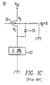
図1Cおよび図1Dにおいて、陽電位または供給Vccに接続されたパワーMOSFETは、接地または負電位に接続された負荷と直列に接続される。MOSFET「スイッチ」が正電源に接続されるので、たとえ電流源として用いられていても、本願明細書ではこれを位相上ハイサイドスイッチまたはHSSと呼ぶ。 In FIGS. 1C and 1D, the power MOSFET connected to the positive or supply V cc is connected in series with a load connected to ground or a negative potential. Since the MOSFET “switch” is connected to the positive power supply, even if it is used as a current source, it is referred to herein as a phase high side switch or HSS.
従来の分離されていないCMOSプロセスを用いて、図1Cの回路20は、負荷23、およびNMOS22を含むHSSを含む。このようなプロセスでは、MOSFET22のボディコンタクトは必然的に基板に短絡され、すなわち接地される。NMOSがオンであってVSがVccに近い電位まで増大すると、−VSBの大きな逆バイアス電位がダイオード25にわたって発生する。結果として生じるボディ効果は、NMOS22のしきい値を実質的に増大させ、NMOS22の薄いゲート酸化膜を損傷することなく低いオン抵抗を達
成するために適切なゲートドライブを与えることを困難にする。
Using a conventional non-isolated CMOS process, the
図1Dの回路30におけるNMOS32などの統合型ソース−ボディ短絡を備えた装置を用いると、負荷33における電流は、ボディ効果によるしきい値変動を中和する必要なしに容易に制御することができる。このような位相では、ドレイン−ボディダイオード35は、MOSFETのドレイン端子およびソース端子とアンチパラレルなままで(すなわち逆バイアスだが並列)、すべての正常運転条件下で逆バイアスのままである。ソース電位にかかわらずVSB=0なので、ボディ効果は明白ではなく、トランジスタの導電特性は電流によっては実質的に変化しない。ソース−ボディ短絡はまた、特にソース−ボディ短絡が単一の場所で一緒に短絡されるのではなく大面積装置にわたって均一に分散することができれば、スナップバック効果(下記に説明)の危険性を減らすことにより、アバランシェ耐性を向上させる。ソース−ボディ短絡の大面積NMOSへの統合は、離散的な電源装置においては一般的であるが、P−型ボディがP−型基板から統合された形で分離されることを必要とし、これは従来のCMOSが提供できないものである。このような分離を提供するプロセスは製造が複雑であり、しばしば高温製造ステップを必要とする。
Using a device with an integrated source-body short, such as
図1E、図1Fおよび図1Gにおいて、パワーMOSFETは、ソースまたはドレインのいずれもが正または負の電源レールに恒久的に接続されてない双方向スイッチとして使用される。MOSFET「スイッチ」がいかなる供給にも接続されず、その代り、いずれの方向でも電流を遮断するかまたは電流を伝導することができるので、本願明細書ではこれを位相上ACスイッチ、または「パストランジスタ」と呼ぶ。 In FIGS. 1E, 1F, and 1G, the power MOSFET is used as a bi-directional switch where neither the source nor the drain is permanently connected to the positive or negative power rail. A MOSFET “switch” is not connected to any supply, but instead can either cut off current or conduct current in either direction, so this is referred to herein as an AC switch or “pass transistor on phase”. "
従来のCMOS製造を用いると、図1Eのパストランジスタ40は、接地されたボディ接続を備えたNMOS41ならびに逆バイアスされたソース−ボディダイオード42およびドレイン−ボディダイオード43を含む。「ソース」および「ドレイン」という用語は、パストランジスタまたはACスイッチの応用例において多少とも任意である。なぜならば、VSでバイアスされた端子かVDでバイアスされた端子かのいずれが所定の例においてより正であるかを決定することは、多くの場合不可能だからである。ダイオード42および43にわたる電圧が大きいので、ボディ効果がNMOS41のしきい値、オン抵抗および飽和電流に著しい変化を引起しかねず、性能の低いACスイッチにしてしまう。
Using conventional CMOS fabrication, the
ソース−ボディ短絡を備えた少なくとも2つのNMOS装置を必要とするACスイッチを実現するための代替的手法が図1Fの回路45に示され、そこでは、ドレイン−ボディダイオード48および49が背中合わせに接続されるように、NMOSトランジスタ46および47が共通ソースVSと直列に接続されている。そのオフ状態では、ゲート端子はソース端子VSにバイアスされ、それによってチャネル導電を防ぐ。直列に接続されたスイッチにわたって与えられた極性にかかわらず2つのダイオードのうち1つが逆バイアスのままなので、アンチパラレルボディダイオードを通る導電もまた妨げられる。
An alternative approach for implementing an AC switch that requires at least two NMOS devices with source-body shorts is shown in
そのオン状態では、共通ゲートがソース端子上でバイアスされている場合は常に、両方のトランジスタがオンになっているので、ACスイッチ45はいずれの方向にも電流を伝導することができる。結果として生じるACスイッチは、双方向に遮断でき、双方向に導電できる。電圧VSがVD1とVD2との間の電位でフロートするという事実にもかかわらず、VSB=0なのでボディ効果は明白ではなく、すなわち各トランジスタは統合型ソース−ボディ短絡を有する。このような装置は、十分な分離を有するかまたはDMOS装置を統合することができるいかなるプロセスにも容易に統合され得る。このような装置は、分離なしでは、他の構成要素または回路にモノリシックに統合され得ない。装置は共通ソースではなく共通ドレインと接続され得るが、依然として分離されたソース−ボディを必要とすることに注意されるべきである。
In its on state, whenever the common gate is biased on the source terminal, both transistors are on so that the
ACスイッチ45の不利益は、2つの直列に接続されたトランジスタが付加的な抵抗を示すので、その特定のオン抵抗が高いこと、すなわちRDSAが大きいことである。スイッチがどのようにでも並列に接続されていたならば、同じ領域スイッチでもスイッチ45の背中合わせの手法における抵抗の4分の1を示したであろう。
The disadvantage of the
このような1つのスイッチが図1Gの回路50に示され、対称なNMOS装置51およびボディ−バイアス発生(BBG)回路52を組合せる。BBG回路52の目的は、NMOS51のボディを装置にわたって与えられる最大の負電位へとバイアスすること、ドレイン−ボディダイオード55またはソース−ボディダイオード56のいずれかを、VS端子またはVD端子のいずれがより正であるかに依存して、逆バイアスすることである。このようにすることで、ダイオード導電はまず生じず、トランジスタのゲートがボディ電位にバイアスされると、装置がオフとなって双方向に遮断する。反対に、装置が対称であるので、ゲートが「オン」にバイアスされる場合、装置は双方向に導電するであろう。名称「ドレイン」および「ソース」は任意であり、単に回路素子を特定するために用いられることに注意されたい。
One such switch is shown in
例として示されたBBG回路は、相互結合型NMOSトランジスタ53および54を利用してNMOS51上のボディ電位VBを決定しバイアスするが、そうしながら、それら自体が基板から分離されたソース−ボディ短絡を含んでいなければならない。したがってスイッチ50は、ACスイッチ45の好ましい実現例が行なうようにはDMOSトランジスタを利用しない一方、他の回路とともにICに統合されるために依然として分離を必要とする。
The BBG circuit shown as an example utilizes the
スナップバック破壊効果の抑制
従来のCMOSの別の制限は、NMOS装置に分離されたソース−ボディ短絡を統合する必要性に加えて、特にNMOSトランジスタにおいてMOSFET動作での望ましくないスナップバック破壊効果を防止できないことである。
Suppressing Snapback Breakdown Effects Another limitation of conventional CMOS is that it prevents the undesirable snapback breakdown effects in MOSFET operation, especially in NMOS transistors, in addition to the need to integrate isolated source-body shorts in NMOS devices It is impossible.
スナップバック破壊とは、ある範囲の動作条件について電流の増大がトランジスタの電圧保持性能の「低下」に対応するような、装置の負性抵抗に至る現象を指す。負性抵抗は、特にパワー電子回路において問題であり、過電流、発振および不安定性、電気雑音、局部加熱、熱暴走および装置破壊さえも引起す。 Snapback breakdown refers to a phenomenon in which an increase in current leads to a negative resistance of the device, corresponding to a “decrease” in the voltage holding performance of the transistor, over a range of operating conditions. Negative resistance is particularly a problem in power electronic circuits, causing overcurrent, oscillation and instability, electrical noise, local heating, thermal runaway and even device breakdown.
パワーエレクトロニクスでは、装置に課される最大電圧または電流を意図的に劣化させるか制限するにあたって、通常ではない設計およびプロセス方法を伴う特別な装置構造を用いることを含む、また他の回路および適用方法による、どうにかして負性抵抗を防ごうとする方法が要求される。装置が過熱している場合でなければ、負の電気抵抗は概して、寄生バイポーラ導電、衝撃イオン化に起因する導電率変調、または双方の何らかの組合わせのいずれかの結果である。 In power electronics, including the use of special device structures with unusual design and process methods in intentionally degrading or limiting the maximum voltage or current imposed on the device, and other circuits and application methods There is a need for a method that somehow tries to prevent negative resistance. Unless the device is overheated, negative electrical resistance is generally the result of either parasitic bipolar conduction, conductivity modulation due to impact ionization, or some combination of both.
たとえば図2Aでは、P型基板61、P+基板コンタクト62、N+ドレイン64、N−ドリフト領域65、MOS絶縁ゲート69、およびN+ソース63を含む、低濃度ドープしたドレインNMOS60が、そのオン状態で、そのドレインにいくらかの正の電圧〜Vccが与えられて、バイアスされている。概略的に装置に重ねられているのは、アバランシェ、衝撃イオン化、または接合リークのいずれかから発生するドレイン−基板ダイオード電流を表わすドレインダイオード59である。P型基板61に流れる多数キャリヤ基板電流または「ホール」は、直列接続されるRDB基板抵抗67およびRSB基板抵抗68によって概略的に表わされる、抵抗電圧降下を示す。基板抵抗に起因して、ソース63の下に位置するバルク基板における結果として生じる電圧VBは、P+コンタクト62に接続された接地端子より高圧に上昇する。この電圧が1ボルトの数十分の1に近づく場合、N+
領域63は、装置における二次元の電界によって、この場合N+ドレイン64である最も正の電位に当然に引寄せられる電子、すなわち少数キャリヤを基板61に注入し始めることができる。この電子導電機構は、N+コレクタ64、P型基板ベース61およびN+エミッタ63を含む、寄生NPNバイポーラトランジスタ66によって表わされる。バイポーラトランジスタの電圧維持性能が簡単なP−N接合ダイオードよりも(電流利得のために)低いので、NPN66の維持電圧はNMOS自体よりも低く、電圧はより低い値BVCERへとスナップバックする。この表記はバイポーラのコレクタ−エミッタ電圧を記述し、抵抗性で短絡されていないベースコンタクトを有する。
For example, in FIG. 2A, a lightly doped
図2Bの断面図に示されたスナップバックに至る別の機構が、MOSFETのドレインにおける衝撃イオン化である。この場合、NMOSは、高圧Vccにバイアスされ、それによって、N+ドレイン64およびP型基板61を含むドレイン−基板接合を逆バイアスする。電圧は、電圧0V(基板)、V1、V2、V3、V4およびV5における等電位曲線71によって示された空乏領域にわたって降下し、曲線ごとに電圧電位の大きさが増大している。このようなバイアス条件下のN−ドリフト領域は空乏化し、等電位線がN−ドリフト領域と基板との間の接合境界を横断することを可能にする。
Another mechanism leading to the snapback shown in the cross-sectional view of FIG. 2B is impact ionization at the drain of the MOSFET. In this case, the NMOS is biased to a high voltage V cc , thereby reverse biasing the drain-substrate junction including the N +
理想的には、これらの等電位線はドリフト領域に沿って直線的に間隔を置かれ、与えられた電圧の半分がゲート69とN+ドレイン64との間のドリフト領域の中央にあるべきである。しかしながら、表面電荷および他の避けられない表面効果のために、等電位線は均一には広がらず、その代り、ゲート縁部の近くで「束になり(bunch up)」結果としてドリフト領域の終わりにおいて局所的な高電界を生じる。さらに悪いことに、高電界は物理的に大電流密度領域の近くに位置する。装置が電流を伝導しながら高ドレイン電位を有する飽和では、矢印72によって表示される主電流路はゲートの下を流れ、次いで、空乏化したドリフト領域65の縁部に接近するつれて表面から離れて流れる。大電流密度および高電界の生成物は、結晶の原子構造と高速電子との衝突に起因して、衝撃イオン化すなわち局所的なキャリヤ生成を結果として生じる。この衝突によって価電子は原子を接合することから外され、価電子はさらに自由な導電電子に変換されて、次に局所的に高い電界によっても加速される。
Ideally, these equipotential lines should be linearly spaced along the drift region and half of the applied voltage should be in the center of the drift region between the gate 69 and the N + drain 64. . However, due to surface charge and other unavoidable surface effects, the equipotential lines do not spread uniformly and instead end up at the end of the drift region as a result of “bunching up” near the gate edge. Produces a high local electric field. Even worse, the high electric field is physically located near the high current density region. In saturation where the device conducts current and has a high drain potential, the main current path, indicated by
結果として生じる衝撃イオン化は、本願明細書では、発生の増大を表わす同心の輪郭73によって表わされる。衝撃イオン化が電子−ホールの対を生成するので、2つの望ましくない効果を結果として生じる。第1に、電子が結晶に相対して高エネルギに加速され、すなわちエネルギ的に「熱く」なり、ゲート酸化膜に向かって流されて誘電体を破損しかねない。第2の現象は、生成されたホール電流が基板抵抗RSBにわたってさらなる電圧降下の一因となってNPNスナップバック効果を悪化させることである。
The resulting impact ionization is represented herein by a
さらに高速の衝撃イオン化および大電流では、別の現象が生じる。このような場合、生成されたキャリヤは、局所的な空間電荷中立(space charge neutrality)を変更するのに十分な追加の電荷の導入によりドリフト領域の局所的な導電率を変更し始める。追加の電子は追加のホールを引寄せ、それはドリフトドーピングの増大のように作用する。より高濃度の有効なドープはN層に広がる空乏を減少させ、等電位がさらに束になるよう強制し、ドリフト領域の縁部で局所的な電界を実質的に増大させ、さらに衝撃イオン化を増大させる。その結果、より多くの衝撃イオン化が高い局所電場を引起こし、さらにより大きな電流の一因となるので、負性抵抗の別の原因となる。さらに、2つの負性抵抗効果が同時に生じる場合があり、複雑で予測不能な態様で相互作用する。この機構にかかわらず、NMOSが所与の電流で維持することができるドレイン電圧が結果として低下する。 Further phenomena occur at higher impact ionization and higher currents. In such a case, the generated carriers begin to change the local conductivity of the drift region by the introduction of additional charge sufficient to change the local space charge neutrality. Additional electrons attract additional holes, which act like increased drift doping. Higher effective doping reduces depletion spreading to the N layer, forces the equipotentials to become more bundled, substantially increases the local electric field at the edge of the drift region, and further increases impact ionization Let As a result, more impact ionization causes a higher local electric field and contributes to even higher currents, which is another source of negative resistance. In addition, two negative resistance effects may occur simultaneously and interact in a complex and unpredictable manner. Regardless of this mechanism, the drain voltage that the NMOS can sustain at a given current results in a decrease.
電気的に、スナップバックの現象は、図2Cのドレイン電流ID対ドレイン電圧VDのグラフ75に示される。曲線76によって示される理想的な装置破壊BVDSSは、曲線7
7によって示されるスナップバック電圧BVCERよりも電圧において2倍以上も実質的に大きいことがある。ドレインが電圧BVDSSを維持しつつ大電流でアバランシェに駆動されると、突然BVCERに落下して電流の増大を引起し、装置を破壊し得る。NMOSが電流源として作動し、またはオンからオフへ切替えている場合、スナップバックの開始は、衝撃イオン化により増大した基板リークによって悪化し得る。曲線78、69、80および81は、装置がBVCERより上のいかなる電圧で作動するにも有用ではないことを示す。
Phenomenon of electrical snapback is shown in the
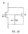
The voltage may be substantially more than twice as large as the snapback voltage BV CER indicated by 7. If the drain is driven to an avalanche with a large current while maintaining the voltage BV DSS, it can suddenly drop into the BV CER causing an increase in current and destroying the device. When the NMOS is operating as a current source or switching from on to off, snapback initiation can be exacerbated by increased substrate leakage due to impact ionization.
スナップバックの開始の1つの理由は、特に基板が低濃度ドープされる場合、N+ソース63とボディコンタクト62と間の、およびその下のRSB基板抵抗68が大きすぎることである。他の効果は、低濃度ドープした基板には十分なベース電荷がないので、寄生NPN利得が大きすぎることである。NPNトランジスタの悪影響を減じる明らかな1つの方法は、基板ドープを増大させることであるが、不運にもそうすることによってドレインで電界を増大させることにもなり、さらにより多くの衝撃イオン化および基板電流を生じる。
One reason for initiating snapback is that the RSB
スナップバック効果は、MOSFETに関連付けられた寄生バイポーラを示すことによりしばしば概略的に表わされる。たとえば、図2Dの回路85は、寄生NPN87を備えたNMOS86、および抵抗器88を短絡するベースへの非線形のエミッタを示す。同様に、PMOSは寄生PNPを含むが、PNP利得がNPN利得よりもはるかに低いので、かつホットホールに引起された衝撃イオン化率が電子イオン化率よりもはるかに低いので、スナップバック現象はPMOSにおいてはNMOSにおいてほどは問題にならない。
The snapback effect is often represented schematically by showing the parasitic bipolar associated with the MOSFET. For example,
従来のDMOS製造
付加的なチャネルドーピングを通してスナップバックを抑え、ドレイン電界を増大させずに基板抵抗を下げる1つの方法は、DMOS電界効果トランジスタを形成することによる。文字「D」が二重(元来は二重拡散)を表わす名称のDMOSは、ゲートの下のチャネルまたはボディのドーピングは均一ではないが、ドレイン領域の近くの電界を悪い方向に増大させる)ことを回避するためにゲートのソース側の近くで濃縮されているか局所化されているところに構築される。このように、チャネル濃度は衝撃イオン化またはドレイン電圧破壊電圧に影響を与えずに調整することができる。
Conventional DMOS Fabrication One way to suppress snapback through additional channel doping and reduce substrate resistance without increasing the drain field is by forming a DMOS field effect transistor. (The DMOS whose name “D” represents double (originally double diffusion), the channel or body doping under the gate is not uniform, but the electric field near the drain region is adversely increased) To avoid that, it is built where it is concentrated or localized near the source side of the gate. Thus, the channel concentration can be adjusted without affecting impact ionization or drain voltage breakdown voltage.
DMOS電界効果トランジスタは分離されたバージョンでも分離されないバージョンでもよい。従来の技術では、分離されたものは、一般にP型基板の上に成長されるN型エピタキシのエピタキシャル堆積の使用を必要とする。 The DMOS field effect transistor may be an isolated version or a non-isolated version. In the prior art, isolation requires the use of epitaxial deposition of N-type epitaxy that is typically grown on a P-type substrate.
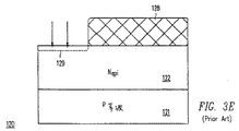
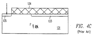
図3Aに示されるように、N型エピタキシャル層92はP型基板91の上に成長して、分離されたDMOS装置90を形成し、ゲートポリシリコン98、ゲート酸化膜99、N+ドレインコンタクト94、N+ソース96、P+ボディコンタクト97およびP型「ボディ」またはDMOSトランジスタに特有のPB領域93をさらに含む。N−ドリフト領域95は任意であり、低いオン抵抗を達成するのにエピタキシャルドーピングが十分な場合には必要ではないかもしれない。破壊と抵抗との間のトレードオフを最適化するために追加のN−ドリフトドーピングが付加されてもよいが、ゲートがドリフト領域を並置する場合は衝撃イオン化効果によって制限されたままである。
As shown in FIG. 3A, an N-
代替的形状ではN型エピタキシャル層はP型エピタキシャル層または基板と置換することができるが、するとN−ドリフト領域95が装置動作のために必須となる。しかしながら、N型エピタキシャル層なしではDMOSは分離されず、そのP型ボディは電気的に接地すなわち基板に短絡される。
In an alternative configuration, the N-type epitaxial layer can be replaced with a P-type epitaxial layer or substrate, but an N-
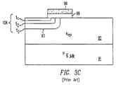
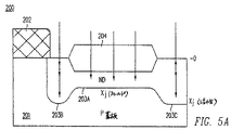
従来のDMOS製造が図3Bの断面100および図3Cの断面105に示される。示されるように、エピタキシャル層92はパターニングされたフォトレジスト101によって覆われ、低エネルギでホウ素注入されて浅い層102を形成する。この注入は、典型的には50から100keVの低エネルギで、たとえばウェーハの表面に3度だけ軸外しでほぼ直交してゲート98の下に限定的に横向きに浸透するよう実行される。
Conventional DMOS fabrication is shown in
次いでこの注入層が駆動され、すなわち長時間高温で拡散されて、図3Cに示されるように、接合93を形成するようゲート98の下でドーパントを横方向に拡張する。7〜24時間のいずれかの時間行なわれる拡散は、1050°Cを超える、典型的には1100°C以上の高温を必要とし、これは多くの近代的な低温製造施設および大きなウェーハ直径とは相容れないプロセスである。図3Cに示され、かつ時間t1、t2、およびt3における拡散106によって示されるような拡散の進行は横方向にも垂直方向にも生じ、そこでは横方向の拡張は垂直の接合深さのおよそ80%である。示されたバージョンでは、ボディ拡散層は、ゲートが形成された後に注入されたので、ゲートに自己整合する。
This implant layer is then driven, i.e., diffused at an elevated temperature for an extended period of time, extending the dopant laterally under the
低温プロセスが必要な場合、DMOS装置を形成する別の自己整合した製造方法が図3Dに示される。この手法では、ボディ注入は典型的には数十万電子ボルトのより高エネルギで実行されるが、より重要なことには、急な角度、たとえば45°で行なわれて、ボディドーパントが完全にN+ソース96を囲むのに十分な程度にゲート98の下で横方向に浸透することを保証する。横方向の注入方法は、ウェーハ上の4つのゲート配向をすべて覆うために注入を4時間実行しなければならないので、製造用としては複雑で望ましくない。注入中にウェーハを回転させることは均一な注入を困難にする。
If a low temperature process is required, another self-aligned manufacturing method for forming a DMOS device is shown in FIG. 3D. In this approach, body implantation is typically performed at a higher energy of hundreds of thousands of electron volts, but more importantly, it is performed at a steep angle, for example 45 °, so that the body dopant is completely Ensure lateral penetration under the
別のDMOS製造方法は、図3Eから図3Gまでに示されるように自己整合されないDMOS120を形成することである。図3Eでは、浅いホウ素注入層129が、パターニングされたフォトレジスト128によってマスキングされたエピタキシャル層122に形成される。次いで注入層は、長期間の間、図3Fに示されるように高温で拡散される。P型領域は、増加する時間t1、t2、t3、およびt4においてP−N接合を表わす曲線123によって示されるように、垂直にも横方向にも拡散する。最後に、図3Gでは、下層のゲート酸化膜126を備えたゲート電極125が、表面での接合がゲート縁部127Aおよび127B間に位置するように、接合124の縁部の上に位置決めされる。ゲート125および接合124の相対的位置は自己整合されないので、製造中にマスク不整合にさらされる。
Another DMOS fabrication method is to form a
記載されたすべての場合において、高温拡散のプロセスによって、DMOSボディ領域のドーパント濃度プロファイルがモノリシックに減少するに至り、ウェーハの表面で最も濃度が高い。不運にも、このようなプロファイルは、表面から遠ざかったバルクで表面電界がより高いことを意味し、強固なアバランシェ耐性のある装置の製造用としては理想的ではない。 In all cases described, the high temperature diffusion process leads to a monolithic reduction in the dopant concentration profile of the DMOS body region, with the highest concentration at the surface of the wafer. Unfortunately, such a profile means that the surface electric field is higher in the bulk away from the surface and is not ideal for the production of a robust avalanche resistant device.
DMOSボディ製造に含まれる高温拡散は、従来のエピタキシャル接合分離を用いた回路の十分な電気分離性を達成するために必要とされるステップによってさらに複雑になる。 The high temperature diffusion involved in DMOS body fabrication is further complicated by the steps required to achieve sufficient electrical isolation of circuits using conventional epitaxial junction isolation.
図4Aから図4Iまでに示されたような従来の先行技術プロセスでは、p型基板131はフォトレジスト132によってマスキングされ、ヒ素またはアンチモン133によって注入され、次にフォトレジスト134によって再びマスキングされて、図4Cに示されるようにホウ素135が注入される。次いで注入層はしばしば1200℃にまでなる非常な高温で24時間もの間拡散され、エピタキシャル成長よりも前に、動きの遅いアンチモンを、基板に対し、かつ表面から離れるように拡散させる。そのような拡散の間に、埋込層
のガス放出からの横方向のドーピングから表面を保護するために、酸化膜138が成長する。アンチモンNBL層136Aの上の酸化膜の成長率がホウ素PBL層137Aの上おけるよりも速いので、この酸化もまたその後のマスク整合のためのウェーハにおけるパターンの規定を助けるために用いられる。
In a conventional prior art process as shown in FIGS. 4A-4I, a p-
埋込層拡散後に、図4Eに示されるように、酸化膜は剥がされて、エピタキシャル成長の最初にその場でHCI酸性エッチングが実行され、それによって頂部のシリコン層を取除き、接着を向上させ、かつエピタキシャル層の結晶欠陥を減じる。エピタキシャル成長の結果は図4Fに示され、そこではエピタキシャル層がすでに拡張しているNBL領域136BおよびPBL137Bをカバーし、その両方が高温成長中にエピタキシャル層の中へと上方拡散する。 After buried layer diffusion, as shown in FIG. 4E, the oxide is stripped and an HCI acidic etch is performed in situ at the beginning of epitaxial growth, thereby removing the top silicon layer and improving adhesion, In addition, crystal defects in the epitaxial layer are reduced. The result of the epitaxial growth is shown in FIG. 4F, where the epitaxial layer covers the already expanded NBL regions 136B and PBL 137B, both of which diffuse upward into the epitaxial layer during high temperature growth.
次に、図4Gおよび図4Hに示されるように、高用量リン注入層140がマスク141を通して導入され、次にフォトレジストマスク143を通して高用量ホウ素注入142が続く。長い高温分離拡散の後、P型分離領域145は、P型埋込層PBL137Cの部分に接続する。同様に、N型シンカ拡散144は埋込層NBL 136Cに接続する。拡散の深さおよび必要となる時間は、エピタキシャル層139の厚さおよびプロセスでの他の続く高温拡散に依存する。高温拡散はまた、埋込層がさらに横方向に拡張して、前の処理ステップでのサイズすなわち137Bおよび136Bよりも大きな137Cおよび136Cを形成するために上方拡散する。
Next, as shown in FIGS. 4G and 4H, a high dose
いかなるDMOSボディ拡散も、すべての接合深さおよび埋込層の上の正味のエピタキシャル厚さをも変更し、これらすべてによって製造処理が複雑かつ特定のエピタキシャル厚さに特有のものとなる。epi厚さが装置の電圧定格を決定するので、プロセス全体および対応する設計ルールはすべて電圧に特有である。 Any DMOS body diffusion changes all junction depths and the net epitaxial thickness above the buried layer, all of which make the manufacturing process complex and specific to a particular epitaxial thickness. Since the epi thickness determines the voltage rating of the device, the entire process and the corresponding design rules are all voltage specific.
高圧装置に対する低温モジュール製造の適応
以前に記載されたように、高圧装置を製造し、分離し、かつ統合するために用いられる従来のエピタキシャルプロセスおよび高温プロセスならびに生産方法の問題点は、各高温プロセスがすべての高圧装置および低圧装置に影響するドーパント再分布を引起こすことである。さらに高温製造によって、大きな直径のウェーハおよび近代的なサブミクロンウェーハ製造工場、すなわち高密度トランジスタ統合、大規模ダイ、および低製造コストでの高い歩留まりを可能にする製造工場の使用が妨げられる。
Adaptation of low temperature module manufacturing to high pressure equipment As previously described, the problems with conventional epitaxial and high temperature processes and production methods used to manufacture, isolate and integrate high pressure equipment are Cause dopant redistribution that affects all high and low pressure devices. In addition, high temperature manufacturing prevents the use of large diameter wafers and modern submicron wafer manufacturing plants, that is, high density transistor integration, large dies, and manufacturing plants that enable high yields at low manufacturing costs.
必要なものは、高温処理およびエピタキシの必要性をなくすような、低圧CMOSの完全に分離されたフローティングポケット、バイポーラトランジスタ、ダイオードおよび受動回路構成要素と、高圧トランジスタおよびDMOSトランジスタとが統合されるプロセスである。理想的には、このような製造プロセスは、最終ドーパントプロファイルが、いかなるその後のウェーハ処理ステップによってもその本来の注入されたプロファイルから実質的に不変のままであるような、「注入されたままの(as-implanted)」ドーパントプロファイルを使用するべきである。理想的には、このプロセスは、プロセスの装置製造所において利用可能な他の装置を変えることなく、装置が加えられたり省略されたり、統合された流れに対応するプロセスステップが加えられたり取除かれたりするような、モジュール式のアーキテクチャに構築されるべきである。 What is needed is a process where low voltage CMOS fully isolated floating pockets, bipolar transistors, diodes and passive circuit components are integrated with high voltage transistors and DMOS transistors, eliminating the need for high temperature processing and epitaxy. It is. Ideally, such a manufacturing process is “as implanted” such that the final dopant profile remains substantially unchanged from its original implanted profile by any subsequent wafer processing steps. An “as-implanted” dopant profile should be used. Ideally, this process would add or omit equipment or add or remove process steps corresponding to an integrated flow without changing the other equipment available in the equipment fab of the process. It should be built into a modular architecture.
発明の要約
この発明に従って、一連のプロセスが用いられ、高圧トランジスタおよびDMOSトランジスタが、低圧CMOSの完全に分離されたフローティングポケット、バイポーラトラ
ンジスタ、ダイオードおよび受動回路構成要素と統合される。このプロセスは、高温処理およびエピタキシの必要をなくし、最終ドーパントプロファイルが、いかなるその後のウェーハ処理ステップによってもその本来の注入されたプロファイルから実質的に不変のままであるような、「注入されたままの」ドーパントプロファイルを使用する。それとともに、このプロセスは、IC上の他の装置を生産するために用いられるプロセスを変える必要なく、装置がICに加えられたり省略されたりすることや、対応するプロセスステップが統合された流れに加えられたり取除かれたりすることを可能にする、モジュール式のアーキテクチャを形成する。
SUMMARY OF THE INVENTION In accordance with the present invention, a series of processes are used to integrate high voltage and DMOS transistors with low voltage CMOS fully isolated floating pockets, bipolar transistors, diodes and passive circuit components. This process eliminates the need for high temperature processing and epitaxy, and remains “implanted” such that the final dopant profile remains substantially unchanged from its original implanted profile by any subsequent wafer processing steps. The “dopant” profile is used. At the same time, this process does not require changing the process used to produce other devices on the IC, so that devices can be added to or omitted from the IC and the corresponding process steps can be integrated. Forms a modular architecture that can be added and removed.
有利には、このプロセスはエピタキシャル層のない基板上で実行され、エピタキシャル層の形成を含まない。 Advantageously, this process is performed on a substrate without an epitaxial layer and does not involve the formation of an epitaxial layer.
これらの低温プロセスを使用すると、いくつかの独特の高圧装置および電源装置が製造されてモジュール方式でICに統合され得る。ここに含まれるのは、分離されないラテラルDMOS、分離されない拡張されたドレインMOS装置またはドリフトされたMOS装置、ラテラルトレンチDMOS、分離されたラテラルDMOS、JFETおよび空乏モード装置、ならびにP−Nダイオードクランプおよびレクチファイヤおよび基板に対して高圧にフロートする低圧構成要素のための接合終端部である。 Using these low temperature processes, several unique high voltage devices and power supplies can be manufactured and modularly integrated into the IC. Included herein are non-isolated lateral DMOS, non-isolated extended drain or drifted MOS devices, lateral trench DMOS, isolated lateral DMOS, JFET and depletion mode devices, and PN diode clamps and A junction termination for a low pressure component that floats to a high pressure relative to the rectifier and substrate.
分離されないDMOSを製造するプロセスは、フィールド酸化膜層を通したコンフォーマルドリフト領域の注入と、フィールド酸化膜層の第1の端部におけるドリフト領域内のそのドレイン領域の注入と、フィールド酸化膜層の第2の端部のゲート形成と、フィールド酸化膜層の第2の端部近くのボディ領域の注入と、ボディ領域内のソース領域の注入とを含む。ドリフト領域およびボディ領域は、非ガウスの垂直ドーパントプロファイルを生成するために、連鎖状の注入層によって形成されてもよい。分離されないDMOSは、ドレイン中心の形状で製造されてもよい。1つの実施例では、フィールド酸化膜層は省略されてもよく、非ガウスの垂直ドーパントプロファイルを生成するために、ドリフト領域およびボディ領域は連鎖状の注入層で製造されてもよい。別の一連の実施例では、ラテラルDMOSは、より強固なアバランシェ耐性のある装置を生成するために、ツェナダイオードクランプを用いて形成されてもよい。装置は拡張されたドレインを伴って形成されてもよく、ゲートはドレインを囲んでも囲まなくてもよい。 The process of manufacturing a non-isolated DMOS includes the implantation of a conformal drift region through the field oxide layer, the implantation of its drain region in the drift region at the first end of the field oxide layer, and the field oxide layer. Forming a gate at the second end, implanting a body region near the second end of the field oxide layer, and implanting a source region in the body region. The drift region and body region may be formed by a chained implant layer to produce a non-Gaussian vertical dopant profile. A non-isolated DMOS may be manufactured with a drain centered shape. In one embodiment, the field oxide layer may be omitted and the drift and body regions may be fabricated with a chained implant layer to produce a non-Gaussian vertical dopant profile. In another series of embodiments, the lateral DMOS may be formed using a Zener diode clamp to produce a more robust avalanche resistant device. The device may be formed with an extended drain and the gate may or may not surround the drain.
分離されていない拡張されたドレインまたはドリフトされたMOS装置を製造するプロセスは、ドレインを囲むことができるゲートに対して自己整合された拡張されたドレインを備えたドレイン中心の装置を生成することができる。この装置は非ガウスウェルに形成されてもよい。代替的実施例では、装置は非対称であってゲートはドレインを囲まない。この非対称の構造を用いてCMOSの対が製造されてもよい。 The process of manufacturing an unisolated extended drain or drifted MOS device can produce a drain-centric device with an extended drain that is self-aligned to a gate that can surround the drain. it can. The device may be formed in a non-Gaussian well. In an alternative embodiment, the device is asymmetric and the gate does not surround the drain. CMOS pairs may be fabricated using this asymmetric structure.
ラテラルトレンチDMOS(LTDMOS)を製造するプロセスは、トレンチゲートの形成、トレンチの底部近くのレベルまで延在し得るドリフト層の形成、好ましくは注入エネルギおよび用量が変動する連鎖注入層を用いることによる注入されたままのボディの形成、ならびにソース領域およびドレイン領域の形成を含み得る。この装置は、トレンチゲート中心の形状で製造され得る。LTDMOSは、コンフォーマルドリフト領域に囲まれ得る深いドレイン領域を含んでいてもよい。装置はドレイン中心の形状に製造されてもよい。装置は、半導体材料の表面にフィールド酸化膜セグメントを適切に配置することによって、トレンチおよびドレインの近くにより深い部分を有するコンフォーマルドリフト領域を含んでいてもよい。 The process of manufacturing a lateral trench DMOS (LTDMOS) is the formation of a trench gate, the formation of a drift layer that can extend to a level near the bottom of the trench, preferably by using a chain implant layer with variable implant energy and dose. Formation of the as-made body, and formation of the source and drain regions. This device can be manufactured in the shape of a trench gate center. The LTDMOS may include a deep drain region that may be surrounded by a conformal drift region. The device may be manufactured in the shape of the drain center. The device may include a conformal drift region having deeper portions near the trench and drain by appropriately placing field oxide segments on the surface of the semiconductor material.
分離されたラテラルDMOSを製造するプロセスは、典型的には基板と反対の導電性を有する深い層を注入することを含む。フィールド酸化膜層の開口部を通して深い層を注入
することによって、深い層は受け皿の形になることができ、分離されたポケットを形成するように、縁部がフィールド酸化膜層の縁部まで上向きに延在する。ボディ領域は、連鎖注入層を用いて分離されたポケット内に注入されてもよい。ドリフト領域もまたポケットに注入されてもよい。代替的には、フィールド酸化膜層は省略されてもよく、その場合には、深い層は実質的に平らである。分離されたポケットは、半導体表面から下向きに延在して深い層と重なる、注入されたウェルを用いて形成されてもよい。ラテラルDMOSはボディ領域に対して対称であり得る。
The process of manufacturing an isolated lateral DMOS typically involves injecting a deep layer having a conductivity opposite that of the substrate. By injecting a deep layer through the opening in the field oxide layer, the deep layer can be shaped as a saucer, with the edges facing up to the edge of the field oxide layer to form separate pockets. Extend to. The body region may be implanted into the pockets separated using a chain implantation layer. A drift region may also be implanted in the pocket. Alternatively, the field oxide layer may be omitted, in which case the deep layer is substantially flat. The isolated pockets may be formed using implanted wells that extend downward from the semiconductor surface and overlap a deep layer. The lateral DMOS can be symmetric with respect to the body region.
接合電界効果トランジスタ(JFET)を製造するプロセスは、基板と反対の導電型を有するドリフト領域の注入、ならびにドリフト領域内のソース、ドレインおよびボディ(ゲート)領域の注入を含んでいてもよい。ソース領域およびドレイン領域はドリフト領域と同じ導電型であり、ボディ(ゲート)は基板と同じ導電型である。ドレイン領域は深い連鎖注入層を含んでもよい。 The process of manufacturing a junction field effect transistor (JFET) may include implanting a drift region having a conductivity type opposite to the substrate, and implanting source, drain and body (gate) regions within the drift region. The source region and the drain region have the same conductivity type as the drift region, and the body (gate) has the same conductivity type as the substrate. The drain region may include a deep chain injection layer.
空乏モードMOS装置を製造するプロセスは、半導体表面の上にゲートを形成することと、ゲートに自己整合されたドリフト領域を注入することと、ソース領域およびドレイン領域を注入することとを含み得る。そのプロセスはまた、深いドレイン領域を形成するように連鎖注入層を用いることを含んでもよい。代替実施例では、ドリフト領域はゲートの形成に先立って注入され、したがって、ゲートに自己整合されない。さらに別の実施例では、深いコンフォーマルドリフト領域がゲートの形成に先立って注入される。先の実施例の各々は、NPN寄生バイポーラ導電の開始を減じ、かつスナップバック効果を抑えるために、表面下シールドを含むよう修正されてもよい。空乏モード装置はまた、深いドレインとしても機能し得る環状のサイドウォール分離ウェルが深い分離層に重ねられた、完全に分離された形で製造されてもよい。 A process for manufacturing a depletion mode MOS device may include forming a gate over a semiconductor surface, implanting a drift region that is self-aligned to the gate, and implanting a source region and a drain region. The process may also include using a chain injection layer to form a deep drain region. In an alternative embodiment, the drift region is implanted prior to gate formation and is therefore not self-aligned to the gate. In yet another embodiment, a deep conformal drift region is implanted prior to gate formation. Each of the previous embodiments may be modified to include a subsurface shield to reduce the onset of NPN parasitic bipolar conduction and suppress the snapback effect. The depletion mode device may also be fabricated in a fully isolated form, with an annular sidewall isolation well that can also function as a deep drain, superimposed on a deep isolation layer.
ダイオードを製造するプロセスは、アノードまたはカソードを形成するために複数の注入層または連鎖注入層を用いることを含んでもよく、それによって、より深い部分が表面部分よりも高濃度になる領域を形成する。分離されたダイオードは、深い層と、深い層に隣接してアノード領域およびカソード領域を囲む環状ウェルとを注入することにより、形成され得る。 The process of manufacturing the diode may include using multiple injection layers or chain injection layers to form the anode or cathode, thereby forming a region where the deeper portion is more concentrated than the surface portion. . An isolated diode can be formed by implanting a deep layer and an annular well surrounding the anode and cathode regions adjacent to the deep layer.
この発明のプロセスはまた、分離されたP−型ポケットを基板の上の高圧にフロートさせるための終端縁部を形成するために用いられてもよい。プロセスの変形例は、レベル間誘電体またはフィールド酸化膜層の上における金属またはポリシリコンのフィールドプレートの形成を含む。分離構造のサイドウォールを形成するN−ウェルは、フィールド酸化膜層の下で横方向に延在することができる。別の実施例は、N−ウェルの縁部と重なり、フィールド酸化膜層の上に延在する部分を有するポリシリコンフィールドプレートを含む。別の実施例では、終端は、N−ウェルに接続された、レベル間誘電体またはフィールド酸化膜層の下に延在する深いN−ドリフト領域を含む。いくつかの実施例では、分離構造の床を形成する深いN層は、分離されたポケットを越えて横方向に延在する。 The process of the present invention may also be used to form a termination edge for floating the isolated P-type pocket to a high pressure over the substrate. Process variations include the formation of metal or polysilicon field plates over interlevel dielectric or field oxide layers. The N-well that forms the sidewalls of the isolation structure can extend laterally under the field oxide layer. Another embodiment includes a polysilicon field plate having a portion that overlaps the edge of the N-well and extends over the field oxide layer. In another embodiment, the termination includes a deep N-drift region extending below the interlevel dielectric or field oxide layer connected to the N-well. In some embodiments, the deep N layer that forms the floor of the isolation structure extends laterally beyond the isolation pocket.
発明の詳細な説明
米国特許第6,855,985号は、注入されたままの接合分離構造を用いる全低温製造方法を記載する。この方法は、分離拡散、エピタキシまたは高温プロセスの必要なしに、完全に分離されたバイポーラ、CMOSおよびDMOS装置を達成するために、湾曲した酸化膜を通して注入されたドーパントを備えた高エネルギかつ連鎖注入を利用する。
DETAILED DESCRIPTION OF THE INVENTION US Pat. No. 6,855,985 describes an all-low temperature manufacturing method using an as-injected junction isolation structure. This method is a high energy and chain implant with dopant implanted through a curved oxide to achieve fully isolated bipolar, CMOS and DMOS devices without the need for isolation diffusion, epitaxy or high temperature processes. Is used.
この出願の主題は上記に言及された特許に関連し、さまざまな種類の新規な、または向上した高圧装置およびDMOS装置、スナップバック予防、分離されたクランピングダイオードおよびレクチファイヤの設計および統合、ならびに分離されたポケットにおける低電圧装置を基板電位を超える高圧にフロートさせる方法に焦点を合わせる。 The subject matter of this application relates to the patents referred to above, and includes various types of new or improved high voltage and DMOS devices, snapback prevention, isolated clamping diode and rectifier design and integration, and The focus is on how to float the low voltage device in the isolated pocket to a high voltage above the substrate potential.
本願明細書に記載された高圧装置の低温製造は前述の特許および特許出願に記載されたモジュール式低温製造方法と互換性を有するが、モジュール式プロセスアーキテクチャに必ずしも限定されるわけではない。 The low temperature manufacturing of the high pressure apparatus described herein is compatible with the modular low temperature manufacturing methods described in the aforementioned patents and patent applications, but is not necessarily limited to a modular process architecture.
ウェーハ製造
特に明記しない限り、本願明細書に記載された高圧および高電力装置の製造は上記で参照された特許と同じプロセスシーケンスを利用する。基本的なプロセスの概略は以下を含む。
・ フィールド酸化膜の形成
・ 平坦化を含むトレンチおよびトレンチゲートの形成
・ 高エネルギ注入された深いドリフト層(ND)の形成
・ 連鎖注入トレンチDMOSボディ(P−ボディ)の形成
・ リン高エネルギ注入された床分離(DN)の形成
・ 第1の連鎖注入された非ガウスのN−ウェル(NW1/NW1B)の形成
・ 第1の連鎖注入された非ガウスのP−ウェル(PW1/PW1B)の形成
・ 第2の連鎖注入された非ガウスのN−ウェル(NW2/NW2B)の形成
・ 第2の連鎖注入された非ガウスのP−ウェル(PW2/PW2B)の形成
・ 2重ゲート酸化膜およびゲート電極の形成
・ N−ベース注入
・ P−ベース注入
・ 第1のN−LDD注入(NLDD1)
・ 第1のP−LDD注入(PLDD1)
・ 第2のN−LDD注入(NLDD2)
・ 第2のP−LDD注入(PLDD2)
・ サイドウォールスペーサの形成
・ ESD注入
・ N+注入
・ P+注入
・ 高速熱アニール(RTA注入活性化)
・ 多層金属相互接続プロセス
・ 不動態化
記載されたプロセスがドーパント再分布が僅かしかないかまたは全くない注入されたままのドーパントプロファイルを利用するので、P−ウェルおよびN−ウェル注入がゲート形成に先行し、トレンチゲート形成がDMOSボディ注入に先行し、N−LDDおよびP−LDD注入はゲート形成に続くがサイドウォールスペーサ形成に先行し、N+およびP+注入がサイドウォールスペーサ形成に続くことが好ましいことを除いて、注入は実際にはいかなる順に実行されてもよい。このプロセスフローは、モジュール式であるよう設計されているので、そのIC設計にいずれの組の装置が必要かに依存して、所与のICの製造のための1つ以上のプロセスステップをなくすことが可能である。
Wafer Manufacture Unless otherwise specified, the fabrication of high voltage and high power devices described herein utilizes the same process sequence as the above referenced patents. The basic process outline includes:
・ Formation of field oxide film ・ Formation of trench and trench gate including planarization ・ Formation of deep drift layer (ND) with high energy implantation ・ Formation of chain implantation trench DMOS body (P-body) ・ High energy implantation with phosphorus Formation of a closed bed separation (DN) Formation of a first chain-injected non-Gaussian N-well (NW1 / NW1B) Formation of a first chain-injected non-Gaussian P-well (PW1 / PW1B) Formation of second chain-implanted non-Gaussian N-well (NW2 / NW2B) Formation of second chain-implanted non-Gaussian P-well (PW2 / PW2B) Double gate oxide and gate Electrode formation, N-base implantation, P-base implantation, first N-LDD implantation (NLDD1)
First P-LDD injection (PLDD1)
Second N-LDD injection (NLDD2)
Second P-LDD injection (PLDD2)
・ Sidewall spacer formation ・ ESD implantation ・ N + implantation ・ P + implantation ・ Rapid thermal annealing (RTA implantation activation)
• Multi-layer metal interconnect process • Passivation P-well and N-well implants for gate formation because the described process utilizes as-implanted dopant profiles with little or no dopant redistribution Preferably, trench gate formation precedes DMOS body implantation, N-LDD and P-LDD implantation follows gate formation but precedes sidewall spacer formation, and N + and P + implantation preferably follow sidewall spacer formation. Except that, the injection may actually be performed in any order. Because this process flow is designed to be modular, it eliminates one or more process steps for manufacturing a given IC, depending on which set of equipment is required for that IC design. It is possible.
例として、表1は、この出願に記載された注入のための好ましい実施例および好ましい条件範囲を要約する。 As an example, Table 1 summarizes the preferred examples and preferred condition ranges for the injections described in this application.

上記の注入のいくつかは、注入用量の合計が両面空乏拡散を支持するのに、またある場合にはアバランシェ降伏の開始に先立って層の完全な空乏を可能にするのに十分に低いので、高圧装置のドリフト領域を形成するのに潜在的に使用可能である。限定された注入用量(または電荷)の領域を十分に空乏化することによって装置における表面電界が高圧で
減じられる現象はまた、「RESURF」、すなわち減じられた表面フィールド(reduced surface fields)の頭文字で呼ばれる。歴史的には、RESURFという用語は限定された電荷のエピタキシャル層に用いられる一方、LDD、ドリフト領域またはドレイン拡張部は注入された層を指す。浅いLDD領域が典型的にMOSゲートに自己整合される一方で(ND注入層などの)高エネルギ注入された深いドリフト領域は典型的にはゲート形成に先行することを除いては、浅いLDDの利点対深いドリフト領域の利点は本願明細書では区別されない。
Some of the above injections are low enough to support double side depletion diffusion, and in some cases to allow full depletion of the layer prior to the onset of avalanche breakdown, It can potentially be used to form the drift region of a high pressure device. The phenomenon that the surface electric field in the device is reduced at high pressure by sufficiently depleting the limited injected dose (or charge) area is also referred to as “RESURF”, an acronym for reduced surface fields. Called by. Historically, the term RESURF is used for a limited charge epitaxial layer, while LDD, drift region or drain extension refers to the implanted layer. A shallow LDD region is typically self-aligned to a MOS gate, while a high energy implanted deep drift region (such as an ND implant layer) typically precedes gate formation, so that Advantages versus advantages of deep drift regions are not distinguished herein.
この発明の1つの実施例では、上記の表における第1のウェルおよび第2のウェルは、5Vおよび12VのCMOSの製造のために用いられた5Vおよび12VのP−ウェルおよびN−ウェルを指す。5Vおよび12Vという用語は限定するように用いられるのではなく、たとえば3Vおよび15V、12Vおよび30V、1.5Vおよび3Vなど、2つの異なるP−型ウェル濃度および2つの異なるN−型ウェル濃度を説明するためだけに用いられる。一般に、低圧ウェルは高圧ウェルよりも、特にシリコン表面の近くで高濃度ドープされる傾向があるが、用量およびエネルギが異なるさまざまな注入の組合わせ、すなわち連鎖注入を含む非ガウスのドーパントプロファイルでは、低圧ウェルは、ピーク濃度、平均濃度、または注入された電荷(用量)合計では必ずしも高い方ではない。高圧ウェルはまた、低圧装置用に最適化されたN−ウェルよりも深い傾向がある。1つの実施例では、たとえば5VのCMOS用N−ウェルおよびP−ウェルは、0.4〜0.5ミクロンの平均投影範囲の注入を利用する一方で、12VのCMOSに必要とされるウェルは、活性な領域の深さで0.7〜1.1ミクロンの平均投影範囲を有している。フィールド酸化膜の下の深さは、注入中の層の厚さによって粗く減じられる。深いN−型ドリフトは、活性な領域において、12Vのウェルに類似した、またはわずかにより深い深さを有してもよい。 In one embodiment of the invention, the first and second wells in the table above refer to the 5V and 12V P-well and N-well used for the fabrication of 5V and 12V CMOS. . The terms 5V and 12V are not used to limit, but for example two different P-type well concentrations and two different N-type well concentrations, such as 3V and 15V, 12V and 30V, 1.5V and 3V. Used for illustration only. In general, low pressure wells tend to be more heavily doped, especially near the silicon surface, than high pressure wells, but with various implant combinations with different doses and energies, i.e., non-Gaussian dopant profiles including chain implants, Low pressure wells are not necessarily higher in peak concentration, average concentration, or total injected charge (dose). High pressure wells also tend to be deeper than N-wells optimized for low pressure devices. In one embodiment, for example, 5V CMOS N-wells and P-wells utilize an average projected range implant of 0.4 to 0.5 microns, while the wells required for 12V CMOS are , Having an average projection range of 0.7 to 1.1 microns at the depth of the active region. The depth under the field oxide is roughly reduced by the thickness of the layer being implanted. Deep N-type drift may have a depth similar to or slightly deeper than a 12V well in the active region.
ドリフト領域または拡張されたドレインなどのウェルの適用可能性は、アバランシェの開始における二次元の電界分布に依存する。非ガウスおよびレトログレードドーパントプロファイルでは、表面電界および破壊電圧は、純粋なガウスドーパントプロファイルを含む従来の拡散ウェルにおいてほどは簡単には濃度を追跡しない。 The applicability of wells such as drift regions or extended drains depends on the two-dimensional electric field distribution at the start of the avalanche. For non-Gaussian and retrograde dopant profiles, the surface field and breakdown voltage do not track concentration as easily as in conventional diffusion wells that contain pure Gaussian dopant profiles.
この観察と一致して、続く図では、各ウェルが2つの図式要素によって記載される。たとえば第1のP−ウェルとしてPW1とラベル付けされた頂部部分と、第1の埋込型P−ウェルとしてPW1Bとラベル付けされた埋込まれた部分またはより深い部分とである。ウェルの頂部部分の下に埋められるために、埋込部分はより高エネルギで注入されてより大きな深さに達する。典型的には、ウェルの埋込部分はより高用量の注入をも用いて表面部分より高いピーク濃度を示す。すなわち、製造のためには必要ではないが、ドーパントプロファイルがレトログレードして、表面よりもバルクにおいて、より高濃度となる。レトログレードするプロファイルは、従来の拡散接合を用いては、以前に記載された費用のかかるエピタキシャル蒸着および高温埋込層拡散の必要なしに生成することができない。 Consistent with this observation, in the following figure, each well is described by two schematic elements. For example, a top portion labeled PW1 as the first P-well and an embedded or deeper portion labeled PW1B as the first buried P-well. To be buried under the top portion of the well, the buried portion is implanted with higher energy to reach a greater depth. Typically, the buried portion of the well exhibits a higher peak concentration than the surface portion using higher dose injections. That is, although not necessary for manufacturing, the dopant profile is retrograde to a higher concentration in the bulk than the surface. Retrograde profiles cannot be generated using conventional diffusion bonding without the need for costly epitaxial deposition and high temperature buried layer diffusion previously described.
実際、ウェルは異なるエネルギおよび注入用量のいかなる数の注入層も含むことができ、低圧CMOSおよび高圧装置の両方の製造に有用な任意のドーパントプロファイルを形成する。明瞭にするために、頂上および底部のウェル部分は、区別できるよう、しかし集団的に言及され、その組合わせは1つとして記載される。たとえば、PW1およびPW1Bは合わせて第1のP−ウェル(たとえば5Vの装置用)を含む。その一方でPW2およびPW2Bは合わせて高圧での動作のための第2のウェルを含む。一般に、より低濃度ドープされる第2のウェルは、高圧ドリフト領域として動作するためのよりよい候補であるが、実際はその表面濃度がより高い場合にはより悪い候補となりかねない。原則としては、高圧装置においてピーク濃度および電界が半導体のより深い、すなわち表面から遠い場所で生じるよう設計することにより、結果として高圧で有用なより強固な装置となるはず
である。
In fact, the well can include any number of implantation layers of different energy and implantation dose, creating an optional dopant profile useful for the manufacture of both low pressure CMOS and high voltage devices. For clarity, the top and bottom well portions are distinguished, but collectively referred to, and the combination is described as one. For example, PW1 and PW1B together include a first P-well (eg, for a 5V device). Meanwhile, PW2 and PW2B together include a second well for high pressure operation. In general, the second lightly doped second well is a better candidate to operate as a high pressure drift region, but in practice it may be a worse candidate if its surface concentration is higher. In principle, designing high-pressure devices such that peak concentrations and electric fields occur deeper in the semiconductor, i.e. far from the surface, should result in a more robust device useful at high pressures.
前述のプロセスアーキテクチャを用いると、いくつかの独特の高圧および高電力装置が製造されてモジュール式でICに統合することができる。これらの新しい高圧装置は、分離されていないラテラルDMOS、分離されていない拡張されたドレインMOS装置またはドリフトされたMOS装置、ラテラルトレンチDMOS、分離されたラテラルDMOS、JFETおよび空乏モード装置、ならびにP−Nダイオードクランプおよびレクチファイヤならびに基板に対して高圧にフロートする低圧構成要素のための接合終端部を含む。 With the process architecture described above, several unique high voltage and high power devices can be manufactured and modularly integrated into the IC. These new high voltage devices include non-isolated lateral DMOS, non-isolated extended drain MOS devices or drifted MOS devices, lateral trench DMOS, isolated lateral DMOS, JFET and depletion mode devices, and P- Includes junction terminations for N diode clamps and rectifiers and low pressure components that float to the substrate to high pressure.
分離されていないラテラルDMOS
本願明細書に記載された低温製造方法を用いて製造される1つの種類の高圧トランジスタは、分離されていないラテラルDMOSトランジスタである。
Unisolated lateral DMOS
One type of high voltage transistor manufactured using the low temperature manufacturing method described herein is a non-isolated lateral DMOS transistor.
分離されていないラテラルDMOSトランジスタ200の製造は、図5A−図5Cの断面に示される。そのプロセスは、輪郭をとる酸化膜を通して低濃度ドープされたN−型ドリフト領域の高エネルギイオン注入を含んでいる。図5Aに示されたように、(たとえば)LOCOSを用いて基板201に形成されたフィールド酸化膜層204の輪郭をとる注入層は、フォトレジスト202によって選択的にマスキングされ、高エネルギのリンドリフト注入で注入され、不均一なコンフォーマルドリフト領域203を形成する。これは酸化膜204の下により浅い部分203Aと、フィールド酸化膜層204によって覆われない活性領域の下により深い部分203Bおよび203Cとを備える(注:本願明細書に用いられた用語「コンフォーマルな」は、(a)半導体材料の表面で層(しばしば酸化膜層)を通した注入によって形成され、(b)半導体材料におけるその垂直の厚さおよび/または深さが、表面層に形成されたいかなる開口部も含む表面層の厚さおよび/または他の機構に従って変動する、ドーパントの領域または層を指す)。マスク202に浸透する注入層はない。より深い活性領域203Bおよび203Cの積算電荷Qの合計はより浅いドリフト領域203Aより大きい。シリコン中にある電荷の合計は以下によって与えられる。
The fabrication of the non-isolated
ここで活性領域x1=0の場合、すなわちシリコン表面である。フィールド酸化膜の下の注入層については、x1はフィールド酸化膜と下部シリコンとの間のインターフェースである。注入層が両方の領域で同じなので、フィールド酸化膜の下のシリコンにおけるドーパントは活性領域におけるよりも少ない。酸化膜がない場所から完全な厚さとなるまでの遷移領域、すなわちバーズビーク領域の下においては、ドリフト電荷の合計は階層化されている。これは開示された製造プロセスの自然な生成物である。 Here, when the active region x 1 = 0, that is, the silicon surface. For injection layer under the field oxide film, x 1 is the interface between the field oxide film and the lower silicon. Since the implanted layer is the same in both regions, there is less dopant in the silicon under the field oxide than in the active region. Under the transition region from the place where there is no oxide film to the complete thickness, that is, under the bird's beak region, the total drift charge is hierarchized. This is a natural product of the disclosed manufacturing process.
図5Bに示されるように、P−型ウェル206がフォトレジストマスク205を通したイオン注入によってドリフト領域203に隣接した領域に導入される。最終装置では、このP−ウェルはラテラルDMOSのボディとして機能するが、ゲート形成に先行するので、トランジスタのゲートに自己整合しない。表面の近くにそのピーク濃度があって深さが増大するにつれてモノリシックに濃度が低下する従来の拡散ウェルと異なり、P型ウェル206はホウ素の高エネルギイオン注入、好ましくは用量とエネルギが異なる一連のホウ素注入層を含むホウ素連鎖注入層によって形成される。連鎖注入層はいかなる数の注入層も含んでもよいが、図面では2つの領域によって図解で表わされる。単一のマスクを通し
て、かつエピタキシの使用なしでイオン注入によって形成される表面層PW1および表面下層PW1Bである。好ましい実施例では、より深い層は表面ウェルより高濃度である。
As shown in FIG. 5B, a P−
図5Cでは、N−ウェル207がN型ドリフト領域203C内のDMOSドレイン領域に導入されて、トランジスタのドレイン抵抗を減じ、ドレインにおける電界をさらに形成し、プレアバランシェ衝撃イオン化を減じる。高温拡散からのドーパント再分布を回避するために、N−ウェル207はリンの高エネルギイオン注入、好ましくは用量とエネルギが異なる一連のリン注入層を含むリン連鎖注入層によって形成される。連鎖注入層はいかなる数の注入層も含んでもよいが、図面では2つの領域によって図解で表わされる。単一のマスクを通して、およびエピタキシの使用なしでイオン注入によって形成される表面層NW1および表面下層NW1Bである。好ましい実施例では、より深い層は表面のウェルより高濃度である。
In FIG. 5C, an N-
断面は第1のP−ウェル206および第1のN−ウェル207を示し、これらは5VのCMOSのために用いられる、たとえばP−ウェルPW1およびN−ウェルNW1を表わし、さらに、他の電圧CMOS、たとえば12V、20Vの装置のために最適化されたPW2およびNW2などの第2のP−ウェルおよび第2のN−ウェルを利用することも可能である。 The cross section shows a first P-well 206 and a first N-well 207, which are used for 5V CMOS, for example, representing P-well PW1 and N-well NW1, and other voltage CMOS It is also possible to utilize a second P-well and a second N-well, such as PW2 and NW2, optimized for example for 12V, 20V devices.
ウェル形成後、ゲート酸化膜209が成長し、ポリシリコン層が堆積しパターニングされてゲート208を形成する。このゲートは、好ましくはP−型ウェル206の部分およびドリフト層203の部分の上に位置決めされ、適切なトランジスタ作用を保証する。
After the well formation, a
全低温製造および完全にモジュール式のプロセスアーキテクチャへの統合とは別に、NチャネルラテラルDMOS装置200は、従来の方法で製造されたラテラルDMOSに対して他の利点がある。この利点は、ウェル表面濃度が低いことに起因するさほど熱くないキャリヤの生成に対応してゲートの下の表面電界が低いこと、アバランシェ降伏をバルクに向かって半導体の表面から遠ざかるように強制する、P−ウェル206のより高濃度ドープされたより深い部分からの表面下の電界が強化されること、および、活性領域の上に位置するゲート208の長さがより短いことに起因して、利得が向上し、オン抵抗が低いことを含み、この短いゲートは連鎖注入されたP−ウェル206のほぼ垂直のサイドウォール接合によって可能になっている。対照的に、拡散ウェルDMOSは、高温拡散ウェルのより大きな横方向寸法をカバーするために、より長いゲートを必要とする。
Apart from full low temperature manufacturing and integration into a fully modular process architecture, the N-channel
非ガウスP−型ウェルおよびコンフォーマルN−型ドリフトを用いるドレイン中心のラテラルDMOS220の一例が図6の断面図に示される。装置は、N−ウェルドレイン235を備えたフィールド酸化膜層222に一致するドリフト223、N+ドレイン236、低濃度ドープした拡張部230を備えたN+ソース228、P+ボディコンタクト229、ゲート酸化膜225の上に形成される重なったシリサイド227を備えたポリシリコンゲート226、レベル間誘電体(ILD)233、およびコンタクトバリヤ金属232を備えた金属相互接続231を含む。活性なゲートの縁部から活性なN−ウェルNW1の縁部まで測定されるドリフト長さLD1は、実質的に製造プロセスを変更することなく、装置の破壊電圧を選択するよう調整することができる。この装置では、DMOSボディは、ストライプのジオメトリまたは環状のジオメトリを含み得るP−ウェル224Aおよび224Bによって、すべての側面またはいくつかの側面でドレインを囲んで形成される。(注:本願明細書に用いられる「環状の」という用語は、ICチップにおける機構を横方向に囲む、ドープした領域または他の構造を指す。環状領域または構造は、円形、正方形、長方形、多角形、または他のいかなる形状でもよく、環状領域または他の構造は、それが横方向に囲む機構に接していても接していなくてもよい)。示されるように、P−ウェルは、頂部部分PW1および表面下部分PW1Bにより表わされる非ガウスか、非モノリシ
ックなプロファイルを含み、好ましい実施例では、PW1BはPW1よりも高濃度にドープされ、代替実施例では、P−ウェル224Aおよび224Bは、用量およびエネルギが異なる一連の連鎖注入を含む。
An example of a drain-
図7は、非ガウスのP−型ウェルおよびコンフォーマルN−型の連鎖注入されたウェルを含むドリフトを備えた分離されていないラテラルDMOS240を断面図で示す。この装置は、フィールド酸化膜層242に一致したドリフト243、N+ドレイン256、低濃度ドープした拡張部250を備えたN+ソース248、P+ボディコンタクト249、ゲート酸化膜245の上に形成される重なったシリサイド247を備えたポリシリコンゲート246、ILD253、およびコンタクトバリヤ金属252を備えた金属相互接続251を含む。この装置では、DMOSボディは、ストライプのジオメトリまたは環状のジオメトリを含み得るP−ウェル224Aおよび224Bによって、すべての側面またはいくつかの側面でドレインを囲んで形成される。P−ウェル244Aおよび244Bの各々は、頂部部分PW1および表面下部分PW1Bにより表わされる非ガウスまたは非モノリシックなプロファイルを含んで示され、好ましい実施例では、PW1BはPW1よりも高濃度にドープされ、代替実施例では、P−ウェル224Aおよび224Bは、用量およびエネルギが異なる一連の連鎖注入層を含む。
FIG. 7 shows in cross section an
連鎖注入されたN−ウェルから構築されるドリフト243は、深い部分NW1Bおよびより浅い部分NW1を含む。より浅い部分NW1は243Bなどの活性領域に位置する。243Aなどの非活性領域は深い部分NW1Bのみを含み、ゲート酸化膜245の下の電界を増大させることなく直列ドレイン抵抗を減じる。活性なゲートの縁部から活性なN−ウェルNW1の縁部まで測定されるドリフト長さLD1は、実質的に製造プロセスを変更することなく、装置の破壊電圧を選択するよう調整することができる。一般に、ドリフトにおいて積算電荷の合計がより大きいことは、低圧のドリフトされたドレイン装置において好ましい。第1のN−ウェルおよびP−ウェルは、ドーパントプロファイルおよび装置の意図する電圧範囲に依存して、さまざまな組合わせにおける第2のN−ウェルおよびP−ウェルによって置換されてもよい。
The drift 243 constructed from the chain-implanted N-well includes a deep portion NW1B and a shallower portion NW1. The shallower portion NW1 is located in an active region such as 243B. An inactive region such as 243A includes only the deep portion NW1B and reduces the series drain resistance without increasing the electric field under the
図8は、(フィールド酸化膜の下ではなく)活性な領域でのみ形成される非ガウスのP−型ウェルおよびN−型ドリフトを含む分離されていないラテラルDMOS260を断面で示す。この装置は、ドリフト263、N−ウェルドレイン265、N+ドレイン276、低濃度ドープした拡張部270を備えたN+ソース268、P+ボディコンタクト269、ゲート酸化膜265の上に形成される重なったシリサイド267を備えたポリシリコンゲート266、ILD273、およびコンタクトバリヤ金属272を備えた金属相互接続271を含む。この装置では、ストライプのジオメトリまたは環状のジオメトリを含み得るP−ウェル264Aおよび264Bによって、すべての側面またはいくつかの側面でドレインを囲んで形成される。P−ウェルは、頂部部分PW1および表面下部分PW1Bにより表わされる非ガウスまたは非モノリシックなプロファイルを含んで示され、好ましい実施例では、PW1BはPW1よりも高濃度にドープされ、代替実施例では、P−ウェル264Aおよび264Bは、用量およびエネルギが異なる一連の連鎖注入層を含む。
FIG. 8 shows in cross-section a
高エネルギ注入されたドリフト層NDから構築されたドリフト263は、アバランシェ特性および破壊特性のために最適化される。ドリフト層NDを形成するためにさまざまな用量およびエネルギの複数の注入層が組合わせられ得る。ゲートの縁部からN−ウェルNW1の縁部まで測定されるドリフト長さLD1は、実質的に製造プロセスを変更することなく、装置の破壊電圧を選択するよう調整することができる。一般に、ドリフトにおいて積算電荷の合計がより大きいことが低圧のドリフトされたドレイン装置において望ましい。第1のNウェルおよびP−ウェルは、ドーパントプロファイルおよび装置の意図した電圧範囲に依存して、さまざまな組合わせにおける第2のN−ウェルおよびP−ウェルによっ
て置換されてもよい。
The
ソース金属相互接続271Aおよび271Cは、ドリフト263の部分と重なるようにゲート266の上に、およびこれを越えて延在して示される。この任意のレイアウトは、ゲートの端部の近くに集まっている電界を減じるフィールドプレートとしてソース金属が機能することを可能にし、それによって、DMOS260の破壊電圧を増大させる。同様に、このレイアウトが任意であり、この説明における他のすべてのDMOS装置に適用されてもよいことに注意されたい。
Source metal interconnects 271A and 271C are shown extending over and beyond
図9は、非ガウスのP−型ウェルおよび均一なN−型の連鎖注入されたウェルを含むドリフト領域を備えた分離されていないラテラルDMOS280を断面図で示す。この装置は、(フィールド酸化膜の下ではなく)活性領域のみで形成された連鎖注入されたN−ウェル283を含むドリフト、N+ドレイン296、低濃度ドープした拡張部290を備えたN+ソース288、P+ボディコンタクト289、ゲート酸化膜285の上に形成される重なったシリサイド287を備えたポリシリコンゲート286、ILD282、コンタクトバリヤ金属292を備えた金属相互接続291を利用する。この装置では、DMOSボディは、ストライプのジオメトリまたは環状のジオメトリを含み得るP−ウェル284Aおよび284Bによって、すべての側面またはいくつかの側面でドレインを囲んで形成される。P−ウェル284Aおよび284Bの各々は、頂部部分PW1および表面下部分PW1Bにより表わされる非ガウスまたは非モノリシックなプロファイルを含んで示され、好ましい実施例では、PW1BはPW1よりも高濃度にドープされ、代替実施例では、P−ウェル284Aおよび284Bは、用量およびエネルギが異なる一連の連鎖注入層を含む。
FIG. 9 shows in cross section an
連鎖注入されたN−ウェル283から構築されたドリフトは、頂部部分NW1および表面下部分NW1Bにより表わされる非ガウスまたは非モノリシックなプロファイルを含み、好ましい実施例では、NW1BはNW1よりも高濃度にドープされ、代替実施例では、N−ウェル283は、用量およびエネルギが異なる一連の注入層を用いて構築される連鎖注入層を含む。
The drift built from the chain-implanted N-well 283 includes a non-Gaussian or non-monolithic profile represented by the top portion NW1 and the subsurface portion NW1B, and in a preferred embodiment, NW1B is more heavily doped than NW1. In an alternative embodiment, the N-
ゲート286の縁部からN+ドレイン296の縁部まで測定されるドリフト長さLD1は、実質的に製造プロセスを変更することなく、装置の破壊電圧を選択するよう調整することができる。一般に、ドリフトにおいて積算電荷の合計がより大きいことが低圧のドリフトされたドレイン装置において好ましい。第1のN−ウェルおよびP−ウェルは、装置のドーパントプロファイルおよび意図した電圧範囲に依存して、さまざまな組合わせにおける第2のN−ウェルおよびP−ウェルによって置換されてもよい。
The drift length L D1 measured from the edge of the gate 286 to the edge of the N +
図9では、N+ソース288はP+ボディコンタクト289から離されて示され、ソース金属相互接続291Bはボディ金属相互接続291Aから離されて示される。この任意のレイアウトは、ソース電圧がソース−ボディ破壊電圧(典型的には数ボルト)の制限内でボディ電圧を越えてフロートすることを可能にし、DMOS280を通して流れる電流の感知を可能にするために用いられ得る。同様に、このレイアウトが任意であってこの説明での他のすべてのDMOS装置に適用されてもよいことに注意されたい。
In FIG. 9, N + source 288 is shown spaced from P +
図6−図9に示される多くの機構は例示目的でしかなく、これらの構造への修正がこの発明の範囲内であることに注意されたい。図6の低濃度ドープしたソース拡張部230は、たとえば、LDMOS装置の動作には必要でなく、この領域がさらに高濃度ドープしたソース拡張部と置換され得る代替実施例によって、実際によりよいオン状態特性が与えられ得る。これらの例において単一のレベルの金属相互接続しか示されていないが、好ましい実施例は当然に、DMOS装置のオン抵抗を低下させる役目をし、さらにソースおよび
/またはドレインフィールドプレート、ゲートのための内部バスなどを形成することができる付加的なレベルの金属化を含む。金属化層はILD層内に延在するよう示されるが、他の好ましい実施例は、ILD層のコンタクトホールを満たすための金属プラグ(たとえばタングステン)、およびILD層の上の平坦な金属化層を用いるだろう。フィールド酸化膜層はLOCOSを含むように示されるが、堆積した、または成長し、エッチバックされた酸化膜、埋込まれた酸化膜、および非酸化膜誘電材料などの代替構造もまた使用され得る。
It should be noted that many of the mechanisms shown in FIGS. 6-9 are for illustrative purposes only and modifications to these structures are within the scope of the invention. The lightly doped
図10A−図10Dは、ツェナダイオードクランプを備えた前述のラテラルDMOSの修正例を示す。これは、たとえ破壊電圧がクランプの存在によって減少しても、より強固なアバランシェ耐性のある装置を生産する。丈夫さが増大することは、MOSゲートから遠く離れた、ドレインの下のバルクシリコンに対してアバランシェを強制することに起因する。 10A-10D show a modification of the above-mentioned lateral DMOS with a Zener diode clamp. This produces a more robust avalanche-resistant device even if the breakdown voltage is reduced by the presence of the clamp. The increased robustness is due to forcing the avalanche against bulk silicon under the drain, far from the MOS gate.
図10AのラテラルDMOS300では、たとえば、ツェナクランプは、N+ドレイン311の下に位置するP−ウェル319を含む。同じP−ウェル注入ステップが用いられてP−ウェル319およびP−ウェル302、ラテラルDMOS300の非ガウスのボディを形成することができる。代替的には、異なるP−ウェル注入ステップが用いられてP−ウェル319および302を形成することができる。示されるようなP−ウェル319および302は、頂部部分PW1および表面下部分PW1Bにより表わされる非ガウスまたは非モノリシックなプロファイルを含む。好ましい実施例では、PW1BはPW1よりも高濃度にドープされ、代替実施例では、用量およびエネルギが異なる複数の注入層の連鎖注入層を含む。この装置におけるドレイン拡張部は浅いN−ドリフト310を含み、それはまた12VのNMOS装置にも用いられ得る。装置の残りの要素は前述のラテラルDMOSに類似し、N+ソース304、P+ボディコンタクト303、ゲート酸化膜307、ポリゲート308、シリサイド309、サイドウォールスペーサ306、N−ソース拡張部305、ILD315、バリヤ金属312、および金属相互接続313を含む。
In the
アバランシェクランプラテラルDMOS320は、図8のDMOS260の電圧クランプバージョンに類似し、高エネルギ注入ドリフト330およびP−ウェルクランプ334とともに図10Bに示される。
Avalanche
アバランシェクランプラテラルDMOS340は、図6のDMOS220の電圧クランプバージョンに類似し、コンフォーマル高エネルギ注入ドリフト350およびP−ウェルクランプ342Bとともに図10Cに示される。
Avalanche
別のアバランシェクランプラテラルDMOS340は、図7のDMOS240の電圧クランプバージョンと類似し、連鎖注入されたN−ウェル370AをP−ウェルクランプ362Bを備えたドリフトとして用いて、図10Dに示される。
Another avalanche clamp
図10A−10Dの装置が、対称なものとして、装置の中心線が図面の右側にあるように示されることに注意される。しかしながら、これが必要というわけではない。 Note that the device of FIGS. 10A-10D is shown as being symmetric, with the centerline of the device on the right side of the drawing. However, this is not necessary.
ドレイン電圧クランプもまた、P−ウェルよりも浅いP−型領域を用いて達成することができる。図11AのラテラルDMOS380では、たとえば、ツェナクランプは、N+ドレイン393の下に位置するP−ベースまたはP−ボディ394を含む。P−ウェル382はラテラルDMOS380のボディを形成し、そこに頂部部分PWIおよび表面下の部分PW1Bによって表わされる非ガウスか、または非モノリシックなプロファイルを含む。好ましい実施例では、PW1BはPW1よりも高濃度にドープされ、代替実施例では用量およびエネルギが異なる複数の注入層の連鎖注入層を含む。この装置におけるドレイ
ン拡張部は浅いN−ドリフト領域392を含み、それはまた12VのNMOS装置にも用いられ得る。装置の残りの要素は前述のラテラルDMOS装置に類似し、N+ソース384、P+ボディコンタクト383、ゲート酸化膜387、ゲート388、シリサイド389、サイドウォールスペーサ386、N−ソース拡張部385、ILD391、バリヤ金属396、および金属相互接続395を含む。
Drain voltage clamping can also be achieved using a P-type region that is shallower than the P-well. In the lateral DMOS 380 of FIG. 11A, for example, the zener clamp includes a P-base or P-body 394 located below the N + drain 393. P-well 382 forms the body of lateral DMOS 380, which includes a non-Gaussian or non-monolithic profile represented by top portion PWI and subsurface portion PW1B. In a preferred embodiment, PW1B is more heavily doped than PW1, and in an alternative embodiment includes a plurality of injection layers with different doses and energies. The drain extension in this device includes a shallow N-drift region 392, which can also be used for 12V NMOS devices. The remaining elements of the device are similar to the lateral DMOS device described above, with N + source 384, P + body contact 383, gate oxide 387, gate 388, silicide 389, sidewall spacer 386, N-source extension 385, ILD 391, barrier. Metal 396 and metal interconnect 395 are included.
図11Bのサブ回路概略図400は、統合されたラテラルDMOS電圧クランプの概念を概略的に示し、NMOS401はN−チャネルDMOSを示し、ダイオード402は、クランプされないトランジスタのBVDSSを表わし、ツェナダイオード403は統合されたドレイン電圧クランプを示す。
11B schematically illustrates the concept of an integrated lateral DMOS voltage clamp,
図11Cは、電圧クランプラテラルDMOSのID−VDS特性410を例示する。曲線412、413、414および415のグループは、増大するゲート駆動に対応する、増大するドレイン電流を表わす。より大きな電流においては、最大保持電圧BVCERは、事実上ゲート駆動と無関係に曲線416によって示される。この電圧は、曲線411によって示されるオフ状態破壊BVDSSよりも実質的に下である。BVDSS破壊411からより低いBVCER値416までのスナップバックは、結果として過電流および装置損傷を生じ得る。スナップバックを完全に回避するために、曲線418として示されるツェナ降伏電圧BVZ2を、BVCER416よりも下に設定しなければならない。この程度の電圧クランプが電圧クランプされたラテラルDMOSの動作電圧範囲を過度に制限することもある。曲線413が実質的な負性抵抗を示すが、スナップバックを起動するには一定の電流レベルID1が必要であることに注意すると、曲線417によって示された、BVDSSより低いがBVCERより大きいクランプ電圧BVZ1が、実質的に動作電圧範囲を制限することなく強固な動作を達成するのに十分であろう。
FIG. 11C illustrates the I D -V DS characteristic 410 of the voltage clamp lateral DMOS. The group of
図11Dは、ドレイン電圧クランプのクランプ作用および等電位線438に対するその効果を示す、単純化された断面図430である。この装置では、N+ドレイン439上に与えられた電圧はN−ドリフト440を空乏化させ、それが等電位線438が電圧増分0、V1、V2およびV3でドリフト領域435にわたって広がることを可能にし、それによってゲート酸化膜432およびゲート433の近くの低い電界を維持する。P−型層437の作用は、等電位線438を一緒に圧縮してこの領域の破壊を強制し、ゲート433からはるかに遠いドレイン439の下の電界を増大させることである。
FIG. 11D is a simplified
要約すると、本願明細書に記載されたドレイン電圧クランプ方法は、破壊場所をゲートから遠くへ動かすことによりラテラルDMOSアバランシェ性能を向上させ、装置破壊を減じてEOSにさらされた装置の残存率を向上させる。 In summary, the drain voltage clamping method described herein improves lateral DMOS avalanche performance by moving the breakdown location away from the gate, reducing device breakdown and improving the survival rate of devices exposed to EOS. Let
分離されていない拡張されたドレインMOS
ドレインアバランシェクランプ概念はまた、低濃度ドープしたドレイン(LDD)ドレイン拡張されたMOSトランジスタを含む、ラテラルDMOS以外の装置にも適用することができる。このような装置では、ドレイン拡張部または「ドリフト」LDの長さはゲートのサイドウォールスペーサよりも一般に長く、典型的には0.5ミクロンから最大数十ミクロンまでの長さである。より高濃度にドープされたウェルまたはボディがゲートの下に延在するソースを囲むラテラルDMOSと異なり、非DMOS装置は少なくとも活性領域内では横方向に均一なウェル濃度を用いる。本願明細書に記載された装置におけるP−ウェルおよびN−ウェルのドーププロファイルは注入されたままであり、長い高温拡散を必要とする従来の手段を通して生成されるのではない。したがって、装置における垂直、すなわちウェーハの表面に対して垂直のドーパントプロファイルは、オン状態の導電特性およびオフ状態の遮断特性の両方を最適化するために用いられる非ガウスプロファイルおよび非モノリシックプロファイルを含むことができる。
Unisolated extended drain MOS
The drain avalanche clamp concept can also be applied to devices other than lateral DMOS, including lightly doped drain (LDD) drain extended MOS transistors. In such devices, the length of the drain extension or "drift" L D is generally longer than the sidewall spacers of the gate, typically up to a length of several tens of microns 0.5 microns. Unlike lateral DMOS, where a more heavily doped well or body surrounds a source that extends under the gate, non-DMOS devices use a well concentration that is laterally uniform at least in the active region. The P-well and N-well doping profiles in the devices described herein remain implanted and are not generated through conventional means that require long high temperature diffusion. Thus, the dopant profile normal to the device, i.e., perpendicular to the surface of the wafer, includes non-Gaussian and non-monolithic profiles that are used to optimize both on-state conductivity and off-state cutoff characteristics. Can do.
このセクションでは、表題「分離されなかった」は、1つ以上の装置の下で床分離を形成するために用いられる専用注入層である、装置における高エネルギ注入DN層の欠如を指す。いずれのP−ウェルもDN注入層なしで電気的にP−型基板に短絡され、これはすべての分離されていないNMOSトランジスタのボディまたはチャネルが必然的に接地されることを意味する。他方ではP−チャネル装置がN−ウェルに形成され、DN層の必要なしに当然に自己分離される。しかしながら、N−ウェルの表面下部分が典型的にはDN層ほど高濃縮でないので、(P−型ドレインがN−ウェルに対して順方向にバイアスされる場合)寄生PNP導電に起因する基板電流を防ぐN−ウェルの能力は、DN層がPMOS N−ウェルを囲む場合ほどには十分ではない。 In this section, the title “Not Isolated” refers to the lack of a high energy injection DN layer in the device, which is a dedicated injection layer used to form a floor separation under one or more devices. Any P-well is electrically shorted to the P-type substrate without a DN injection layer, which means that the body or channel of all non-isolated NMOS transistors is necessarily grounded. On the other hand, P-channel devices are formed in the N-well and are naturally self-isolated without the need for a DN layer. However, since the subsurface portion of the N-well is typically not as concentrated as the DN layer, the substrate current due to parasitic PNP conduction (when the P-type drain is forward biased with respect to the N-well). The ability of the N-well to prevent is not as good as when the DN layer surrounds the PMOS N-well.
図12は、分離されていない拡張されたドレインPMOS450の断面図を示す。示される装置は対称かつドレイン中心である。すなわち示されるように、P+ドレイン463が、ゲート458(シリサイド459を含む)、ソース454およびN+ウェルコンタクト453に両側で囲まれる。装置はストライプのジオメトリを用いて構築されてもよく、または完全に囲まれた長方形もしくは多角形の形状を構成してもよい。ゲート酸化膜457は、高圧装置のための第1の薄いゲート酸化膜またはより厚いゲート酸化膜を含んでもよい。自己整合したP−ドリフト層462のドリフト長さLD1は、サイドウォールスペーサ460によるのではなく、ゲート458からP+ドレイン463までの距離によって決定される。サイドウォールスペーサ460が存在する結果として、低濃度ドープしたソース領域455が形成される。この領域は、低圧PMOS装置と互換性をもつ既存のLdd注入を用いて注入されてもよく、またはPMOS450のために最適化された専用注入を用いてもよい。ILD461を通したコンタクトは下部のバリヤ金属464を備えた金属相互接続465を用いてなされる。
FIG. 12 shows a cross-sectional view of an expanded
示されたように、N−ウェル452A、452Bは、頂部部分NW1および表面下の部分NW1Bによって表わされる、非ガウスか、非モノリシックなプロファイルを含む。好ましい実施例では、NW1BはNW1よりも高濃度にドープされ、代替実施例では、N−ウェル452A、452Bは、用量およびエネルギが異なる一連の連鎖注入層を含む。N−ウェル452A、452Bがフィールド酸化膜層456の後に形成されるので、領域452Bによって示されるように、フィールド酸化膜の下のその接合深さはより浅く、領域452BはN−ウェルの埋込まれた部分NW1Bのみを実質的に含むことができる。埋込まれた部分NW2Bを備えた第2のウェルNW2が、第1のN−ウェルを置換するように用いられてもよい。
As shown, N-
ドレイン拡張部またはドリフト領域462は、ゲート458およびフィールド酸化膜層456の後に好ましくは形成される浅い注入部を含み、したがって、これらの層に完全に自己整合される。示されるように、ドリフト領域462はゲート458によって囲まれ、フィールド酸化膜層456には接触も当接もしない。
The drain extension or drift
P−ボディ注入層、P−ベース注入層または別の専用注入層のいずれかを含む任意のPB層466はP+ドレイン463を囲んで導入され、濃度を階層化することによりドレインを囲む表面電界を減じる。表面電界を減じることに加えてさらに、表面下のアバランシェを通してドレイン破壊を低下させることにより、トランジスタのアバランシェ耐性を向上させることができる。PMOS450では、このバルクアバランシェは、ダイオード469、P+ドレイン463を含む電圧クランプ、PB層466およびN−ウェル452Aとして概略的に表わされる。
An
図13は、PMOS450と類似した分離されていない拡張されたドレインNMOS470の断面図を示す。示されるようなNMOS470は対称かつドレイン中心である。N
+ドレイン483は、ゲート478(シリサイド479を含む)、ソース474、およびN+ウェル−コンタクト473によって両側で囲まれる。装置はストライプのジオメトリを用いて構築されてもよく、または完全に囲まれた長方形もしくは多角形の形状で構成されてもよい。ゲート酸化膜477は、高圧装置のための第1の薄いゲート酸化膜またはより厚いゲート酸化膜を含んでもよい。自己整合されたN−ドリフト領域482の長さLD1は、サイドウォールスペーサ480によるのではなく、ゲート478からN+ドレイン483への距離によって決定される。サイドウォールスペーサ480が存在する結果として、低濃度ドープしたソース領域475が形成される。低濃度ドープしたソース領域475は、低圧NMOS装置と互換性をもつ既存のLdd注入を用いて注入されてもよく、またはNMOS470のために最適化された専用注入を用いてもよい。ILD481を通る接触は、下部バリヤ金属484を備えた金属相互接続485を用いて行なわれる。
FIG. 13 shows a cross-sectional view of an unisolated
+
示されるように、P−ウェル472A、472Bは、頂部部分PW1および表面下部分PW1Bを表わす、非ガウスか、非モノリシックなプロファイルを含む。好ましい実施例では、PW1BはPW1よりも高濃度にドープされ、代替実施例では、P−ウェル472A、472Bは、用量およびエネルギが異なる一連の連鎖注入層を含む。P−ウェル472A、472Bがフィールド酸化膜層476の後に形成されるので、フィールド酸化膜層476の下のその接合深さは領域472Bにおけるように浅く、P−ウェルの埋込まれた部分PW1Bのみを実質的に含むことができる。埋込まれた部分PW2Bを備えた第2のウェルPW2は第1のP−ウェルを置換するように用いられてもよい。
As shown, P-
ドレイン拡張部またはドリフト領域482は、ゲート478およびフィールド酸化膜層476の後に好ましくは形成される浅い注入層を含み、したがって、これらの層に完全に自己整合される。示される装置では、ドリフト領域482はゲート478によって囲まれ、フィールド酸化膜層476には接触も当接もしない。
The drain extension or drift
N−ボディ注入層、N−ベース注入層または別の専用注入層のいずれかを含む任意のNB層486がN+ドレイン483を囲んで導入され、濃度を階層化することによりドレインを囲む表面電界を減じる。表面電界を減じることに加えてさらに、表面下のアバランシェを通してドレイン破壊を低下させることによりトランジスタのアバランシェ耐性を向上させることができる。
An
分離されていないドレイン拡張部PMOS450およびNMOS470は装置に対して修正することができ、そこでドレインはすべての側においてゲートによって囲まれるわけではない。図14は、PMOS500AおよびNMOS500Bを含む非対称の拡張されたドレインCMOS装置の概略的な断面を示し、そこではドレイン拡張部は一方側でゲートに当接し、1つ以上の他の側でフィールド酸化膜に当接している。
Non-isolated
非対称のドリフトされたPMOS500AはN−ウェル502において形成され、P+ドレイン505Bを含み、一方側でP+ドレインおよびゲート511Aの間に長さLDP1のP−ドリフト領域507Aが介在して備えられる。長さLDP2の第2のP−ドリフト領域507Bは、ドレイン505Bおよびフィールド酸化膜層516の間に置かれる。ドリフト領域507A、ドリフト領域507Bおよびソース拡張部506は、上述のプロセスフローのPLDD2などの同じ注入ステップを用いて形成されてもよく、またはその具体的な機能のために個別に最適化された別個の注入層であってもよい。ドリフト領域507Aおよび507BのLDP2およびLDP1も、その機能のために個別に最適化されてもよい。たとえば、507Bの長さおよび抵抗性はPMOS500AのBVの決定について重要であるが、装置のオン状態性能またはホットキャリヤ信頼性(HCI)には影響しない。一方、ドリフト領域507Aのドーピングおよび長さは、BV、オン抵抗およびHCIに影響する。
An asymmetric drifted
同様に、非対称のドリフトされたNMOS500BはP−ウェル503に形成され、N+ドレイン504Bを含み、一方側でN+ドレインおよびゲート511Bの間に長さLDN1のN−ドリフト領域509Aが介在して備えられる。長さLDN2の第2のN−ドリフト領域509Bは、ドレイン504Bおよびフィールド酸化膜層516の間に置かれる。ドリフト領域509A、ドリフト領域509Bおよびソース拡張部508は、上述のフローのNLDD2などの一般的な注入ステップを用いて形成されてもよく、または、具体的な各機能のために個別に最適化される別個の注入ステップによって形成されてもよい。ドリフト領域509Aおよび509BのLDP2およびLDP1も、その機能のために個別に最適化されてもよい。たとえば、ドリフト領域509Bの長さおよび抵抗性はNMOSのBVの決定について重要であるが、装置のオン状態性能またはホットキャリヤ信頼性(HCI)には影響しない。一方、ドリフト領域509Aのドーピングおよび長さは、BV、オン抵抗およびHCIに影響する。1つの実施例では、破壊が常にゲート511Bから遠くで生じるように、ドリフト領域509BのBVは意図的にドリフト領域509AのBVよりも低くされている。
Similarly, an asymmetric drifted NMOS 500B is formed in P-well 503 and includes an N + drain 504B with an N-
好ましい実施例では、ソース拡張部508は高濃度にドープされてNMOSのソースからチャネルまで低い抵抗を与えるが、ドリフト領域509Aは、ドレイン破壊電圧を支持して十分なHCIをもたらすように最適化された異なるドーピングプロファイルを有している。別の実施例では、ドリフト領域509Aはまた、オン抵抗とHCIとの間のよりよいトレードオフのために階層化されたドリフト領域ドーピングを与えるよう、N+ドレイン領域の近くによりドーピングの大きい第2の領域を含む。ドリフト領域509Aはまたより高エネルギで注入されることができ、ほとんどの電流が繊細なゲート酸化膜シリコンインターフェースからさらに遠くに流れることを可能にすることにより、HCIを向上させるレトログレードプロファイルを与える。
In the preferred embodiment, the
PMOS500AおよびNMOS500Bの構造および製造は、別の方法で図12および図13のPMOS装置およびNMOS装置と類似する。P+注入層は、PMOS500Aにおいてソース505Aおよびドレイン505Bを形成する一方で、NMOS500BにおいてP−ウェルコンタクト505Cを形成する。反対に、N+注入層は、NMOS500Bにおいてソース504Cおよびドレイン504Bを形成する一方で、PMOS500AにおいてN−ウェルコンタクト504Aを形成する。PMOS500AおよびNMOS500Bのゲート酸化膜510Aおよび510Bは同じでもよく、または個別に最適化されてもよい。
The structure and fabrication of
図12および図13に示されるPB層466およびNB層486もPMOS500AおよびNMOS500Bに使用されてもよい。代替的には、より深い注入を用いてドレインの下へ、およびバルクシリコンの中へと破壊を強制することができる。PMOS500Aでは、任意のN型領域498はマスキングされてもよく、N−ウェル502に注入されて局所的に濃度を高め、P+ドレイン505BおよびN−ウェル502の間で形成される接合の破壊を低下させる。同様に、NMOS500Bでは、P型領域499はマスキングされてもよく、P−ウェル503に注入されて局所的に濃度を高め、N+ドレイン504BおよびP−ウェル503の間で形成される接合の破壊を低下する。
The
ラテラルトレンチDMOS
シリコン表面の上に位置し、シリコン表面に沿ってゲートの下にMOSチャネルを形成するゲートを有する、前述の「平坦な」MOSトランジスタおよびDMOSトランジスタと比較すると、ラテラルトレンチゲート型DMOSトランジスタ(LTDMOS)は、トレンチゲートを利用して、ウェーハ表面に対して平行でなく直交して、エッチングされたトレンチの側を垂直に下るチャネル電流を制御する。チャネル電流が基板全体を通って垂
直に、およびその背面の外に流れる垂直トレンチDMOSとは異なり、LTDMOSは、電流がウェーハの上側表面上のドレインコンタクトに戻って流れる前に、垂直なチャネル電流をそのドレインに横方向に方向を変える。LTDMOSは従来の平坦なMOSトランジスタよりはるかに三次元である。トレンチゲート構造は、平坦なゲート装置よりも製造が困難である一方、装置の電気的性質については一定の利点を与える。
Lateral trench DMOS
Compared to the previously described "flat" MOS and DMOS transistors having a gate located above the silicon surface and forming a MOS channel below the gate along the silicon surface, a lateral trench gated DMOS transistor (LTDMOS) Uses a trench gate to control the channel current down perpendicular to the side of the etched trench, perpendicular to, but not parallel to, the wafer surface. Unlike vertical trench DMOS, where channel current flows vertically through the entire substrate and out of its backside, LTDMOS allows vertical channel current to flow before the current flows back to the drain contact on the upper surface of the wafer. Change direction laterally to that drain. LTDMOS is much more three-dimensional than conventional flat MOS transistors. While trench gate structures are more difficult to manufacture than flat gate devices, they offer certain advantages in terms of device electrical properties.
0.4ミクロン以下のトレンチ開口部を用いて、ゲートは従来のMOSトランジスタ、特に0.5〜0.6ミクロンのゲート長を必要とする5ボルトの装置、典型的には0.8ミクロン以上を必要とする12ボルトの装置、および最大4ミクロンまでのさらに長いゲート長を必要とする20ボルト以上の電圧よりも面積の消費が少ない。したがって、トレンチゲートについてはスペースの節約が単純に利益となる。 With trench openings of 0.4 microns or less, the gate is a conventional MOS transistor, especially a 5 volt device that requires a gate length of 0.5 to 0.6 microns, typically 0.8 microns or more Consumes less area than a 12 volt device that requires a 20 volt or higher voltage that requires a longer gate length of up to 4 microns. Thus, space savings are simply a benefit for trench gates.
LTDMOSの別の利益は、異なるエネルギおよび用量の一連の連鎖注入層を用いて完全に自己整合したゲートを形成し、高温処理または長い拡散を必要とすることなく箱形状または他の非ガウスかつ/または非モノリシックなドーパントプロファイルを形成する能力である。これらの独特のドーパントプロファイルは、チャネルに広がる空乏を減じ、短絡チャネル効果を抑え、パンチスルーチャネルリークおよび破壊を抑制し、かつしきい値可変性を制限するのを助けるよう調整することができる。 Another benefit of LTDMOS is the use of a series of chain injection layers of different energies and doses to form a fully self-aligned gate, box-shaped or other non-Gaussian and / or without the need for high temperature processing or long diffusion. Or the ability to form a non-monolithic dopant profile. These unique dopant profiles can be tuned to help reduce depletion across the channel, suppress short channel effects, suppress punch-through channel leakage and breakdown, and limit threshold variability.
従来の態様で構築されたラテラルDMOSと比較して、本願明細書に記載されたLTDMOSの垂直の注入は簡単で便宜的であり、高温拡散を必要とすることなくDMOSボディ全体を注入するのに数秒しか要しない。この方法は、装置とゲート配向との方向上の不整合を回避するために注入中に正確なウェーハの回転を必要とする、図3CのDMOS装置105によって、または図3DのラテラルDMOS110の新種のチルト注入によって必要とされる、12−24時間の高温拡散と著しい対照をなす。また、図3Gの従来のDMOS装置120と異なり、この発明のLTDMOSはゲートに対して完全に自己整合し、破壊および衝撃イオン化をより一定かつ複製可能にする。
Compared to a lateral DMOS constructed in a conventional manner, the vertical implantation of the LTDMOS described herein is simple and convenient to inject the entire DMOS body without the need for high temperature diffusion. It only takes a few seconds. This method requires a precise wafer rotation during implantation to avoid directional misalignment between the device and the gate orientation, either by the DMOS device 105 of FIG. 3C or a new kind of
LTDMOSの三次元構造の別の利益は、高電界の領域から大電流密度の領域を離す能力であって、それによって、図2Bの装置70の衝撃イオン化および望ましくないドリフト導電変調効果を抑える。装置はまた、ゲート酸化膜を、たとえば装置がアバランシェ降伏の状態にあるときであってもゲートが数ボルトを支持すればよいような、非常に低い電界にさらすよう開発することができる。ゲートにわたる低電界は、より薄いゲート酸化膜を装置の構造に利用することを可能にし、ゲート電圧駆動要件を減じて、高圧装置に対してさえもオン抵抗を低く維持する。 Another benefit of the three-dimensional structure of LTDMOS is the ability to separate regions of high current density from regions of high electric field, thereby suppressing impact ionization and undesirable drift conduction modulation effects of device 70 of FIG. 2B. The device can also be developed to expose the gate oxide to a very low electric field such that the gate only needs to support several volts even when the device is in avalanche breakdown. The low electric field across the gate allows thinner gate oxides to be utilized in the device structure, reducing gate voltage drive requirements and keeping the on-resistance low even for high voltage devices.
LTDMOSがそのドレイン内にボディ領域を包含しており、そのボディ内にソースを包含しているので、ソース−ボディ短絡を装置の全体にわたって均一に、かつ接地された基板に必然的にボディを短絡することなく利用することが便利である。「局所的な」ボディコンタクトを与える能力により、ソース−ボディの分巻抵抗RSBが抑えられ、それによって図2Aの装置60の悩みであるスナップバック現象が有効に減じられるか、またはなくなりさえする。
Since the LTDMOS includes a body region in its drain and a source in its body, the source-body short is made uniform throughout the device and inevitably shorted to a grounded substrate. It is convenient to use without doing. The ability to provide “local” body contact suppresses the source-body shunt resistance R SB , thereby effectively reducing or even eliminating the snapback phenomenon that plagues the
別の利点は、全低温処理を用いることによって、LTDMOS製造が統合されたプロセスでの他のバイポーラ装置およびCMOS装置の統合に影響しないか、他の方法で影響を及ぼさないことであり、装置および対応するプロセス工程の包含および排除がモジュール式の態様で支持される。全低温処理では、直径の小さいウェーハに製造が限定されるわけではない。 Another advantage is that by using all low temperature processing, LTDMOS manufacturing does not affect or otherwise affect the integration of other bipolar and CMOS devices in an integrated process, and the device and Inclusion and exclusion of corresponding process steps is supported in a modular manner. In all-low temperature processing, manufacturing is not limited to wafers with a small diameter.
図15Aから図15Cは、この発明によるLTDMOS装置の全低温製造におけるいく
つかのキーとなる工程を示す。図15Aを参照して、LTDMOS550の製造は、基板551にポリシリコンゲート554およびゲート酸化膜553を備えたトレンチゲート552を形成する、エッチングステップ、酸化ステップ、ポリシリコン堆積ステップ、ならびに平坦化ステップで始まる。次いで、深いドリフト(ND)領域555が高エネルギまたは連鎖注入によって典型的にはトレンチ552の底部の深さに近い深さに導入されるが、深さはより浅くてもより深くても可能である。トレンチ552より深いND領域の形成は、たとえば、ハイサイドスイッチアプリケーションで用いられるラテラルトレンチDMOS装置におけるゲート電界をさらに減じるために用いられてもよい。
FIGS. 15A-15C illustrate some key steps in the all-low temperature fabrication of LTDMOS devices according to the present invention. Referring to FIG. 15A, the manufacture of
図15Bに示されるように、このプロセスはさらに、好ましくはホウ素注入エネルギおよび用量が変動する連鎖注入を用いて、パターニングされたフォトレジスト556によって選択的にマスキングされる、注入されたままのP−型ボディ559の形成を含む。ボディ注入は、少なくとも下部部分NW1Bおよび上部部分NW1を含む連鎖注入された非ガウスN−ウェルを理想的には含む、任意のN−ウェル557の形成に先行しても続いてもよく、ここで好ましい実施例では、特にトレンチラテラルDMOS550と一緒に製造される他の装置において同じN−ウェルが構造的、電気的な要素として含まれることになっている場合は、下部部分NW1Bが上部部分よりも高濃度にドープされる。たとえば、第2のN−ウェルが第1のN−ウェルよりも高濃度の平均ドーピングを有する場合などは、所望により第2のN−ウェルを第1のN−ウェルの代わりに用いることができる。
As shown in FIG. 15B, this process further comprises an as-implanted P--, which is selectively masked by
P−型ボディ559の存在は、ドリフト領域555を2つの領域、すなわちボディ559の下の挟まれた領域555A、およびP−型ボディ層によって挟まれない領域555Bに分割する。図15Cに示されるように、注入が用いられてN+ソース領域560Aおよび560Bならびにドレインコンタクト560Cを形成する。別の注入が用いられてP+ボディコンタクト561Aおよび561Bを形成する。電流Iは、トレンチ552の側を下って垂直の経路を通って流れ、横方向の導電経路をまず挟まれたドリフト領域555Aを通り、次に挟まれないドリフト領域555Bに向かって拡大し、最終的にN+ドレインコンタクト560Cによって集められるように流れる。任意のN−ウェル557がオン抵抗を減じるのを助けてもよい。
The presence of the P-
図16Aおよび図16Bは、非コンフォーマルな深いN−型ドリフト領域582を含むラテラルトレンチDMOS580の1つの可能な構造を示す。図16Aは、N+ソース587B、P+ボディコンタクト586B、連鎖注入されたP型ボディ583、ND領域582、N+ドレインコンタクト587A、基板コンタクト586A、ILD590、バリヤ金属588、および相互接続589に囲まれた、トレンチゲートポリシリコン585およびゲート酸化膜584を含む、ゲート中心の設計を断面図で示す。
FIGS. 16A and 16B show one possible structure of a
トレンチゲートの底部を除いて、ゲートおよびドレイン構造全体は、p−ボディによって挟まれない部分582Aと、P−型ボディ583によって挟まれた部分582Bとを含む、注入ドリフト領域582によって垂直に包含され、かつ横方向に囲まれる。ゲートポリシリコン585の縁部からP−ボディ領域583の縁部まで延在する、挟まれた部分582Bは長さLJを有し(JFET様の領域を表示する)、その一方でP−ボディ583の縁部から任意のN−ウェルドレイン591の縁部へは、ドリフト長さLD1として規定される。これらのドリフト領域長さLJおよびLD1のいずれかまたは両方を延長することはLTDMOS580のBVを増大させるが、そのオン抵抗をも増大させる。
Except for the bottom of the trench gate, the entire gate and drain structure is vertically encompassed by an
N−ウェルドレイン591およびP基板581の間のLTDMOS580の外端は、ND領域582Aの拡張部の長さLD2と、P+基板コンタクト586Aによって境界付けされる長さLD3の基板領域とを含む。外端の長さは、LD1のドーピングおよび長さが影響するようには、装置の導電特性に影響しない。装置全体はエピタキシを必要とすることなく
P基板581に形成される。
The outer end of
図16Bは、ND領域601を囲むP+基板リング602A、任意のN−ウェル領域604Aおよび604B、N+ドレインコンタクト605Aおよび605B、ポリシリコンがトレンチ609の外部でシリコン表面の上に位置している電極窓607によって接触されるトレンチポリ608およびトレンチ609を備えたP+ボディコンタクト領域602Bに当接するN+ソース領域605Cおよび605Dを備えたP−ボディ領域603を含む、LTDMOS580の上面図を示す。ソースコンタクト606は、N+ソース領域605CおよびP+ボディコンタクト領域602Bの両方にまたがる衝突コンタクトとして示される。代替的には、ソースコンタクトおよびボディコンタクトが別個であってもよい。
FIG. 16B shows a P +
ドリフト長さLD1、LD2、LD3は、規定するドーパント領域に対して特定される。「ユニットセル」として規定された部分は、より大型の装置を形成するために繰り返され得る部分を説明しており、ND領域601およびP+基板リング602Aもこの大型装置を収容するためにさらに拡張する限り、繰り返され得る。N−ウェルドレインもまた完全にボディ領域603を囲むことができる。
The drift lengths L D1 , L D2 , L D3 are specified for the defined dopant region. The portion defined as “unit cell” describes the portion that can be repeated to form a larger device, and the
図17Aおよび図17Bは、トレンチがドレインに囲まれるのとは逆にドレインがトレンチに囲まれること以外は図16AのLTDMOS装置に構造上類似している、LTDMOS装置のいくつかのドレイン中心の変形例を示す。 17A and 17B show several drain center variations of the LTDMOS device that are structurally similar to the LTDMOS device of FIG. 16A, except that the trench is surrounded by the trench as opposed to being surrounded by the drain. An example is shown.
図17Aは、P+ボディコンタクト領域627Bおよび627C、連鎖注入されたP−型ボディ626A、626B、626Cおよび626D、トレンチゲートポリシリコン625およびゲート酸化膜624、N+ソース領域628A、628B、628Cおよび628D、ILD631、バリヤ金属629および相互接続金属630に囲まれるN−ウェルの深いドレイン領域623およびN+ドレインコンタクト領域628Eを含む、ドレイン中心のLTDMOS620を示す。装置全体は、エピタキシを必要とすることなく、非コンフォーマルND領域622およびP−型基板621内に形成される。
17A shows P +
電気的に、N−ウェル623が装置のドリフト領域を形成し、そこではP−ボディ626Cの縁部からN+ドレインコンタクト領域628Eの縁部までドリフト長さLD1が規定される。このドリフト領域を延長することで多少は破壊が増大し得るが、N−ウェル623のより高濃度なドーピングによって、トランジスタドレイン抵抗におけるほぼ線形の増大にもかかわらず、結果として破壊の最小限の増大しか生じ得ない。基板コンタクト注入およびコンタクトリングおよび装置の外端は示されないが、図16Aおよび図16Bに示されるLTDMOS580の設計に類似の設計を用いて、外部ボディ領域を越えてドリフト領域622を拡張することにより達成され得る。
Electrically, N-well 623 forms the drift region of the device, where a drift length L D1 is defined from the edge of P-
図17Bは、コンフォーマルドリフト領域を備えたLTDMOS640を示す。この装置は、任意の深いドレイン領域643、フィールド酸化膜層652に囲まれたN+ドレインコンタクト領域648E、P+ボディコンタクト領域647Aおよび647B、連鎖注入されたP−型ボディ646A、646B、646Cおよび646D、トレンチゲートポリシリコン645およびゲート酸化膜644、N+ソース領域648A、648B、648Cおよび648D、ILD651、バリヤ金属649および相互接続金属650を含む。装置全体は、エピタキシを必要とすることなく、コンフォーマルND領域642Aおよび642B、ならびにP−型基板641内に形成される。
FIG. 17B shows an
電気的に、領域642Aおよび642Bが装置のドリフト領域を形成し、P−ボディ646Cの縁部から深いドレイン領域643の縁部までドリフト長さLD1が規定される。示
されるように、これはほぼフィールド酸化膜層652の長さと同じであり得るが、必須ではない。ゲート縁部からP−ボディ領域646Bの縁部まで延在する挟まれたドリフト領域642Aは長さLJ(JFET様の領域を表示する)を有する。これらのドリフト領域長さLJおよびLD1のいずれかまたは両方を延長することがLTDMOSのBVを増大させ得るが、そのオン抵抗をも増大させる。基板コンタクト注入およびコンタクトリング、ならびに装置の外端は示されないが、図16の装置に類似する設計を用いて、外部ボディ領域を越えてND領域642を拡張することにより達成され得る。
Electrically,
図17Cは、ドリフト領域662Aに囲まれた深いドレイン領域663およびN+ドレインコンタクト668C、P+ボディコンタクト667、連鎖注入されたP−型ボディ666Aおよび666B、トレンチゲートポリシリコン665およびゲート酸化膜664、N+ソース領域668Aおよび668B、ILD671、バリヤ金属669、ならびに相互接続金属670を含む、LTDMOS660を示す。装置全体は、エピタキシを必要とすることなく、高エネルギ注入されたドリフト領域662およびP−型基板661内に形成される。示されるように、N+ドレイン668Cの中心が対称な装置の中心線である。
FIG. 17C shows
電気的に、ND領域662が装置のドリフト領域を形成し、そこではフィールド酸化膜の存在なしに、任意のN−ウェル663の縁部からP−ボディ666Bの縁部までドリフト長さLD1が規定される。図17BのLTDMOS640と異なり、LTDMOS660のドリフト領域662はフィールド酸化膜層を通して注入されていない。したがって、ドリフト領域662の結果として生じる深さは、その全長に沿って実質的に一定である。LD1を増大させることはLTDMOS660のBVを増大させ得るが、これはまたオン抵抗をも増大させる。基板コンタクト注入およびコンタクトリングならびに装置の外端は示されないが、図16Aおよび図16Bに示されるLTDMOS580の設計に類似の設計を用いて、外部のボディ領域を越えてドリフト領域662を拡張することにより達成され得る。
Electrically,
図17Dは、挟まれた部分682B、フィールド酸化膜層691の下の挟まれていない部分682A、およびフィールド酸化膜層691の下にない挟まれていない部分682Cを含むコンフォーマルドリフト領域682に囲まれた、任意の深いドレイン領域683およびN+ドレインコンタクト688Cを含む、LTDMOS680を示す。LTDMOS680はさらに、P+ボディコンタクト687、連鎖注入されたP−型ボディ686Aおよび686B、トレンチゲートポリシリコン685およびゲート酸化膜684、N+ソース領域688Aおよび688B、ILD692、バリヤ金属689ならびに相互接続金属690を含む。装置全体は、エピタキシを必要とすることなく、コンフォーマル注入ドリフト領域682A、682B、および682C、ならびにP−型基板681の内に形成される。示されるように、N+ドレイン688Cの中心が対称な装置の中心線である。
FIG. 17D is surrounded by a conformal drift region 682 including a sandwiched portion 682B, a
電気的に、ドリフト領域682Aが装置のドリフト領域を形成し、N+ドレインコンタクト688Cまたは任意の深いドレイン683の縁部からP−ボディ686Bの縁部までドリフト長さLD1が規定される。示されるように、フィールド酸化膜層691の長さはLD1と同じでもよく、またはこれらの長さは実質的に異なってもよい。LD1を増大させることは破壊を増大させ得るが、オン抵抗をも増大させ得る。基板コンタクト注入およびコンタクトリングならびに装置の外端は示されないが、図16Aおよび図16Bに示されるLTDMOS580の設計に類似の設計を用いて、外部のボディ領域を越えてドリフト領域682Aを拡張することにより達成され得る。
Electrically, drift
図17Eに示されるLTDMOS700は、N−ウェル703に囲まれたN+ドレインコンタクト708E、P+ボディコンタクト707Aおよび707B、連鎖注入されたP−型ボディ領域706A、706B、706Cおよび706D、トレンチゲートポリシリ
コン705およびゲート酸化膜704、N+ソース領域708A、708B、708Cおよび708D、ILD711、バリヤ金属709、ならびに相互接続金属710を含む。装置全体は、エピタキシを必要とすることなく、高エネルギ注入されたドリフト領域702およびP−型基板701内に形成される。示されるように、N+ドレイン708コンタクトEの中心が対称な装置の中心線である。
The
電気的に、ND領域702のN−ウェル703および挟まれた部分が装置のドリフト領域を形成し、N+ドレインコンタクト708Eの縁部からP−ボディ706Bの縁部までドリフト長さLD1が規定される。ゲートポリシリコン705の縁部からN−ウェル703の縁部まで延在する、ND領域702の挟まれた部分は長さLJを有する。これらのうちいずれかまたは両方のドリフト長さLJおよびLD1を延長することはLTDMOS700のBVを増大させ得るが、そのオン抵抗をも増大させる。LJおよび/またはLD1を縮小することは、N−ウェル703がチャネル領域に干渉することを引き起こし得る。
Electrically, the N-well 703 and the sandwiched portion of the
基板コンタクト注入層およびコンタクトリング、ならびに装置の外端は示されないが、図16Aおよび図16Bに示されるLTDMOS580の設計に類似の設計を用いて、外部のボディ領域を越えてドリフト領域702を拡張することにより達成され得る。
The substrate contact implant layer and contact ring, and the outer edge of the device are not shown, but a design similar to the
図17Fは、P−ボディ726Bによって挟まれない部分722AおよびP−型ボディ726Bによって挟まれる部分722Bを含むドリフト領域722に囲まれた、N+ドレインコンタクト728Eを有するLTDMOS720を示す。装置はさらに、P+ボディコンタクト727Bおよび727C、連鎖注入されたP−型ボディ領域726A、726B、726Cおよび726D、トレンチゲートポリシリコン725およびゲート酸化膜724、N+ソース領域728A、728B、728Cおよび728D、ILD731、バリヤ金属729および相互接続金属730を含む。図17Eに示されるLTDMOS700と異なり、LTDMOS720はN−ウェルの深いドレインを含んでいない。装置全体はエピタキシを必要とすることなくP−型基板721内に形成される。示されるように、N+ドレインコンタクト728Eの中心は対称な装置の中心線である。
FIG. 17F shows an LTDMOS 720 having an N +
電気的に、装置のドリフト領域は、N+728Eの縁部からP−ボディ726Bの縁部まで規定される長さLD1の第1の部分、および、ゲート縁部からP−ボディ726Bの縁部まで規定された第2の部分LJを含む。これらのドリフト長さLJおよびLD1のうちいずれかまたは両方を延長することはLTDMOSのBVを増大させ得るが、そのオン抵抗をも増大させる。基板コンタクト注入層およびコンタクトリング、ならびに装置の外端は示されないが、図16の装置に類似の設計を用いて、外部のボディ領域を越えてND領域722を拡張することにより達成され得る。
Electrically, the drift region of the device is a first portion of length L D1 defined from the edge of N + 728E to the edge of P-body 726B, and from the gate edge to the edge of P-body 726B. It includes a defined second portion L J. Extending either or both of these drift lengths L J and L D1 can increase the BMOS of the LTDMOS but also increases its on-resistance. The substrate contact implant layer and contact ring and the outer edge of the device are not shown, but can be achieved by extending the
図18A−図18Cは、好ましくはLOCOSプロセスによって形成される、フィールド酸化膜層771にコンフォーマルに形成されたND領域762を含む、LTDMOS760の構造を示す。図18Aの断面図に示されるように、LTDMOS760は、トレンチゲートポリシリコン765、ゲート酸化膜764、N+ソース768B、P+ボディコンタクト767A、連鎖注入されたP−型ボディ766、任意のN−ウェルの深いドレイン領域763、N+ドレインコンタクト768A、基板コンタクト767B、ILD772、バリヤ金属769、および相互接続金属770を含む、ゲート中心の設計を有する。
18A-18C illustrate the structure of
トレンチゲートの底部を除いて、ゲートおよびドレイン構造全体は、P−ボディ766によって挟まれない部分762A、762Cおよび762D、ならびにP−型ボディ766によって挟まれた部分762Bを含む、注入された領域ND領域762内に垂直に包含され、横方向に囲まれている。ゲート縁部からP−型ボディ766の縁部まで延在する挟まれた部分が長さLJを有する(JFET様の領域を表示する)一方、P−ボディ766
の縁部からN+ドレイン768Aの縁部、または任意のN−ウェルの深いドレイン763までがドリフト長さLD1として規定される。ND領域762はフィールド酸化膜層771に一致し、それにより、フィールド酸化膜層771の下の領域762Cにおいては深さがより浅く電荷はより低く、ドレイン領域762Aとボディおよびゲート領域762Bとにおいては深さより深く形成される。LJおよびLD1を延長することはLTDMOS760のBVを増大させるが、そのオン抵抗をも増大させる。
Except for the bottom of the trench gate, the entire gate and drain structure includes an implanted region ND that includes
To the edge of the N + drain 768A or the
ドレインとP基板761との間の外端は、ドリフト領域762Dの拡張部を長さLD2だけと、P+基板コンタクト767Bによって境界付けされる長さLD3の基板領域とを含む。外端長さおよびドーピングはLTDMOS760のBVに影響するが、その導電特性には影響しない。装置全体はエピタキシを必要とすることなく基板761に形成される。
The outer end between the drain and
図18BはP+基板コンタクト767Bを含むLTDMOS780の上面図を示し、これはND領域762を囲むリングの形であって、N−ウェル領域763、N+ドレインコンタクト768A、P+ボディコンタクト767Aに当接するN+ソース領域768Bを備えたP−ボディ領域766、ポリシリコンがトレンチ791の外部でシリコン表面の上に位置している電極窓789によって接触されたトレンチ791およびトレンチポリシリコン765を含む。ソースコンタクト787は、P+ボディコンタクト767Aが側面に沿って狭すぎて接触できないので、N+ソース領域768Bと接触して示される。この設計により、P−ボディ領域766の幅とドリフト領域の挟まれた部分762Bの対応する長さLJとが減じられる。P+ボディコンタクト767Aは別個のコンタクト788によって各フィンガの端部で接触される。代替的には、そのソースは、付加的なP+コンタクト領域を容易にするゲートフィンガに沿って、周期的に中断されてもよい。
FIG. 18B shows a top view of LTDMOS 780 including P + substrate contact 767B, which is in the form of a ring surrounding ND region 762, N + source abutting N-
規定するドーパント領域に対してドリフト長さLD1、LD2およびLD3が特定される。「ユニットセル」として規定された部分は、より大型の装置を形成するために繰り返され得る部分を説明しており、ND領域762およびP+基板コンタクト767Bもこの大型装置を収容するためにさらに拡張する限り、繰り返され得る。ND領域762もまた完全にP−ボディ766を囲むことができる。
Drift lengths L D1 , L D2 and L D3 are specified for the defined dopant region. The portion defined as “unit cell” describes the portion that can be repeated to form a larger device, and the ND region 762 and P + substrate contact 767B are further expanded to accommodate this larger device. As long as it can be repeated. The ND region 762 can also completely surround the P-
代替実施例では、ゲートに沿ったP+領域およびN+領域の幅が、交互のコンタクトを支持するために交互にされてもよい。この手法は図18Cに示され、そこでは交互の周期性において、ソースコンタクト808はN+ソース領域768Bのより広い部分に接触し、ボディコンタクト807はP+ボディコンタクト767Aのより広い部分に接触している。構造全体はP−ボディ766の横方向のフットプリント内に含まれる。この設計により、P−ボディ766の幅とドリフト領域の挟まれた部分の対応する長さLJとが減じられる。
In an alternative embodiment, the widths of the P + and N + regions along the gate may be alternated to support alternating contacts. This approach is illustrated in FIG. 18C where, in alternating periodicity, source contact 808 contacts a wider portion of N + source region 768B and body contact 807 contacts a wider portion of P +
この代替実施例の残りは、ここでもND領域762を囲むリングの形をしたP+基板コンタクト767B、N−ウェル763、N+ドレインコンタクト768A、トレンチ811、および、ポリシリコンがトレンチ811の外部でシリコン表面の上に位置している電極窓809によって接触されるトレンチポリシリコン765を含む。
The remainder of this alternative embodiment is again the P + substrate contact 767B, N-well 763, N +
分離されたラテラルDMOS
エピタキシなしにN−チャネルラテラルDMOSを分離することは、高エネルギ注入された深いN−型(DN)層の使用を必要とする。DN層は、特にその形成に高温処理を必要としない点で従来の高温用と区別される独特の特性を有するが、通常エピタキシャル層と下部基板との間のインターフェースに及ぶ従来のエピタキシャル埋込層の代替と考えることができる。
Isolated lateral DMOS
Isolating N-channel lateral DMOS without epitaxy requires the use of deep N-type (DN) layers with high energy implantation. The DN layer has a unique characteristic that distinguishes it from conventional high-temperature applications in that it does not require high-temperature processing in particular, but a conventional epitaxial buried layer that usually extends to the interface between the epitaxial layer and the lower substrate. Can be considered as an alternative.
図19Aから図19Cは分離されたラテラルDMOS840の製造における注入されたDN層の使用を示し、好ましくはLOCOSプロセスシーケンスを用いたフィールド酸化膜層844の輪郭をとる注入層の形成から始まる。DN注入層は次にフォトレジスト845または他の適切なマスクによって選択的にマスキングされ、P−型基板841に対するN−型ドーパント、好ましくはリンの、1つ以上の高エネルギ注入によってDN分離層842が形成され、分離されたポケット843を形成する。DN層842はフィールド酸化膜層844の下では接合深さがより浅く、活性なトランジスタ領域の下の十分な深さからLOCOS酸化膜の下の深さまで、段階的な遷移を作る。好ましい実施例では、分離ポケットのサイドウォールはLOCOSバーズビーク遷移領域の下で自己形成される。
19A-19C illustrate the use of an implanted DN layer in the fabrication of an
図19Bに示されるように、P−型ウェル847はフォトレジストマスク846を通るイオン注入によって規定された活性領域に導入される。最終装置においてこのP−ウェルはラテラルDMOSのボディとして機能するが、ゲート形成に先行するのでトランジスタのゲートに対して自己整合しない。表面近くでピーク濃度を有し、深さが増大すると濃度がモノリシックに減少する従来の拡散ウェルとは異なり、P−型ウェル247は、P型ドーパントの高エネルギオイオン注入、好ましくは用量およびエネルギが異なる一連のホウ素注入層を含む連鎖注入層によって形成される。連鎖注入層はいかなる数の注入層も含んでもよいが、図面では2つの領域によって図解で表わされる。単一のマスクを通して、かつエピタキシの使用なしでイオン注入によって形成された、表面層PW1および表層下層PW1Bである。好ましい実施例では、より深い層のドーピング濃度は表面ウェルの濃度よりも高い。P−ウェル847は、他のNMOSトランジスタを統合するために用いられるP−ウェルを含んでもよく、または専用注入層を含んでもよい。第1のドーピングとは異なるドーピングを有する第2のP−ウェル、たとえばPW2およびPW2Bが、第1のP−ウェルを置換してもよい。
As shown in FIG. 19B, P-
図19Cでは、深いN−型ドリフト(ND)領域849は、フォトレジスト848によって選択的にマスキングされ、分離されたポケット843内の領域に高エネルギ注入される。LOCOS酸化膜844を通して注入された場合、このND領域849はフィールド酸化膜プロファイルに一致し、「コンフォーマルな」ドリフトを形成する。代替的には、ND領域849は活性領域だけに形成されてもよい。この発明の別の実施例では、分離されていない拡張されたドレインMOS装置に関して上述されたように、ドリフトはポリシリコンゲートの後に形成される浅いN−注入層を含んでもよい。次いで、ゲート酸化膜、ポリシリコンゲート、N+ソース、N+ドレイン、P−ウェル接触のためのP+注入、および相互連結(示されない)が加えられて装置製造が完成する。付加的なN−ウェルもまた、深いドレインとして、または必要に応じてP−型ポケットのサイドウォール分離を完成するために、用いられてもよい。
In FIG. 19C, deep N-type drift (ND)
図20は、上述のプロセスフローを用いて形成され得るコンフォーマルな深いND領域864を備えた分離された対称なラテラルDMOS860を示す。示されるような装置は、深いドレインコンタクトとして、およびフィールド酸化膜層873の下ではなく活性領域のDN床分離層862のより深い部分862Bと重なるサイドウォール分離として、N−ウェル878を利用する。分離されたDMOS860のボディは、上述のように、フィールド酸化膜層873の下ではなくDN床分離層862のより深い部分862Aの上に位置する、分離されたP−型ポケット863に形成された連鎖注入されたP−ウェル865を含む。コンフォーマルなND領域864はDN床分離層862のより浅い部分862Cと重なり、フィールド酸化膜層873の下の部分では接合深さがより浅い。
FIG. 20 shows an isolated symmetrical lateral DMOS 860 with a conformal deep ND region 864 that can be formed using the process flow described above. The device as shown utilizes the N-well 878 as a deep drain contact and as a sidewall isolation that overlaps the deeper portion 862B of the DN floor isolation layer 862 in the active region rather than under the
図20のDMOS860はさらに、ゲート酸化膜870、ポリシリコンゲート871、ゲートシリサイド872、P−ウェルに接触するP+領域868A、基板に接触するP+領域868B、N+ソース領域867Aおよび867B、N+ドレイン領域867C、お
よびサイドウォールスペーサ酸化膜869の下の低濃度ドープした領域866を含む。バリヤ金属874を備えた金属875はILD879を通して装置と接触する。
20 further includes a
示されるような装置860は、P+領域868Aの中心に対称線を有して対称である。LOCOS酸化膜873の長さであるドリフト長さLD1は、分離された接合の破壊、すなわちDMOSドレイン−ボディ破壊に影響を及ぼし、さらに装置のオン抵抗に影響する。しかしながら、アバランシェ降伏を増大させるためにドリフト長さを増大させることは、P−ウェル865とDN層862の部分862Aとの間の破壊によって設定される最大電圧までに限定される。N+ドレイン領域867CからP+基板コンタクト868Bまでのスペースとして規定されたドリフト長さLD3は、周囲の基板861に対する分離された装置の破壊を決定する。
Device 860 as shown is symmetric with a line of symmetry at the center of P +
図21は、ドリフト領域の上にフィールド酸化膜層を備えていない分離されたラテラルDMOS880を示す。連鎖注入されたN−ウェル883がDN分離層882の上に重なってドリフト領域を形成し、サイドウォール分離として機能する。フィールド酸化膜が存在しない活性領域で装置全体が製造されるので、装置は以前の例のようにコンフォーマルな接合を利用しない。
FIG. 21 shows an
分離されたDMOS880のボディは、分離されたP−型ポケット885において上述のように形成される連鎖注入されたP−ウェル884を含む。装置はさらに、ゲート酸化膜890、ポリシリコンゲート891、ゲートシリサイド892、P−ウェル884に接触するP+領域888A、基板881に接触するP+領域888B、N+ソース領域887Aおよび887B、N+ドレイン領域887C、ならびにサイドウォールスペーサ酸化膜889の下の低濃度ドープしたN領域886を含む。バリヤ金属894を備えた金属895はILD893を通して装置と接触する。
The
示されるようなDMOS880は、P+領域888Aの中心に中心線を備えて対称である。N+ドレイン領域887Cとゲート891との間のスペースであるドリフト長さLD1は、分離された接合の破壊、すなわちDMOSドレイン−ボディ破壊に影響を及ぼし、装置オン抵抗にも影響する。しかしながら、アバランシェ降伏を増大させるためにドリフト長さを増大させることは、P−ウェル884とDN層882との間の破壊によって設定される最大電圧までに限定される。N−ウェル883からP+基板コンタクト888Bまでのスペースとして規定されたドリフト長さLD3は、周囲の基板881に対する分離された装置の破壊を決定する。
The
図22は、ドリフト領域を形成するために浅いN−型領域909Aおよび909Bを用いる、分離されたラテラルDMOS900を示す。サイドウォール分離は、DN層902の上に重なるN−ウェル903Aおよび903Bを用いて形成される。フィールド酸化膜の存在しない活性領域において装置全体が製造されるので、装置は半導体表面における不連続なフィールド酸化膜層の存在によって生成されるコンフォーマルな接合を利用しない。
FIG. 22 shows an
分離されたDMOSのボディは、分離されたP−型ポケット905に上述のように形成される連鎖注入されたP−ウェル904を含む。装置はさらに、ゲート酸化膜911、ポリシリコンゲート912、ゲートシリサイド913、P−ウェル904に接触するP+領域908A、基板901に接触するP+領域908B、N+ソース領域907A、N+ドレイン領域907C、ならびにサイドウォールスペーサ酸化膜910の下で低濃度ドープしたN領域906を含む。バリヤ金属915を備えた金属916はILD914を通して装置と接触する。
The isolated DMOS body includes a chain implanted P-well 904 formed in the isolated P-
示されたような装置900は対称ではないが、その代り、長さLD1のゲート−ドレインドリフト領域およびLD2とLD4との和に等しいP−ウェル904からN−ウェル903Aまでのスペースを含む。N−ウェル903Bとゲート911との間のスペースであるドリフト長さLD1は、分離された接合の破壊、すなわちDMOSドレイン−ボディ破壊に影響を及ぼし、装置オン抵抗にも影響する。しかしながら、アバランシェ降伏を増大させるためにドリフト長さを増大させることは、P−ウェル904とDN層902との間の破壊によって設定される最大電圧までに限定される。ドリフト長さLD2、すなわちN−ドリフト領域909Bの長さ、およびP−ウェル904とN−ドリフト領域909Bとの間のスペースであるLD4は破壊だけに影響し、トランジスタ導電特性には影響しない。N−ドリフト領域909Cの長さとして規定されたドリフト長さLD3、およびN−ドリフト領域909Cから基板コンタクト908BへのスペースであるLD5は、周囲の基板901に対する分離された装置の破壊を決定する。
JFETおよび空乏モードMOS装置
この発明のプロセスによって製造することができる別のクラスのトランジスタは、通常オンのトランジスタ、または空乏モード電界効果トランジスタである。ソースにゲートがバイアスされた状態(すなわちVGS=0のとき)では導電しないエンハンスメントモードまたは通常オフのトランジスタとは異なり、通常オンのトランジスタは、ゼロゲート駆動すなわちIDSS>>0についてさえも、リーク電流より実質的に大きいドレイン電流を伝導する。空乏モード装置は、スタートアップ回路において、または定電流源を実現するために、特にスイッチング電源制御回路にバイアス電流を供給する高圧入力について、有益である。一旦スタートアップが達成され、スイッチングレギュレータが自己電力供給するならば、通常はオンのトランジスタは、動力を節約して効率を向上させるために遮断され得る。
JFETs and Depletion Mode MOS Devices Another class of transistors that can be fabricated by the process of the present invention are normally on transistors, or depletion mode field effect transistors. Unlike enhancement mode or normally off transistors, which do not conduct when the gate is biased at the source (ie when V GS = 0), normally on transistors are leaky, even for zero gate drive, ie I DSS >> 0. Conducts a drain current substantially greater than the current. The depletion mode device is useful in start-up circuits or for high voltage inputs that supply bias current to the switching power supply control circuit to implement a constant current source. Once start-up is achieved and the switching regulator self-powers, the normally on transistor can be shut off to save power and improve efficiency.
このプロセスアーキテクチャで製造された通常オンのトランジスタは、N−チャネル空乏モードMOS電界効果トランジスタ(またはMOSFET)およびN−チャネル接合電界効果トランジスタ(またはJFET)を含む。N−チャネルの通常オンの装置は負のしきい値(VTN<0)を示し、ドレイン電流を遮断するか大きさを減じるために、さらに大きい負のゲート−ソースバイアスを必要とする。正のゲート電位を与えることによって適度にドレイン電流を増大させることができる。 Normally-on transistors fabricated with this process architecture include N-channel depletion mode MOS field effect transistors (or MOSFETs) and N-channel junction field effect transistors (or JFETs). N-channel normally-on devices exhibit a negative threshold (V TN <0) and require a larger negative gate-source bias in order to block or reduce the drain current. By applying a positive gate potential, the drain current can be increased appropriately.
空乏モードMOSトランジスタのゲートは、空乏領域を形成するための静電気制御を用いて、自由キャリヤのチャネル材料を空乏化することによりチャネル電流を減じ、したがって用語「電界効果トランジスタ」が用いられる。ゲートが完全にチャネル領域を空乏化することができれば、装置のチャネル電流は完全に抑えられるか「ピンチオフ」され得る。しかしながら、空乏領域が完全にチャネルを空乏化するのに十分に深くなければ、装置は常にいくらかの電流を伝導する。これは一般に電源回路の応用例において望ましくない特徴である。定常状態では、空乏領域の最大深さは表面反転層の形成によって限定される。この電圧を越えてゲートバイアスを増大させることは、空乏領域の深さを増大させない。 The gate of the depletion mode MOS transistor uses static control to form a depletion region to reduce the channel current by depleting the free carrier channel material, thus the term “field effect transistor” is used. If the gate can completely deplete the channel region, the channel current of the device can be completely suppressed or “pinched off”. However, if the depletion region is not deep enough to fully deplete the channel, the device will always conduct some current. This is a generally undesirable feature in power circuit applications. In the steady state, the maximum depth of the depletion region is limited by the formation of the surface inversion layer. Increasing the gate bias beyond this voltage does not increase the depth of the depletion region.
MOSトランジスタが絶縁ゲートを有するので、そのゲートはドレイン電流を増強したり抑えたりするためにバイアスすることができる。正のゲートバイアスまたは負のゲートバイアスについて、MOS空乏モードトランジスタの最大安全ゲート電圧はゲート酸化膜破壊電圧に限定され、信頼性目的で約4MV/cmにまで軽減されている。ゲートは電流を伝導せずにいずれかの極性にバイアスされ得るが、チャネルキャリヤを空乏化するのではなく蓄積するようにゲートをバイアスすることによりチャネル導電を増強することは、導電率における漸近的な改善を示し、したがって、利益は限定的である。 Since the MOS transistor has an insulated gate, the gate can be biased to enhance or suppress drain current. For positive or negative gate bias, the maximum safe gate voltage of the MOS depletion mode transistor is limited to the gate oxide breakdown voltage and is reduced to about 4 MV / cm for reliability purposes. Although the gate can be biased to either polarity without conducting current, enhancing channel conductivity by biasing the gate to accumulate rather than deplete channel carriers is asymptotic in conductivity. The benefits are limited and therefore the benefits are limited.
空乏モードMOSトランジスタの絶縁ゲートとは対照的に、JFETは逆バイアスされたP−N接合をゲートとして利用して、静電気学によって空乏領域を誘導する。MOSゲート制御された装置のように、逆バイアスされたゲート−ボディ(チャネル)は、ドレイン電流を抑えるためにキャリヤのチャネルを空乏化する。空乏領域が完全にチャネル領域を空乏化することができれば、装置のチャネル電流は完全に抑えられるか、または「ピンチオフ」され得る。しかしながら、空乏領域が完全にチャネルを空乏化するのに十分に深くなければ、装置は常にいくらかの電流を伝導する。これは一般に電源回路応用例において望ましくない特徴である。 In contrast to the insulated gate of a depletion mode MOS transistor, a JFET uses a reverse-biased PN junction as a gate to induce a depletion region by electrostatics. Like a MOS gated device, a reverse-biased gate-body (channel) depletes the carrier channel to suppress drain current. If the depletion region can completely deplete the channel region, the channel current of the device can be completely suppressed or “pinched off”. However, if the depletion region is not deep enough to fully deplete the channel, the device will always conduct some current. This is a generally undesirable feature in power circuit applications.
ドレイン電流を抑えるためまたはJFETを遮断するための最大のゲート電圧は、そのドレイン−ゲート接合破壊BVDGまたはゲート−ソース接合破壊電圧すなわとBVGSによって限定される。対照的に、導電を増強する最大電圧は、JFETゲートの順方向バイアスに限定され、すなわちシリコンP−N接合ゲートについて0.6Vである。チャネルキャリヤを空乏化するのではなく蓄積するようにゲートをバイアスすることにより導電を増強することは漸近的であって、特にゲートバイアスを増強する際の可能な限定範囲を考慮すると利益は限定的である。 The maximum gate voltage to suppress drain current or shut off the JFET is limited by its drain-gate junction breakdown BV DG or gate-source junction breakdown voltage, ie BV GS . In contrast, the maximum voltage that enhances conduction is limited to the forward bias of the JFET gate, i.e. 0.6V for the silicon PN junction gate. Increasing the conductivity by biasing the gate to accumulate rather than deplete channel carriers is asymptotic, and the benefits are limited, especially considering the limited range possible when increasing the gate bias It is.
空乏モードまたはJFETの装置の統合は、特に高圧動作においては、従来の集積回路プロセスにおいて一般に可能ではない。それらの製造は高温プロセスおよび拡散をしばしば含み、MOSしきい値またはJFETピンチオフ電圧の制御が不十分となる。しかしながら、この発明の装置は高温プロセスに依存せず、それによって、オフ状態リークが少ない優れたピンチオフ制御性能を提供する。 Integration of depletion mode or JFET devices is not generally possible in conventional integrated circuit processes, especially in high voltage operation. Their fabrication often involves high temperature processes and diffusion, resulting in poor control of the MOS threshold or JFET pinch-off voltage. However, the device of the present invention does not rely on high temperature processes, thereby providing excellent pinch-off control performance with low off-state leakage.
図23は、開示された低温プロセスを用いて製造され、好ましくは1つ以上の高エネルギ注入ステップを用いて形成された、ND領域922を備えた高圧JFET920を示す。この装置では、N+領域924AはJFETソースを形成し、N+領域924Bおよび任意のN−ウェル923はJFETドレインを形成し、P+領域925BはND領域922とともに作られたPN接合を介してJFETゲートを形成する。P+領域925Bの下で挟まれたND領域922の部分はJFETのチャネルとして機能し、P+領域925BからN+領域924Bまたは任意のN−ウェル923まで延在するND領域922の部分は、長さLD1の高圧ドリフト領域を形成する。ND領域922とP−型基板921との間で形成されるP−N接合からいくらかのチャネルピンチが生じるが、このバックゲート効果は、P+ゲート領域925B上のバイアスの影響よりも実質的に小さい。ピンチオフは、JFETゲートの一部として任意のP−ボディまたはP−ベース層926を含めることにより、さらに調整することができる。ゲート、ソースおよびドレインは、ILD929を通って延在する相互接続金属928およびバリヤ金属927で接触される。
FIG. 23 shows a
JFET920のソース電圧は、たとえばハイサイド装置として、P+基板コンタクト領域925AをN+ソース領域924Aから適切に間隔をおくことによって、基板の上の電位にフロートされてもよい。この距離は、長さLD2のND領域922の部分およびND領域922からP+基板コンタクト領域925Aまでの距離LD3を含む。示されるように、装置は、ドレインN+924Bの中心にある対称線で対称である。
The source voltage of
図24は、低濃度ドープしたドレイン(LDD)ドリフト領域942Aを備えた空乏モードNMOS940を示す。従来のエンハンスメントモードNMOSまたはラテラルDMOSと異なり、NMOS940は、ソースを囲んだり、そうでなければ装置を囲んだりするP−ウェルを有しない。低いしきい値は、低濃度ドープした基板941のドーピング、ゲート酸化膜947の厚さ、およびゲート材料948によって設定される。これらのパラメータの適切な調整で、0Vから−1Vまでの装置しきい電圧が可能である。
FIG. 24 shows a depletion mode NMOS 940 with a lightly doped drain (LDD)
空乏モードNMOS940はまた、N+ソース944A、N+ドレイン944B、任意のN−ウェルの深いドレイン943、第1または第2のゲート酸化膜を含み得るゲート酸化膜947、任意のシリサイド949を備えたゲート948、サイドウォールスペーサ946、ソース拡張部954、P+基板コンタクト領域945、フィールド酸化膜層955、ILD952、金属相互接続951、およびバリヤ金属950を含む。
The depletion mode NMOS 940 also includes a
ゲート948およびフィールド酸化膜層955に続いて導入され、これらに自己整合されるドリフト領域942は、ドレイン944Bを囲んで包み、長さLD1のN−ドリフト領域942Aとしてゲート948に対して横方向に延在し、長さLD2のN−ドリフト領域942Bとしてフィールド酸化膜層955まで延在する。ゲート948に当接するドリフト領域942Aの縁部にある電界を減じるために、任意で金属フィールドプレート953が、ゲート948の上に、かつこれを越えて、ドリフト領域942Aの上の領域へと延在する。
A drift region 942 introduced following and self-aligned with
低濃度P−型基板941では、ドリフトドレイン942AとN+ソース944Aとの間のパンチスルー破壊を防ぐのに、最小寸法を超えるポリシリコンゲート948のゲート長を必要とする。任意の高エネルギ注入された深いP−型(DP)層956もまた、パンチスルーを防ぐために用いられてもよい。示されるように、この層はゲート948の部分と重なってもよく、またはドープするレベルおよび装置構造に依存して、さらに多く(942Aの部分と重なって)もしくは少なく(954を越えて延在しない)拡張してもよい。注入条件に依存して、DPドープの尾部がゲート948の下のチャネル領域まで延在し、空乏モード装置のVTに影響を及ぼすこともできる。
In the low-concentration P-
図25は、ゲート形成に先立って注入されたND領域962を備えた空乏モードNMOS960を示す。従来のエンハンスメントモードNMOSまたはラテラルDMOSと異なり、NMOS960は、ソースを囲んだり、そうでなければ装置を囲んだりするP−ウェルを有しない。低いしきい値は、低濃度ドープした基板961のドーピング、ゲート酸化膜968の厚さ、およびゲート材料969によって設定される。これらのパラメータの適切な調整により、0Vから−1Vまでの装置しきい電圧が可能である。
FIG. 25 shows a
空乏モードNMOS960はさらに、N+ソース領域964A、N+ドレイン領域964B、任意の深いドレインN−ウェル963、第1または第2のゲート酸化膜を含み得るゲート酸化膜968、ゲート969、任意のゲートシリサイド970、サイドウォールスペーサ967、Nソース拡張部966、P+基板コンタクト965、フィールド酸化膜層970、ILD971、金属相互接続973およびバリヤ金属972を含む。
The
深い注入されたND領域962はゲート969に先立って導入されたので、これに対して自己整合されない。フィールド酸化膜層970はドレイン964Bを囲み、包む。ND領域962は長さLD1でゲート969まで横方向に延在し、長さLD2でフィールド酸化膜層970まで横方向に延在する。ゲート969に当接するドリフト領域962の縁部で電界を減じるために、金属フィールドプレート974は、ゲート964の上に、かつこれを越えて、ND領域962の上に延在することができる。低濃度P−型基板961では、ND領域962とN+ソース領域964Aとの間のパンチスルー破壊を防ぐのに、最小寸法を超えるかこれと等しいポリシリコンゲート969のゲート長を必要とする。上述のDP層956に類似の深いP層もまたNMOS960に含まれていることができる。
Since the deep implanted
図26は、ゲート形成に先立って注入された深いコンフォーマルなN−型ドリフト領域982を備えた空乏モードNMOS980を示す。低いしきい値は、低濃度ドープした基板981および薄いゲート989によって設定される。上述のように、DMOS980は、ソースを囲んだり、そうでなければ装置を囲んだりするP−ウェルを有しない。したが
って、0Vから−1Vまでの装置しきい電圧が可能である。
FIG. 26 shows a
DMOS980はまた、N+ソース領域984A、N+ドレイン領域984B、任意の深いドレインN−ウェル983、第1または第2のゲート酸化膜を含み得るゲート酸化膜988、ゲート989、任意のゲートシリサイド990、サイドウォールスペーサ987、Nソース拡張部986、P+基板コンタクト985、フィールド酸化膜層991、ILD994、金属相互接続993およびバリヤ金属992を含む。
The
深い注入されたコンフォーマルなND領域982は、ゲート989およびフィールド酸化膜層991に先立って導入されたので、これらに対して自己整合されず、ドレイン984Bを囲んで包み、フィールド酸化膜層991の長さに対応する長さLD1のドリフト領域982Aとして活性なゲート989まで横方向に延在する。ND領域982の部分982Dは、ゲートに直面しない側のフィールド酸化膜の下で横方向に長さLD2だけ延在する。フィールド酸化膜層991の下のコンフォーマルなND領域982の深さは、ND領域982の部分982Aおよび982Dによって示されたように、ドレイン984Bおよびゲート989の下に位置するND領域982の部分982Bおよび982Cよりも浅い。低濃度P−型基板981では、ND領域982の深い部分982CとN+ソース領域984Aとの間のパンチスルー破壊を防ぐのに、最小寸法を超えるかこれと等しいポリシリコンゲート989のゲート長を必要とする。上述のDP層956に類似のDP層もまたNMOS980に含まれていることができる。
Since the deep implanted conformal ND region 982 was introduced prior to the
図27A−図27Cは、P−型表面下シールドを含むよう修正された、図24から図26に示される3つの空乏モードNMOS装置を示す。このシールドは、NPN寄生バイポーラ導電の開始を減じ、かつスナップバック効果を抑えるために含まれている。 FIGS. 27A-27C show the three depletion mode NMOS devices shown in FIGS. 24-26 modified to include a P-type subsurface shield. This shield is included to reduce the onset of NPN parasitic bipolar conduction and suppress the snapback effect.
図24のNMOS940に類似の例として、図27Aは、浅いN−低濃度ドープしたドレイン(LDD)および表面下シールド1002を備えた空乏モードNMOS1000を示す。低いしきい値は、低濃度ドープした基板1001および薄いゲート酸化膜1007によって設定される。従来のエンハンスメントモードNMOSまたはラテラルDMOSと異なり、NMOS940は、ソースを越えて、またはゲートの下のチャネルにまで延在するP−ウェルは有さないが、LOCOSフィールド酸化膜層1010の下からN+ソース領域1015Aの下に延在する連鎖注入されたP−ウェル1002Aおよび1002Bを含む。P基板1001のドーピング濃度およびゲート酸化膜1007の厚さに依存して、0Vから−1Vまでの装置しきい値が結果として生じる。
As an example similar to NMOS 940 of FIG. 24, FIG. 27A shows a
NMOS940はまた、N+ドレイン1015B、任意のN−ウェルの深いドレイン1003、第1または第2のゲート酸化膜を含み得るゲート酸化膜1007、ゲートポリシリコン1008、ゲートシリサイド1009、サイドウォール酸化膜1006、短い低濃度ドープしたNソース拡張部1004(サイドウォールスペーサ製造プロセスの生成物)、浅いLDDドリフト領域1005、ILD1011、金属相互接続1014、およびバリヤ金属1013を含む。
The NMOS 940 also includes an N + drain 1015B, an optional N-well
図27Bは、図25に示されるNMOS960に類似した、ゲート形成に先立って注入された深いN−型ドリフト1025を備えた空乏モードNMOS1020を示す。低いしきい値は、低濃度ドープした基板1021および薄いゲート酸化膜1028によって設定されるが、表面下シールド1022が追加される。従来のエンハンスメントモードNMOSまたはラテラルDMOSと異なり、空乏モードNMOS1020は、ソースを越えて、またはゲートの下のチャネルにまで延在するP−ウェルを有さないが、フィールド酸化膜層1034の下からN+ソース領域1023Aの下まで延在する連鎖注入されたP−ウェル1022Aおよび1022Bを含む。P基板1021のドーピング濃度およびゲート酸
化膜1028の厚さに依存して、0Vから−1Vまでの装置しきい値が結果として生じる。
FIG. 27B shows a
NMOS1020はさらに、N+ドレイン1023B、連鎖注入された深いドレインN−ウェル1024、ゲート酸化膜層1028、ゲート1029、ゲートシリサイド1030、サイドウォールスペーサ1027、Nソース拡張部1026(サイドウォールスペーサ製造プロセスの生成物)、深い注入された均一なND領域1025、フィールド酸化膜層1034、ILD1033、金属相互接続1032およびバリヤ金属1031を含む。
The
図26のNMOS980に類似の別の変形例において、図27CのNMOS1040は、ゲート形成に先立って注入された深いコンフォーマルなND領域1044Aから1044Cを備えた、空乏モードNMOS1040を示す。表面下シールド1042は、LOCOSフィールド酸化膜層1049の下にP−ウェル1042Aを、N+ソース領域1045Aの下に横方向に延在するより深い部分1042Bを含む。低いしきい値は、低濃度ドープしたP基板1041および薄いゲート酸化膜1046によって設定される。P基板1041のドーピング濃度およびゲート酸化膜1046の厚さに依存して、0Vから−1Vまでの装置しきい値が結果として生じる。
In another variation similar to
NMOS1040はまた、N+ドレイン領域1045B、連鎖注入された深いドレインN−ウェル1043、ゲート1047、任意のゲートシリサイド1048、サイドウォールスペーサ1053、Nソース拡張部1054、深い注入されたコンフォーマルなND領域1044Aから1044C、フィールド酸化膜層1044、ILD1050、金属相互接続1052およびバリヤ金属1051を含む。
この発明の別の実施例として、図28は、高温処理または拡散なしで形成された浅いLDDを備えた完全に分離された空乏モードNMOS1060を示す。この装置では、DN床分離層1062は、ゲート1071に自己整合した浅いND領域1068AおよびLOCOSフィールド酸化膜1076に自己整合したND領域1068Bを備えたN−ウェル1063Aおよび1063Bを含む、環状のサイドウォール分離および深いドレインによって重ねられる。ドレインは、N+領域1066B、金属1074およびバリヤ金属1073を通って接触される。
As another embodiment of the invention, FIG. 28 shows a fully isolated
N+ソース領域1066Aはサイドウォールスペーサ1069に当接する一方、Nソース拡張部1067はゲート酸化膜1070の上に位置するゲート1071に自己整合し、シリサイド1072によって分巻される。連鎖注入されたP−型領域を含むP−ウェル1064は、NPN寄生導電およびスナップバックを抑えるためにN+ソース領域1066Aの下に横方向に延在するが、分離されたエンハンスメントモードラテラルDMOSの場合には行うような、ゲート1071の下に重なるほど十分な横方向の延在はしない。分離された装置のしきい値は分離されたポケット1065のドーピング濃度によって設定され、それは好ましくはP基板1061のドーピング濃度と同じである。
The N +
P−Nダイオードおよび接合終端
電源回路での別の重要な機能は、ノイズスパイクおよび限定された持続時間電圧過渡による薄いゲート酸化膜の偶然の破損の危険性を回避するために、繊細なMOS回路に電圧をクランプする必要があることである。これはダイオードの使用によって行なわれ得、これは接地を基準とし、または分離されたタブに「フロート」してもよく、保護されているいかなる回路または構成要素よりも低い破壊電圧を有し得る。たとえ実際の破壊導電機構がアバランシェプロセスであって量子力学的な機械的トンネリングではなくても、これらの電圧クランプは一般にツェナダイオードと呼ばれる。本願明細書では、接合破壊の物理的な機構に配慮をせず、用語ツェナおよび電圧クランプを交換可能に用いる。
Another important function in PN diode and junction termination power circuits is the delicate MOS circuit to avoid the risk of accidental breakdown of thin gate oxide due to noise spikes and limited duration voltage transients. It is necessary to clamp the voltage at This can be done by the use of a diode, which is referenced to ground or may be “floated” into a separate tub and may have a lower breakdown voltage than any circuit or component being protected. These voltage clamps are commonly referred to as zener diodes, even if the actual breakdown conduction mechanism is an avalanche process and not quantum mechanical mechanical tunneling. In the present specification, the term Zener and the voltage clamp are used interchangeably without considering the physical mechanism of the junction breakdown.
従来の集積回路プロセスで利用可能なダイオードは高温拡散を用いて形成されるので、結果として表面が高濃度となって表面近くの破壊を強制し、そこでアバランシェキャリヤ操作が繊細な酸化膜を破損し、装置信頼性または電圧安定性に悪影響を及ぼす。対照的に、この発明のダイオードは、高温拡散の必要なく高エネルギおよび連鎖注入を用いて形成される注入されたままのドーパントプロファイルを用い、さほど損傷が起こりそうにない表面下のバルクシリコンに埋込まれたアバランシェ降伏を示す。 Diodes that can be used in conventional integrated circuit processes are formed using high-temperature diffusion, resulting in a high concentration of the surface that forces near-surface destruction, where avalanche carrier operation breaks delicate oxides. Adversely affects device reliability or voltage stability. In contrast, the diode of the present invention uses an as-implanted dopant profile that is formed using high energy and chain implantation without the need for high temperature diffusion and is embedded in subsurface bulk silicon that is unlikely to be damaged. Shows the avalanche surrender.
図29A−図29Cは、この発明によるプロセスで作ることができるさまざまツェナダイオードを示す。たとえば、図29Aは、接地されたアノード接続を備えたN+埋込クランプダイオードK1およびK2を示す。ダイオードK1はP−ウェルをアノードとして用い、ダイオードK2はP−ベースまたはP−ボディ領域をアノードとして用いる。ダイオードK1のカソードはLOCOSフィールド酸化膜層1087に自己整合するN+領域1083を含む。ダイオードK1のアノードはP−ウェル1084を含み、これはN+カソード1083よりも小さな横方向の寸法を有し、この中に横方向に囲まれる。P−ウェル1084は、P+コンタクト1082によってILD1088の開口部を通って金属相互接続1090およびバリヤ金属1089から形成される電極「A」に接続される。
29A-29C show various Zener diodes that can be made with the process according to the invention. For example, FIG. 29A shows N + buried clamp diodes K1 and K2 with a grounded anode connection. Diode K1 uses the P-well as the anode, and diode K2 uses the P-base or P-body region as the anode. The cathode of diode K1 includes an N +
表面近くでピーク濃度を有し、深さが増大すると濃度が減少する従来の拡散ウェルと異なり、P−ウェル1084はホウ素の高エネルギイオン注入によって、好ましくは用量およびエネルギが異なる一連のホウ素注入層を含むホウ素連鎖注入層によって、形成される。連鎖注入層はいかなる数の注入層を含んでもよいが、図面では2つの領域によって図解で表わされる。単一のマスクを通して、かつエピタキシの使用なくイオン注入によって形成された、表面層PW1および表層下層PW1Bである。たとえば、P−ウェル1084は、表1に記載された第1または第2のP−ウェルのいずれかを含むことができる。 Unlike conventional diffusion wells that have a peak concentration near the surface and decrease in concentration as the depth increases, the P-well 1084 is a series of boron implanted layers, preferably at different doses and energies, by high energy ion implantation of boron. Formed by a boron chain implantation layer comprising The chain injection layer may include any number of injection layers, but is represented graphically by two regions in the drawing. A surface layer PW1 and a surface lower layer PW1B formed by ion implantation through a single mask and without the use of epitaxy. For example, the P-well 1084 can include any of the first or second P-wells described in Table 1.
ダイオードK2では、注入されたP−型アノード1087はN+カソード1087の下に形成されてこの中に横方向に包含され、カソード接続1090およびアノード接続Aを有する。P−ボディ型注入層は単一の高エネルギホウ素注入層または連鎖注入層を含み得る。たとえば、P−ウェル1087は、表1に記載されたP−ボディまたはP−ベース領域のいずれかを含むことができる。典型的には、P−ボディまたはP−ベース領域とP−ウェル領域との間の主な差は特定のドーピングプロファイルであり、後者は前者よりもより高濃度にドープした表面下層を有する。
In diode K2, an implanted P-
P−ベースまたはP−ボディ領域をアノードとして用いる埋込ツェナダイオードの分離されたバージョンが、図29Bに示される。ダイオード1100は、ダイオード1100を包含してP基板1101から分離するP−型領域1103を含む。フローティングP−型領域1103は、高エネルギ注入されたDN床分離層1102と、環状の形状を有し、DN層1102の上に垂直に重なるサイドウォール分離N−ウェル1105Aおよび1105Bとによって分離される。N+カソード1106はLOCOSフィールド酸化膜領域1108間の表面にわたって延在し、DN層1102の分離構造との電気的な接触を形成し、そのN−ウェル1105Aおよび1105Bとの接触を介して、N−ウェル1105Aおよび1105Bとも電気的なコンタクトを形成する。N+カソード領域1106は、バリヤ金属1110を備えるKとラベル付けされる金属1111によって、ILD1109を介して接触され、また電気的に接続される。P−ボディまたはP−ベースアノード1104は分離されたP−型領域1103内に包含され、分離されたP−型領域1103内でP+領域に接触される。このP+コンタクト領域は、典型的には、ページに向かう三次元に位置するので、示されない。分離されていないP−型基板1101への接触がP+領域1107Aおよび1107Bによって容易になり、好ましい実施例ではこれがリング外接ダイオード1100を形成する。
An isolated version of a buried zener diode using a P-base or P-body region as the anode is shown in FIG. 29B.
P−ウェル領域をアノードとして用いる埋込ツェナダイオードの分離されたバージョンが図29Cの断面1120に示される。ツェナダイオード1120は、ツェナダイオード1120を包含しており、これをP−型基板1121から分離する、分離されたP−型領域1131において形成される。フローティングP−型領域1131は、高エネルギ注入されたDN床分離層1122と、環状の形状を有し、DN層1122の上に垂直に重なるサイドウォール分離N−ウェル1123Aおよび1124Bとによって分離される。N+カソード領域1125は、LOCOS酸化膜領域1129間の表面にわたって延在し、DN層1102の分離構造との電気的な接触を形成し、そのN−ウェル1123Aおよび1123Bとの接触を介して、N−ウェル1123Aおよび1123Bとも電気的な接触を形成する。N+カソード領域は、バリヤ金属1127を備える金属1128にILD1130を介して接触され、また電気的に接続される。P−ウェルアノード1124は分離されたP−型領域1131内に包含され、分離されたP−型領域1131内でP+領域に典型的に三次元で接触される(示されない)。P基板1121の分離されていない部分への接触がP+領域1126Aおよび1126Bによって容易になり、好ましい実施例ではこれがリング外接ダイオード1120を形成する。
An isolated version of a buried zener diode using the P-well region as the anode is shown in
表面近くにピーク濃度を有し、深さが増大すると濃度がモノリシックに低下する従来の拡散ウェルとは異なり、P−ウェル1124はホウ素の高エネルギイオン注入によって、好ましくは用量およびエネルギが異なる一連のホウ素注入層を含むホウ素連鎖注入層によって形成される。連鎖注入層はいかなる数の注入層を含んでもよいが、図面では2つの領域によって図解で表わされる。単一のマスクを通して、かつエピタキシの使用なしでイオン注入によって形成された表面層PW1および表層下層PW1Bである。好ましい実施例では、より深い層は表面ウェルよりもさらに高濃度である。代替的には、P−ウェル1124は、異なる破壊電圧を達成するために異なるドーパントプロファイルを有してもよい。 Unlike conventional diffusion wells, which have a peak concentration near the surface and monolithically decrease in concentration as the depth increases, P-well 1124 is a series of different doses and energies, preferably by high energy ion implantation of boron. It is formed by a boron chain implantation layer including a boron implantation layer. The chain injection layer may include any number of injection layers, but is represented graphically by two regions in the drawing. A surface layer PW1 and a lower surface layer PW1B formed by ion implantation through a single mask and without the use of epitaxy. In the preferred embodiment, the deeper layer is more concentrated than the surface well. Alternatively, P-well 1124 may have different dopant profiles to achieve different breakdown voltages.
図29Dの断面1140に示されるように開示されたプロセスで利用可能な別の分離された埋込型ツェナは、基板から分離されたフローティングアイランドにすべて包含されるN−ウェル−P−ウェル接合のストライプの並列の組合せを含む。ダイオードは、高エネルギ注入されたDN床分離層1142の上にすべて位置する、P+領域1146Dおよび1446Cに接触される複数の分離されたP−ウェル1144Aおよび144Bと、N+領域1145A、1145Bおよび1145Cに接触される複数のN−ウェル1143A、1143Bおよび1143Cとを含む。N−ウェル1143Aおよび1143Cは、基板1141からツェナ全体を分離する環状構造を形成する。装置は、LOCOS1149とP+基板リング1146Aおよび1146Bとによって外接される。ツェナダイオードのさまざまなストライプの相互連結が、バリヤ金属1147を備えた金属1148を通して容易になる。
Another isolated buried Zener that can be used in the disclosed process as shown in
表面の近くにピーク濃度を有し、深さが増大すると濃度がモノリシックに低下する従来の拡散ウェルとは異なり、第1のP−型ウェル1144Aおよび1144Bは、第1のN−ウェル1143A、1143Bおよび1143Cとともに、高エネルギイオン注入によって、好ましくは用量およびエネルギが異なる一連の注入層を含む連鎖注入層によって形成される。連鎖注入層はいかなる数の注入層も含んでもよいが、図面では2つの領域によって図解で表わされる。単一のマスクを通して、かつエピタキシの使用なしにイオン注入によって形成された表面層PW1およびNW1と、表層下層PW1BおよびNW1Bである。好ましい実施例では、より深い層NW1BおよびPW1Bは表面ウェルよりもさらに高濃度であり、その結果、表面より十分に下の場所でツェナの破壊を生じさせる。代替的に、異なる破壊を達成するために、異なるドーパントプロファイルを有する第2のP−ウェルおよび第2のN−ウェルが、第1のP−ウェルもしくは第1のN−ウェルまたはその
両方に代替できる。
Unlike conventional diffusion wells that have a peak concentration near the surface and monolithically decrease in concentration as the depth increases, the first P-type wells 1144A and 1144B include first N-wells 1143A, 1143B. And 1143C, by high energy ion implantation, preferably by a chain implantation layer comprising a series of implantation layers with different doses and energies. The chain injection layer may include any number of injection layers, but is represented graphically by two regions in the drawing. Surface layers PW1 and NW1 and surface lower layers PW1B and NW1B formed by ion implantation through a single mask and without the use of epitaxy. In the preferred embodiment, the deeper layers NW1B and PW1B are more concentrated than the surface wells, resulting in zener breakdown at locations well below the surface. Alternatively, a second P-well and a second N-well with different dopant profiles may be substituted for the first P-well and / or the first N-well to achieve different breakdowns. it can.
図29Eの断面1160は、P+からN−ベースへの埋込ツェナを包含し、これをP−型基板1161から分離する、分離されたP−型領域1163を含む、分離されたP+からN−ベースへの埋込ツェナを示す。フローティングP−型領域1163は、高エネルギ注入されたDN床分離層1162と、環状の形状を有し、DN層1162の上に垂直に重なるサイドウォール分離N−ウェル1165Aおよび1165Bとによって分離され、かつN+領域1168Aおよび1168Bに接触される。P+アノード1167Aは表面にわたって延在し、分離されたP−型領域1163との、およびN−ベース1166を包含する連鎖注入されたP−ウェル1164との、電気的な接触を形成する。破壊は、P+1167AとN−ベース1166との間の埋込インターフェースの濃度によって決定される。Aとラベル付けされたP+アノードは、バリヤ金属1169を備えた金属1170にILD1172を介して接触され、また電気的に接続される。N−ベースカソード1166は三次元においてN+に接触される(示されない)。分離されていないP−型基板1161への接触がP+領域1167Cおよび1167Bによって容易になり、好ましい実施例ではこれが前記ダイオードに外接するリングを形成する。
Cross section 1160 of FIG. 29E includes an isolated P + to N− that includes an isolated P− type region 1163 that includes a buried P + to N− base Zener that separates it from the P− type substrate 1161. An embedded Zener in the base is shown. Floating P-type region 1163 is separated by a high energy implanted DN
表面近くにピーク濃度を有し、深さが増大すると濃度がモノリシックに低下する従来の拡散ウェルとは異なり、第1のP−型ウェル1164はホウ素の高エネルギイオン注入、好ましくは用量およびエネルギが異なる一連のホウ素注入層を含むホウ素連鎖注入層によって形成される。連鎖注入層はいかなる数の注入層も含んでもよいが、図面では2つの領域によって図解で表わされる。単一のマスクを通して、かつエピタキシの使用なくイオン注入によって形成される表面層PW1および表層下層PW1Bである。好ましい実施例では、より深い層は表面ウェルよりもさらに高濃度であり、その結果、表面より十分に下の場所でツェナの破壊を生じさせる。代替的に、異なる破壊を達成するために、異なるドーパントプロファイルを有する第2のP−ウェルが第1のP−ウェルに代替できる。
Unlike conventional diffusion wells, which have a peak concentration near the surface and monolithically decrease in concentration as the depth increases, the first P-
このプロセスでの別の創造的なP−Nダイオードは、分離されたP−型ポケットを基板を超えた高圧にフロートさせるために用いられる終端である。典型的に、終端縁部の目的はN−型サイドウォール分離の縁部の電界を形成することであり、そこでは典型的にサイドウォールは高エネルギ注入されたDN床分離層に重なるN−ウェルを含む。 Another creative PN diode in this process is the termination used to float the isolated P-type pocket to a high voltage beyond the substrate. Typically, the purpose of the termination edge is to form an electric field at the edge of the N-type sidewall isolation, where the sidewall typically overlaps the high energy implanted DN floor isolation layer. including.
図30Aに示される実施例では、分離されたP−型ポケット1204は、DN床分離層1202およびN−ウェル1203によって分離され、P−基板1201およびP+基板リング1205Aに囲まれる。この例において、終端は、ILD1210の上に横方向に延在する金属フィールドプレート1211および1212を含む。終端は、P+基板リング1205AからN−ウェル1203までの距離として規定された長さLD3を有する。
In the example shown in FIG. 30A, the isolated P-
図30Bに示される実施例では、分離されたP−型ポケット1224は、DN床分離層1222およびN−ウェル1223によって分離され、P−型基板1221およびP+基板リング1225Aに囲まれる。この例で、終端は、LOCOSフィールド酸化膜層1230の上のポリシリコンフィールドプレート1231および1232、ILD1233の上に横方向に延在する金属フィールドプレート1234および1235を含む。他の実施例では、ポリシリコンまたは金属フィールドプレートだけが、終端のP+またはN−ウェル側で用いられてもよい。フィールドプレートおよびその間隔の長さは、終端のBVを増大させるために好ましくは調整される。終端は、P+基板リング1225AからN−ウェル1223までの距離として規定された長さLD3を有する。この実施例では、N−ウェル1223は、LOCOSフィールド酸化膜層1230の下で横方向に延在し、その結果、底部部分NW1Bが表面に接近して、結合したNW1およびNW1Bよりも浅くてより低濃度ドープされる接合拡張領域を形成するようにさせる。これがDN層1222の縁部の
近くに群がる電界を減じ、したがってこの終端のBVを向上させるよう機能することができる。
In the example shown in FIG. 30B, isolated P-
図30Cに示される実施例では、分離されたP−型ポケット1244は、DN床分離層1242およびN−ウェル1243によって分離され、P−型基板1241およびP+基板リング1245Aに囲まれる。この実施例では、終端は、ILD1253およびLOCOSフィールド酸化膜層1250の上に横方向に延在する金属フィールドプレート1251および1252を含む。終端は、P+基板リング1245AからN−ウェル1243までの距離として規定された長さLD3を有する。この実施例では、N−ウェル1243はLOCOSフィールド酸化膜層1250の下で延在しない。さらに示されるのは、N−ウェル1243の縁部と重なり、薄い酸化膜1255上に位置する部分、およびLOCOSフィールド酸化膜層1250にわたる延在する部分を有する、任意のポリシリコンフィールドプレート1254である。ポリシリコンフィールドプレート1254は、金属フィールドプレート1152と組合されて、フィールドプレートと下部シリコンとの間に最大3つの異なる厚さの誘電体を備えたフィールドプレートを形成することを可能にする。
In the example shown in FIG. 30C, the isolated P-
図30Dに示される実施例では、分離されたP−型ポケット1264は、DN床分離層1262およびN−ウェル1263によって分離され、P−型基板1261およびP+基板リング1265Aに囲まれる。この実施例では、終端は、N−ウェル1263に接続され、長さLD3だけフィールド酸化膜層1270の下で延在してP+基板リング1265Aと距離LD4だけ間隔を置かれた、深いND領域1266を含む。終端はさらに、ILD1270の上に延在する金属フィールドプレート1271および1272を含んでもよい。
In the example shown in FIG. 30D, isolated P-
図30Eに示される実施例では、分離されたP−型ポケット1284は、DN床分離層1282およびN−ウェル1283によって分離され、P−型基板1281およびP+基板リング1285Aに囲まれる。N−ウェル1283は、示されるように、LOCOSフィールド酸化膜層1290の下で延在し、NW1Bによって形成される第1の接合拡張領域を与える。代替実施例では、N−ウェル1283は、示されるように、N+領域1287を囲むことができるが、LOCOSフィールド酸化膜層1290の下で横方向に延在しない。この実施例では、終端はさらに、N−ウェル1283に接続されて、長さLD3だけLOCOSフィールド酸化膜層1290の下で延在し、P+基板リング1285Aから距離LD4だけ間隔を置かれる、コンフォーマルな深いND領域1286を含む。終端はさらに、ILD1293の上に重なる金属フィールドプレート1291および1292を含んでいてもよい。
In the example shown in FIG. 30E, the isolated P-
図30Fの実施例では、分離されたP−型ポケット1304は、DN床分離層1302およびN−ウェル1303によって分離され、P−型基板1301およびP+基板リング1305Aによって囲まれる。この実施例では、終端は、長さLD3Aを備えた活性領域内の部分1306Aと長さLD3Bを備えたLOCOSフィールド酸化膜層1310の下の部分1306Bとを含むコンフォーマルな深いND領域1306を含み、P+基板リング1305Aから距離LD4だけ間隔を置かれる。
In the example of FIG. 30F, isolated P-
図30Gの実施例では、分離されたP−型ポケット1324は、DN床分離層1322およびN−ウェル1323によって分離され、P−型基板1321およびP+基板リング1325Aに囲まれる。この実施例では、終端は、N−ウェル1323に接続され、長さLD3だけフィールドILD1330の下で延在する、浅いN−ドリフト領域1326を含む。P+基板リング1325AおよびN−ドリフト領域1326は、LOCOSフィールド酸化膜層1331に自己整合され、距離LD4だけ間隔を置かれる。
In the example of FIG. 30G, isolated P-
図30Hの実施例では、分離されたP−型ポケット1344は、DN床分離層1342
およびN−ウェル1343によって分離され、P−型基板1341AおよびP+基板リング1345Aに囲まれる。この実施例では、基板1341Aは、LOCOSフィールド酸化膜層1350およびILD1351の下の領域1341Bを含み、これは、P+基板リング1345AからN−ウェル1343までの距離として規定された長さLD3を有する。DN床分離層1342の部分はN−ウェル1343を超えてP+基板リング1345Aに向かって延在し、表面の電界を減じるのを助ける。N−ウェル1343を越えるDN層1342の拡張部は、この例のLOCOS1350の下には延在せず、したがって、DN層1342の深さは終端領域において実質的に一定である。
In the example of FIG. 30H, the isolated P-
And N-
図30Iの実施例では、分離されたP−型ポケット1364は、DN床分離層1362およびN−ウェル1363によって分離され、P−型基板1361AおよびP+基板リング1365Aに囲まれる。この実施例では、基板1361Aは、P+基板リング1365AからN−ウェル1363の距離として規定された長さLD3を有する、ILD1372およびLOCOSフィールド酸化膜層1370の下の領域1361Bを含む。DN層1362の部分はN−ウェル1363を越えてP+基板リング1365Aに向かって延在し、表面の電界を減じるのを助ける。DN層1362の拡張部は、この例のLOCOSフィールド酸化膜層1370の部分の下に延在するので、DN層1362の深さは、終端領域のLOCOSフィールド酸化膜層1370にコンフォーマルである。
In the example of FIG. 30I, the isolated P-
図30Jの実施例では、分離されたP−型ポケット1384は、DN床分離層1382およびN−ウェル1383によって分離され、P−型基板1381AおよびP+基板リング1385Aに囲まれる。この実施例では、基板1381Aは、P+基板リング1385AとN−ドリフト領域1386と間の長さLD4およびLOCOSフィールド酸化膜層1390とN−ウェル1383との間の長さLD3を有する、LOCOSフィールド酸化膜層1390およびILD1391の下の領域1381Bを含む。P+基板リング1385AおよびND領域1386はLOCOSフィールド酸化膜層1390に自己整合される。DN層1382の部分はN−ウェル1383を越えてP+基板リング1385Aに向かって延在し、表面の電界を減じるのを助ける。DN層1382は、示されるように、DN層1382の深さが実質的に一定であるようにLOCOSフィールド酸化膜層1390から後退され、または、図30Iの実施例におけるように、LOCOSフィールド酸化膜層1390に一致する深さを有するように、代替的にLOCOSフィールド酸化膜層1390の下に延在してもよい。N−ウェル1383からLOCOS1390まで延在する表面の終端として、浅いND領域1386が含まれる。
In the example of FIG. 30J, isolated P-
図30Kの実施例では、分離されたP−型ポケット1404は、DN床分離層1402およびN−ウェル1403によって分離され、P−型基板1401AおよびP+基板リング1405Aに囲まれる。この実施例では、基板1401Aは、ILD1411の下の領域1401Bを含む。DN層1402の部分は、N−ウェル1403を越えてP+基板リング1405Aに向かって延在し、表面の電界を減じるのを助ける。浅いP−ドリフト領域1406もまた、P+1405AからN−ウェル1403に向かって延在する表面の終端として含まれている。終端は、P+基板リング1405Aと、P−ドリフト領域1406の縁部との間の長さLD4、およびP−ドリフト領域1406の縁部とN−ウェル1403と間の長さLD3を有する。
In the example of FIG. 30K, the isolated P-
図30A−図30Kの終端例で示されるさまざまな機構は、この発明のプロセスと互換性をもち、分離された領域のBVの最適化ができる終端を例示する。所与の実現例のための最良の終端構造に至る異なる図の機構を組合せることは、十分にこの発明の範囲内である。たとえば図30Bおよび図30Cの複層ポリシリコンおよび金属フィールドプレート、図30IのコンフォーマルなDN層、および図30IのN−ドリフト領域がすべて組合されてもよく、さらに、開示された要素の他の多くの組合わせが可能である。公知の処理
手法に従って示された構造を修正することもまたこの発明の範囲内である。たとえば、示された単一の金属層の上に金属相互接続層を加えて、付加的なレベルのフィールドプレートとしてこれらの層を用いることが可能である。堆積され、または埋込まれたフィールド酸化膜などの代替的なフィールド誘電性スキームによってLOCOSフィールド酸化膜を代替することもさらに可能である。
The various mechanisms shown in the termination examples of FIGS. 30A-30K illustrate terminations that are compatible with the process of the present invention and are capable of BV optimization of isolated regions. It is well within the scope of the present invention to combine the features of the different figures leading to the best termination structure for a given implementation. For example, the multi-layer polysilicon and metal field plate of FIGS. 30B and 30C, the conformal DN layer of FIG. 30I, and the N-drift region of FIG. 30I may all be combined, and other elements of the disclosed elements may be combined. Many combinations are possible. It is also within the scope of this invention to modify the structure shown according to known processing techniques. For example, it is possible to add metal interconnect layers over the single metal layer shown and use these layers as additional level field plates. It is further possible to replace the LOCOS field oxide by alternative field dielectric schemes such as deposited or buried field oxide.
この発明の具体的な実施例が記載されているが、これらの実施例が例示のみであり限定するものではないことが理解されるべきである。この発明の大原則に従う多くの付加的または代替実施例が当業者には明らかである。 While specific embodiments of the invention have been described, it should be understood that these embodiments are illustrative only and not limiting. Many additional or alternative embodiments that follow the general principles of the invention will be apparent to those skilled in the art.
Claims (18)
基板に埋込まれた第2の導電型の注入された分離層を含み、分離層は基板の表面より下に上部境界を有し、
基板の表面から下向きに延在し、注入された分離層と統合される第2の導電型のサイドウォールウェルとを含み、分離層およびサイドウォールウェルはともに基板の分離されたポケットを形成する、
分離されたポケットの外部に位置し、サイドウォールウェルから横方向に間隔を置かれた基板の表面に隣接した第1の導電型の基板リングと、
基板の表面に重なる層間誘導体と、
層間誘導体の第1の開口部を通してサイドウォールウェルと電気的な接触をする第1の金属コンタクトとを含み、第1の金属コンタクトは層間誘導体の表面上の基板リングに向かって横方向に延在する第1のフィールドプレート部分を含み、さらに
基板リングと電気的にコンタクトする第2の金属コンタクトを含み、第2の金属コンタクトは層間誘導体の表面でサイドウォールウェルに向かって横方向に延在する第2のフィールドプレート部分をさらに含む、縁部終端領域。 An edge termination region in a semiconductor substrate of the first conductivity type, the substrate does not include an epitaxial layer, and the edge termination region is
A second conductivity type implanted isolation layer embedded in the substrate, the isolation layer having an upper boundary below the surface of the substrate;
A second conductivity type sidewall well extending downward from the surface of the substrate and integrated with the implanted isolation layer, the isolation layer and the sidewall well together forming an isolated pocket of the substrate ;
A substrate ring of a first conductivity type located outside the isolated pocket and adjacent to the surface of the substrate laterally spaced from the sidewall well;
An interlayer derivative overlapping the surface of the substrate;
A first metal contact in electrical contact with the sidewall well through the first opening of the interlayer dielectric, the first metal contact extending laterally toward the substrate ring on the surface of the interlayer dielectric Including a first field plate portion that further includes
A second metal contact in electrical contact with the substrate ring, the second metal contact further including a second field plate portion extending laterally toward the sidewall well at the surface of the interlayer dielectric; Department termination area.
第2の酸化膜層上からフィールド酸化膜層の終端上にまで達する第3の導電フィールドプレートとをさらに含む、請求項3に記載の終端領域。The termination region of claim 3, further comprising a third conductive field plate extending from above the second oxide layer to the end of the field oxide layer.
フィールド酸化膜層は、基板リングに隣接し、フィールド酸化膜層がサイドウォールウェルから離間するような距離だけサイドウォールウェルに向けて延在する、請求項13に記載の終端領域。14. The termination region of claim 13, wherein the field oxide layer is adjacent to the substrate ring and extends toward the sidewall well by a distance such that the field oxide layer is spaced from the sidewall well.
Applications Claiming Priority (3)
| Application Number | Priority Date | Filing Date | Title |
|---|---|---|---|
| US11/443,745 | 2006-05-31 | ||
| US11/443,745 US7719054B2 (en) | 2006-05-31 | 2006-05-31 | High-voltage lateral DMOS device |
| PCT/US2007/012686 WO2007142937A2 (en) | 2006-05-31 | 2007-05-30 | High-voltage bipolar-cmos-dmos integrated circuit devices and modular methods of forming the same |
Publications (3)
| Publication Number | Publication Date |
|---|---|
| JP2009539259A JP2009539259A (en) | 2009-11-12 |
| JP2009539259A5 JP2009539259A5 (en) | 2010-07-29 |
| JP5321840B2 true JP5321840B2 (en) | 2013-10-23 |
Family
ID=38789105
Family Applications (1)
| Application Number | Title | Priority Date | Filing Date |
|---|---|---|---|
| JP2009513242A Expired - Fee Related JP5321840B2 (en) | 2006-05-31 | 2007-05-30 | High voltage bipolar CMOS-DMOS integrated circuit device and modular method for forming the same |
Country Status (7)
| Country | Link |
|---|---|
| US (7) | US7719054B2 (en) |
| EP (1) | EP2044622A4 (en) |
| JP (1) | JP5321840B2 (en) |
| KR (10) | KR101260639B1 (en) |
| CN (1) | CN101542697B (en) |
| TW (1) | TWI374508B (en) |
| WO (1) | WO2007142937A2 (en) |
Cited By (2)
| Publication number | Priority date | Publication date | Assignee | Title |
|---|---|---|---|---|
| KR101885942B1 (en) * | 2014-11-19 | 2018-08-07 | 매그나칩 반도체 유한회사 | Semiconductor and Method of fabricating the same |
| US11088031B2 (en) | 2014-11-19 | 2021-08-10 | Key Foundry Co., Ltd. | Semiconductor and method of fabricating the same |
Families Citing this family (262)
| Publication number | Priority date | Publication date | Assignee | Title |
|---|---|---|---|---|
| US9019670B2 (en) * | 1999-11-10 | 2015-04-28 | Texas Instruments Incorporated | Bi-directional ESD protection circuit |
| US7939420B2 (en) | 2002-08-14 | 2011-05-10 | Advanced Analogic Technologies, Inc. | Processes for forming isolation structures for integrated circuit devices |
| US8513087B2 (en) | 2002-08-14 | 2013-08-20 | Advanced Analogic Technologies, Incorporated | Processes for forming isolation structures for integrated circuit devices |
| US8089129B2 (en) | 2002-08-14 | 2012-01-03 | Advanced Analogic Technologies, Inc. | Isolated CMOS transistors |
| US7902630B2 (en) * | 2002-08-14 | 2011-03-08 | Advanced Analogic Technologies, Inc. | Isolated bipolar transistor |
| US20080197408A1 (en) * | 2002-08-14 | 2008-08-21 | Advanced Analogic Technologies, Inc. | Isolated quasi-vertical DMOS transistor |
| US7812403B2 (en) * | 2002-08-14 | 2010-10-12 | Advanced Analogic Technologies, Inc. | Isolation structures for integrated circuit devices |
| US7667268B2 (en) * | 2002-08-14 | 2010-02-23 | Advanced Analogic Technologies, Inc. | Isolated transistor |
| US7834421B2 (en) * | 2002-08-14 | 2010-11-16 | Advanced Analogic Technologies, Inc. | Isolated diode |
| US7956391B2 (en) | 2002-08-14 | 2011-06-07 | Advanced Analogic Technologies, Inc. | Isolated junction field-effect transistor |
| US7825488B2 (en) * | 2006-05-31 | 2010-11-02 | Advanced Analogic Technologies, Inc. | Isolation structures for integrated circuits and modular methods of forming the same |
| US7719054B2 (en) * | 2006-05-31 | 2010-05-18 | Advanced Analogic Technologies, Inc. | High-voltage lateral DMOS device |
| US7511932B1 (en) * | 2002-11-14 | 2009-03-31 | Altera Corporation | ESD protection structure |
| US8212317B2 (en) * | 2004-01-29 | 2012-07-03 | Enpirion, Inc. | Integrated circuit with a laterally diffused metal oxide semiconductor device and method of forming the same |
| US8253197B2 (en) * | 2004-01-29 | 2012-08-28 | Enpirion, Inc. | Integrated circuit with a laterally diffused metal oxide semiconductor device and method of forming the same |
| US7230302B2 (en) | 2004-01-29 | 2007-06-12 | Enpirion, Inc. | Laterally diffused metal oxide semiconductor device and method of forming the same |
| US8212316B2 (en) * | 2004-01-29 | 2012-07-03 | Enpirion, Inc. | Integrated circuit with a laterally diffused metal oxide semiconductor device and method of forming the same |
| US8212315B2 (en) * | 2004-01-29 | 2012-07-03 | Enpirion, Inc. | Integrated circuit with a laterally diffused metal oxide semiconductor device and method of forming the same |
| US8253195B2 (en) * | 2004-01-29 | 2012-08-28 | Enpirion, Inc. | Integrated circuit with a laterally diffused metal oxide semiconductor device and method of forming the same |
| US8253196B2 (en) | 2004-01-29 | 2012-08-28 | Enpirion, Inc. | Integrated circuit with a laterally diffused metal oxide semiconductor device and method of forming the same |
| US7498652B2 (en) * | 2004-04-26 | 2009-03-03 | Texas Instruments Incorporated | Non-uniformly doped high voltage drain-extended transistor and method of manufacture thereof |
| CN101300679B (en) * | 2005-11-02 | 2010-09-01 | Nxp股份有限公司 | Method of manufacturing a semiconductor device |
| US7626243B2 (en) * | 2006-08-04 | 2009-12-01 | Advanced Analogic Technologies, Inc. | ESD protection for bipolar-CMOS-DMOS integrated circuit devices |
| JP4337852B2 (en) * | 2006-08-30 | 2009-09-30 | セイコーエプソン株式会社 | ORGANIC ELECTROLUMINESCENT DEVICE, ITS MANUFACTURING METHOD, AND ELECTRONIC DEVICE |
| JP4611270B2 (en) * | 2006-09-27 | 2011-01-12 | Okiセミコンダクタ株式会社 | Manufacturing method of semiconductor device |
| KR100867977B1 (en) | 2006-10-11 | 2008-11-10 | 한국과학기술원 | Machine to analyze tissue perfusion using concentration of indocyanine green in blood and a method for analysing tissue perfusion using the same |
| US7476591B2 (en) * | 2006-10-13 | 2009-01-13 | Taiwan Semiconductor Manufacturing Company, Ltd. | Lateral power MOSFET with high breakdown voltage and low on-resistance |
| US7989890B2 (en) | 2006-10-13 | 2011-08-02 | Taiwan Semiconductor Manufacturing Company, Ltd. | Lateral power MOSFET with high breakdown voltage and low on-resistance |
| US7667242B1 (en) * | 2006-10-23 | 2010-02-23 | Northrop Grumman Systems Corporation | Systems and methods for maximizing breakdown voltage in semiconductor devices |
| US7601990B2 (en) * | 2006-10-25 | 2009-10-13 | Delphi Technologies, Inc. | Method and apparatus for electrostatic discharge protection having a stable breakdown voltage and low snapback voltage |
| US8497167B1 (en) * | 2007-01-17 | 2013-07-30 | National Semiconductor Corporation | EDS protection diode with pwell-nwell resurf |
| US7709329B2 (en) | 2007-02-20 | 2010-05-04 | Texas Instruments Incorporated | High-voltage variable breakdown voltage (BV) diode for electrostatic discharge (ESD) applications |
| US7868414B2 (en) * | 2007-03-28 | 2011-01-11 | Advanced Analogic Technologies, Inc. | Isolated bipolar transistor |
| US7737526B2 (en) * | 2007-03-28 | 2010-06-15 | Advanced Analogic Technologies, Inc. | Isolated trench MOSFET in epi-less semiconductor sustrate |
| US7781834B2 (en) * | 2007-07-03 | 2010-08-24 | Taiwan Semiconductor Manufacturing Company, Ltd. | Robust ESD LDMOS device |
| US7652329B2 (en) * | 2007-07-13 | 2010-01-26 | Semiconductor Components Industries, Llc | Vertical MOS transistor and method therefor |
| US7719076B2 (en) * | 2007-08-10 | 2010-05-18 | United Microelectronics Corp. | High-voltage MOS transistor device |
| CN100592533C (en) * | 2007-10-15 | 2010-02-24 | 天钰科技股份有限公司 | Transversely diffused metal oxide transistor |
| US20090115018A1 (en) * | 2007-11-01 | 2009-05-07 | Alpha & Omega Semiconductor, Ltd | Transient voltage suppressor manufactured in silicon on oxide (SOI) layer |
| JP4700043B2 (en) * | 2007-11-07 | 2011-06-15 | Okiセミコンダクタ株式会社 | Manufacturing method of semiconductor device |
| US7649224B2 (en) * | 2007-12-13 | 2010-01-19 | Sanyo Electric Co., Ltd. | DMOS with high source-drain breakdown voltage, small on- resistance, and high current driving capacity |
| KR100935269B1 (en) * | 2007-12-27 | 2010-01-06 | 주식회사 동부하이텍 | Image Sensor and Methof for Manufacturing Thereof |
| US8664728B2 (en) * | 2008-01-14 | 2014-03-04 | Volterra Semiconductor Corporation | Power transistor with protected channel |
| JP5439725B2 (en) * | 2008-02-20 | 2014-03-12 | サンケン電気株式会社 | Semiconductor switching device |
| SE533026C2 (en) * | 2008-04-04 | 2010-06-08 | Klas-Haakan Eklund | Field effect transistor with isolated gate connected in series with a JFET |
| WO2009134812A1 (en) * | 2008-04-28 | 2009-11-05 | Lakota Technologies, Inc. | Mosfet with integrated field effect rectifier |
| US8174071B2 (en) * | 2008-05-02 | 2012-05-08 | Taiwan Semiconductor Manufacturing Co., Ltd. | High voltage LDMOS transistor |
| US20090283843A1 (en) * | 2008-05-13 | 2009-11-19 | Micrel, Inc. | NMOS Transistor Including Extended NLDD-Drain For Improved Ruggedness |
| US8389366B2 (en) * | 2008-05-30 | 2013-03-05 | Freescale Semiconductor, Inc. | Resurf semiconductor device charge balancing |
| JP2010010408A (en) * | 2008-06-27 | 2010-01-14 | Sanyo Electric Co Ltd | Semiconductor device and method of manufacturing the same |
| JP4587003B2 (en) * | 2008-07-03 | 2010-11-24 | セイコーエプソン株式会社 | Semiconductor device |
| US7960786B2 (en) | 2008-07-09 | 2011-06-14 | Taiwan Semiconductor Manufacturing Company, Ltd. | Breakdown voltages of ultra-high voltage devices by forming tunnels |
| US7768071B2 (en) * | 2008-07-09 | 2010-08-03 | Taiwan Semiconductor Manufacturing Company, Ltd. | Stabilizing breakdown voltages by forming tunnels for ultra-high voltage devices |
| JP5183336B2 (en) * | 2008-07-15 | 2013-04-17 | 富士フイルム株式会社 | Display device |
| JP5353093B2 (en) * | 2008-07-15 | 2013-11-27 | 株式会社デンソー | Manufacturing method of semiconductor device |
| US7906810B2 (en) * | 2008-08-06 | 2011-03-15 | United Microelectronics Corp. | LDMOS device for ESD protection circuit |
| US7777282B2 (en) * | 2008-08-13 | 2010-08-17 | Intel Corporation | Self-aligned tunneling pocket in field-effect transistors and processes to form same |
| JP2010066331A (en) * | 2008-09-09 | 2010-03-25 | Fujifilm Corp | Display apparatus |
| US8089095B2 (en) * | 2008-10-15 | 2012-01-03 | Semiconductor Components Industries, Llc | Two terminal multi-channel ESD device and method therefor |
| AT507187B1 (en) | 2008-10-23 | 2010-03-15 | Helmut Dr Buchberger | INHALER |
| US20100102379A1 (en) * | 2008-10-29 | 2010-04-29 | United Microelectronics Corp. | Lateral diffused metal oxide semiconductor device |
| JP2010118556A (en) * | 2008-11-13 | 2010-05-27 | Furukawa Electric Co Ltd:The | Semiconductor device and its manufacturing method |
| JP5172654B2 (en) * | 2008-12-27 | 2013-03-27 | 株式会社東芝 | Semiconductor device |
| US8193559B2 (en) | 2009-01-27 | 2012-06-05 | Infineon Technologies Austria Ag | Monolithic semiconductor switches and method for manufacturing |
| DE102009006885B4 (en) * | 2009-01-30 | 2011-09-22 | Advanced Micro Devices, Inc. | A method of creating a stepped well implant for asymmetric transistors having small gate electrode pitches and semiconductor devices |
| US8378422B2 (en) * | 2009-02-06 | 2013-02-19 | Taiwan Semiconductor Manufacturing Company, Ltd. | Electrostatic discharge protection device comprising a plurality of highly doped areas within a well |
| US8674454B2 (en) | 2009-02-20 | 2014-03-18 | Mediatek Inc. | Lateral bipolar junction transistor |
| US20100213507A1 (en) * | 2009-02-20 | 2010-08-26 | Ching-Chung Ko | Lateral bipolar junction transistor |
| US9184097B2 (en) * | 2009-03-12 | 2015-11-10 | System General Corporation | Semiconductor devices and formation methods thereof |
| US8232603B2 (en) * | 2009-03-19 | 2012-07-31 | International Business Machines Corporation | Gated diode structure and method including relaxed liner |
| EP2234144B1 (en) * | 2009-03-25 | 2018-08-22 | ABB Schweiz AG | Method for manufacturing a power semiconductor device |
| US20100244152A1 (en) * | 2009-03-27 | 2010-09-30 | Bahl Sandeep R | Configuration and fabrication of semiconductor structure having extended-drain field-effect transistor |
| CN101521203B (en) * | 2009-04-07 | 2010-08-04 | 电子科技大学 | Semiconductor transverse device and high-voltage device |
| US7897995B2 (en) * | 2009-04-07 | 2011-03-01 | Mediatek Inc. | Lateral bipolar junction transistor with reduced base resistance |
| WO2010120704A2 (en) * | 2009-04-13 | 2010-10-21 | Maxpower Semiconductor Inc. | Power semiconductor devices, methods, and structures with embedded dielectric layers containing permanent charges |
| US8847307B2 (en) | 2010-04-13 | 2014-09-30 | Maxpower Semiconductor, Inc. | Power semiconductor devices, methods, and structures with embedded dielectric layers containing permanent charges |
| WO2010125819A1 (en) | 2009-04-30 | 2010-11-04 | パナソニック株式会社 | Semiconductor element, semiconductor device, and power converter |
| TWI471977B (en) * | 2009-05-15 | 2015-02-01 | Xintec Inc | Power mosfet package |
| US8207580B2 (en) * | 2009-05-29 | 2012-06-26 | Power Integrations, Inc. | Power integrated circuit device with incorporated sense FET |
| US8283973B2 (en) * | 2009-08-19 | 2012-10-09 | Panasonic Corporation | Semiconductor element, semiconductor device, and electric power converter |
| DE102009039247B9 (en) * | 2009-08-28 | 2012-01-26 | Austriamicrosystems Ag | Semiconductor body with a connection cell |
| US8507988B2 (en) * | 2009-10-02 | 2013-08-13 | Taiwan Semiconductor Manufacturing Company, Ltd. | High voltage devices, systems, and methods for forming the high voltage devices |
| JP5784269B2 (en) * | 2009-11-11 | 2015-09-24 | ルネサスエレクトロニクス株式会社 | Semiconductor device and manufacturing method thereof |
| US8575702B2 (en) * | 2009-11-27 | 2013-11-05 | Magnachip Semiconductor, Ltd. | Semiconductor device and method for fabricating semiconductor device |
| WO2011064955A1 (en) * | 2009-11-30 | 2011-06-03 | パナソニック株式会社 | Bidirectional switch |
| US8390071B2 (en) * | 2010-01-19 | 2013-03-05 | Freescale Semiconductor, Inc. | ESD protection with increased current capability |
| US8242566B2 (en) * | 2010-01-19 | 2012-08-14 | Freescale Semiconductors, Inc. | Stacked ESD protection |
| JP5432750B2 (en) | 2010-02-01 | 2014-03-05 | ルネサスエレクトロニクス株式会社 | Semiconductor device and manufacturing method of semiconductor device |
| US8304831B2 (en) * | 2010-02-08 | 2012-11-06 | Taiwan Semiconductor Manufacturing Company, Ltd. | Method and apparatus of forming a gate |
| CN102194860B (en) * | 2010-03-05 | 2012-08-22 | 中芯国际集成电路制造(上海)有限公司 | Green transistors |
| DE102010014370B4 (en) * | 2010-04-09 | 2021-12-02 | X-Fab Semiconductor Foundries Ag | LDMOS transistor and LDMOS component |
| TWI395315B (en) * | 2010-04-26 | 2013-05-01 | Richtek Technology Corp | Structure in a high-voltage path of an ultra-high voltage device for providing esd protection |
| JP2011238771A (en) * | 2010-05-11 | 2011-11-24 | Hitachi Ltd | Semiconductor device |
| US8576029B2 (en) | 2010-06-17 | 2013-11-05 | General Electric Company | MEMS switching array having a substrate arranged to conduct switching current |
| US8399924B2 (en) * | 2010-06-17 | 2013-03-19 | Texas Instruments Incorporated | High voltage transistor using diluted drain |
| US7977742B1 (en) | 2010-08-20 | 2011-07-12 | Monolithic Power Systems, Inc. | Trench-gate MOSFET with capacitively depleted drift region |
| US8664720B2 (en) | 2010-08-25 | 2014-03-04 | Infineon Technologies Ag | High voltage semiconductor devices |
| US8669613B2 (en) * | 2010-09-29 | 2014-03-11 | Alpha & Omega Semiconductor, Inc. | Semiconductor device die with integrated MOSFET and low forward voltage diode-connected enhancement mode JFET and method |
| US8476684B2 (en) * | 2010-09-29 | 2013-07-02 | Analog Devices, Inc. | Field effect transistors having improved breakdown voltages and methods of forming the same |
| US8896064B2 (en) * | 2010-10-18 | 2014-11-25 | Taiwan Semiconductor Manufacturing Company, Ltd. | Electrostatic discharge protection circuit |
| CN102054785B (en) * | 2010-11-04 | 2012-11-07 | 电子科技大学 | Manufacturing method of high-voltage BCD semiconductor device |
| TWI408810B (en) * | 2010-11-29 | 2013-09-11 | Macronix Int Co Ltd | Low on-resistance resurf mos transistor |
| CN102487082A (en) * | 2010-12-02 | 2012-06-06 | 上海华虹Nec电子有限公司 | Horizontal-groove metal-oxide semiconductor device |
| US8518782B2 (en) | 2010-12-08 | 2013-08-27 | International Business Machines Corporation | Semiconductor device including asymmetric lightly doped drain (LDD) region, related method and design structure |
| US8513106B2 (en) * | 2010-12-09 | 2013-08-20 | International Business Machines Corporation | Pseudo butted junction structure for back plane connection |
| CN102130060B (en) * | 2010-12-24 | 2013-02-20 | 日银Imp微电子有限公司 | Method for producing high-voltage grid drive chip for directly driving power device |
| US20120175679A1 (en) * | 2011-01-10 | 2012-07-12 | Fabio Alessio Marino | Single structure cascode device |
| US8536648B2 (en) * | 2011-02-03 | 2013-09-17 | Infineon Technologies Ag | Drain extended field effect transistors and methods of formation thereof |
| ES2543312T3 (en) | 2011-02-11 | 2015-08-18 | Batmark Limited | Component for inhaler |
| AT510837B1 (en) | 2011-07-27 | 2012-07-15 | Helmut Dr Buchberger | INHALATORKOMPONENTE |
| JP5734725B2 (en) * | 2011-04-27 | 2015-06-17 | ルネサスエレクトロニクス株式会社 | Semiconductor device and manufacturing method thereof |
| US8436418B2 (en) * | 2011-06-20 | 2013-05-07 | United Microelectronics Corp. | High-voltage semiconductor device with electrostatic discharge protection |
| US8754476B2 (en) * | 2011-07-19 | 2014-06-17 | Richtek Technology Corporation, R.O.C. | High voltage device and manufacturing method thereof |
| US8759912B2 (en) * | 2011-08-01 | 2014-06-24 | Monolithic Power Systems, Inc. | High-voltage transistor device |
| US8546879B2 (en) * | 2011-08-18 | 2013-10-01 | Monolithic Power Systems, Inc. | High density lateral DMOS with recessed source contact |
| CN107259647B (en) | 2011-09-06 | 2020-03-20 | 英美烟草(投资)有限公司 | Heating smokable material |
| US8507981B2 (en) * | 2011-10-12 | 2013-08-13 | United Microelectronics Corp. | Method of manufacturing NMOS transistor with low trigger voltage |
| US9117687B2 (en) * | 2011-10-28 | 2015-08-25 | Texas Instruments Incorporated | High voltage CMOS with triple gate oxide |
| US8530298B2 (en) * | 2011-11-01 | 2013-09-10 | Texas Instruments Incorporated | Radiation hardened integrated circuit |
| US9287253B2 (en) | 2011-11-04 | 2016-03-15 | Synopsys, Inc. | Method and apparatus for floating or applying voltage to a well of an integrated circuit |
| US8723178B2 (en) | 2012-01-20 | 2014-05-13 | Monolithic Power Systems, Inc. | Integrated field effect transistors with high voltage drain sensing |
| KR101899556B1 (en) * | 2012-02-03 | 2018-10-04 | 에스케이하이닉스 시스템아이씨 주식회사 | BCDMOS device and method for manufacturing the same |
| US9478456B2 (en) * | 2012-03-06 | 2016-10-25 | Freescale Semiconductor, Inc. | Semiconductor device with composite drift region |
| US8592274B2 (en) * | 2012-03-27 | 2013-11-26 | Alpha And Omega Semiconductor Incorporated | LDMOS with accumulation enhancement implant |
| KR101986090B1 (en) * | 2012-04-06 | 2019-06-05 | 삼성전자 주식회사 | Semiconductor device using guardring and semiconductor system comprising the same |
| US9236472B2 (en) | 2012-04-17 | 2016-01-12 | Freescale Semiconductor, Inc. | Semiconductor device with integrated breakdown protection |
| US20130285136A1 (en) * | 2012-04-25 | 2013-10-31 | Macronix International Co., Ltd. | Schottky diode with enhanced breakdown voltage |
| US8853780B2 (en) * | 2012-05-07 | 2014-10-07 | Freescale Semiconductor, Inc. | Semiconductor device with drain-end drift diminution |
| US8704279B2 (en) * | 2012-05-25 | 2014-04-22 | Taiwan Semiconductor Manufacturing Company, Ltd. | Embedded JFETs for high voltage applications |
| US9190535B2 (en) | 2012-05-25 | 2015-11-17 | Taiwan Semiconductor Manufacturing Company, Ltd. | Bootstrap MOS for high voltage applications |
| CN103456732B (en) * | 2012-05-30 | 2016-06-15 | 旺宏电子股份有限公司 | There is the Schottky diode strengthening breakdown voltage |
| CN102723304B (en) * | 2012-05-31 | 2014-07-16 | 日银Imp微电子有限公司 | Preparation method of N-trap high-voltage gate driving chip for directly driving power device |
| US9653459B2 (en) * | 2012-07-03 | 2017-05-16 | Taiwan Semiconductor Manufacturing Company, Ltd. | MOSFET having source region formed in a double wells region |
| US8921934B2 (en) * | 2012-07-11 | 2014-12-30 | Taiwan Semiconductor Manufacturing Company, Ltd. | FinFET with trench field plate |
| US9412881B2 (en) | 2012-07-31 | 2016-08-09 | Silanna Asia Pte Ltd | Power device integration on a common substrate |
| US10290702B2 (en) | 2012-07-31 | 2019-05-14 | Silanna Asia Pte Ltd | Power device on bulk substrate |
| US8928116B2 (en) | 2012-07-31 | 2015-01-06 | Silanna Semiconductor U.S.A., Inc. | Power device integration on a common substrate |
| US9142613B2 (en) | 2012-08-23 | 2015-09-22 | Kabushiki Kaisha Toshiba | Semiconductor device |
| US9054149B2 (en) * | 2012-09-06 | 2015-06-09 | Freescale Semiconductor, Inc. | Semiconductor device with diagonal conduction path |
| US9059008B2 (en) * | 2012-10-19 | 2015-06-16 | Freescale Semiconductor, Inc. | Resurf high voltage diode |
| CN103839891A (en) * | 2012-11-26 | 2014-06-04 | 中国科学院微电子研究所 | Semiconductor structure and manufacturing method thereof |
| CN103855208A (en) * | 2012-11-28 | 2014-06-11 | 北大方正集团有限公司 | High-voltage LDMOS integrated device |
| TWI585946B (en) | 2012-11-30 | 2017-06-01 | 英力股份有限公司 | Semiconductor device and method of forming the same |
| CN103855210A (en) * | 2012-12-03 | 2014-06-11 | 上海华虹宏力半导体制造有限公司 | Radio frequency transverse double-diffusion field effect transistor and manufacturing method thereof |
| US9006820B2 (en) | 2012-12-19 | 2015-04-14 | Alpha And Omega Semiconductor Incorporated | Vertical DMOS transistor |
| TWI470791B (en) * | 2012-12-28 | 2015-01-21 | Macronix Int Co Ltd | High voltage junction field effect transistor structure |
| US9231121B2 (en) * | 2013-01-17 | 2016-01-05 | Monolithic Power Systems, Inc. | High voltage circuit layout structure |
| JP2014138091A (en) * | 2013-01-17 | 2014-07-28 | Fuji Electric Co Ltd | Semiconductor device and manufacturing method of the same |
| US9490322B2 (en) | 2013-01-23 | 2016-11-08 | Freescale Semiconductor, Inc. | Semiconductor device with enhanced 3D resurf |
| US9799766B2 (en) * | 2013-02-20 | 2017-10-24 | Taiwan Semiconductor Manufacturing Company, Ltd. | High voltage transistor structure and method |
| JP6115243B2 (en) * | 2013-03-28 | 2017-04-19 | 富士通セミコンダクター株式会社 | Semiconductor device and manufacturing method of semiconductor device |
| JP2014212156A (en) * | 2013-04-17 | 2014-11-13 | セイコーエプソン株式会社 | Semiconductor device, and method of manufacturing the same |
| US9882012B2 (en) | 2013-05-13 | 2018-01-30 | Taiwan Semiconductor Manufacturing Company, Ltd. | Junction gate field-effect transistor (JFET) having source/drain and gate isolation regions |
| US9041127B2 (en) | 2013-05-14 | 2015-05-26 | International Business Machines Corporation | FinFET device technology with LDMOS structures for high voltage operations |
| CN104167360B (en) * | 2013-05-16 | 2017-05-31 | 无锡华润上华半导体有限公司 | Transverse diffusion metal oxide semiconductor device and its manufacture method |
| CN103280460B (en) * | 2013-05-22 | 2016-09-07 | 矽力杰半导体技术(杭州)有限公司 | Inject and form high voltage PMOS transistor and the manufacture method thereof with superposition drift region |
| WO2015008550A1 (en) * | 2013-07-19 | 2015-01-22 | 日産自動車株式会社 | Semiconductor device, and method for manufacturing same |
| TWI511294B (en) * | 2013-07-25 | 2015-12-01 | Vanguard Int Semiconduct Corp | Semiconduvtor device and methods for forming the same |
| KR101941295B1 (en) * | 2013-08-09 | 2019-01-23 | 매그나칩 반도체 유한회사 | A semicondcutor device |
| CN104425595B (en) * | 2013-08-21 | 2017-06-06 | 世界先进积体电路股份有限公司 | Semiconductor device and its manufacture method |
| CN103606562B (en) * | 2013-09-03 | 2017-01-04 | 北京大学深圳研究院 | Silicon ldmos transistor on a kind of partial insulative layer with N-type silicon buried layer |
| JP6221648B2 (en) * | 2013-11-06 | 2017-11-01 | セイコーエプソン株式会社 | Semiconductor device |
| JP6244177B2 (en) * | 2013-11-12 | 2017-12-06 | 日立オートモティブシステムズ株式会社 | Semiconductor device |
| JP6252122B2 (en) * | 2013-11-13 | 2017-12-27 | 富士通株式会社 | Semiconductor device and manufacturing method of semiconductor device |
| CN104637935B (en) * | 2013-11-14 | 2017-08-08 | 上海华虹宏力半导体制造有限公司 | It is integrated with the power transistor array structure of electrostatic discharge protective circuit |
| US9818868B2 (en) * | 2013-11-25 | 2017-11-14 | Texas Instruments Incorporated | Metal oxide semiconductor and method of making |
| US9773902B2 (en) * | 2013-11-25 | 2017-09-26 | Vanguard International Semiconductor Corporation | Trench-gate semiconductor device and method for forming the same |
| US9536938B1 (en) | 2013-11-27 | 2017-01-03 | Altera Corporation | Semiconductor device including a resistor metallic layer and method of forming the same |
| US10020739B2 (en) | 2014-03-27 | 2018-07-10 | Altera Corporation | Integrated current replicator and method of operating the same |
| US9673192B1 (en) | 2013-11-27 | 2017-06-06 | Altera Corporation | Semiconductor device including a resistor metallic layer and method of forming the same |
| US9245996B2 (en) | 2014-01-02 | 2016-01-26 | United Microelectronics Corp. | Lateral double-diffused metal-oxide-semiconudctor transistor device and layout pattern for LDMOS transistor device |
| US9070766B1 (en) * | 2014-01-27 | 2015-06-30 | Macronix International Co., Ltd. | Semiconductor device and method of forming the same |
| US9543379B2 (en) | 2014-03-18 | 2017-01-10 | Nxp Usa, Inc. | Semiconductor device with peripheral breakdown protection |
| CN104979389B (en) * | 2014-04-01 | 2018-04-17 | 世界先进积体电路股份有限公司 | Semiconductor device and its manufacture method |
| US9978635B2 (en) * | 2014-04-01 | 2018-05-22 | Vanguard International Semiconductor Corporation | Method and apparatus for semiconductor device with reduced device footprint |
| KR102177257B1 (en) | 2014-04-15 | 2020-11-10 | 삼성전자주식회사 | Semiconductor device and method for manufacturing the same |
| GB201407426D0 (en) | 2014-04-28 | 2014-06-11 | Batmark Ltd | Aerosol forming component |
| US9263436B2 (en) * | 2014-04-30 | 2016-02-16 | Vanguard International Semiconductor Corporation | Semiconductor device and method for fabricating the same |
| US9337310B2 (en) | 2014-05-05 | 2016-05-10 | Globalfoundries Inc. | Low leakage, high frequency devices |
| KR102218366B1 (en) * | 2014-06-18 | 2021-02-22 | 인텔 코포레이션 | Extended-drain structures for high voltage field effect transistors |
| US20150372134A1 (en) * | 2014-06-23 | 2015-12-24 | Macronix International Co., Ltd. | Semiconductor structure and method for manufacturing the same |
| US10199465B2 (en) | 2014-06-24 | 2019-02-05 | General Electric Company | Cellular layout for semiconductor devices |
| KR101716957B1 (en) * | 2014-07-02 | 2017-03-15 | 타이완 세미콘덕터 매뉴팩쳐링 컴퍼니 리미티드 | Junction gate field-effect transistor (jfet), semiconductor device and method of manufacturing |
| US20160079233A1 (en) * | 2014-09-15 | 2016-03-17 | Infineon Technologies Austria Ag | Iii-v semiconductor material based ac switch |
| TWI548029B (en) | 2014-10-27 | 2016-09-01 | 漢磊科技股份有限公司 | Semiconductor device and method of operating the same and structure for supressing current leakage |
| US11164970B2 (en) | 2014-11-25 | 2021-11-02 | Taiwan Semiconductor Manufacturing Company, Ltd. | Contact field plate |
| US9590053B2 (en) | 2014-11-25 | 2017-03-07 | Taiwan Semiconductor Manufacturing Co., Ltd. | Methodology and structure for field plate design |
| US10756208B2 (en) | 2014-11-25 | 2020-08-25 | Taiwan Semiconductor Manufacturing Co., Ltd. | Integrated chip and method of forming the same |
| GB2533135B (en) | 2014-12-11 | 2020-11-11 | Nicoventures Holdings Ltd | Aerosol provision systems |
| US9559199B2 (en) | 2014-12-18 | 2017-01-31 | Silanna Asia Pte Ltd | LDMOS with adaptively biased gate-shield |
| US11171215B2 (en) | 2014-12-18 | 2021-11-09 | Silanna Asia Pte Ltd | Threshold voltage adjustment using adaptively biased shield plate |
| US10008593B2 (en) * | 2014-12-19 | 2018-06-26 | Mediatek Inc. | Radio frequency semiconductor device |
| US10050115B2 (en) * | 2014-12-30 | 2018-08-14 | Globalfoundries Inc. | Tapered gate oxide in LDMOS devices |
| US9553143B2 (en) * | 2015-02-12 | 2017-01-24 | Vanguard International Semiconductor Corporation | Semiconductor device and method for fabricating the same |
| US10103627B2 (en) | 2015-02-26 | 2018-10-16 | Altera Corporation | Packaged integrated circuit including a switch-mode regulator and method of forming the same |
| US10784372B2 (en) * | 2015-04-03 | 2020-09-22 | Magnachip Semiconductor, Ltd. | Semiconductor device with high voltage field effect transistor and junction field effect transistor |
| KR101975630B1 (en) * | 2015-04-03 | 2019-08-29 | 매그나칩 반도체 유한회사 | Semiconductor Structure having a Junction Field Effect Transistor and a High Voltage Transistor and Method for Manufacturing the same |
| CN106158921B (en) * | 2015-04-10 | 2019-07-23 | 无锡华润上华科技有限公司 | Has the transverse diffusion metal oxide semiconductor field effect pipe of RESURF structure |
| CN104966734A (en) * | 2015-05-06 | 2015-10-07 | 深圳市海泰康微电子有限公司 | Lateral double-diffused metal-oxide-semiconductor (LDMOS) transistor used for high frequency circuit design and preparation method thereof |
| KR102389294B1 (en) * | 2015-06-16 | 2022-04-20 | 삼성전자주식회사 | Semiconductor device and fabricating method thereof |
| GB201511361D0 (en) | 2015-06-29 | 2015-08-12 | Nicoventures Holdings Ltd | Electronic vapour provision system |
| GB201511358D0 (en) | 2015-06-29 | 2015-08-12 | Nicoventures Holdings Ltd | Electronic aerosol provision systems |
| GB201511349D0 (en) | 2015-06-29 | 2015-08-12 | Nicoventures Holdings Ltd | Electronic aerosol provision systems |
| GB201511359D0 (en) | 2015-06-29 | 2015-08-12 | Nicoventures Holdings Ltd | Electronic vapour provision system |
| DE102015110490A1 (en) * | 2015-06-30 | 2017-01-05 | Infineon Technologies Austria Ag | Semiconductor devices and a method of forming a semiconductor device |
| KR102032221B1 (en) * | 2015-11-10 | 2019-10-16 | 서강대학교산학협력단 | Capacitorless 1t dram cell device using tunneling field effect transistor, fabrication method thereof and memory array using the same |
| US9583586B1 (en) * | 2015-12-22 | 2017-02-28 | Alpha And Omega Semiconductor Incorporated | Transient voltage suppressor (TVS) with reduced breakdown voltage |
| US9583612B1 (en) * | 2016-01-21 | 2017-02-28 | Texas Instruments Incorporated | Drift region implant self-aligned to field relief oxide with sidewall dielectric |
| US10468869B2 (en) * | 2016-03-22 | 2019-11-05 | Microchip Technology Incorporated | High voltage transmit / receive switch and voltage detection circuit |
| CA3103090C (en) | 2016-04-27 | 2023-03-28 | Nicoventures Trading Limited | Electronic aerosol provision system and vaporizer therefor |
| US9871135B2 (en) | 2016-06-02 | 2018-01-16 | Nxp Usa, Inc. | Semiconductor device and method of making |
| CN107564901B (en) * | 2016-06-30 | 2020-03-13 | 中芯国际集成电路制造(天津)有限公司 | LDMOS device with ESD protection function and layout thereof |
| TWI614811B (en) * | 2016-08-18 | 2018-02-11 | 世界先進積體電路股份有限公司 | Semiconductor devices and methods for manufacturing the same |
| CN106206677B (en) * | 2016-08-25 | 2019-09-27 | 电子科技大学 | The junction termination structures of lateral high voltage power device |
| CN107785305A (en) * | 2016-08-31 | 2018-03-09 | 无锡华润上华科技有限公司 | The device of integrated depletion type junction field effect transistor |
| US9899515B1 (en) | 2016-10-31 | 2018-02-20 | International Business Machines Corporation | Fabrication of a pair of vertical fin field effect transistors having a merged top source/drain |
| US20180138307A1 (en) * | 2016-11-17 | 2018-05-17 | Globalfoundries Inc. | Tunnel finfet with self-aligned gate |
| US10861843B2 (en) * | 2016-12-21 | 2020-12-08 | Texas Instruments Incorporated | Electrostatic discharge protection device |
| CN106876464A (en) * | 2016-12-29 | 2017-06-20 | 西安电子科技大学 | A kind of lateral double diffusion metal oxide semiconductor FET |
| US10056260B2 (en) | 2017-01-05 | 2018-08-21 | Vanguard International Semiconductor Corporation | Schottky diode with dielectrically isolated diffusions, and method of manufacturing the same |
| US9905687B1 (en) | 2017-02-17 | 2018-02-27 | Nxp Usa, Inc. | Semiconductor device and method of making |
| US9923059B1 (en) | 2017-02-20 | 2018-03-20 | Silanna Asia Pte Ltd | Connection arrangements for integrated lateral diffusion field effect transistors |
| US10083897B2 (en) | 2017-02-20 | 2018-09-25 | Silanna Asia Pte Ltd | Connection arrangements for integrated lateral diffusion field effect transistors having a backside contact |
| TWI711159B (en) * | 2017-03-28 | 2020-11-21 | 聯華電子股份有限公司 | Semiconductor memory device |
| US9954098B1 (en) | 2017-04-26 | 2018-04-24 | Macronix International Co., Ltd. | Semiconductor structure and method of manufacturing the same |
| US10468485B2 (en) * | 2017-05-26 | 2019-11-05 | Allegro Microsystems, Llc | Metal-oxide semiconductor (MOS) device structure based on a poly-filled trench isolation region |
| US10262903B2 (en) | 2017-06-22 | 2019-04-16 | Globalfoundries Inc. | Boundary spacer structure and integration |
| US20190131404A1 (en) * | 2017-10-30 | 2019-05-02 | Analog Devices Global Unlimited Company | Low gate current junction field effect transistor device architecture |
| US10636873B2 (en) * | 2017-11-22 | 2020-04-28 | Vanguard International Semiconductor Corporation | Method of fabricating semiconductor device |
| US10580890B2 (en) | 2017-12-04 | 2020-03-03 | Texas Instruments Incorporated | Drain extended NMOS transistor |
| US10559681B2 (en) * | 2017-12-21 | 2020-02-11 | Texas Instruments Incorporated | High voltage lateral junction diode device |
| US10424661B1 (en) | 2018-04-04 | 2019-09-24 | Silanna Asia Pte Ltd | Avalanche robust LDMOS |
| US10608108B2 (en) * | 2018-06-20 | 2020-03-31 | Globalfoundries Singapore Pte. Ltd. | Extended drain MOSFETs (EDMOS) |
| CN109037337A (en) * | 2018-06-28 | 2018-12-18 | 华为技术有限公司 | A kind of power semiconductor and manufacturing method |
| CN108962890B (en) * | 2018-07-27 | 2021-07-30 | 深圳市南硕明泰科技有限公司 | Integrated semiconductor device |
| CN108817764A (en) * | 2018-08-15 | 2018-11-16 | 广州文冲船厂有限责任公司 | A kind of welding box beam equipment and welding method |
| CN111326578B (en) * | 2018-12-13 | 2022-08-02 | 中芯集成电路(宁波)有限公司 | Gate drive integrated circuit |
| CN109686736B (en) * | 2018-12-25 | 2021-02-26 | 电子科技大学 | N-type epitaxy based JCD integrated device and preparation method thereof |
| CN109671706B (en) * | 2018-12-25 | 2021-03-16 | 电子科技大学 | P-type epitaxy-based JCD integrated device and preparation method thereof |
| US11211484B2 (en) * | 2019-02-13 | 2021-12-28 | Monolithic Power Systems, Inc. | Vertical transistor structure with buried channel and resurf regions and method of manufacturing the same |
| JP7157691B2 (en) * | 2019-03-20 | 2022-10-20 | 株式会社東芝 | semiconductor equipment |
| US11011528B2 (en) | 2019-05-08 | 2021-05-18 | International Business Machines Corporation | Asymmetric gate edge spacing for SRAM structures |
| CN110212900A (en) * | 2019-06-10 | 2019-09-06 | 桂林电子科技大学 | A kind of double trap CMOS complementary switch for eliminating bulk effect and substrate leakage |
| KR102265031B1 (en) | 2019-07-25 | 2021-06-14 | 주식회사 키 파운드리 | Semiconductor Device with Controllable Channel Length and Manufacturing Method thereof |
| TWI698017B (en) * | 2019-09-17 | 2020-07-01 | 瑞昱半導體股份有限公司 | High voltage semiconductor device and manufacturing method thereof |
| US11227921B2 (en) | 2019-11-22 | 2022-01-18 | Nxp Usa, Inc. | Laterally-diffused metal-oxide semiconductor transistor and method therefor |
| US10910478B1 (en) | 2020-03-04 | 2021-02-02 | Shuming Xu | Metal-oxide-semiconductor field-effect transistor having enhanced high-frequency performance |
| CN111354798B (en) * | 2020-03-16 | 2022-07-01 | 上海晶丰明源半导体股份有限公司 | Bidirectional asymmetric dual-channel switch device and manufacturing method thereof |
| US11411086B2 (en) * | 2020-03-17 | 2022-08-09 | Taiwan Semiconductor Manufacturing Company, Ltd. | Field plate and isolation structure for high voltage device |
| CN111430346B (en) * | 2020-03-30 | 2023-07-07 | 电子科技大学 | Power integrated semiconductor device |
| CN111354799B (en) * | 2020-04-10 | 2022-07-01 | 上海晶丰明源半导体股份有限公司 | Bidirectional asymmetric double-channel switch device and manufacturing method thereof |
| CN111785774B (en) * | 2020-06-15 | 2023-08-22 | 上海华虹宏力半导体制造有限公司 | CMOS device in BCD process and manufacturing method thereof |
| US11393921B2 (en) * | 2020-08-26 | 2022-07-19 | Vanguard International Semiconductor Corporation | High-voltage semiconductor device |
| US11133797B1 (en) * | 2020-11-24 | 2021-09-28 | Diodes Incorporated | Bootstrap circuit for gate driver |
| CN112821366B (en) * | 2020-12-30 | 2022-08-12 | 思瑞浦微电子科技(苏州)股份有限公司 | Bidirectional electrostatic protection circuit |
| TWI776413B (en) * | 2021-03-05 | 2022-09-01 | 全宇昕科技股份有限公司 | Integrated power element |
| US12068376B2 (en) * | 2021-08-05 | 2024-08-20 | Taiwan Semiconductor Manufacturing Company Limited | Metal field plates |
| US11942542B2 (en) | 2021-09-29 | 2024-03-26 | Vanguard International Semiconductor Corporation | Semiconductor device and fabrication method thereof |
| TWI821798B (en) * | 2021-11-23 | 2023-11-11 | 世界先進積體電路股份有限公司 | Semiconductor device and fabrication method thereof |
| US20230197846A1 (en) * | 2021-12-17 | 2023-06-22 | Infineon Technologies Austria Ag | Power semiconductor device and methods of producing a power semiconductor device |
| US11855139B2 (en) | 2022-01-10 | 2023-12-26 | Globalfoundries U.S. Inc. | Extended drain field effect transistor with trench gate(s) and method |
| CN117096153B (en) * | 2023-10-18 | 2024-01-19 | 荣湃半导体(上海)有限公司 | ESD integrated MOSFET device and preparation method thereof |
Family Cites Families (66)
| Publication number | Priority date | Publication date | Assignee | Title |
|---|---|---|---|---|
| US552105A (en) * | 1895-12-31 | Harry e | ||
| US4345265A (en) | 1980-04-14 | 1982-08-17 | Supertex, Inc. | MOS Power transistor with improved high-voltage capability |
| US4411058A (en) | 1981-08-31 | 1983-10-25 | Hughes Aircraft Company | Process for fabricating CMOS devices with self-aligned channel stops |
| US5055417A (en) | 1987-06-11 | 1991-10-08 | National Semiconductor Corporation | Process for fabricating self-aligned high performance lateral action silicon-controlled rectifier and static random access memory cells |
| US5218228A (en) | 1987-08-07 | 1993-06-08 | Siliconix Inc. | High voltage MOS transistors with reduced parasitic current gain |
| JPH02102575A (en) * | 1988-10-11 | 1990-04-16 | Nec Corp | Semiconductor device |
| US5156989A (en) | 1988-11-08 | 1992-10-20 | Siliconix, Incorporated | Complementary, isolated DMOS IC technology |
| US5204545A (en) | 1989-11-22 | 1993-04-20 | Mitsubishi Denki Kabushiki Kaisha | Structure for preventing field concentration in semiconductor device and method of forming the same |
| US5374843A (en) * | 1991-05-06 | 1994-12-20 | Silinconix, Inc. | Lightly-doped drain MOSFET with improved breakdown characteristics |
| JP2965783B2 (en) * | 1991-07-17 | 1999-10-18 | 三菱電機株式会社 | Semiconductor device and manufacturing method thereof |
| EP0537684B1 (en) | 1991-10-15 | 1998-05-20 | Texas Instruments Incorporated | Improved performance lateral double-diffused MOS transistor and method of fabrication thereof |
| US5376816A (en) * | 1992-06-24 | 1994-12-27 | Nec Corporation | Bi-cmos integrated circuit device having buried region use in common for bipolar and mos transistors |
| US5539238A (en) | 1992-09-02 | 1996-07-23 | Texas Instruments Incorporated | Area efficient high voltage Mosfets with vertical resurf drift regions |
| US5374569A (en) | 1992-09-21 | 1994-12-20 | Siliconix Incorporated | Method for forming a BiCDMOS |
| JP2978345B2 (en) | 1992-11-26 | 1999-11-15 | 三菱電機株式会社 | Method for manufacturing semiconductor device |
| US5349225A (en) * | 1993-04-12 | 1994-09-20 | Texas Instruments Incorporated | Field effect transistor with a lightly doped drain |
| US6278162B1 (en) | 1993-06-30 | 2001-08-21 | Integrated Device Technology, Inc. | ESD protection for LDD devices |
| US5426325A (en) | 1993-08-04 | 1995-06-20 | Siliconix Incorporated | Metal crossover in high voltage IC with graduated doping control |
| JP3383377B2 (en) | 1993-10-28 | 2003-03-04 | 株式会社東芝 | Vertical normally-on type power MOSFET having a trench structure and method of manufacturing the same |
| US5817546A (en) | 1994-06-23 | 1998-10-06 | Stmicroelectronics S.R.L. | Process of making a MOS-technology power device |
| US5486718A (en) | 1994-07-05 | 1996-01-23 | Motorola, Inc. | High voltage planar edge termination structure and method of making same |
| US5521105A (en) | 1994-08-12 | 1996-05-28 | United Microelectronics Corporation | Method of forming counter-doped island in power MOSFET |
| US5698458A (en) | 1994-09-30 | 1997-12-16 | United Microelectronics Corporation | Multiple well device and process of manufacture |
| US5585294A (en) | 1994-10-14 | 1996-12-17 | Texas Instruments Incorporated | Method of fabricating lateral double diffused MOS (LDMOS) transistors |
| US5541439A (en) | 1994-11-17 | 1996-07-30 | Xerox Corporation | Layout for a high voltage darlington pair |
| US5640497A (en) | 1995-01-23 | 1997-06-17 | Woolbright; Phillip Alexander | Layout redesign using polygon manipulation |
| US5998837A (en) | 1995-06-02 | 1999-12-07 | Siliconix Incorporated | Trench-gated power MOSFET with protective diode having adjustable breakdown voltage |
| US5777362A (en) | 1995-06-07 | 1998-07-07 | Harris Corporation | High efficiency quasi-vertical DMOS in CMOS or BICMOS process |
| US5817551A (en) * | 1995-08-25 | 1998-10-06 | Matsushita Electric Industrial Co., Ltd. | Semiconductor device and method of manufacturing the same |
| JPH0992728A (en) | 1995-09-21 | 1997-04-04 | Mitsubishi Electric Corp | Complementary mosfet transistor and fabrication thereof |
| US5973367A (en) * | 1995-10-13 | 1999-10-26 | Siliconix Incorporated | Multiple gated MOSFET for use in DC-DC converter |
| US6097063A (en) | 1996-01-22 | 2000-08-01 | Fuji Electric Co., Ltd. | Semiconductor device having a plurality of parallel drift regions |
| US6720615B2 (en) | 1996-01-22 | 2004-04-13 | Fuji Electric Co., Ltd. | Vertical-type MIS semiconductor device |
| US5966599A (en) | 1996-05-21 | 1999-10-12 | Lsi Logic Corporation | Method for fabricating a low trigger voltage silicon controlled rectifier and thick field device |
| AU3628297A (en) | 1996-09-30 | 1998-04-24 | Symbios, Inc. | Semiconductor fabrication |
| US6207994B1 (en) * | 1996-11-05 | 2001-03-27 | Power Integrations, Inc. | High-voltage transistor with multi-layer conduction region |
| JP3393544B2 (en) * | 1997-02-26 | 2003-04-07 | シャープ株式会社 | Method for manufacturing semiconductor device |
| US5909103A (en) | 1997-07-24 | 1999-06-01 | Siliconix Incorporated | Safety switch for lithium ion battery |
| US6429481B1 (en) * | 1997-11-14 | 2002-08-06 | Fairchild Semiconductor Corporation | Field effect transistor and method of its manufacture |
| JP3641547B2 (en) | 1998-03-25 | 2005-04-20 | 株式会社豊田中央研究所 | Semiconductor device including lateral MOS element |
| US6072216A (en) | 1998-05-01 | 2000-06-06 | Siliconix Incorporated | Vertical DMOS field effect transistor with conformal buried layer for reduced on-resistance |
| US6063678A (en) * | 1998-05-04 | 2000-05-16 | Xemod, Inc. | Fabrication of lateral RF MOS devices with enhanced RF properties |
| KR100272176B1 (en) | 1998-09-30 | 2000-12-01 | 김덕중 | Method fabricating bicdmos device |
| FR2785090B1 (en) * | 1998-10-23 | 2001-01-19 | St Microelectronics Sa | POWER COMPONENT CARRYING INTERCONNECTIONS |
| EP1005091B1 (en) | 1998-11-17 | 2002-07-10 | STMicroelectronics S.r.l. | A method of manufacturing a vertical-channel MOSFET |
| KR100281908B1 (en) | 1998-11-20 | 2001-02-15 | 김덕중 | Semiconductor device and manufacturing method |
| US6472709B1 (en) | 1999-03-01 | 2002-10-29 | General Semiconductor, Inc. | Trench DMOS transistor structure having a low resistance path to a drain contact located on an upper surface |
| JP3443355B2 (en) * | 1999-03-12 | 2003-09-02 | 三洋電機株式会社 | Method for manufacturing semiconductor device |
| US6225181B1 (en) | 1999-04-19 | 2001-05-01 | National Semiconductor Corp. | Trench isolated bipolar transistor structure integrated with CMOS technology |
| KR100300069B1 (en) * | 1999-05-10 | 2001-09-26 | 김영환 | Semiconductor device and fabrication method of thereof |
| US6274898B1 (en) | 1999-05-21 | 2001-08-14 | Vantis Corporation | Triple-well EEPROM cell using P-well for tunneling across a channel |
| US6271552B1 (en) * | 1999-10-04 | 2001-08-07 | Xemod, Inc | Lateral RF MOS device with improved breakdown voltage |
| US6489653B2 (en) | 1999-12-27 | 2002-12-03 | Kabushiki Kaisha Toshiba | Lateral high-breakdown-voltage transistor |
| US6835627B1 (en) * | 2000-01-10 | 2004-12-28 | Analog Devices, Inc. | Method for forming a DMOS device and a DMOS device |
| US6417554B1 (en) * | 2000-04-27 | 2002-07-09 | International Rectifier Corporation | Latch free IGBT with schottky gate |
| US6468847B1 (en) | 2000-11-27 | 2002-10-22 | Power Integrations, Inc. | Method of fabricating a high-voltage transistor |
| TW511269B (en) * | 2001-03-05 | 2002-11-21 | Taiwan Semiconductor Mfg | Silicon-controlled rectifier device having deep well region structure and its application on electrostatic discharge protection circuit |
| JP4665141B2 (en) * | 2001-06-29 | 2011-04-06 | 富士通セミコンダクター株式会社 | Semiconductor device and manufacturing method thereof |
| US6552597B1 (en) | 2001-11-02 | 2003-04-22 | Power Integrations, Inc. | Integrated circuit with closely coupled high voltage output and offline transistor pair |
| US6686627B2 (en) | 2001-12-26 | 2004-02-03 | Sirenza Microdevices, Inc. | Multiple conductive plug structure for lateral RF MOS devices |
| US6900091B2 (en) * | 2002-08-14 | 2005-05-31 | Advanced Analogic Technologies, Inc. | Isolated complementary MOS devices in epi-less substrate |
| US6855985B2 (en) | 2002-09-29 | 2005-02-15 | Advanced Analogic Technologies, Inc. | Modular bipolar-CMOS-DMOS analog integrated circuit & power transistor technology |
| US7719054B2 (en) | 2006-05-31 | 2010-05-18 | Advanced Analogic Technologies, Inc. | High-voltage lateral DMOS device |
| DE10309400B4 (en) | 2003-03-04 | 2009-07-30 | Infineon Technologies Ag | Semiconductor device with increased dielectric strength and / or reduced on-resistance |
| US7126166B2 (en) | 2004-03-11 | 2006-10-24 | Semiconductor Components Industries, L.L.C. | High voltage lateral FET structure with improved on resistance performance |
| US7061057B2 (en) | 2004-06-16 | 2006-06-13 | Cree Microwave, Llc | Laterally diffused MOS transistor having N+ source contact to N-doped substrate |
-
2006
- 2006-05-31 US US11/443,745 patent/US7719054B2/en not_active Expired - Fee Related
-
2007
- 2007-05-30 KR KR1020127033563A patent/KR101260639B1/en not_active IP Right Cessation
- 2007-05-30 KR KR1020087031001A patent/KR101298339B1/en active IP Right Grant
- 2007-05-30 KR KR1020127033560A patent/KR101267770B1/en not_active IP Right Cessation
- 2007-05-30 KR KR1020137010016A patent/KR101340188B1/en active IP Right Grant
- 2007-05-30 KR KR1020127033561A patent/KR101245932B1/en not_active IP Right Cessation
- 2007-05-30 JP JP2009513242A patent/JP5321840B2/en not_active Expired - Fee Related
- 2007-05-30 WO PCT/US2007/012686 patent/WO2007142937A2/en active Application Filing
- 2007-05-30 KR KR1020127033559A patent/KR101267695B1/en not_active IP Right Cessation
- 2007-05-30 CN CN2007800279592A patent/CN101542697B/en not_active Expired - Fee Related
- 2007-05-30 KR KR1020127033564A patent/KR101268804B1/en not_active IP Right Cessation
- 2007-05-30 KR KR1020137012928A patent/KR101415419B1/en active IP Right Grant
- 2007-05-30 KR KR1020127033558A patent/KR20130006714A/en active IP Right Grant
- 2007-05-30 KR KR1020137012927A patent/KR101415490B1/en active IP Right Grant
- 2007-05-30 EP EP07809223A patent/EP2044622A4/en not_active Withdrawn
- 2007-05-31 TW TW096119624A patent/TWI374508B/en not_active IP Right Cessation
- 2007-11-05 US US11/982,792 patent/US7683426B2/en not_active Expired - Fee Related
- 2007-11-05 US US11/982,764 patent/US7576391B2/en not_active Expired - Fee Related
- 2007-11-05 US US11/982,781 patent/US7812393B2/en not_active Expired - Fee Related
- 2007-11-05 US US11/982,780 patent/US7489007B2/en not_active Expired - Fee Related
- 2007-11-05 US US11/982,803 patent/US7683453B2/en not_active Expired - Fee Related
- 2007-11-05 US US11/982,793 patent/US7605428B2/en not_active Expired - Fee Related
Cited By (4)
| Publication number | Priority date | Publication date | Assignee | Title |
|---|---|---|---|---|
| KR101885942B1 (en) * | 2014-11-19 | 2018-08-07 | 매그나칩 반도체 유한회사 | Semiconductor and Method of fabricating the same |
| US10490456B2 (en) | 2014-11-19 | 2019-11-26 | Magnachip Semiconductor, Ltd. | Semiconductor and method of fabricating the same |
| US11088031B2 (en) | 2014-11-19 | 2021-08-10 | Key Foundry Co., Ltd. | Semiconductor and method of fabricating the same |
| US11631616B2 (en) | 2014-11-19 | 2023-04-18 | Key Foundry Co., Ltd. | Semiconductor and method of fabricating the same |
Also Published As
Similar Documents
| Publication | Publication Date | Title |
|---|---|---|
| JP5321840B2 (en) | High voltage bipolar CMOS-DMOS integrated circuit device and modular method for forming the same | |
| US7135738B2 (en) | Modular bipolar-CMOS-DMOS analog integrated circuit and power transistor technology |
Legal Events
| Date | Code | Title | Description |
|---|---|---|---|
| A521 | Request for written amendment filed |
Free format text: JAPANESE INTERMEDIATE CODE: A523 Effective date: 20100527 |
|
| A621 | Written request for application examination |
Free format text: JAPANESE INTERMEDIATE CODE: A621 Effective date: 20100527 |
|
| A977 | Report on retrieval |
Free format text: JAPANESE INTERMEDIATE CODE: A971007 Effective date: 20121130 |
|
| A131 | Notification of reasons for refusal |
Free format text: JAPANESE INTERMEDIATE CODE: A131 Effective date: 20121218 |
|
| A601 | Written request for extension of time |
Free format text: JAPANESE INTERMEDIATE CODE: A601 Effective date: 20130315 |
|
| A602 | Written permission of extension of time |
Free format text: JAPANESE INTERMEDIATE CODE: A602 Effective date: 20130325 |
|
| A601 | Written request for extension of time |
Free format text: JAPANESE INTERMEDIATE CODE: A601 Effective date: 20130417 |
|
| A602 | Written permission of extension of time |
Free format text: JAPANESE INTERMEDIATE CODE: A602 Effective date: 20130424 |
|
| A521 | Request for written amendment filed |
Free format text: JAPANESE INTERMEDIATE CODE: A523 Effective date: 20130517 |
|
| TRDD | Decision of grant or rejection written | ||
| A01 | Written decision to grant a patent or to grant a registration (utility model) |
Free format text: JAPANESE INTERMEDIATE CODE: A01 Effective date: 20130618 |
|
| A61 | First payment of annual fees (during grant procedure) |
Free format text: JAPANESE INTERMEDIATE CODE: A61 Effective date: 20130702 |
|
| R150 | Certificate of patent or registration of utility model |
Ref document number: 5321840 Country of ref document: JP Free format text: JAPANESE INTERMEDIATE CODE: R150 Free format text: JAPANESE INTERMEDIATE CODE: R150 |
|
| R250 | Receipt of annual fees |
Free format text: JAPANESE INTERMEDIATE CODE: R250 |
|
| R250 | Receipt of annual fees |
Free format text: JAPANESE INTERMEDIATE CODE: R250 |
|
| R250 | Receipt of annual fees |
Free format text: JAPANESE INTERMEDIATE CODE: R250 |
|
| LAPS | Cancellation because of no payment of annual fees |