JP4611270B2 - Manufacturing method of semiconductor device - Google Patents
Manufacturing method of semiconductor device Download PDFInfo
- Publication number
- JP4611270B2 JP4611270B2 JP2006262373A JP2006262373A JP4611270B2 JP 4611270 B2 JP4611270 B2 JP 4611270B2 JP 2006262373 A JP2006262373 A JP 2006262373A JP 2006262373 A JP2006262373 A JP 2006262373A JP 4611270 B2 JP4611270 B2 JP 4611270B2
- Authority
- JP
- Japan
- Prior art keywords
- insulating film
- protective insulating
- forming
- oxide film
- gate
- Prior art date
- Legal status (The legal status is an assumption and is not a legal conclusion. Google has not performed a legal analysis and makes no representation as to the accuracy of the status listed.)
- Expired - Fee Related
Links
- 239000004065 semiconductor Substances 0.000 title claims description 68
- 238000004519 manufacturing process Methods 0.000 title claims description 24
- 239000000758 substrate Substances 0.000 claims description 65
- 230000001681 protective effect Effects 0.000 claims description 55
- 238000002955 isolation Methods 0.000 claims description 17
- 238000005268 plasma chemical vapour deposition Methods 0.000 claims description 10
- 238000000151 deposition Methods 0.000 claims description 7
- 230000015572 biosynthetic process Effects 0.000 claims description 6
- 230000008021 deposition Effects 0.000 claims description 3
- 238000004544 sputter deposition Methods 0.000 claims description 2
- 150000002500 ions Chemical class 0.000 claims 1
- 238000000034 method Methods 0.000 description 46
- XUIMIQQOPSSXEZ-UHFFFAOYSA-N Silicon Chemical compound [Si] XUIMIQQOPSSXEZ-UHFFFAOYSA-N 0.000 description 43
- 229910052710 silicon Inorganic materials 0.000 description 43
- 239000010703 silicon Substances 0.000 description 43
- VYPSYNLAJGMNEJ-UHFFFAOYSA-N Silicium dioxide Chemical compound O=[Si]=O VYPSYNLAJGMNEJ-UHFFFAOYSA-N 0.000 description 40
- 229910052814 silicon oxide Inorganic materials 0.000 description 40
- 238000000206 photolithography Methods 0.000 description 15
- 230000015556 catabolic process Effects 0.000 description 12
- 210000000746 body region Anatomy 0.000 description 9
- 230000005684 electric field Effects 0.000 description 8
- 238000005530 etching Methods 0.000 description 8
- 230000003647 oxidation Effects 0.000 description 8
- 238000007254 oxidation reaction Methods 0.000 description 8
- 229910052581 Si3N4 Inorganic materials 0.000 description 7
- 229920002120 photoresistant polymer Polymers 0.000 description 7
- HQVNEWCFYHHQES-UHFFFAOYSA-N silicon nitride Chemical compound N12[Si]34N5[Si]62N3[Si]51N64 HQVNEWCFYHHQES-UHFFFAOYSA-N 0.000 description 7
- ZOXJGFHDIHLPTG-UHFFFAOYSA-N Boron Chemical compound [B] ZOXJGFHDIHLPTG-UHFFFAOYSA-N 0.000 description 6
- 229910052796 boron Inorganic materials 0.000 description 6
- 238000010438 heat treatment Methods 0.000 description 6
- 238000005468 ion implantation Methods 0.000 description 6
- 238000005229 chemical vapour deposition Methods 0.000 description 5
- 238000005868 electrolysis reaction Methods 0.000 description 5
- XAGFODPZIPBFFR-UHFFFAOYSA-N aluminium Chemical compound [Al] XAGFODPZIPBFFR-UHFFFAOYSA-N 0.000 description 4
- 229910052782 aluminium Inorganic materials 0.000 description 4
- 238000009792 diffusion process Methods 0.000 description 4
- 238000001039 wet etching Methods 0.000 description 4
- OAICVXFJPJFONN-UHFFFAOYSA-N Phosphorus Chemical compound [P] OAICVXFJPJFONN-UHFFFAOYSA-N 0.000 description 3
- 229910052785 arsenic Inorganic materials 0.000 description 3
- RQNWIZPPADIBDY-UHFFFAOYSA-N arsenic atom Chemical compound [As] RQNWIZPPADIBDY-UHFFFAOYSA-N 0.000 description 3
- 239000012535 impurity Substances 0.000 description 3
- 229910052698 phosphorus Inorganic materials 0.000 description 3
- 239000011574 phosphorus Substances 0.000 description 3
- 229910021420 polycrystalline silicon Inorganic materials 0.000 description 3
- 241000293849 Cordylanthus Species 0.000 description 1
- 230000000295 complement effect Effects 0.000 description 1
- 238000009413 insulation Methods 0.000 description 1
- 239000011159 matrix material Substances 0.000 description 1
- 230000000116 mitigating effect Effects 0.000 description 1
- 230000002093 peripheral effect Effects 0.000 description 1
Images


Classifications
-
- H—ELECTRICITY
- H01—ELECTRIC ELEMENTS
- H01L—SEMICONDUCTOR DEVICES NOT COVERED BY CLASS H10
- H01L29/00—Semiconductor devices adapted for rectifying, amplifying, oscillating or switching, or capacitors or resistors with at least one potential-jump barrier or surface barrier, e.g. PN junction depletion layer or carrier concentration layer; Details of semiconductor bodies or of electrodes thereof ; Multistep manufacturing processes therefor
- H01L29/40—Electrodes ; Multistep manufacturing processes therefor
- H01L29/41—Electrodes ; Multistep manufacturing processes therefor characterised by their shape, relative sizes or dispositions
- H01L29/423—Electrodes ; Multistep manufacturing processes therefor characterised by their shape, relative sizes or dispositions not carrying the current to be rectified, amplified or switched
- H01L29/42312—Gate electrodes for field effect devices
- H01L29/42316—Gate electrodes for field effect devices for field-effect transistors
- H01L29/4232—Gate electrodes for field effect devices for field-effect transistors with insulated gate
- H01L29/42364—Gate electrodes for field effect devices for field-effect transistors with insulated gate characterised by the insulating layer, e.g. thickness or uniformity
- H01L29/42368—Gate electrodes for field effect devices for field-effect transistors with insulated gate characterised by the insulating layer, e.g. thickness or uniformity the thickness being non-uniform
-
- H—ELECTRICITY
- H01—ELECTRIC ELEMENTS
- H01L—SEMICONDUCTOR DEVICES NOT COVERED BY CLASS H10
- H01L21/00—Processes or apparatus adapted for the manufacture or treatment of semiconductor or solid state devices or of parts thereof
- H01L21/02—Manufacture or treatment of semiconductor devices or of parts thereof
- H01L21/04—Manufacture or treatment of semiconductor devices or of parts thereof the devices having at least one potential-jump barrier or surface barrier, e.g. PN junction, depletion layer or carrier concentration layer
- H01L21/18—Manufacture or treatment of semiconductor devices or of parts thereof the devices having at least one potential-jump barrier or surface barrier, e.g. PN junction, depletion layer or carrier concentration layer the devices having semiconductor bodies comprising elements of Group IV of the Periodic System or AIIIBV compounds with or without impurities, e.g. doping materials
- H01L21/30—Treatment of semiconductor bodies using processes or apparatus not provided for in groups H01L21/20 - H01L21/26
- H01L21/31—Treatment of semiconductor bodies using processes or apparatus not provided for in groups H01L21/20 - H01L21/26 to form insulating layers thereon, e.g. for masking or by using photolithographic techniques; After treatment of these layers; Selection of materials for these layers
- H01L21/32—Treatment of semiconductor bodies using processes or apparatus not provided for in groups H01L21/20 - H01L21/26 to form insulating layers thereon, e.g. for masking or by using photolithographic techniques; After treatment of these layers; Selection of materials for these layers using masks
-
- H—ELECTRICITY
- H01—ELECTRIC ELEMENTS
- H01L—SEMICONDUCTOR DEVICES NOT COVERED BY CLASS H10
- H01L29/00—Semiconductor devices adapted for rectifying, amplifying, oscillating or switching, or capacitors or resistors with at least one potential-jump barrier or surface barrier, e.g. PN junction depletion layer or carrier concentration layer; Details of semiconductor bodies or of electrodes thereof ; Multistep manufacturing processes therefor
- H01L29/66—Types of semiconductor device ; Multistep manufacturing processes therefor
- H01L29/66007—Multistep manufacturing processes
- H01L29/66075—Multistep manufacturing processes of devices having semiconductor bodies comprising group 14 or group 13/15 materials
- H01L29/66227—Multistep manufacturing processes of devices having semiconductor bodies comprising group 14 or group 13/15 materials the devices being controllable only by the electric current supplied or the electric potential applied, to an electrode which does not carry the current to be rectified, amplified or switched, e.g. three-terminal devices
- H01L29/66409—Unipolar field-effect transistors
- H01L29/66477—Unipolar field-effect transistors with an insulated gate, i.e. MISFET
- H01L29/66674—DMOS transistors, i.e. MISFETs with a channel accommodating body or base region adjoining a drain drift region
- H01L29/66681—Lateral DMOS transistors, i.e. LDMOS transistors
-
- H—ELECTRICITY
- H01—ELECTRIC ELEMENTS
- H01L—SEMICONDUCTOR DEVICES NOT COVERED BY CLASS H10
- H01L29/00—Semiconductor devices adapted for rectifying, amplifying, oscillating or switching, or capacitors or resistors with at least one potential-jump barrier or surface barrier, e.g. PN junction depletion layer or carrier concentration layer; Details of semiconductor bodies or of electrodes thereof ; Multistep manufacturing processes therefor
- H01L29/66—Types of semiconductor device ; Multistep manufacturing processes therefor
- H01L29/68—Types of semiconductor device ; Multistep manufacturing processes therefor controllable by only the electric current supplied, or only the electric potential applied, to an electrode which does not carry the current to be rectified, amplified or switched
- H01L29/76—Unipolar devices, e.g. field effect transistors
- H01L29/772—Field effect transistors
- H01L29/78—Field effect transistors with field effect produced by an insulated gate
- H01L29/7801—DMOS transistors, i.e. MISFETs with a channel accommodating body or base region adjoining a drain drift region
- H01L29/7816—Lateral DMOS transistors, i.e. LDMOS transistors
Description
本発明は、ゲートフィールドプレート構造を採用した半導体装置及びその製造方法に関する。
The present invention relates to a semiconductor device adopting a gate field plate structure and a manufacturing method thereof.
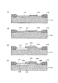
MOS型半導体素子において、例えば下記の非特許文献1に示されているように、ソース・ドレイン間耐圧を確保する手段として、ゲートフィールドプレート構造を採用している。ゲートフィールドプレート構造は、通常LOCOS法により形成したフィールド酸化膜の上部にゲート電極の端部が乗り上げるように形成する。これにより、ゲートオフ時の電界を分散させて耐圧を確保することができる。一般には、20V程度以上の耐圧を有する横型のMOS型半導体素子に適用される。
図11に、従来技術による半導体装置である横型二重拡散MOS(LDMOS)構造を示す。なお、図11において、シリコン基板10にはLOCOS法によって素子分離領域としてのフィールド酸化膜22が形成されている。シリコン基板10上にはゲート酸化膜24を介してゲート電極26が形成されている。このゲート電極26がフィールド酸化膜22に乗り上げた状態となっている。なお、符号28はボディ領域;30a,30bはソース・ドレイン領域;32はボディ領域からの引き出し領域;34はシリコン酸化膜;36はコンタクト;38はアルミ配線層を示す。
FIG. 11 shows a lateral double diffusion MOS (LDMOS) structure which is a semiconductor device according to the prior art. In FIG. 11, a
しかしながら、上記構成の半導体装置では、ゲート電極が乗り上げるフィールド酸化膜を、素子分離に用いる他のフィールド酸化膜と同時に形成するため、種々の問題が発生していた。 However, in the semiconductor device having the above configuration, various problems occur because the field oxide film on which the gate electrode rides is formed simultaneously with other field oxide films used for element isolation.
ゲート電極の一部が乗り上げているフィールド酸化膜22は、他のフィールド酸化膜(素子分離領域)22と同様に、例えば600nm程度の膜厚を有する。このうち300nm程度は、シリコン基板10の表面より下部に形成されたものである。このため、ソースおよびボディ領域28を接地し、ドレイン領域を正電圧印加の状態にした場合、シリコン基板10と接するフィールド酸化膜端部A(図中、破線の円で囲った部分)において電解集中が起こりやすく、耐圧低下の原因となっていた。
The
本発明は、上記のような状況に鑑みて成されたものであり、フィールド・プレート電極下の絶縁膜における電界集中を抑制可能な半導体装置を提供することを目的とする。 The present invention has been made in view of the above situation, and an object thereof is to provide a semiconductor device capable of suppressing electric field concentration in an insulating film under a field plate electrode.
また、本発明は、フィールド・プレート電極下の絶縁膜における電界集中を抑制可能な半導体装置の製造方法を提供することを他の目的とする。
Another object of the present invention is to provide a method of manufacturing a semiconductor device capable of suppressing electric field concentration in an insulating film under a field plate electrode.
本発明は、上記目的を達成するために、フィールド・プレート電極下の絶縁膜の端部形状を緩やかにしている。ここで、フィールド・プレート構造とは、トランジスタのゲート電極、ドレイン電極間の保護膜上にゲート電極と同電位のフィールド・プレート電極を形成して、動作時のゲート電極端での電界集中を緩和し高耐圧化、高出力化を可能とする構造である。 In the present invention, in order to achieve the above object, the end shape of the insulating film under the field plate electrode is made gentle. Here, the field plate structure means that a field plate electrode having the same potential as the gate electrode is formed on the protective film between the gate electrode and the drain electrode of the transistor, thereby mitigating electric field concentration at the gate electrode end during operation. However, this structure enables high breakdown voltage and high output.
本発明の第1の態様は、ゲートフィールドプレート構造を有する半導体装置において、半導体基板と;前記半導体基板上に形成されたゲート絶縁膜と;前記半導体基板上に形成された保護絶縁膜と;前記ゲート絶縁膜上に形成されたゲート電極と;前記保護絶縁膜上に形成され、前記ゲート電極と同電位のフィールド・プレート電極とを備える。そして、前記保護絶縁膜は、前記半導体基板の表面に形成され、当該基板内側には形成されない構造とすることを特徴とする。 According to a first aspect of the present invention, in a semiconductor device having a gate field plate structure, a semiconductor substrate; a gate insulating film formed on the semiconductor substrate; a protective insulating film formed on the semiconductor substrate; A gate electrode formed on the gate insulating film; and a field plate electrode formed on the protective insulating film and having the same potential as the gate electrode. The protective insulating film is formed on the surface of the semiconductor substrate and is not formed inside the substrate.
前記保護絶縁膜は、高密度プラズマCVD法や等方的なウェットエッチング法により成形することが好ましい。 The protective insulating film is preferably formed by a high density plasma CVD method or an isotropic wet etching method.
本発明の第2の態様は、LOCOS法による素子分離領域によって分離された領域内に形成された半導体装置において、半導体基板と;前記半導体基板上に形成されたゲート絶縁膜と;LOCOS法によって前記半導体基板上に形成された保護絶縁膜と;前記ゲート絶縁膜上に形成されたゲート電極と;前記保護絶縁膜上に形成され、前記ゲート電極と同電位のフィールド・プレート電極とを備える。そして、前記保護絶縁膜は、前記素子分離領域よりも薄く成形されることを特徴とする。 According to a second aspect of the present invention, there is provided a semiconductor device formed in a region isolated by an element isolation region by a LOCOS method; a semiconductor substrate; a gate insulating film formed on the semiconductor substrate; and the LOCOS method. A protective insulating film formed on the semiconductor substrate; a gate electrode formed on the gate insulating film; and a field plate electrode formed on the protective insulating film and having the same potential as the gate electrode. The protective insulating film is formed thinner than the element isolation region.
本発明の第3の態様は、ゲートフィールドプレート構造を有する半導体装置の製造方法において、半導体基板上に高密度プラズマCVD法によって保護絶縁膜を形成する工程と;前記半導体基板上にゲート絶縁膜を形成する工程と;前記ゲート絶縁膜及び前記保護絶縁膜上にゲート電極を形成する工程とを含むことを特徴とする。 According to a third aspect of the present invention, in the method for manufacturing a semiconductor device having a gate field plate structure, a protective insulating film is formed on a semiconductor substrate by a high-density plasma CVD method; and a gate insulating film is formed on the semiconductor substrate. Forming a gate electrode on the gate insulating film and the protective insulating film.
本発明の第4の態様は、ゲートフィールドプレート構造を有する半導体装置の製造方法において、半導体基板上に等方性ウェットエッチング法によって保護絶縁膜を形成する工程と;前記半導体基板上にゲート絶縁膜を形成する工程と;前記ゲート絶縁膜及び前記保護絶縁膜上にゲート電極を形成する工程とを含むことを特徴とする。 According to a fourth aspect of the present invention, there is provided a method of manufacturing a semiconductor device having a gate field plate structure, the step of forming a protective insulating film on a semiconductor substrate by an isotropic wet etching method; and a gate insulating film on the semiconductor substrate. And a step of forming a gate electrode on the gate insulating film and the protective insulating film.
本発明の第5の態様は、ゲートフィールドプレート構造を有する半導体装置の製造方法において、半導体基板上にLOCOS法によって素子分離領域及び保護絶縁膜を形成する工程と;前記半導体基板上にゲート絶縁膜を形成する工程と;前記ゲート絶縁膜及び前記保護絶縁膜上にゲート電極を形成する工程とを含む。そして、前記保護絶縁膜は、前記素子分離領域よりも薄く成形することを特徴とする。
According to a fifth aspect of the present invention, in the method for manufacturing a semiconductor device having a gate field plate structure, a step of forming an element isolation region and a protective insulating film on a semiconductor substrate by a LOCOS method; and a gate insulating film on the semiconductor substrate Forming a gate electrode on the gate insulating film and the protective insulating film. The protective insulating film is formed thinner than the element isolation region.
本発明の何れの態様においても、フィールド・プレート電極下の絶縁膜の端部形状を緩やかにすることができ、フィールド・プレート電極下の絶縁膜の端部で発生する電界集中を効果的に抑制可能となる。その結果、半導体装置の耐圧低下を抑制することができる。 In any aspect of the present invention, the shape of the end of the insulating film under the field plate electrode can be relaxed, and the electric field concentration generated at the end of the insulating film under the field plate electrode can be effectively suppressed. It becomes possible. As a result, a decrease in breakdown voltage of the semiconductor device can be suppressed.
上述した本発明の第1及び第3の態様によれば、ゲートフィールドプレート下の保護絶縁膜がシリコン基板内部に形成されず、シリコン基板表面の平坦性が保たれる。また、保護絶縁膜は端部の傾斜が緩く、ゲート電極下の保護膜厚が急激に変化することが無い。更に、保護絶縁膜の膜厚を素子分離のためのフィールド酸化膜厚とは独立に決めることができ、最良の条件で電解を分散させることができる。その結果、従来に見られるような酸化膜端部での電解集中による耐圧低下を防ぐことが可能となる。 According to the first and third aspects of the present invention described above, the protective insulating film under the gate field plate is not formed inside the silicon substrate, and the flatness of the silicon substrate surface is maintained. Further, the protective insulating film has a gentle slope at the end, and the protective film thickness under the gate electrode does not change abruptly. Furthermore, the film thickness of the protective insulating film can be determined independently of the field oxide film thickness for element isolation, and electrolysis can be dispersed under the best conditions. As a result, it is possible to prevent a decrease in breakdown voltage due to electrolytic concentration at the end of the oxide film as seen conventionally.
ここで、本発明の第3の態様のように、保護絶縁膜を半導体基板上に形成する際に、等方性ウェットエッチング法を採用した場合には、シリコンのエピタキシャル成長法や高密度プラズマCVD法を用いる必要が無く、低コストでの保護絶縁膜の形成が可能となる。 Here, as in the third aspect of the present invention, when the isotropic wet etching method is employed when the protective insulating film is formed on the semiconductor substrate, the silicon epitaxial growth method or the high-density plasma CVD method is used. Therefore, it is possible to form a protective insulating film at low cost.
一方、上述した本発明の第2及び第5の態様によれば、保護絶縁膜を素子分離領域と同様にLOCOS法によって形成するが、保護絶縁膜の方が厚さが薄く、バーズビークの形状が緩やかになる。このため、従来に比べて半導体基板表面の平坦性が保たれ、保護絶縁膜の端部での電解集中による耐圧低下を防ぐことが可能となる。また、一度のフォトリソグラフィー工程により異なる膜厚を有するフィールド酸化膜を形成することが可能となり、製造コストの増大を抑制することができる。
On the other hand, according to the above-described second and fifth aspects of the present invention, the protective insulating film is formed by the LOCOS method in the same manner as the element isolation region. Be gentle. For this reason, the flatness of the surface of the semiconductor substrate is maintained as compared with the conventional case, and it is possible to prevent a decrease in breakdown voltage due to electrolytic concentration at the end of the protective insulating film. In addition, field oxide films having different film thicknesses can be formed by a single photolithography process, and an increase in manufacturing cost can be suppressed.
以下、本発明を実施するための最良の形態について、実施例を用いて詳細に説明する。 Hereinafter, the best mode for carrying out the present invention will be described in detail using embodiments.
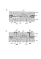
(第1の実施例)
本発明の第1の実施例に係る半導体装置は、ゲートフィールドプレート構造を有する。後に説明するように、ゲート電極の一部が乗り上げているシリコン酸化膜(保護絶縁)がLOCOS酸化法以外の方法によって形成され、シリコン基板表面の平坦性が保たれている。さらに、シリコン酸化膜(保護絶縁膜)の端部の傾斜が緩く、ゲート電極下の酸化膜厚が急激に変化しないことを特徴とする。
(First embodiment)
The semiconductor device according to the first embodiment of the present invention has a gate field plate structure. As will be described later, a silicon oxide film (protective insulation) on which a part of the gate electrode rides is formed by a method other than the LOCOS oxidation method, and the flatness of the silicon substrate surface is maintained. Furthermore, the inclination of the end of the silicon oxide film (protective insulating film) is gentle, and the oxide film thickness under the gate electrode does not change abruptly.
図1(A)〜(D)、図2(E)〜(H)、図3(I)〜(L)、図4(M)〜(N)は、本発明の第1の実施例に係る半導体装置となるLDMOS(横方向拡散MOS)の製造工程を示す。 1 (A) to (D), FIGS. 2 (E) to (H), FIGS. 3 (I) to (L), and FIGS. 4 (M) to (N) are the first embodiment of the present invention. A manufacturing process of an LDMOS (lateral diffusion MOS) serving as the semiconductor device will be described.
まず、図1(A)に示すように、N型シリコン基板10上にフォトレジスト112をフォトリソグラフィー技術によりパターニングする。
First, as shown in FIG. 1A, a
次に、図1(B)に示すように、フォトレジスト112をマスクとしたエッチングにより、N型シリコン基板10に深さ500nm程度の溝(段差)114を形成する。溝114の形成位置は、保護絶縁膜を形成する領域を規制する周囲の領域である。
Next, as shown in FIG. 1B, a groove (step) 114 having a depth of about 500 nm is formed in the N-
その後、図1(C)に示すように、シリコン基板10上のフォトレジスト112を除去する。
Thereafter, as shown in FIG. 1C, the
次に、図1(D)に示すように、高密度プラズマCVD法により、シリコン基板110の全面にシリコン酸化膜(116a,116b)を300nm程度堆積する。この時、溝114を形成していないシリコン基板110の表面には、端部の堆積角度を(垂直に対して)約60°に保った形でシリコン酸化膜116aが形成される。また、シリコン酸化膜116aとは分離して、溝114の底部にはシリコン酸化膜116bが形成される。
Next, as shown in FIG. 1D, a silicon oxide film (116a, 116b) is deposited to a thickness of about 300 nm on the entire surface of the
ここで、高密度プラズマCVD工程においては、例えば、プラズマ処理チャンバー側に掛かるデポジションパワー(A=4kW)と、処理基板側に掛かるスパッタパワー(B=3kW)との比(A:B)が約4:3とすることが好ましい。また、基板温度は700℃程度が好ましい。 Here, in the high-density plasma CVD process, for example, the ratio (A: B) of the deposition power (A = 4 kW) applied to the plasma processing chamber side and the sputtering power (B = 3 kW) applied to the processing substrate side is It is preferably about 4: 3. The substrate temperature is preferably about 700 ° C.
次に、図2(E)に示すように、シリコン酸化膜116aを覆うように、フォトリソグラフィー法によりフォトレジスト118を形成する。
Next, as shown in FIG. 2E, a
次に、図2(F)に示すように、フォトレジスト118をマスクとして、溝114の底部のシリコン酸化膜116bを除去する。
Next, as shown in FIG. 2F, the
その後、図2(G)に示すように、シリコン酸化膜116a上のフォトレジスト118を除去する。なお、図1(D)に示すシリコン酸化膜(116a,116b)の形成工程において、密度の低い通常のプラズマCVDを採用した場合には、シリコン酸化膜116aと116bとが繋がってしまい、段差部の側面にもシリコン酸化膜が形成されることとなる。その結果、フォトレジスト118を除去した後も、段差部の側面にシリコン酸化膜が残ってしまうという不都合が生じる。
Thereafter, as shown in FIG. 2G, the
次に、図2(H)に示すように、エピタキシャル法によりシリコン基板110と同濃度のシリコン120を、シリコン基板110の表面まで成長させ、シリコン基板110の表面を平坦にする。
Next, as shown in FIG. 2H,
次に、図3(I)に示すように、通常のLOCOS法により、膜厚600nm程度の素子分離のためのフィールド酸化膜122を、シリコン基板110上に形成する。
Next, as shown in FIG. 3I, a
次に、図3(J)に示すように、熱酸化法により20nmのゲート酸化膜124をシリコン基板110上に形成する。
Next, as shown in FIG. 3J, a 20 nm
次に、不純物としてリンを含んだ多結晶シリコンをシリコン基板110上に300nmの膜厚で堆積した後、フォトリソグラフィー・エッチング法により、図3(K)に示すように、ゲート電極126を形成する。ゲート電極126は、ゲート酸化膜124のみならず、シリコン酸化膜(保護絶縁膜)112aの上に形成される。これによって、ゲートフィールドプレート構造が形成される。
Next, after depositing polycrystalline silicon containing phosphorus as an impurity to a thickness of 300 nm on the
次に、フォトリソグラフィー・イオン注入法により、ボロンをシリコン基板110の所望の領域に注入し、さらに1100℃、60分程度の熱処理により拡散・活性化させることにより、図3(K)に示すボディ領域128を形成する。
Next, boron is implanted into a desired region of the
更に、2度のフォトリソグラフィー・イオン注入法により、ヒ素およびボロンをシリコン基板110の所望の領域に注入し、それに引き続く900℃、30分程度の熱処理で活性化させることにより、図3(L)に示すように、ソース・ドレイン領域130a,130b及び、ボディ領域128からの引き出し領域132を形成する。
Further, arsenic and boron are implanted into a desired region of the
次に、図4(M)に示すように、CVD法により全面にシリコン酸化膜134を1μm程度堆積し、平坦化する。
Next, as shown in FIG. 4M, a
その後、図4(N)に示すように、通常の方法により、ソース・ドレイン領域130a、130bに接続されたコンタクト136をシリコン酸化膜134中に形成する。また、シリコン酸化膜134の表面においてコンタクト136と接続されるアルミ配線層138を形成する。
Thereafter, as shown in FIG. 4N,
本実施例に係る半導体装置の動作は、通常のゲートフィールドプレート構造を有するLDMOSと同様である。即ち、ソースおよびボディ領域128を接地、ドレイン領域を耐圧以下の正電圧印加の状態で、ゲート電極126に閾値以上の電圧を印加する。これにより、ボディ層表面を反転させてチャネルが形成され、電流がドレインからソースへと流れる。このようなゲート電極126への電圧印加を繰り返すことにより、LDMOSはスイッチング動作を行う。ゲートオフ時には、ゲートフィールドプレート構造により電界を分散させて耐圧を確保することができる。
The operation of the semiconductor device according to the present embodiment is the same as that of an LDMOS having a normal gate field plate structure. That is, a voltage higher than the threshold value is applied to the
以上のように第1の実施例によれば、ゲートフィールドプレート(126)下の酸化膜116aがシリコン基板110内部に形成されておらず、シリコン基板110表面の平坦性が保たれる。また、この酸化膜116aは端部の傾斜が緩く、厚みが急激に変化することが無い。更に、保護絶縁膜としてのシリコン酸化膜116aの膜厚を、素子分離のためのフィールド酸化膜122の膜厚とは独立に決めることができる。このため、最良の条件で電解を分散させることができ、従来技術に見られるような酸化膜端部での電解集中による耐圧低下を防ぐことが可能となる。
As described above, according to the first embodiment, the
(第2の実施例)
本発明の第2の実施例に係る半導体装置は、上述した第1の実施例と同様にゲートフィールドプレート構造を有する。後に説明するように、ゲート電極の一部が乗り上げているシリコン酸化膜(保護絶縁膜)がLOCOS酸化法以外の方法によって形成され、シリコン基板表面の平坦性が保たれている。さらに、シリコン酸化膜(保護絶縁膜)の端部の傾斜が緩く、ゲート電極下の酸化膜厚が急激に変化しないことを特徴とする。
(Second embodiment)
The semiconductor device according to the second embodiment of the present invention has a gate field plate structure as in the first embodiment described above. As will be described later, a silicon oxide film (protective insulating film) on which a part of the gate electrode rides is formed by a method other than the LOCOS oxidation method, and the flatness of the silicon substrate surface is maintained. Furthermore, the inclination of the end of the silicon oxide film (protective insulating film) is gentle, and the oxide film thickness under the gate electrode does not change abruptly.
図5(A)〜(D)、図6(E)〜(H)、図7(I)〜(J)は、本発明の第2の実施例に係る半導体装置となるLDMOS(横方向拡散MOS)の製造工程を示す。 FIGS. 5A to 5D, FIGS. 6E to 6H, and FIGS. 7I to 7J illustrate an LDMOS (lateral diffusion) which is a semiconductor device according to the second embodiment of the present invention. The manufacturing process of MOS) is shown.
まず、図5(A)に示すように、N型シリコン基板210上にCVD法により、300nmの厚さのシリコン酸化膜212を形成する。
First, as shown in FIG. 5A, a 300 nm-thickness
次に、図5(B)に示すように、シリコン酸化膜212上にCVD法により、300nmの厚さのシリコン窒化膜214を形成する。
Next, as shown in FIG. 5B, a
次に、フォトリソグラフィー及びエッチング処理により、図5(C)に示すように、保護絶縁膜(ゲートフィールドプレート下の酸化膜)に相当する領域のシリコン窒化膜214をマスク214aとして残す。
Next, as shown in FIG. 5C, the
次に、残されたシリコン窒化膜214aをマスクとして、ウェットエッチング法によりシリコン酸化膜212を等方的に除去する。当方的なエッチングにより、シリコン酸化膜212の端部は、図5(D)に示すように、内側に湾曲した形状となる。
Next, the
次に、図6(E)に示すように、通常のLOCOS法により、シリコン基板210上に膜厚600nm程度の素子分離のためのフィールド酸化膜222を形成する。
Next, as shown in FIG. 6E, a
次に、図6(F)に示すように、熱酸化法により20nmのゲート酸化膜224を、シリコン基板210上に形成する。
Next, as shown in FIG. 6F, a 20 nm
次に、不純物としてリンを含んだ多結晶シリコンを、シリコン基板210上に300nm堆積した後、フォトリソグラフィー・エッチング法により、図6(G)に示すように、ゲート電極226を形成する。ゲート電極226は、ゲート酸化膜224のみならず、シリコン酸化膜(保護絶縁膜)212aの上に形成される。これによって、ゲートフィールドプレート構造が形成される。
Next, after depositing 300 nm of polycrystalline silicon containing phosphorus as an impurity on the
次に、フォトリソグラフィー・イオン注入法により、ボロンをシリコン基板210の所望の領域に注入し、さらに1100℃、60分程度の熱処理により拡散・活性化させることにより、図6(G)に示すボディ領域228を形成する。
Next, boron is implanted into a desired region of the
更に、2度のフォトリソグラフィー・イオン注入法により、ヒ素およびボロンをシリコン基板210の所望の領域に注入し、それに引き続く900℃、30分程度の熱処理で活性化させることにより、図6(H)に示すように、ソース・ドレイン領域230a,230b及び、ボディ領域228からの引き出し領域232を形成する。
Further, arsenic and boron are implanted into a desired region of the
次に、図7(I)に示すように、CVD法により全面にシリコン酸化膜234を1μm程度堆積し、平坦化する。
Next, as shown in FIG. 7I, a
その後、図7(J)に示すように、通常の方法により、ソース・ドレイン領域230a、230bに接続されたコンタクト236をシリコン酸化膜234中に形成する。また、シリコン酸化膜234の表面においてコンタクト236と接続されるアルミ配線層238を形成する。
Thereafter, as shown in FIG. 7J,
本実施例に係る半導体装置の動作は、上述した第1の実施例と同様である。即ち、ソースおよびボディ領域228を接地、ドレイン領域を耐圧以下の正電圧印加の状態で、ゲート電極226に閾値以上の電圧を印加する。これにより、ボディ層表面を反転させてチャネルが形成され、電流がドレインからソースへと流れる。このようなゲート電極226への電圧印加を繰り返すことにより、LDMOSはスイッチング動作を行う。ゲートオフ時には、ゲートフィールドプレート構造により電界を分散させて耐圧を確保することができる。
The operation of the semiconductor device according to this embodiment is the same as that of the first embodiment described above. That is, a voltage higher than the threshold is applied to the
以上のように第2の実施例によれば、ゲートフィールドプレート(226)下の酸化膜212aがシリコン基板210内部に形成されず、シリコン基板210表面の平坦性が保たれる。また、この酸化膜212aは端部の傾斜が緩く、厚みが急激に変化することが無い。更に、保護絶縁膜としてのシリコン酸化膜1212aの膜厚を、素子分離のためのフィールド酸化膜222の膜厚とは独立に決めることができる。このため、最良の条件で電解を分散させることができ、従来技術に見られるような酸化膜端部での電解集中による耐圧低下を防ぐことが可能となる。
As described above, according to the second embodiment, the
加えて、本発明の第2の実施例によれば、保護酸化膜(212a)を形成するのにシリコンのエピタキシャル成長法や高密度プラズマCVD法を用いる必要が無い。このため、第1の実施例よりも低コストで半導体装置を製造することが可能となる。
In addition, according to the second embodiment of the present invention, it is not necessary to use a silicon epitaxial growth method or a high-density plasma CVD method to form the protective oxide film (212a). For this reason, it becomes possible to manufacture a semiconductor device at a lower cost than in the first embodiment.
(第3の実施例)
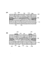
本発明の第3実施例に係る半導体装置は、上述した第1、第2の実施例と同様にゲートフィールドプレート構造を有する。後に説明するように、ゲート電極の一部が乗り上げているシリコン酸化膜がLOCOS酸化法により形成されるが、他の素子分離のためのフィールド酸化膜よりも薄くなっている。このため、従来の構造に比べてシリコン基板表面の平坦性が保たれている。さらに、シリコン酸化膜(保護絶縁膜)の端部の傾斜が緩く、ゲート電極下の酸化膜厚が急激に変化しないことを特徴とする。
(Third embodiment)
The semiconductor device according to the third embodiment of the present invention has a gate field plate structure as in the first and second embodiments described above. As will be described later, the silicon oxide film on which a part of the gate electrode rides is formed by the LOCOS oxidation method, but is thinner than the field oxide film for other element isolation. For this reason, the flatness of the silicon substrate surface is maintained as compared with the conventional structure. Furthermore, the inclination of the end of the silicon oxide film (protective insulating film) is gentle, and the oxide film thickness under the gate electrode does not change abruptly.
図8(A)〜(D)、図9(E)〜(G)、図10(H)〜(I)は、本発明の第3の実施例に係る半導体装置となるLDMOS(横方向拡散MOS)の製造工程を示す。 FIGS. 8A to 8D, FIGS. 9E to 10G, and FIGS. 10H to 10I illustrate LDMOSs (transverse diffusions) that are semiconductor devices according to the third embodiment of the present invention. The manufacturing process of MOS) is shown.
まず、図8(A)に示すように、N型シリコン基板310上に熱酸化法によりシリコン酸化膜312を50nmの厚さで形成する。
First, as shown in FIG. 8A, a
次に、図8(B)に示すように、シリコン酸化膜312上にCVD法によりシリコン窒化膜314を200nmの厚さで堆積する。
Next, as shown in FIG. 8B, a
次に、図8(C)に示すように、フォトリソグラフィー・エッチング法により、最終的にフィールド酸化膜となる領域のシリコン窒化膜314を除去し、マスクパターン314aを形成する。この時、ゲートフィールドプレート下のシリコン酸化膜が形成される領域においては、0.2μm幅のライン・アンド・スペースで溝315を形成する。なお、溝315はライン・アンド・スペースでなく、ドット状、マトリックス状など他の形状を採用することができる。
Next, as shown in FIG. 8C, the
次に、シリコン窒化膜314aをマスクとして、1000℃の熱酸化法により、露出したシリコン基板表面を酸化して膜厚600nm程度の厚いフィールド酸化膜322を形成する。この時、溝315に挟まれた領域もある程度酸化されることにより、ゲートフィールドプレートが形成される領域においては、膜厚300nm程度の薄いフィールド酸化膜322aが形成される。その後、図8(D)に示すように、エッチング法によりシリコン窒化膜314とシリコン酸化膜312をシリコン基板310から除去する。
Next, using the
次に、図9(E)に示すように、熱酸化法により20nmのゲート酸化膜324をシリコン基板310上に形成する。
Next, as shown in FIG. 9E, a 20 nm
次に、不純物としてリンを含んだ多結晶シリコンを、シリコン基板310上に300nm堆積した後、フォトリソグラフィー・エッチング法により、図9(F)に示すように、ゲート電極326を形成する。ゲート電極326は、ゲート酸化膜324のみならず、フィールド酸化膜(保護絶縁膜)332aの上に形成される。これによって、ゲートフィールドプレート構造が形成される。
Next, after depositing 300 nm of polycrystalline silicon containing phosphorus as an impurity on the
次に、フォトリソグラフィー・イオン注入法により、ボロンをシリコン基板310の所望の領域に注入し、さらに1100℃、60分程度の熱処理により拡散・活性化させることにより、図9(F)に示すボディ領域328を形成する。
Next, boron is implanted into a desired region of the
更に、2度のフォトリソグラフィー・イオン注入法により、ヒ素およびボロンを所望の領域に注入し、それに引き続く900℃、30分程度の熱処理で活性化させることにより、図9(G)に示すように、ソース・ドレイン領域330a,330b及び、ボディ領域328からの引き出し領域332を形成する。
Further, arsenic and boron are implanted into a desired region by photolithography ion implantation twice, and then activated by heat treatment at 900 ° C. for about 30 minutes, as shown in FIG. 9 (G). Source /
次に、図10(H)に示すように、CVD法により全面にシリコン酸化膜334を1μm程度堆積し、平坦化する。
Next, as shown in FIG. 10H, a
その後、図10(I)に示すように、通常の方法により、ソース・ドレイン領域330a、330bに接続されたコンタクト336をシリコン酸化膜334中に形成する。また、シリコン酸化膜334の表面においてコンタクト336と接続されるアルミ配線層338を形成する。
Thereafter, as shown in FIG. 10I,
本実施例に係る半導体装置の動作は、上述した第1及び第2の実施例と同様である。即ち、ソースおよびボディ領域328を接地、ドレイン領域を耐圧以下の正電圧印加の状態で、ゲート電極326に閾値以上の電圧を印加する。これにより、ボディ層表面を反転させてチャネルが形成され、電流がドレインからソースへと流れる。このようなゲート電極326への電圧印加を繰り返すことにより、LDMOSはスイッチング動作を行う。ゲートオフ時には、ゲートフィールドプレート構造により電界を分散させて耐圧を確保することができる。
The operation of the semiconductor device according to this embodiment is the same as that of the first and second embodiments described above. That is, a voltage higher than the threshold is applied to the
以上のように本発明の第3の実施例によれば、ゲートフィールドプレート下の保護絶縁膜を素子分離領域と同様にLOCOS法によって形成するが、保護絶縁膜の方が厚さが薄く、バーズビークの形状が緩やかになる。このため、従来の構造以上にシリコン基板表面の平坦性が確保される。その結果、保護絶縁膜の端部での電解集中による耐圧低下を防ぐことが可能となる。
また、一度のフォトリソグラフィー工程により異なる膜厚を有するフィールド酸化膜(322,322a)を形成することができるため、製造コストの増大を抑制することができる。
As described above, according to the third embodiment of the present invention, the protective insulating film under the gate field plate is formed by the LOCOS method in the same manner as the element isolation region. However, the protective insulating film is thinner and has a bird's beak. The shape of the. For this reason, the flatness of the silicon substrate surface is ensured more than the conventional structure. As a result, it is possible to prevent a decrease in breakdown voltage due to electrolytic concentration at the end of the protective insulating film.
In addition, since field oxide films (322, 322a) having different film thicknesses can be formed by a single photolithography process, an increase in manufacturing cost can be suppressed.
以上、本発明の実施例について説明したが、本発明は特許請求の範囲に記載された技術的思想の範囲内において、適宜設計変更が可能である。
The embodiments of the present invention have been described above, but the present invention can be appropriately modified within the scope of the technical idea described in the claims.
110,210,310 シリコン基板
114 溝
116a,212a シリコン酸化膜(保護絶縁膜)
122,222,322 LOCOS酸化膜(素子分離領域)
124,224,324 ゲート酸化膜
126,226,326 ゲート電極
322a LOCOS酸化膜(保護絶縁膜)
110, 210, 310
122, 222, 322 LOCOS oxide film (element isolation region)
124, 224, 324
Claims (5)
前記保護絶縁膜形成領域の周囲の前記半導体基板の表面に溝を形成する工程と、
前記溝を形成した後に、前記保護絶縁膜形成領域上に高密度プラズマCVD法によって絶縁膜を堆積してテーパー形状の保護絶縁膜を形成する工程と、
前記溝を前記半導体基板と同一導電型の半導体層で埋め込む工程と、
前記半導体層の表面に、前記保護絶縁膜に接続され前記半導体層の表面からの膜厚が前記保護絶縁膜よりも薄いゲート絶縁膜を形成する工程と、
前記ゲート絶縁膜上及び前記保護絶縁膜上に跨るゲート電極を形成する工程と、を有することを特徴とする半導体装置の製造方法。 Preparing a semiconductor substrate having a protective insulating film formation region on the surface;
Forming a groove in the surface of the semiconductor substrate around the protective insulating film formation region;
After forming the groove, a step of depositing an insulating film on the protective insulating film forming region by a high density plasma CVD method to form a tapered protective insulating film;
Filling the groove with a semiconductor layer of the same conductivity type as the semiconductor substrate;
Forming on the surface of the semiconductor layer a gate insulating film connected to the protective insulating film and having a film thickness from the surface of the semiconductor layer thinner than the protective insulating film;
Forming a gate electrode straddling over the gate insulating film and the protective insulating film.
前記保護絶縁膜形成領域の周囲の前記半導体基板の表面に溝を形成する工程と、
前記溝を形成した後に、前記保護絶縁膜形成領域上及び前記溝の底面に高密度プラズマCVD法によって絶縁膜を堆積してテーパー形状の保護絶縁膜を形成する工程と、
前記溝の底面に形成された前記絶縁膜を除去する工程と、
前記溝を前記半導体基板と同一導電型の半導体層で埋め込む工程と、
前記半導体層の表面に、前記保護絶縁膜に接続され前記半導体層の表面からの膜厚が前記保護絶縁膜よりも薄いゲート絶縁膜を形成する工程と、
前記ゲート絶縁膜上及び前記保護絶縁膜上に跨るゲート電極を形成する工程と、を有することを特徴とする半導体装置の製造方法。
Preparing a semiconductor substrate having a protective insulating film formation region on the surface;
Forming a groove in the surface of the semiconductor substrate around the protective insulating film formation region;
Forming a tapered protective insulating film by forming an insulating film on the protective insulating film forming region and on the bottom surface of the groove by high-density plasma CVD after forming the groove;
Removing the insulating film formed on the bottom surface of the groove;
Filling the groove with a semiconductor layer of the same conductivity type as the semiconductor substrate;
Forming on the surface of the semiconductor layer a gate insulating film connected to the protective insulating film and having a film thickness from the surface of the semiconductor layer thinner than the protective insulating film;
Forming a gate electrode straddling over the gate insulating film and the protective insulating film.
Priority Applications (2)
| Application Number | Priority Date | Filing Date | Title |
|---|---|---|---|
| JP2006262373A JP4611270B2 (en) | 2006-09-27 | 2006-09-27 | Manufacturing method of semiconductor device |
| US11/892,729 US20080073746A1 (en) | 2006-09-27 | 2007-08-27 | Semiconductor device |
Applications Claiming Priority (1)
| Application Number | Priority Date | Filing Date | Title |
|---|---|---|---|
| JP2006262373A JP4611270B2 (en) | 2006-09-27 | 2006-09-27 | Manufacturing method of semiconductor device |
Related Child Applications (1)
| Application Number | Title | Priority Date | Filing Date |
|---|---|---|---|
| JP2009169715A Division JP4657356B2 (en) | 2009-07-21 | 2009-07-21 | Manufacturing method of semiconductor device |
Publications (2)
| Publication Number | Publication Date |
|---|---|
| JP2008085031A JP2008085031A (en) | 2008-04-10 |
| JP4611270B2 true JP4611270B2 (en) | 2011-01-12 |
Family
ID=39224039
Family Applications (1)
| Application Number | Title | Priority Date | Filing Date |
|---|---|---|---|
| JP2006262373A Expired - Fee Related JP4611270B2 (en) | 2006-09-27 | 2006-09-27 | Manufacturing method of semiconductor device |
Country Status (2)
| Country | Link |
|---|---|
| US (1) | US20080073746A1 (en) |
| JP (1) | JP4611270B2 (en) |
Families Citing this family (11)
| Publication number | Priority date | Publication date | Assignee | Title |
|---|---|---|---|---|
| JP5388500B2 (en) * | 2007-08-30 | 2014-01-15 | 株式会社半導体エネルギー研究所 | Method for manufacturing semiconductor device |
| JP5371358B2 (en) * | 2008-09-29 | 2013-12-18 | ローム株式会社 | Semiconductor device and manufacturing method of semiconductor device |
| US9484454B2 (en) | 2008-10-29 | 2016-11-01 | Tower Semiconductor Ltd. | Double-resurf LDMOS with drift and PSURF implants self-aligned to a stacked gate “bump” structure |
| US9330979B2 (en) * | 2008-10-29 | 2016-05-03 | Tower Semiconductor Ltd. | LDMOS transistor having elevated field oxide bumps and method of making same |
| DE102011087845B4 (en) * | 2011-12-06 | 2015-07-02 | Infineon Technologies Ag | LATERAL TRANSISTOR COMPONENT AND METHOD FOR THE PRODUCTION THEREOF |
| US9136349B2 (en) * | 2012-01-06 | 2015-09-15 | Taiwan Semiconductor Manufacturing Company, Ltd. | Dummy gate structure for semiconductor devices |
| US8878275B2 (en) | 2013-02-18 | 2014-11-04 | Fairchild Semiconductor Corporation | LDMOS device with double-sloped field plate |
| JP6229646B2 (en) * | 2013-12-20 | 2017-11-15 | 株式会社デンソー | Semiconductor device |
| CN105374686A (en) * | 2014-09-02 | 2016-03-02 | 无锡华润上华半导体有限公司 | Method for manufacturing LDMOS device |
| US10014408B1 (en) * | 2017-05-30 | 2018-07-03 | Vanguard International Semiconductor Corporation | Semiconductor devices and methods for forming the same |
| DE102020117171A1 (en) | 2020-06-30 | 2021-12-30 | Infineon Technologies Dresden GmbH & Co. KG | LATERAL TRANSISTOR WITH SELF-ALIGNING BODY IMPLANT |
Citations (6)
| Publication number | Priority date | Publication date | Assignee | Title |
|---|---|---|---|---|
| JPH01274457A (en) * | 1988-04-26 | 1989-11-02 | Seiko Instr Inc | Manufacture of semiconductor device |
| JPH01293668A (en) * | 1988-05-23 | 1989-11-27 | Seiko Instr Inc | Manufacture of insulated-gate field-effect transistor |
| JPH0582783A (en) * | 1991-03-22 | 1993-04-02 | Philips Gloeilampenfab:Nv | Lateral insulated-gate field-effect semiconductor device |
| JPH06232156A (en) * | 1993-01-29 | 1994-08-19 | Ricoh Co Ltd | Semiconductor device and manufacture thereof |
| JP2002176173A (en) * | 2000-12-07 | 2002-06-21 | Sanyo Electric Co Ltd | Semiconductor device and manufacturing method therefor |
| JP2002314065A (en) * | 2001-04-13 | 2002-10-25 | Sanyo Electric Co Ltd | Mos semiconductor device and its manufacturing method |
Family Cites Families (5)
| Publication number | Priority date | Publication date | Assignee | Title |
|---|---|---|---|---|
| US5072267A (en) * | 1989-06-28 | 1991-12-10 | Nec Corporation | Complementary field effect transistor |
| JP3206026B2 (en) * | 1991-07-19 | 2001-09-04 | 富士電機株式会社 | Semiconductor device having high voltage MISFET |
| JP3000739B2 (en) * | 1991-08-22 | 2000-01-17 | 日本電気株式会社 | Vertical MOS field effect transistor and method of manufacturing the same |
| JP3673231B2 (en) * | 2002-03-07 | 2005-07-20 | 三菱電機株式会社 | Insulated gate semiconductor device and method of manufacturing gate wiring structure |
| US7719054B2 (en) * | 2006-05-31 | 2010-05-18 | Advanced Analogic Technologies, Inc. | High-voltage lateral DMOS device |
-
2006
- 2006-09-27 JP JP2006262373A patent/JP4611270B2/en not_active Expired - Fee Related
-
2007
- 2007-08-27 US US11/892,729 patent/US20080073746A1/en not_active Abandoned
Patent Citations (6)
| Publication number | Priority date | Publication date | Assignee | Title |
|---|---|---|---|---|
| JPH01274457A (en) * | 1988-04-26 | 1989-11-02 | Seiko Instr Inc | Manufacture of semiconductor device |
| JPH01293668A (en) * | 1988-05-23 | 1989-11-27 | Seiko Instr Inc | Manufacture of insulated-gate field-effect transistor |
| JPH0582783A (en) * | 1991-03-22 | 1993-04-02 | Philips Gloeilampenfab:Nv | Lateral insulated-gate field-effect semiconductor device |
| JPH06232156A (en) * | 1993-01-29 | 1994-08-19 | Ricoh Co Ltd | Semiconductor device and manufacture thereof |
| JP2002176173A (en) * | 2000-12-07 | 2002-06-21 | Sanyo Electric Co Ltd | Semiconductor device and manufacturing method therefor |
| JP2002314065A (en) * | 2001-04-13 | 2002-10-25 | Sanyo Electric Co Ltd | Mos semiconductor device and its manufacturing method |
Also Published As
| Publication number | Publication date |
|---|---|
| US20080073746A1 (en) | 2008-03-27 |
| JP2008085031A (en) | 2008-04-10 |
Similar Documents
| Publication | Publication Date | Title |
|---|---|---|
| JP4611270B2 (en) | Manufacturing method of semiconductor device | |
| JP7279277B2 (en) | Multiple shield trench gate FET | |
| US9673289B2 (en) | Dual oxide trench gate power MOSFET using oxide filled trench | |
| JP6106310B2 (en) | Hybrid active field gap extended drain MOS transistor | |
| JP4928947B2 (en) | Manufacturing method of super junction device | |
| JP5198752B2 (en) | Manufacturing method of semiconductor device | |
| JP5298565B2 (en) | Semiconductor device and manufacturing method thereof | |
| JP6666671B2 (en) | Semiconductor device | |
| JP2006196518A (en) | Semiconductor device and its fabrication process | |
| JP2008153685A (en) | Method for manufacturing semiconductor device | |
| JP2005510088A (en) | Trench metal oxide semiconductor field effect transistor device with polycrystalline silicon source contact structure | |
| JP2009130357A (en) | Trench mosfet and manufacturing method thereof | |
| JP4657356B2 (en) | Manufacturing method of semiconductor device | |
| JP2006229181A (en) | Semiconductor device | |
| JP2024032949A (en) | Manufacturing method of semiconductor device | |
| JP5371358B2 (en) | Semiconductor device and manufacturing method of semiconductor device | |
| JP2009065150A (en) | Trench transistor, and its formation method | |
| KR100680429B1 (en) | Method for fabricating semiconductor device | |
| JP2004158680A (en) | Semiconductor device and its fabricating process | |
| JP2008085205A (en) | Semiconductor device and its manufacturing method | |
| TWI750375B (en) | Trench gate mosfet and method of forming the same | |
| US7723784B2 (en) | Insulated gate semiconductor device and method for manufacturing the same | |
| JP2005252204A (en) | Insulating gate type semiconductor device and method of manufacturing the same | |
| JP5479671B2 (en) | Semiconductor device | |
| JP2010027680A (en) | Semiconductor device and production method of semiconductor device |
Legal Events
| Date | Code | Title | Description |
|---|---|---|---|
| A621 | Written request for application examination |
Free format text: JAPANESE INTERMEDIATE CODE: A621 Effective date: 20080922 |
|
| A711 | Notification of change in applicant |
Free format text: JAPANESE INTERMEDIATE CODE: A712 Effective date: 20081210 |
|
| A977 | Report on retrieval |
Free format text: JAPANESE INTERMEDIATE CODE: A971007 Effective date: 20090430 |
|
| A131 | Notification of reasons for refusal |
Free format text: JAPANESE INTERMEDIATE CODE: A131 Effective date: 20090519 |
|
| A521 | Request for written amendment filed |
Free format text: JAPANESE INTERMEDIATE CODE: A523 Effective date: 20090721 |
|
| RD02 | Notification of acceptance of power of attorney |
Free format text: JAPANESE INTERMEDIATE CODE: A7422 Effective date: 20090721 |
|
| A02 | Decision of refusal |
Free format text: JAPANESE INTERMEDIATE CODE: A02 Effective date: 20100615 |
|
| A521 | Request for written amendment filed |
Free format text: JAPANESE INTERMEDIATE CODE: A523 Effective date: 20100819 |
|
| A911 | Transfer to examiner for re-examination before appeal (zenchi) |
Free format text: JAPANESE INTERMEDIATE CODE: A911 Effective date: 20100922 |
|
| TRDD | Decision of grant or rejection written | ||
| A01 | Written decision to grant a patent or to grant a registration (utility model) |
Free format text: JAPANESE INTERMEDIATE CODE: A01 Effective date: 20101012 |
|
| A01 | Written decision to grant a patent or to grant a registration (utility model) |
Free format text: JAPANESE INTERMEDIATE CODE: A01 |
|
| A61 | First payment of annual fees (during grant procedure) |
Free format text: JAPANESE INTERMEDIATE CODE: A61 Effective date: 20101013 |
|
| FPAY | Renewal fee payment (event date is renewal date of database) |
Free format text: PAYMENT UNTIL: 20131022 Year of fee payment: 3 |
|
| R150 | Certificate of patent or registration of utility model |
Free format text: JAPANESE INTERMEDIATE CODE: R150 |
|
| S531 | Written request for registration of change of domicile |
Free format text: JAPANESE INTERMEDIATE CODE: R313531 |
|
| S533 | Written request for registration of change of name |
Free format text: JAPANESE INTERMEDIATE CODE: R313533 |
|
| R350 | Written notification of registration of transfer |
Free format text: JAPANESE INTERMEDIATE CODE: R350 |
|
| LAPS | Cancellation because of no payment of annual fees |