JP5296402B2 - Memory device and semiconductor device - Google Patents
Memory device and semiconductor device Download PDFInfo
- Publication number
- JP5296402B2 JP5296402B2 JP2008086033A JP2008086033A JP5296402B2 JP 5296402 B2 JP5296402 B2 JP 5296402B2 JP 2008086033 A JP2008086033 A JP 2008086033A JP 2008086033 A JP2008086033 A JP 2008086033A JP 5296402 B2 JP5296402 B2 JP 5296402B2
- Authority
- JP
- Japan
- Prior art keywords
- conductive layer
- memory
- circuit
- word line
- bit line
- Prior art date
- Legal status (The legal status is an assumption and is not a legal conclusion. Google has not performed a legal analysis and makes no representation as to the accuracy of the status listed.)
- Expired - Fee Related
Links
Images


Classifications
-
- H—ELECTRICITY
- H10—SEMICONDUCTOR DEVICES; ELECTRIC SOLID-STATE DEVICES NOT OTHERWISE PROVIDED FOR
- H10K—ORGANIC ELECTRIC SOLID-STATE DEVICES
- H10K19/00—Integrated devices, or assemblies of multiple devices, comprising at least one organic element specially adapted for rectifying, amplifying, oscillating or switching, covered by group H10K10/00
- H10K19/20—Integrated devices, or assemblies of multiple devices, comprising at least one organic element specially adapted for rectifying, amplifying, oscillating or switching, covered by group H10K10/00 comprising components having an active region that includes an inorganic semiconductor
-
- H—ELECTRICITY
- H10—SEMICONDUCTOR DEVICES; ELECTRIC SOLID-STATE DEVICES NOT OTHERWISE PROVIDED FOR
- H10B—ELECTRONIC MEMORY DEVICES
- H10B20/00—Read-only memory [ROM] devices
-
- H—ELECTRICITY
- H10—SEMICONDUCTOR DEVICES; ELECTRIC SOLID-STATE DEVICES NOT OTHERWISE PROVIDED FOR
- H10B—ELECTRONIC MEMORY DEVICES
- H10B69/00—Erasable-and-programmable ROM [EPROM] devices not provided for in groups H10B41/00 - H10B63/00, e.g. ultraviolet erasable-and-programmable ROM [UVEPROM] devices
-
- Y—GENERAL TAGGING OF NEW TECHNOLOGICAL DEVELOPMENTS; GENERAL TAGGING OF CROSS-SECTIONAL TECHNOLOGIES SPANNING OVER SEVERAL SECTIONS OF THE IPC; TECHNICAL SUBJECTS COVERED BY FORMER USPC CROSS-REFERENCE ART COLLECTIONS [XRACs] AND DIGESTS
- Y10—TECHNICAL SUBJECTS COVERED BY FORMER USPC
- Y10S—TECHNICAL SUBJECTS COVERED BY FORMER USPC CROSS-REFERENCE ART COLLECTIONS [XRACs] AND DIGESTS
- Y10S428/00—Stock material or miscellaneous articles
- Y10S428/917—Electroluminescent
-
- Y—GENERAL TAGGING OF NEW TECHNOLOGICAL DEVELOPMENTS; GENERAL TAGGING OF CROSS-SECTIONAL TECHNOLOGIES SPANNING OVER SEVERAL SECTIONS OF THE IPC; TECHNICAL SUBJECTS COVERED BY FORMER USPC CROSS-REFERENCE ART COLLECTIONS [XRACs] AND DIGESTS
- Y10—TECHNICAL SUBJECTS COVERED BY FORMER USPC
- Y10T—TECHNICAL SUBJECTS COVERED BY FORMER US CLASSIFICATION
- Y10T428/00—Stock material or miscellaneous articles
- Y10T428/24—Structurally defined web or sheet [e.g., overall dimension, etc.]
- Y10T428/24942—Structurally defined web or sheet [e.g., overall dimension, etc.] including components having same physical characteristic in differing degree
Description
本発明は記憶素子を含む回路を有する記憶装置および半導体装置並びに記憶装置の作製方法に関する。 The present invention relates to a memory device having a circuit including a memory element, a semiconductor device, and a method for manufacturing the memory device.
なお、本明細書中において半導体装置とは、半導体特性を利用することで機能しうる装置全般を指し、電気光学装置、半導体回路および電子機器は全て半導体装置である。 Note that in this specification, a semiconductor device refers to all devices that can function by utilizing semiconductor characteristics, and an electro-optical device, a semiconductor circuit, and an electronic device are all semiconductor devices.
有機化合物を用いた記憶素子は、特許文献1に示すように、記憶素子の二端子として有機化合物層の上下に2つの電極を配置している構造が一般的である。
半導体装置に設けられる記憶回路として、DRAM(Dynamic Random Access Memory)、SRAM(Static Random Access Memory)、FeRAM(Ferroelectric Random Access Memory)、マスクROM(Read Only Memory)、EPROM(Electrically Programmable Read Only Memory)、EEPROM(Electrically Erasable and Programmable Read Only Memory)、フラッシュメモリなどが挙げられる。このうち、DRAM、SRAMは揮発性の記憶回路であり、電源をオフするとデータが消去されてしまうため、電源をオンする度にデータを書き込む必要がある。FeRAMは不揮発性の記憶回路であるが、強誘電体層を含む容量素子を用いているため、作製工程が増加してしまう。マスクROMは、簡単な構造であるが、製造工程でデータを書き込む必要があり、追記することはできない。EPROM、EEPROM、フラッシュメモリは、不揮発性の記憶回路ではあるが、2つのゲート電極を含む素子を用いているため、作製工程が増加してしまうといった問題があった。 As a memory circuit provided in a semiconductor device, a DRAM (Dynamic Random Access Memory), an SRAM (Static Random Access Memory), a FeRAM (Ferroelectric Random Access Memory), a mask ROM (Read Only Memory). An EEPROM (Electrically Erasable and Programmable Read Only Memory), a flash memory, etc. are mentioned. Among these, DRAM and SRAM are volatile storage circuits, and data is erased when the power is turned off. Therefore, it is necessary to write data every time the power is turned on. FeRAM is a non-volatile memory circuit, but a manufacturing process increases because a capacitor element including a ferroelectric layer is used. Although the mask ROM has a simple structure, it is necessary to write data in the manufacturing process and cannot be additionally written. Although EPROM, EEPROM, and flash memory are non-volatile memory circuits, there is a problem in that the number of manufacturing steps increases because an element including two gate electrodes is used.
また、一般的な有機化合物を用いた記憶回路は、一対の上下電極間に有機化合物を設けて記憶素子を形成するが、有機層の上に電極を形成した場合、電極の形成時の温度によっては有機層への影響があるため温度に制限がある。この温度の制限のため形成方法が限定され、希望通りの電極を形成することができず、素子の微細化を阻害している問題があった。有機層の上に電極を形成することは、素子の微細化を阻害している面から解決されるべき問題である。 In addition, in a memory circuit using a general organic compound, an organic compound is provided between a pair of upper and lower electrodes to form a memory element. When an electrode is formed on an organic layer, the temperature depends on the temperature at which the electrode is formed. Has a temperature limit because it affects the organic layer. Due to this temperature limitation, the forming method is limited, and the desired electrode cannot be formed, which hinders miniaturization of the element. Forming an electrode on the organic layer is a problem to be solved from the aspect of inhibiting the miniaturization of the element.
また、特許文献1に示されている二端子として有機層の上下に形成した一対の電極を用いた記憶素子の場合、一対の電極を上下に配置することで、一対の電極を複数の工程に分けて形成しなければならない。そのため製造プロセスが複雑化するといった問題があった。製造プロセスが複雑化することは、製造コストの面から解決されるべき問題である。
In addition, in the case of a memory element using a pair of electrodes formed above and below an organic layer as two terminals shown in
また、記憶素子を携帯情報端末や、チップなどの小片に搭載することを考慮した場合、限られた電力で記憶素子の書き込みや読み出しが行えることが好ましく、記憶素子の書き込みや読み出しに要する電力の低消費電力化も課題とする。 In consideration of mounting the memory element on a small piece such as a portable information terminal or a chip, it is preferable that writing and reading of the memory element can be performed with limited power. Low power consumption is also an issue.
上記問題を鑑み、本発明は、記憶素子の微細化の阻害と製造プロセスの複雑化を解決することを課題とする。また、製造時以外にデータの追記が可能であり、書き換えによる偽造等を防止可能な不揮発の記憶装置及びそれを有する半導体装置を提供することを目的とする。また、安価な不揮発の記憶装置及び半導体装置の提供を課題とする。 In view of the above problems, an object of the present invention is to solve the inhibition of miniaturization of a memory element and the complexity of a manufacturing process. It is another object of the present invention to provide a nonvolatile memory device capable of additionally recording data other than at the time of manufacture and capable of preventing forgery or the like due to rewriting and a semiconductor device having the nonvolatile memory device. Another object is to provide an inexpensive nonvolatile memory device and semiconductor device.
上記課題を鑑み、同一絶縁膜上に第1の導電層と、該第1の導電層と並ぶ位置に第2の導電層と、無機化合物と有機化合物及びハロゲン原子の混合膜とを配置し、該混合膜を第1の導電層と第2の導電層との間に配置する記憶素子を特徴とする。本発明は、上記課題の少なくとも一つを解決する。 In view of the above problems, a first conductive layer, a second conductive layer, a mixed film of an inorganic compound, an organic compound, and a halogen atom are disposed on the same insulating film, in a position aligned with the first conductive layer, A memory element is characterized in that the mixed film is disposed between a first conductive layer and a second conductive layer. The present invention solves at least one of the above problems.
前記無機化合物の具体例としては、モリブデン酸化物、バナジウム酸化物、ルテニウム酸化物、タングステン酸化物等があげられる。この他、インジウム酸化物や亜鉛酸化物、錫酸化物を用いることができる。但し、ここに示したものに限らず、その他の物質を用いてもよい。 Specific examples of the inorganic compound include molybdenum oxide, vanadium oxide, ruthenium oxide, and tungsten oxide. In addition, indium oxide, zinc oxide, and tin oxide can be used. However, it is not limited to those shown here, and other substances may be used.
前記有機化合物はホール輸送材料が適しており、例えば4,4’−ビス[N−(1−ナフチル)−N−フェニル−アミノ]−ビフェニル(略称:NPB)や4,4’−ビス[N−(3−メチルフェニル)−N−フェニルアミノ]ビフェニル(略称:TPD)や4,4’,4’’−トリス(N,N―ジフェニルアミノ)トリフェニルアミン(略称:TDATA)、4,4’−ビス(N−{4−[N’−(3−メチルフェニル)−N’−フェニルアミノ]フェニル}−N−フェニルアミノ)ビフェニル(略称:DNTPD)などの芳香族アミン化合物が挙げられる。この他、9,10−ジ(フェニル)アントラセンなどのアントラセン誘導体を用いることができる。但し、ここに示したものに限らず、その他の物質を用いてもよい。 As the organic compound, a hole transport material is suitable. For example, 4,4′-bis [N- (1-naphthyl) -N-phenyl-amino] -biphenyl (abbreviation: NPB) or 4,4′-bis [N -(3-methylphenyl) -N-phenylamino] biphenyl (abbreviation: TPD), 4,4 ′, 4 ″ -tris (N, N-diphenylamino) triphenylamine (abbreviation: TDATA), 4,4 And aromatic amine compounds such as '-bis (N- {4- [N'-(3-methylphenyl) -N'-phenylamino] phenyl} -N-phenylamino) biphenyl (abbreviation: DNTPD). In addition, anthracene derivatives such as 9,10-di (phenyl) anthracene can be used. However, it is not limited to those shown here, and other substances may be used.
前記ハロゲン原子はフッ素や塩素が適している。但し、ここに示したものに限らず、その他の物質を用いてもよい。 The halogen atom is suitably fluorine or chlorine. However, it is not limited to those shown here, and other substances may be used.
前記無機化合物と前記有機化合物を混合することにより電荷移動錯体を形成し、キャリア密度が増加することで、導電性が向上する。その導電性の値は通常の有機半導体膜に比べて極めて大きい。 By mixing the inorganic compound and the organic compound, a charge transfer complex is formed and the carrier density is increased, whereby the conductivity is improved. The conductivity value is extremely large as compared with a normal organic semiconductor film.
また、前記無機化合物と前記有機化合物の混合物にハロゲン原子を添加することにより、その導電性は飛躍的に増加し、混合膜が基板から剥がれやすいという特徴を有することができる。 Further, by adding a halogen atom to the mixture of the inorganic compound and the organic compound, the conductivity can be drastically increased, and the mixed film can be easily peeled off from the substrate.
また、無線信号を用いて記憶素子への書き込みをする場合には、上記構成に加え、さらにアンテナと、電源生成回路とを有する半導体装置とする。 In addition, in the case where data is written to the memory element using a wireless signal, the semiconductor device further includes an antenna and a power generation circuit in addition to the above structure.
また、上記構成においては、記憶素子の二端子間に電圧を印加し、混合膜中に電流を流すことにより、混合膜が基板から剥がれ、電極間の抵抗値を大幅に増加させることで記憶素子へ書き込みを行う。同一絶縁膜上に第1の導電層と、第2の導電層とが形成されているため、絶縁膜平面にほぼ平行な方向に電圧が印加されることとなる。 Further, in the above-described configuration, by applying a voltage between the two terminals of the memory element and causing a current to flow in the mixed film, the mixed film is peeled off from the substrate, and the resistance value between the electrodes is greatly increased. Write to. Since the first conductive layer and the second conductive layer are formed on the same insulating film, a voltage is applied in a direction substantially parallel to the insulating film plane.
ハロゲン原子を添加することで基板と混合膜とも密着性が低下し、低い印加電圧で剥がれが生じる。 By adding a halogen atom, the adhesion between the substrate and the mixed film is lowered, and peeling occurs at a low applied voltage.
また、同一絶縁膜平面上に設けられる第1の導電層と第2の導電層の電極間距離は、電極形成の加工精度にもよるが、数nm〜数百nmとすることができる。例えば、電極間距離を35nm以上とする場合、EB露光によってレジストを露光してマスクを形成し、導電膜を選択的にエッチングして、第1の導電層と第2の導電層を形成すればよい。 Further, the distance between the electrodes of the first conductive layer and the second conductive layer provided on the same insulating film plane can be several nm to several hundreds nm although it depends on the processing accuracy of electrode formation. For example, when the distance between the electrodes is 35 nm or more, the resist is exposed by EB exposure to form a mask, and the conductive film is selectively etched to form the first conductive layer and the second conductive layer. Good.
また、第1の導電層及び第2の導電層の側面をテーパー形状としてもよく、本明細書で開示する他の構成は、同一絶縁平面上に第1の導電層及び第2の導電層と、前記第1の導電層の側面と該側面に対向する前記第2の導電層の側面との間に混合膜を有する記憶素子を複数備えた記憶装置であり、第1の導電層及び第2の導電層の側面を絶縁平面に対して90°未満のテーパー角とする。テーパー形状とすることで、対向する2つの側面の間の領域を拡大し、その領域に混合膜を多く配置することができる。 Further, the side surfaces of the first conductive layer and the second conductive layer may be tapered, and other configurations disclosed in this specification include the first conductive layer and the second conductive layer on the same insulating plane. A storage device including a plurality of storage elements each having a mixed film between a side surface of the first conductive layer and a side surface of the second conductive layer facing the side surface, wherein the first conductive layer and the second conductive layer The side surface of the conductive layer has a taper angle of less than 90 ° with respect to the insulating plane. By adopting the tapered shape, a region between two opposing side surfaces can be enlarged, and a large number of mixed films can be arranged in that region.
また、上記構造を実現するための発明の構成は、絶縁表面上に第1の導電層と、電極間隔dを開けて配置された第2の導電層を形成し、第1の導電層の側面と該側面に対向する前記第2の導電層の側面との間に混合膜を形成する記憶装置の作製方法である。 In addition, in the configuration of the invention for realizing the above structure, a first conductive layer and a second conductive layer arranged with an electrode interval d are formed on an insulating surface, and a side surface of the first conductive layer is formed. And a side surface of the second conductive layer opposite to the side surface.
電極間隔dを小さくし、位置合わせを高精度に第1の導電層及び第2の導電層を形成する場合には、絶縁表面上に導電膜を形成し、前記導電膜上にマスクを形成し、前記マスクを用いて前記導電膜を選択的にエッチングして第1の導電層と第2の導電層を形成することが好ましい。 In the case of forming the first conductive layer and the second conductive layer with high precision by reducing the electrode interval d, a conductive film is formed on the insulating surface, and a mask is formed on the conductive film. Preferably, the conductive film is selectively etched using the mask to form a first conductive layer and a second conductive layer.
また、電極間距離を数nmとする場合には、ナノインプリント法を用いてレジストマスクを形成し、第1の導電層と第2の導電層を形成すればよい。また、一つの配線に対してレーザ光の照射によって部分的に除去して切断または分離し、一対の電極を形成してもよい。 In the case where the distance between the electrodes is several nm, a resist mask is formed using a nanoimprint method, and the first conductive layer and the second conductive layer may be formed. Alternatively, a pair of electrodes may be formed by partially removing a single wiring by laser light irradiation and cutting or separating the wiring.
また、第1の導電層及び第2の導電層は、湿式法であるインクジェット法やディスペンス法などによって形成してもよい。 The first conductive layer and the second conductive layer may be formed by a wet method such as an inkjet method or a dispense method.
また、前記混合膜形成方法としては無機化合物及び有機化合物を共蒸着法で作製した後に、ハロゲン原子をイオン注入法で注入するのが好ましい。 As the mixed film forming method, it is preferable that an inorganic compound and an organic compound are produced by a co-evaporation method, and then halogen atoms are implanted by an ion implantation method.
また、前記混合膜は、湿式法であるインクジェット法やディスペンス法などによって形成してもよい。 The mixed film may be formed by a wet method such as an ink jet method or a dispensing method.
本発明は、記憶素子の製造プロセスの単純化を図ることができる。よって、製造コストの低減された記憶装置を提供することができる。 The present invention can simplify the manufacturing process of a memory element. Thus, a memory device with reduced manufacturing cost can be provided.
また、製造時以外にデータの追記が可能であり、書き換えによる偽造等を防止可能な不揮発の記憶装置及びそれを有する半導体装置を提供する。また、安価な記憶装置及びそれを有する半導体装置を提供する。 In addition, there are provided a nonvolatile memory device capable of additionally writing data other than at the time of manufacture and capable of preventing forgery and the like due to rewriting, and a semiconductor device having the nonvolatile memory device. In addition, an inexpensive memory device and a semiconductor device including the memory device are provided.
本発明の実施形態について、以下に説明する。 Embodiments of the present invention will be described below.
(実施の形態1)
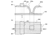
ここでは、半導体装置の一例を示す。図1(A)に上面図を示す。また、図1(B)は、図1(A)中の点線A−A’で切断した断面図に対応する図である。
(Embodiment 1)
Here, an example of a semiconductor device is shown. A top view is shown in FIG. FIG. 1B is a diagram corresponding to a cross-sectional view taken along a dotted line AA ′ in FIG.
図1(A)では、3個の記憶素子を示している。ここでは3個の記憶素子の例を示したが、説明を簡単にするためであり、個数は特に限定されず、半導体装置の設計者が所望のビット数に合わせて設ければよい。例えば、8ビット、16ビット、32ビット、64ビットなどに合わせて記憶素子を形成すればよい。図1(B)に示すように記憶素子は、絶縁表面を有する基板101上に第1の導電層102と、第2の導電層103と、それらの間に配置された混合膜104とを含む構成となっている。
In FIG. 1A, three memory elements are shown. Although an example of three memory elements is shown here, the number is not particularly limited, and the number is not particularly limited, and a semiconductor device designer may be provided in accordance with a desired number of bits. For example, a memory element may be formed in accordance with 8 bits, 16 bits, 32 bits, 64 bits, or the like. As shown in FIG. 1B, the memory element includes a first
混合膜104は、幅が電極間隔dよりも広く、第1の導電層102及び第2の導電層103上に一部重なっている。また、混合膜104は、図1(A)の上面形状に限定されず、少なくとも第1の導電層102の側面と、該側面に対向する第2の導電層103の側面との間に配置する。
The
また、混合膜104は、3つの記憶素子に延在させた一つのパターン形状となっているが、隣り合う記憶素子の間隔が電極間隔dよりも広くすることが好ましい。また、混合膜104は、3つの記憶素子に延在させているが、それぞれ記憶素子毎に独立に設けてもよい。
In addition, the
混合膜は、無機化合物と有機化合物及びハロゲン原子を含む。混合膜に用いる無機化合物としては、無機酸化物が挙げられる。具体的には、遷移金属酸化物を挙げることができる。また、元素周期表における第4族乃至第8族に属する金属の酸化物を挙げることができる。具体的には、酸化バナジウム、酸化ニオブ、酸化タンタル、酸化クロム、酸化モリブデン、酸化タングステン、酸化マンガン、酸化レニウムは電子受容性が高いため好ましい。この他、酸化インジウムや酸化亜鉛、酸化錫を用いることもできる。中でも特に、酸化モリブデンは大気中でも安定であり、吸湿性が低く、扱いやすいため、蒸着法を用いて混合膜を形成する場合には好ましい。特に、三酸化モリブデンであることが好ましい。 The mixed film contains an inorganic compound, an organic compound, and a halogen atom. An inorganic oxide is mentioned as an inorganic compound used for a mixed film. Specific examples include transition metal oxides. In addition, oxides of metals belonging to Groups 4 to 8 in the periodic table can be given. Specifically, vanadium oxide, niobium oxide, tantalum oxide, chromium oxide, molybdenum oxide, tungsten oxide, manganese oxide, and rhenium oxide are preferable because of their high electron accepting properties. In addition, indium oxide, zinc oxide, and tin oxide can also be used. Among these, molybdenum oxide is particularly preferable in the case of forming a mixed film by an evaporation method because it is stable in the air, has a low hygroscopic property, and is easy to handle. In particular, molybdenum trioxide is preferable.
混合膜に用いる有機化合物としては、芳香族アミン化合物、カルバゾール誘導体、芳香族炭化水素、高分子化合物(オリゴマー、デンドリマー、ポリマー等)など、種々の化合物を用いることができる。なお、混合膜に用いる有機化合物としては、10−6cm2/Vs以上のホール移動度を有する物質(ホール輸送材料)であることが好ましい。但し、電子よりもホールの輸送性の高い物質であれば、これら以外のものを用いてもよい。以下では、混合膜に用いることのできる有機化合物を具体的に列挙する。 As the organic compound used for the mixed film, various compounds such as aromatic amine compounds, carbazole derivatives, aromatic hydrocarbons, and high molecular compounds (oligomers, dendrimers, polymers, and the like) can be used. Note that the organic compound used for the mixed film is preferably a substance having a hole mobility of 10 −6 cm 2 / Vs or more (hole transport material). Note that other than these substances, any substance that has a property of transporting more holes than electrons may be used. Below, the organic compound which can be used for a mixed film is enumerated concretely.
例えば、混合膜に用いることのできる芳香族アミン化合物としては、N,N’−ビス(4−メチルフェニル)(p−トリル)−N,N’−ジフェニル−p−フェニレンジアミン(略称:DTDPPA)、4,4’−ビス[N−(4−ジフェニルアミノフェニル)−N−フェニルアミノ]ビフェニル(略称:DPAB)、4,4’−ビス(N−{4−[N’−(3−メチルフェニル)−N’−フェニルアミノ]フェニル}−N−フェニルアミノ)ビフェニル(略称:DNTPD)、1,3,5−トリス[N−(4−ジフェニルアミノフェニル)−N−フェニルアミノ]ベンゼン(略称:DPA3B)等を挙げることができる。 For example, as an aromatic amine compound that can be used for a mixed film, N, N′-bis (4-methylphenyl) (p-tolyl) -N, N′-diphenyl-p-phenylenediamine (abbreviation: DTDPPA) 4,4′-bis [N- (4-diphenylaminophenyl) -N-phenylamino] biphenyl (abbreviation: DPAB), 4,4′-bis (N- {4- [N ′-(3-methyl Phenyl) -N′-phenylamino] phenyl} -N-phenylamino) biphenyl (abbreviation: DNTPD), 1,3,5-tris [N- (4-diphenylaminophenyl) -N-phenylamino] benzene (abbreviation) : DPA3B) and the like.
混合膜に用いることのできるカルバゾール誘導体としては、具体的には、3−[N−(9−フェニルカルバゾール−3−イル)−N−フェニルアミノ]−9−フェニルカルバゾール(略称:PCzPCA1)、3,6−ビス[N−(9−フェニルカルバゾール−3−イル)−N−フェニルアミノ]−9−フェニルカルバゾール(略称:PCzPCA2)、3−[N−(1−ナフチル)−N−(9−フェニルカルバゾール−3−イル)アミノ]−9−フェニルカルバゾール(略称:PCzPCN1)等を挙げることができる。 Specific examples of the carbazole derivative which can be used for the mixed film include 3- [N- (9-phenylcarbazol-3-yl) -N-phenylamino] -9-phenylcarbazole (abbreviation: PCzPCA1), 3 , 6-Bis [N- (9-phenylcarbazol-3-yl) -N-phenylamino] -9-phenylcarbazole (abbreviation: PCzPCA2), 3- [N- (1-naphthyl) -N- (9- Phenylcarbazol-3-yl) amino] -9-phenylcarbazole (abbreviation: PCzPCN1) and the like.
また、混合膜に用いることのできるカルバゾール誘導体としては、4,4’−ジ(N−カルバゾリル)ビフェニル(略称:CBP)、1,3,5−トリス[4−(N−カルバゾリル)フェニル]ベンゼン(略称:TCPB)、9−[4−(10−フェニル−9−アントリル)フェニル]−9H−カルバゾール(略称:CzPA)、1,4−ビス[4−(N−カルバゾリル)フェニル]−2,3,5,6−テトラフェニルベンゼン等を用いることができる。 As the carbazole derivative that can be used for the mixed film, 4,4′-di (N-carbazolyl) biphenyl (abbreviation: CBP), 1,3,5-tris [4- (N-carbazolyl) phenyl] benzene (Abbreviation: TCPB), 9- [4- (10-phenyl-9-anthryl) phenyl] -9H-carbazole (abbreviation: CzPA), 1,4-bis [4- (N-carbazolyl) phenyl] -2, 3,5,6-tetraphenylbenzene or the like can be used.
また、混合膜に用いることのできる芳香族炭化水素としては、例えば、2−tert−ブチル−9,10−ジ(2−ナフチル)アントラセン(略称:t−BuDNA)、2−tert−ブチル−9,10−ジ(1−ナフチル)アントラセン、9,10−ビス(3,5−ジフェニルフェニル)アントラセン(略称:DPPA)、2−tert−ブチル−9,10−ビス(4−フェニルフェニル)アントラセン(略称:t−BuDBA)、9,10−ジ(2−ナフチル)アントラセン(略称:DNA)、9,10−ジフェニルアントラセン(略称:DPAnth)、2−tert−ブチルアントラセン(略称:t−BuAnth)、9,10−ビス(4−メチル−1−ナフチル)アントラセン(略称:DMNA)、9,10−ビス[2−(1−ナフチル)フェニル]−2−tert−ブチルアントラセン、9,10−ビス[2−(1−ナフチル)フェニル]アントラセン、2,3,6,7−テトラメチル−9,10−ジ(1−ナフチル)アントラセン、2,3,6,7−テトラメチル−9,10−ジ(2−ナフチル)アントラセン、9,9’−ビアントリル、10,10’−ジフェニル−9,9’−ビアントリル、10,10’−ビス(2−フェニルフェニル)−9,9’−ビアントリル、10,10’−ビス[(2,3,4,5,6−ペンタフェニル)フェニル]−9,9’−ビアントリル、アントラセン、テトラセン、ルブレン、ペリレン、2,5,8,11−テトラ(tert−ブチル)ペリレン等が挙げられる。また、この他、ペンタセン、コロネン等も用いることができる。このように、1×10−6cm2/Vs以上の移動度を有し、炭素数14〜42である芳香族炭化水素を用いることがより好ましい。 Examples of aromatic hydrocarbons that can be used for the mixed film include 2-tert-butyl-9,10-di (2-naphthyl) anthracene (abbreviation: t-BuDNA), 2-tert-butyl-9. , 10-di (1-naphthyl) anthracene, 9,10-bis (3,5-diphenylphenyl) anthracene (abbreviation: DPPA), 2-tert-butyl-9,10-bis (4-phenylphenyl) anthracene ( Abbreviations: t-BuDBA), 9,10-di (2-naphthyl) anthracene (abbreviation: DNA), 9,10-diphenylanthracene (abbreviation: DPAnth), 2-tert-butylanthracene (abbreviation: t-BuAnth), 9,10-bis (4-methyl-1-naphthyl) anthracene (abbreviation: DMNA), 9,10-bis [2- (1-na Til) phenyl] -2-tert-butylanthracene, 9,10-bis [2- (1-naphthyl) phenyl] anthracene, 2,3,6,7-tetramethyl-9,10-di (1-naphthyl) Anthracene, 2,3,6,7-tetramethyl-9,10-di (2-naphthyl) anthracene, 9,9′-bianthryl, 10,10′-diphenyl-9,9′-bianthryl, 10,10 ′ -Bis (2-phenylphenyl) -9,9'-bianthryl, 10,10'-bis [(2,3,4,5,6-pentaphenyl) phenyl] -9,9'-bianthryl, anthracene, tetracene , Rubrene, perylene, 2,5,8,11-tetra (tert-butyl) perylene, and the like. In addition, pentacene, coronene, and the like can also be used. Thus, it is more preferable to use an aromatic hydrocarbon having a mobility of 1 × 10 −6 cm 2 / Vs or more and having 14 to 42 carbon atoms.
なお、混合膜に用いることのできる芳香族炭化水素は、ビニル骨格を有していてもよい。ビニル基を有している芳香族炭化水素としては、例えば、4,4’−ビス(2,2−ジフェニルビニル)ビフェニル(略称:DPVBi)、9,10−ビス[4−(2,2−ジフェニルビニル)フェニル]アントラセン(略称:DPVPA)等が挙げられる。 Note that the aromatic hydrocarbon that can be used for the mixed film may have a vinyl skeleton. As the aromatic hydrocarbon having a vinyl group, for example, 4,4′-bis (2,2-diphenylvinyl) biphenyl (abbreviation: DPVBi), 9,10-bis [4- (2,2- Diphenylvinyl) phenyl] anthracene (abbreviation: DPVPA) and the like.
混合膜に用いるハロゲン原子としては、フッ素や塩素が適している。但し、ここに示したものに限らず、その他の物質を用いてもよい。 Fluorine or chlorine is suitable as the halogen atom used for the mixed film. However, it is not limited to those shown here, and other substances may be used.
第1の導電層102及び第2の導電層103の材料としては、Ta、W、Ti、Mo、Al、Cu、Ag、Au、In、Znから選ばれた元素、または前記元素を主成分とする合金材料若しくは化合物材料の単層、またはこれらの積層で形成してもよい。また、リン等の不純物元素をドーピングした多結晶シリコン膜に代表される半導体膜を用いてもよい。
As a material of the first
また、第1の導電層102及び第2の導電層103は異なる材料を用いて別々の工程で形成してもよい。製造工程数を低減する上では、第1の導電層102及び第2の導電層103は同じ材料を用いることが好ましい。また、第1の導電層102及び第2の導電層103を同じ材料とすると、位置合わせを高精度に行うこともできる。
Alternatively, the first
また、第1の導電層102及び第2の導電層103は電圧が印加され、発熱するため、表面が露呈していると酸化して配線抵抗が高くなってしまう恐れがある。従って、第1の導電層102及び第2の導電層103を覆う保護膜を設けることが好ましい。また、第1の導電層102及び第2の導電層103の材料として、酸化してもある程度の導電性を有する材料、例えばTiやZnなどを用いる場合には特に保護膜を設けなくてもよい。
Further, since voltage is applied to the first
また、図1(A)において、第1の導電層102及び第2の導電層103の上面形状は、矩形状としているが、特に限定されず、折れ曲がった形状や、鋭角な突出部を有する形状であってもよい。また、一つの記憶素子において、第1の導電層102と第2の導電層103の間隔が一定でなくともよく、一方または両方の上面形状を、互いの間隔が部分的に狭くなるような形状であってもよい。この場合、電極間隔dは最も狭い間隔距離を指す。部分的に間隔を狭くした部分には電界が集中するため、より低い書き込み電圧値で記憶素子へ書き込みを行うことができる。
In FIG. 1A, the top shape of the first
図1(A)及び図1(B)に示す記憶素子は、電極間隔dで設けられた一対の電極に電圧を印加することで、混合膜が基板から剥がれることによって一対の電極間の抵抗値を大幅に増加させることで記憶素子の書き込みを行うことができる。また、記憶素子に電圧印加を行わなければ、混合膜が一対の電極間に存在しており、導電率を高く保持することができる。このように、電圧印加の有無で記憶素子の電気抵抗値を大幅に変化させることで、記憶素子に2値を記憶させることができる。 In the memory element illustrated in FIGS. 1A and 1B, the resistance value between a pair of electrodes is applied by applying a voltage to a pair of electrodes provided at an electrode interval d so that the mixed film is peeled off from the substrate. The memory element can be written by significantly increasing. If no voltage is applied to the memory element, the mixed film exists between the pair of electrodes, and the conductivity can be kept high. In this manner, binary values can be stored in the storage element by significantly changing the electrical resistance value of the storage element with or without voltage application.
また、一旦、一対の電極間に電圧をかけて記憶素子への書き込みを行った記憶素子は、電圧印加前の電気抵抗値に戻ることはない。不揮発性を有している。 In addition, the memory element that has once written to the memory element by applying a voltage between the pair of electrodes does not return to the electric resistance value before voltage application. It has non-volatility.
(実施の形態2)
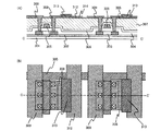
ここでは、ビット線とワード線とを交差させ、交差させた近傍に記憶素子を設けるパッシブマトリクス型の記憶素子を含む記憶装置の例を示す。図2(B)に上面図を示す。また、図2(A)は、図2(B)中の点線B−B’で切断した断面図に対応する図である。
(Embodiment 2)
Here, an example of a memory device including a passive matrix memory element in which a bit line and a word line are crossed and a memory element is provided in the vicinity of the crossing is shown. A top view is shown in FIG. FIG. 2A is a diagram corresponding to a cross-sectional view taken along a dotted line BB ′ in FIG.
図2(A)において、絶縁表面を有する基板上にワード線202が設けられ、ワード線202上には第1の絶縁層203a、203bが設けられている。第1の絶縁層203a、第1の絶縁層203bは、基板面に対して垂直な膜厚0.8μmから1.5μmとする。絶縁表面を有する基板は、ガラス基板や、石英基板や、プラスチック基板を用いる。他に用いることのできる基板として、半導体基板、SOI基板、セラミックス基板、または表面に絶縁膜を形成した金属基板なども用いることができる。
In FIG. 2A, a
第1の絶縁層203a、第1の絶縁層203bは同じ材料で形成されており、ワード線202に達する開口(コンタクトホール)が設けられている。この開口を覆うようにワード線電極204が設けられている。また、開口を介してワード線202と電気的に接続しているワード線電極204は、第1の絶縁層203a、203b上に設ける。図2(A)では、同じ平面上に、即ち第1の絶縁層203a上にワード線電極204とビット線201とを設けている。
The first insulating
ワード線202は、メモリセルアレイの中から一列を選択するための制御信号線である。メモリセルアレイは、マトリクス状に複数のメモリセルが配置されたものである。一つの記憶素子は、ワード線202とビット線201の交点付近にそれぞれ一つ配置されており、読み出し、書き込みを行なうアドレスに対応するワード線の電圧を印加することで書き込み、読み出しが可能になる。
The
また、ビット線201は、メモリセルアレイからデータを取り出すための信号線である。電圧が印加されたワード線202に接続されているメモリセルが、記憶素子に記録されたデータをビット線201に出力することで、データの読み出しが行われる。
The
また、ワード線電極204とビット線201との間に混合膜205を設ける。混合膜205は、ワード線202とビット線201の交点付近に配置された一つ一つの記憶素子に独立して形成している。
Further, a
また、ワード線電極204とビット線201の側面をテーパー形状としている。電極間隔dは、対向する側面の下端部の距離となる。
Further, the side surfaces of the
図2(A)に示すように、混合膜205は、ワード線電極204の一方側の側面(テーパー状の側面)に接している。また、混合膜205に接しているワード線電極204の側面に対向するビット線201の側面も混合膜205に接している。
As shown in FIG. 2A, the
また、工程数削減のため、同一工程でワード線電極204とビット線201とを形成することが好ましい。また、ワード線電極204とビット線201との間隔dを精密に制御するため、同じフォトマスクを用いて、ワード線電極204とビット線201とをパターニングすることが好ましい。ワード線電極204とビット線201との距離間隔dを狭めることによって低電圧での書き込みを行うことができる。すなわち、低消費電力で書き込みを行うことが可能となる。
In order to reduce the number of processes, it is preferable to form the
ワード線202やビット線201やワード線電極204は、蒸着法、スパッタ法、CVD法、印刷法、電解メッキ法、無電解メッキ法、または液滴吐出法等を用いて形成する。
The
混合膜205には有機化合物を含んでいるため、混合膜よりも先にビット線201及びワード線電極204を形成することはプロセス上有用である。混合膜205よりも先にビット線201及びワード線電極204を形成するため、用いる配線の形成方法、特に成膜温度が限定されず、様々な方法を用いることができる点が長所である。
Since the
また、ワード線202とビット線201とワード線電極204は、互いに異なる材料を使用してもよい。また、ワード線202とビット線201とワード線電極204は、配線の形成方法も互いに異なるものとしてもよい。
Further, different materials may be used for the
また、パターニング時のエッチング条件を適宜調節することにより、テーパー状の側面を有するビット線201及びワード線電極204を形成することができる。同一工程で形成する場合にはビット線201及びワード線電極204は同じテーパー形状となる。テーパー形状とは、電極の側面の断面が傾斜していることである。好ましくは、基板面に対してビット線201及びワード線電極204の側面は、10度以上85度未満、好ましくは60度以上80度以下の傾斜角度を有する。
Further, the
図2(A)では、ビット線201は、ワード線202上方に設けた例を示しているが、特に形成順序は限定されず、ビット線上方にワード線を配置してもよい。ビット線上方にワード線を配置する場合、第1の絶縁層の開口を介してビット線と電気的に接続するビット線電極を設け、ビット線電極とワード線との間に混合膜を配置する構成となる。
2A shows an example in which the
このように、ビット線とワード線とを交差させ、交差させた近傍に記憶素子を設けるパッシブマトリクス型の記憶素子とすることによって、記憶素子の占有面積の縮小化が図れる。 In this manner, by occupying the bit line and the word line and forming the passive matrix storage element in which the storage element is provided in the vicinity of the intersection, the area occupied by the storage element can be reduced.
また、本実施の形態は実施の形態1と自由に組み合わせることができる。
Further, this embodiment mode can be freely combined with
(実施の形態3)
ここでは、アクティブマトリクス型の記憶装置の一例を示す。図3(B)に上面図を示す。また、図3(A)は、図3(B)中の点線C−C’で切断した断面図に対応する図である。
(Embodiment 3)
Here, an example of an active matrix storage device is shown. FIG. 3B shows a top view. FIG. 3A is a diagram corresponding to a cross-sectional view taken along a dotted line CC ′ in FIG.
図3(A)において、絶縁表面を有する基板301上に第1の絶縁層302が設けられ、第1の絶縁層302上には半導体層303が設けられている。第1の絶縁層302、半導体層303上には第2の絶縁層304が設けられ、第2の絶縁層304上にはワード線(ゲート線)305が設けられている。ワード線(ゲート線)305上には第3の絶縁層306が設けられ、第3の絶縁層306上には第4の絶縁層307が設けられている。第4の絶縁層307上にはビット線309、第1の電極308及び、コモン電極312が設けられている。ビット線309、第1の電極308及び、コモン電極312は同じ材料で形成されている。第2の絶縁層304、第3の絶縁層306及び、第4の絶縁層307には半導体層303に達する左右一対の開口(コンタクトホール)が合計6個設けられている。この開口を覆うようにビット線309、及び第1の電極308が設けられている。同じ層に、即ち第4の絶縁層307上にビット線309と第1の電極308とコモン電極312とを設けている。
In FIG. 3A, a first insulating
半導体層303、ワード線(ゲート線)305、第1の電極308、及びビット線309はトランジスタを構成している。
The
図3(A)においては、混合膜313が第1の電極308、及びコモン電極312の側面、及び上面の一部(上端部)と接している。混合膜313の幅は少なくとも電極間隔Dxよりも大きい。
In FIG. 3A, the
また、図3(A)に示す記憶素子において、ビット線309、第1の電極308、コモン電極312、及び混合膜313を覆うように保護層314を設けてもよい。
3A, a
本実施の形態では、アクティブマトリクス型の記憶装置とすることで、記憶素子の集積化を図ることができる。また、電極間隔Dxを狭くすることで低消費電力化を図ることができる。 In this embodiment mode, an active matrix memory device can be used to integrate the memory elements. Further, the power consumption can be reduced by narrowing the electrode interval Dx.
また、本実施の形態は実施の形態1または実施の形態2と自由に組み合わせることができる。
Further, this embodiment mode can be freely combined with
本実施例では、実施の形態2で示したパッシブマトリクス型の記憶装置の構成とデータの書き込み方法について説明する。
In this example, a structure and a data writing method of the passive matrix memory device described in
図4(A)においてワード線はWn(1≦n≦y)、ビット線はBm(1≦m≦x)である。 In FIG. 4A, the word line is Wn (1 ≦ n ≦ y), and the bit line is Bm (1 ≦ m ≦ x).
図4(A)に本発明の記憶装置の構成を示す。本発明の記憶装置5008はカラムデコーダ5001、ローデコーダ5002、読み出し回路5004、書き込み回路5005、セレクタ5003、メモリセルアレイ22を有する。メモリセルアレイ22は複数のメモリセル21を有する。
FIG. 4A shows the structure of the memory device of the present invention. A
メモリセル21は、一つの記憶素子80を有する。
The
本発明においては、実施の形態2に示したように、ビット線(第1の導電層)と、ワード線に接続されたワード線電極(第2の導電層)とが同一平面上に形成されている。記憶素子80は、ワード線電極と、ビット線と、ワード線電極とビット線との間に混合膜とを有する。
In the present invention, as shown in the second embodiment, the bit line (first conductive layer) and the word line electrode (second conductive layer) connected to the word line are formed on the same plane. ing. The
なお、ここで示す記憶装置5008の構成はあくまで一例であり、読み出し方式や書き込み方式によって適切な回路構成とすればよい。
Note that the structure of the
カラムデコーダ5001はメモリセルアレイの列を指定するアドレス信号を受けて、セレクタ5003に信号を与える。セレクタ5003はカラムデコーダ5001の信号を受けて指定列のビット線を選択し、選択されたビット線を書き込み回路5005や読み出し回路5004に接続する。ローデコーダ5002はメモリセルアレイの行を指定するアドレス信号を受けて、指定行のワード線に所定の電位を与える。上記動作によりアドレス信号に対応する一つのメモリセル21が選択される。読み出し回路5004は選択されたメモリセルが有するデータを読み出し、増幅して出力する。書き込み回路5005は書き込みに必要な電圧を生成し、選択されたメモリセルの記憶素子に電圧を印加することでデータの書き込みを行う。
The
図4(B)に本発明の記憶装置が有する書き込み回路5005の構成を示す。書き込み回路5005は電圧発生回路7001、タイミング制御回路7002、スイッチSW0、SW1、出力端子Pwを有する。また、書き込み制御信号(WEと記載する)、データ信号(DATAと記載する)、クロック信号(CLKと記載する)等が入力される。電圧発生回路7001は昇圧回路等で構成され、書き込みに必要な電圧V1を生成し、出力端子Paから出力する。タイミング制御回路7002は、スイッチSW0、SW1をそれぞれ制御する信号S0、S1を生成し、それぞれ出力端子P0、P1から出力する。スイッチSW0は接地電位との接続、SW1は電圧発生回路7001の出力端子Paとの接続を制御し、これらのスイッチによって、書き込み回路の出力端子Pwからの出力電圧Vwを切り替えることができる。
FIG. 4B illustrates a structure of the
次に記憶素子の導電性を変化させない初期状態を「0」とし、記憶素子の導電性を変化させる電極間抵抗が高い場合を「1」としたときの書き込み動作について説明する。まず入力信号WEがHighレベルになると、列を指定するアドレス信号を受けたカラムデコーダ5001はセレクタ5003に信号を与え、セレクタ5003は指定列のビット線を書き込み回路の出力端子Pwに接続する。指定されていないビット線は非接続(フローティングと記載する)状態となる。同様に行を指定するアドレス信号を受けたローデコーダ5002は指定行のワード線に電圧V2を印加し、指定されていないワード線はフローティングとなる。上記動作によりアドレス信号に対応する一つの記憶素子80が選択される。
Next, the writing operation when the initial state in which the conductivity of the memory element is not changed is set to “0” and the case where the interelectrode resistance for changing the conductivity of the memory element is high is set to “1” will be described. First, when the input signal WE becomes High level, the
同時に入力信号DATAがHighレベルを受けることにより、タイミング制御回路7002は信号S0=Lowレベル、S1=Highレベルを生成し、出力端子P0、P1から出力する。当該信号によりスイッチSW0がオフ、SW1オンになり、書き込み回路5005は出力端子Pwから出力電圧Vwとして電圧V1を出力する。
At the same time, when the input signal DATA receives the high level, the
選択された記憶素子は、上記動作により第1の導電層に電圧V1が印加され、第2の導電層に電圧V2が印加される。すると混合膜が剥がれる。その結果、記憶素子の導電性が変化し、高抵抗状態になり「1」が書き込まれる。電圧V1、V2は記憶装置に電圧V1−V2を印加することにより記憶装置の導電性が変化する範囲から決定する。 In the selected memory element, the voltage V1 is applied to the first conductive layer and the voltage V2 is applied to the second conductive layer by the above operation. Then, the mixed film is peeled off. As a result, the conductivity of the memory element is changed to be in a high resistance state, and “1” is written. The voltages V1 and V2 are determined from a range in which the conductivity of the memory device is changed by applying the voltage V1-V2 to the memory device.
また入力信号WEがLowレベルになると、全てのビット線とワード線がフローティング状態となる。上記動作により、書き込みは行われなくなる。 When the input signal WE becomes low level, all the bit lines and word lines are in a floating state. With the above operation, writing is not performed.
次に、「0」の書き込みを説明する。「0」の書き込みは記憶素子の導電性を変化させない書き込みであり、これは記憶素子に電圧を印加しない。つまり初期状態を維持することで実現される。まず「1」の書き込みと同様に入力信号WEがHighレベル(書き込み許可となる高い電圧)になると、列を指定するアドレス信号を受けたカラムデコーダ5001は指定列のセレクタ5003に信号を与え、セレクタ5003は指定列のビット線を書き込み回路の出力端子Pwに接続する。このとき指定されていないビット線はフローティング状態となる。同様に行を指定するアドレス信号を受けたローデコーダ5002は指定行のワード線にV2を印加し、指定されていないワード線はフローティング状態となる。上記動作によりアドレス信号に対応する一つの記憶素子80が選択される。
Next, writing of “0” will be described. Writing “0” is writing that does not change the conductivity of the memory element, and does not apply a voltage to the memory element. That is, it is realized by maintaining the initial state. First, as in the case of writing “1”, when the input signal WE is at a high level (a high voltage at which writing is permitted), the
同時に入力信号DATAがLowレベルを受け、タイミング制御回路7002はそれぞれ制御信号S0=Highレベル、S1=Lowレベルを生成し、当該制御信号を出力端子P0、P1からそれぞれ出力する。当該制御信号によりスイッチSW0はオン、SW1はオフとなり、出力端子Pwから出力電圧Vwとして0Vを出力する。
At the same time, the input signal DATA receives the Low level, the
選択された記憶素子は、上記動作によりビット線に0Vが印加され、ワード線にV2が印加される。電圧V2は記憶装置に電圧V2を印加することにより記憶装置の導電性が変化しない範囲から決定する。記憶素子の導電性は変化しないので、初期状態である「0」を維持する。 In the selected memory element, 0V is applied to the bit line and V2 is applied to the word line by the above operation. The voltage V2 is determined from a range in which the conductivity of the memory device does not change by applying the voltage V2 to the memory device. Since the conductivity of the memory element does not change, the initial state “0” is maintained.
入力信号WEがLowレベルになると、全てのビット線とワード線はフローティング状態となる。 When the input signal WE becomes low level, all the bit lines and word lines are in a floating state.
このようにして「1」又は「0」の書き込みを行うことができる。 In this way, “1” or “0” can be written.
次に、データ読み出しについて説明する。 Next, data reading will be described.
図5においてワード線は14である。またビット線は16である。 In FIG. 5, there are 14 word lines. The number of bit lines is 16.
書き込み時と同様にアドレス信号に対応する一つの記憶素子18aが選択される。図5には一つの選択されたセル18aと、他の非選択セル18bが示されている。選択セル18aに接続されたワード線14は電圧Vsが印加され、他の指定されていないワード線はフローティング状態となる。また、選択セル18aに接続されたビット線には読み出し回路が接続され、指定されていないビット線はフローティング状態となる。読み出し回路では、選択セル18aに流れる電流から、メモリの状態が1であるか0であるかを判別する。
Similar to the writing, one
また、本実施例は、実施の形態1、実施の形態2、または実施の形態3と自由に組み合わせることができる。
Further, this embodiment can be freely combined with
本実施例では、図6(A)及び図6(B)に示す等価回路を用いて、実施の形態3で示したアクティブマトリクス型の記憶装置の構成とデータの書き込み方法について説明する。
In this example, the structure of the active matrix memory device described in
本実施例で示す記憶装置の一構成例は、カラムデコーダ801、ローデコーダ802、読み出し回路804、書き込み回路805、セレクタ803、メモリセルアレイ822を有する。メモリセルアレイ822はビット線Bm(1≦m≦x)、ワード線Wn(1≦n≦y)、ビット線とワード線との交点にx×y個のメモリセル821を有する。
One structural example of the memory device shown in this embodiment includes a
メモリセル821は、ビット線Bx(1≦x≦m)を構成する第1の配線と、ワード線Wy(1≦y≦n)を構成する第2の配線と、トランジスタ840と、記憶素子841とを有する。記憶素子841は、実施の形態3のように、平行に並べて配置された一対の導電層の間に、混合膜が挟まれた構造を有する。
The
なお、ここで示す記憶装置816の構成はあくまで一例であり、読み出し方式や書込み方式によって適切な回路構成とすればよい。
Note that the structure of the
カラムデコーダ801はメモリセルアレイの列を指定するアドレス信号を受けて、セレクタ803に信号を与える。セレクタ803はカラムデコーダ801の信号を受けて指定列のビット線を選択する。ローデコーダ802はメモリセルアレイの行を指定するアドレス信号を受けて、指定行のワード線を選択する。上記動作によりアドレス信号に対応する一つのメモリセル821が選択される。
The
メモリセル821はトランジスタ840と記憶素子841とを有する。本明細書の添付図においてメモリセル821は長方形を用いて表す。トランジスタ840はゲート電極にワード線が接続され、トランジスタの一方の高濃度不純物領域にビット線が接続され、トランジスタのもう一方の高濃度不純物領域に記憶素子841の第1の電極が接続されている。記憶素子の第2の電極はメモリセルアレイ内の全ての記憶素子の第2の電極と導通しており、記憶装置の動作時、つまり書き込み時、読み出し時に共通の電圧が印加される。読み出し回路804は選択されたメモリセルの記憶素子の状態を判別することで、メモリセルに格納されたデータを読み出して出力する。書き込み回路805は書き込みに必要な電圧を生成し、選択されたメモリセルの記憶素子に電圧を印加することでデータの書き込みを行う。
The
図6(B)に本発明の記憶装置が有する書き込み回路805の構成を示す。書き込み回路805は電圧発生回路811、タイミング制御回路812、スイッチSW0、SW1、出力端子Pwを有する。また、書き込み制御信号(WEと記載する)、データ信号(DATAと記載する)、クロック信号(CLKと記載する)等が入力される。電圧発生回路811は昇圧回路等で構成され、書き込みに必要な電圧V1を生成し、出力端子Paから出力する。タイミング制御回路812は、スイッチSW0、SW1をそれぞれ制御する信号S0、S1を生成し、それぞれ出力端子P0、P1から出力する。スイッチSW0は接地との接続、スイッチSW1は電圧発生回路811の出力Paとの接続を制御し、スイッチがいずれかの接続状態となるかによって、書き込み回路の出力端子Pwからの出力電圧Vwを切り替えることができる。
FIG. 6B illustrates a structure of the
次に記憶素子の導電性を変化させない初期状態を「0」とし、記憶素子の導電性を変化させ高抵抗の場合を「1」としたときの書き込み動作について説明する。まず入力信号WEがHighレベルになると、列を指定するアドレス信号を受けたカラムデコーダ801はセレクタ803に信号を与え、セレクタ803は指定列のビット線と書き込み回路の出力端子Pwとを電気的に接続する。指定されていないビット線は非接続(フローティングと記載する)状態となっている。指定行のビット線には書き込み回路の出力電圧Vwが印加される。同様に行を指定するアドレス信号を受けたローデコーダ802は指定行のワード線に電圧V2を印加し、指定されていないワード線に0Vを印加する。上記動作によりアドレス信号に対応する一つの記憶素子841が選択される。電圧V2はゲート電極に電圧V2を印加するとトランジスタ840がオン状態になる範囲から決定する。
Next, the writing operation when the initial state in which the conductivity of the memory element is not changed is set to “0” and the conductivity of the memory element is changed to be “1” when the resistance is high will be described. First, when the input signal WE becomes High level, the
同時にHighレベルのデータ信号DATAを受けることにより、電圧発生回路811は電圧V1を生成し、出力Paから出力することができる。タイミング制御回路812は入力信号WE、DATA、CLK、電源電位(VDD)等から、スイッチSW0、SW1を制御する信号S0=Lowレベル、S1=Highレベルを生成し、出力P0、P1から出力することができる。当該信号S0、S1によりスイッチSW0はオフ、SW1はオンとなり、書き込み回路805は出力端子Pwから出力電圧Vwとして電圧V1を出力することができる。
At the same time, by receiving the high level data signal DATA, the
選択された記憶素子は、上記動作によりワード線に電圧V2が印加され、ビット線に電圧V1が印加され、第2の電極には0Vが印加されているので、記録素子には電圧V1が印加される。すると薄膜トランジスタの不純物領域が導通して、ビット線の電圧V1が記憶素子に印加される。その結果、記憶素子の導電性が変化し、高抵抗状態となり「1」が書き込まれる。 In the selected memory element, the voltage V2 is applied to the word line, the voltage V1 is applied to the bit line, and 0 V is applied to the second electrode by the above operation, so the voltage V1 is applied to the recording element. Is done. Then, the impurity region of the thin film transistor is turned on, and the voltage V1 of the bit line is applied to the memory element. As a result, the conductivity of the memory element is changed to be in a high resistance state, and “1” is written.
また入力信号WEがLowレベルになると、全てのワード線は0Vとなり、全てのビット線はフローティング状態となる。同時にタイミング制御回路812は信号S0、S1としてそれぞれLowレベルを生成し、出力端子P0、P1から出力し、出力端子Pwはフローティング状態となる。上記動作により、「1」の書き込みは終了する。
When the input signal WE becomes low level, all the word lines are set to 0V and all the bit lines are in a floating state. At the same time, the
次に、「0」の書き込みを説明する。「0」の書き込みは記憶素子の導電性を変化させない書き込みであり、これは記憶素子に電圧を印加しない、つまり初期状態を維持することで実現される。まず「1」の書き込みと同様に入力信号WEがHighレベルになると、列を指定するアドレス信号を受けたカラムデコーダ801は指定列のセレクタに信号を与え、セレクタ803は指定列のビット線を書き込み回路の出力端子Pwに接続する。このとき指定されていないビット線はフローティング状態となる。同様に行を指定するアドレス信号を受けたローデコーダ802は指定行のワード線に電圧V2を印加し、指定されていないワード線に0Vを印加する。上記動作によりアドレス信号に対応する一つの記憶素子841が選択される。
Next, writing of “0” will be described. Writing “0” is writing that does not change the conductivity of the memory element, and this is realized by applying no voltage to the memory element, that is, maintaining the initial state. First, when the input signal WE becomes high level as in the case of writing “1”, the
同時にLowレベルの入力信号DATAを受け、タイミング制御回路812はそれぞれ制御信号S0=Highレベル、S1=Lowレベルを生成し、当該制御信号を出力P0、P1からそれぞれ出力する。当該制御信号によりスイッチSW0はオン、SW1はオフとなり、出力端子Pwから出力電圧Vwとして0Vを出力する。
At the same time, upon receiving the low level input signal DATA, the
選択された記憶素子は、上記動作によりワード線にV2が印加され、トランジスタがオン状態になるがビット線に繋がっている第1の電極と第2の電極には0Vが印加されているため、記憶素子には電圧が印加されず、導電性は変化しないので、初期状態である「0」を維持する。 In the selected memory element, V2 is applied to the word line by the above operation, and the transistor is turned on, but 0 V is applied to the first electrode and the second electrode connected to the bit line. Since no voltage is applied to the memory element and the conductivity does not change, the initial state “0” is maintained.
入力信号WEがLowレベルになると、全てのワード線は0V、全てのビット線はフローティング状態となる。同時にタイミング制御回路812は信号S0、S1はLowレベルを生成して、それぞれ出力P0、P1から出力し、出力端子Pwはフローティング状態となる。上記動作により、「0」の書き込みは終了する。
When the input signal WE becomes low level, all the word lines are set to 0V and all the bit lines are in a floating state. At the same time, the
このようにして「1」又は「0」の書き込みを行うことができる。 In this way, “1” or “0” can be written.
また、メモリセルアレイ822は、絶縁表面を有する基板上にスイッチング素子として機能するトランジスタ840および当該トランジスタ840に接続された記憶素子841とを複数有している。
In addition, the
また、本実施例は、実施の形態2、実施の形態3、または実施の形態4と自由に組み合わせることができる。
Further, this embodiment can be freely combined with
半導体装置の構成について、図7を参照して説明する。図7に示すように、本発明の半導体装置1520は、非接触でデータを交信する機能を有し、電源回路1511、クロック発生回路1512、データ復調/変調回路1513、他の回路を制御する制御回路1514、インターフェイス回路1515、記憶回路1516、データバス1517、アンテナ(アンテナコイル)1518、センサ1523a、センサ回路1523bを有する。
A structure of the semiconductor device will be described with reference to FIG. As shown in FIG. 7, the
電源回路1511は、アンテナ1518から入力された交流信号を基に、半導体装置1520の内部の各回路に供給する各種電源を生成する回路である。クロック発生回路1512は、アンテナ1518から入力された交流信号を基に、半導体装置1520の内部の各回路に供給する各種クロック信号を生成する回路である。データ復調/変調回路1513は、リーダライタ1519と交信するデータを復調/変調する機能を有する。制御回路1514は、記憶回路1516を制御する機能を有する。アンテナ1518は、電波の送受信を行う機能を有する。リーダライタ1519は、半導体装置との交信、制御及びそのデータに関する処理を制御する。なお、半導体装置は上記構成に制約されず、例えば、電源電圧のリミッタ回路や暗号処理専用ハードウエアといった他の要素を追加した構成であってもよい。
The
記憶回路1516は、記憶素子として実施の形態1乃至3で述べた、混合膜が一対の導電層間に挟まれた記憶素子を有する。この記憶素子は、外部からの電気的作用により電気抵抗の変化が生じる。なお、記憶回路1516は、一対の導電層間に混合膜が挟まれた記憶素子のみを有していてもよいし、他の構成の記憶回路を有していてもよい。他の構成の記憶回路とは、例えば、DRAM、SRAM、FeRAM、マスクROM、PROM、EPROM、EEPROM及びフラッシュメモリから選択される1つ又は複数に相当する。
The
センサ1523aは抵抗素子、容量結合素子、誘導結合素子、光起電力素子、光電変換素子、熱起電力素子、トランジスタ、サーミスタ、ダイオードなどの半導体素子で形成される。センサ回路1523bはインピーダンス、リアクタンス、インダクタンス、電圧又は電流の変化を検出し、アナログ/デジタル変換(A/D変換)して制御回路1514に信号を出力する。
The
また、本実施例は、実施の形態1乃至3、実施例1、または実施例2と自由に組み合わせることができる。
Further, this embodiment can be freely combined with any of
本発明により無線チップとして機能する半導体装置を形成することができる。無線チップの用途は広範にわたるが、例えば、紙幣、硬貨、有価証券類、無記名債券類、証書類(運転免許証や住民票等、図9(A)参照)、包装用容器類(包装紙やボトル等、図9(C)参照)、記録媒体(DVDソフトやビデオテープ等、図9(B)参照)、乗物類(自転車等、図9(D)参照)、身の回り品(鞄や眼鏡等)、食品類、植物類、動物類、人体、衣類、生活用品類、電子機器等の商品や荷物の荷札(図9(E)、図9(F)参照)等の物品に設けて使用することができる。電子機器とは、液晶表示装置、EL表示装置、テレビジョン装置(単にテレビ、テレビ受像機、テレビジョン受像機とも呼ぶ)及び携帯電話等を指す。 According to the present invention, a semiconductor device functioning as a wireless chip can be formed. Applications of wireless chips are wide-ranging. For example, banknotes, coins, securities, bearer bonds, certificates (driver's license, resident's card, etc., see FIG. 9A), packaging containers (wrapping paper, Bottle, etc., see FIG. 9C), recording medium (DVD software, video tape, etc., see FIG. 9B), vehicles (bicycle, etc., see FIG. 9D), personal items (bags, glasses, etc.) ), Foods, plants, animals, human bodies, clothing, daily necessities, electronic equipment, etc. and goods such as luggage tags (see FIGS. 9E and 9F) and used. be able to. Electronic devices refer to liquid crystal display devices, EL display devices, television devices (also simply referred to as televisions, television receivers, television receivers), mobile phones, and the like.
本発明の半導体装置9210は、プリント基板への実装、表面への貼りつけ、または埋め込む等により、物品に固定される。例えば、本なら紙に埋め込む、または有機樹脂からなるパッケージなら当該有機樹脂に埋め込む等により、各物品に固定される。本発明の半導体装置9210は、小型、薄型、軽量を実現するため、物品に固定した後も、その物品自体のデザイン性を損なうことがない。また、紙幣、硬貨、有価証券類、無記名債券類、証書類等に本発明の半導体装置9210を設けることにより、認証機能を設けることができ、この認証機能を活用すれば、偽造を防止することができる。また、包装用容器類、記録媒体、身の回り品、食品類、衣類、生活用品類、電子機器等に本発明の半導体装置を設けることにより、検品システム等のシステムの効率化を図ることができる。
The
次に、本発明の半導体装置を実装した電子機器の一態様について図面を参照して説明する。ここで例示する電子機器は携帯電話機であり、筐体2700、2706、パネル2701、ハウジング2702、プリント配線基板2703、操作ボタン2704、バッテリ2705を有する(図8参照)。パネル2701はハウジング2702に脱着自在に組み込まれ、ハウジング2702はプリント配線基板2703に嵌着される。ハウジング2702はパネル2701が組み込まれる電子機器に合わせて、形状や寸法が適宜変更される。プリント配線基板2703には、パッケージングされた複数の半導体装置が実装されており、このうちの1つとして、本発明の半導体装置を用いることができる。プリント配線基板2703に実装される複数の半導体装置は、コントローラ、中央処理ユニット(CPU、Central Processing Unit)、メモリ、電源回路、音声処理回路、送受信回路等のいずれかの機能を有する。
Next, one mode of an electronic device in which the semiconductor device of the present invention is mounted will be described with reference to the drawings. The electronic device illustrated here is a mobile phone, which includes
パネル2701は、接続フィルム2708を介して、プリント配線基板2703と固定される。上記のパネル2701、ハウジング2702、プリント配線基板2703は、操作ボタン2704やバッテリ2705と共に、筐体2700、2706の内部に収納される。パネル2701が含む画素領域2709は、筐体2700に設けられた開口窓から視認できるように配置されている。
The
上記の通り、本発明の半導体装置は、小型、薄型、軽量であることを効果としており、上記効果により、電子機器の筐体2700、2706内部の限られた空間を有効に利用することができる。
As described above, the semiconductor device of the present invention is advantageous in that it is small, thin, and lightweight, and the above-described effects can effectively use a limited space inside the
また、本発明の半導体装置は、外部からの電気的作用により変化する混合膜が一対の導電層に挟まれた単純な構造の記憶素子を有するため、安価な半導体装置を用いた電子機器を提供することができる。また、本発明の半導体装置は高集積化が容易なため、大容量の記憶回路を有する半導体装置を用いた電子機器を提供することができる。本発明の半導体装置が有する記憶素子として、実施の形態1乃至3のいずれか一で述べた記憶素子を用いることができる。
In addition, since the semiconductor device of the present invention includes a memory element having a simple structure in which a mixed film that changes due to an external electric action is sandwiched between a pair of conductive layers, an electronic device using an inexpensive semiconductor device is provided. can do. In addition, since the semiconductor device of the present invention can be easily integrated, an electronic device using the semiconductor device including a large-capacity memory circuit can be provided. As the memory element included in the semiconductor device of the present invention, the memory element described in any one of
また、本発明の半導体装置が有する記憶装置は、外部からの電気的作用によりデータの書き込みを行うものであり、不揮発性であって、データの追記が可能である。上記特徴により、書き換えによる偽造を防止することができ、新たなデータを追加して書き込むことができる。従って、高機能化と高付加価値化を実現した半導体装置を用いた電子機器を提供することができる。 In addition, a memory device included in the semiconductor device of the present invention writes data by an external electric action, is nonvolatile, and can additionally write data. With the above feature, forgery due to rewriting can be prevented, and new data can be added and written. Therefore, an electronic device using a semiconductor device that achieves high functionality and high added value can be provided.
なお、筐体2700、2706は、携帯電話機の外観形状を一例として示したものであり、本実施の形態に係る電子機器は、その機能や用途に応じて様々な態様に変容しうる。
Note that the
また、本実施例は、実施の形態1乃至3、実施例1乃至3のいずれか一と自由に組み合わせることができる。
In addition, this embodiment can be freely combined with any one of
14 ワード線
16 ビット線
18a 選択セル
18b 非選択セル
21 メモリセル
22 メモリセルアレイ
80 記憶素子
101 基板
102 第1の導電層
103 第2の導電層
104 混合膜
201 ビット線
202 ワード線
203a 第1の絶縁層
203b 第1の絶縁層
204 ワード線電極
205 混合膜
301 基板
302 第1の絶縁層
303 半導体層
304 第2の絶縁層
305 ワード線(ゲート線)
306 第3の絶縁層
307 第4の絶縁層
308 第1の電極
309 ビット線
312 コモン電極
313 混合膜
314 保護層
801 カラムデコーダ
802 ローデコーダ
803 セレクタ
804 読み出し回路
805 書き込み回路
811 電圧発生回路
812 タイミング制御回路
816 記憶装置
821 メモリセル
822 メモリセルアレイ
840 トランジスタ
841 記憶素子
1511 電源回路
1512 クロック発生回路
1513 データ復調/変調回路
1514 制御回路
1515 インターフェイス回路
1516 記憶回路
1517 データバス
1518 アンテナ(アンテナコイル)
1519 リーダライタ
1520 半導体装置
1523a センサ
1523b センサ回路
2700 筐体
2701 パネル
2702 ハウジング
2703 プリント配線基板
2704 操作ボタン
2705 バッテリ
2706 筐体
2708 接続フィルム
2709 画素領域
5001 カラムデコーダ
5002 ローデコーダ
5003 セレクタ
5004 読み出し回路
5005 書き込み回路
5008 記憶装置
7001 電圧発生回路
7002 タイミング制御回路
9210 半導体装置
14
306 Third insulating
1519 Reader /
Claims (6)
前記第1の導電層及び前記第2の導電層の間に、モリブデン酸化物、ホール輸送性の有機化合物及びハロゲン原子を有する混合膜を有し、
前記混合膜は前記第1の導電層及び前記第2の導電層に接して設けられ、
前記混合膜は前記絶縁基板又は前記絶縁層上に接して設けられ、
前記第1の導電層と前記第2の導電層の間に電圧を印加することで前記混合膜が前記絶縁基板又は前記絶縁層から剥がれることにより、書き込みを行うことを特徴とする記憶装置。 And the contact insulating substrate or an insulating layer having a first conductive layer, a second conductive layer,
Between the first conductive layer and the second conductive layer , a mixed film containing molybdenum oxide, a hole transporting organic compound, and a halogen atom,
The mixed film is provided in contact with the first conductive layer and the second conductive layer,
The mixed film is provided in contact with the insulating substrate or the insulating layer ,
2. A memory device according to claim 1, wherein writing is performed by applying a voltage between the first conductive layer and the second conductive layer so that the mixed film is separated from the insulating substrate or the insulating layer .
前記ホール輸送性の有機化合物は、アントラセン誘導体であることを特徴とする記憶装置。The memory device, wherein the hole transporting organic compound is an anthracene derivative.
前記ハロゲン原子はイオン注入法により注入されたものであることを特徴とする記憶装置。A storage device, wherein the halogen atoms are implanted by an ion implantation method.
前記第1の導電層はビット線であり、前記前記第2の導電層はワード線である、
又は、
前記第1の導電層はワード線であり、前記前記第2の導電層はビット線であることを特徴とする記憶装置。 In any one of Claims 1 thru | or 3,
The first conductive layer is a bit line, and the second conductive layer is a word line;
Or
The memory device, wherein the first conductive layer is a word line, and the second conductive layer is a bit line.
前記薄膜トランジスタのソース電極又はドレイン電極は、前記第1の導電層又は前記第2の導電層と電気的に接続していることを特徴とする半導体装置。 A memory device and a thin film transistor according to any one of claims 1 to 4,
The semiconductor device is characterized in that a source electrode or a drain electrode of the thin film transistor is electrically connected to the first conductive layer or the second conductive layer.
Priority Applications (1)
| Application Number | Priority Date | Filing Date | Title |
|---|---|---|---|
| JP2008086033A JP5296402B2 (en) | 2007-04-03 | 2008-03-28 | Memory device and semiconductor device |
Applications Claiming Priority (3)
| Application Number | Priority Date | Filing Date | Title |
|---|---|---|---|
| JP2007096977 | 2007-04-03 | ||
| JP2007096977 | 2007-04-03 | ||
| JP2008086033A JP5296402B2 (en) | 2007-04-03 | 2008-03-28 | Memory device and semiconductor device |
Publications (3)
| Publication Number | Publication Date |
|---|---|
| JP2008277791A JP2008277791A (en) | 2008-11-13 |
| JP2008277791A5 JP2008277791A5 (en) | 2011-04-14 |
| JP5296402B2 true JP5296402B2 (en) | 2013-09-25 |
Family
ID=39826166
Family Applications (1)
| Application Number | Title | Priority Date | Filing Date |
|---|---|---|---|
| JP2008086033A Expired - Fee Related JP5296402B2 (en) | 2007-04-03 | 2008-03-28 | Memory device and semiconductor device |
Country Status (2)
| Country | Link |
|---|---|
| US (2) | US7875881B2 (en) |
| JP (1) | JP5296402B2 (en) |
Families Citing this family (7)
| Publication number | Priority date | Publication date | Assignee | Title |
|---|---|---|---|---|
| TWI475667B (en) * | 2005-03-28 | 2015-03-01 | Semiconductor Energy Lab | Memory device and manufacturing method the same |
| US8093806B2 (en) | 2007-06-20 | 2012-01-10 | Semiconductor Energy Laboratory Co., Ltd. | Light-emitting device, method for manufacturing the same, and electronic apparatus |
| JP5208591B2 (en) | 2007-06-28 | 2013-06-12 | 株式会社半導体エネルギー研究所 | Light emitting device and lighting device |
| US9741955B2 (en) * | 2009-05-29 | 2017-08-22 | Semiconductor Energy Laboratory Co., Ltd. | Light-emitting element, light-emitting device, and method for manufacturing the same |
| KR101707430B1 (en) * | 2009-05-29 | 2017-02-16 | 가부시키가이샤 한도오따이 에네루기 켄큐쇼 | Light-emitting element, light-emitting device, lighting device, and electronic appliance |
| JP2011139044A (en) | 2009-12-01 | 2011-07-14 | Semiconductor Energy Lab Co Ltd | Luminous element, luminous device, electronic equipment, and lighting device |
| JP2012182443A (en) | 2011-02-11 | 2012-09-20 | Semiconductor Energy Lab Co Ltd | Light-emitting element and light-emitting device |
Family Cites Families (82)
| Publication number | Priority date | Publication date | Assignee | Title |
|---|---|---|---|---|
| JPS608256B2 (en) * | 1982-09-06 | 1985-03-01 | 工業技術院長 | organic semiconductor composition |
| JPH0254532A (en) | 1988-08-17 | 1990-02-23 | Sony Corp | Manufacture of soi substrate |
| JP2926845B2 (en) | 1990-03-23 | 1999-07-28 | 日本電気株式会社 | Organic thin film EL device |
| US5254208A (en) | 1990-07-24 | 1993-10-19 | Semiconductor Energy Laboratory Co., Ltd. | Method for manufacturing a semiconductor device |
| JPH04133313A (en) | 1990-09-25 | 1992-05-07 | Semiconductor Energy Lab Co Ltd | Manufacture of semiconductor |
| JP3056813B2 (en) | 1991-03-25 | 2000-06-26 | 株式会社半導体エネルギー研究所 | Thin film transistor and method of manufacturing the same |
| US6849872B1 (en) | 1991-08-26 | 2005-02-01 | Semiconductor Energy Laboratory Co., Ltd. | Thin film transistor |
| FR2681472B1 (en) | 1991-09-18 | 1993-10-29 | Commissariat Energie Atomique | PROCESS FOR PRODUCING THIN FILMS OF SEMICONDUCTOR MATERIAL. |
| US5492843A (en) | 1993-07-31 | 1996-02-20 | Semiconductor Energy Laboratory Co., Ltd. | Method of fabricating semiconductor device and method of processing substrate |
| JPH07335641A (en) | 1994-06-03 | 1995-12-22 | Sony Corp | Forming method of silicon oxide film and oxide film of semiconductor device |
| TW303526B (en) | 1994-12-27 | 1997-04-21 | Matsushita Electric Ind Co Ltd | |
| JP2824411B2 (en) | 1995-08-25 | 1998-11-11 | 株式会社豊田中央研究所 | Organic thin-film light emitting device |
| JP3250721B2 (en) | 1995-12-12 | 2002-01-28 | キヤノン株式会社 | Method for manufacturing SOI substrate |
| JP3250722B2 (en) | 1995-12-12 | 2002-01-28 | キヤノン株式会社 | Method and apparatus for manufacturing SOI substrate |
| JP4103968B2 (en) | 1996-09-18 | 2008-06-18 | 株式会社半導体エネルギー研究所 | Insulated gate type semiconductor device |
| JPH10270171A (en) | 1997-01-27 | 1998-10-09 | Junji Kido | Organic electroluminescent element |
| US5989737A (en) | 1997-02-27 | 1999-11-23 | Xerox Corporation | Organic electroluminescent devices |
| US6191007B1 (en) | 1997-04-28 | 2001-02-20 | Denso Corporation | Method for manufacturing a semiconductor substrate |
| US6251754B1 (en) | 1997-05-09 | 2001-06-26 | Denso Corporation | Semiconductor substrate manufacturing method |
| US6534380B1 (en) | 1997-07-18 | 2003-03-18 | Denso Corporation | Semiconductor substrate and method of manufacturing the same |
| US6388652B1 (en) | 1997-08-20 | 2002-05-14 | Semiconductor Energy Laboratory Co., Ltd. | Electrooptical device |
| US6686623B2 (en) | 1997-11-18 | 2004-02-03 | Semiconductor Energy Laboratory Co., Ltd. | Nonvolatile memory and electronic apparatus |
| JPH11163363A (en) | 1997-11-22 | 1999-06-18 | Semiconductor Energy Lab Co Ltd | Semiconductor device and its forming method |
| JPH11251067A (en) | 1998-03-02 | 1999-09-17 | Junji Kido | Organic electroluminescence element |
| JPH11307264A (en) | 1998-04-17 | 1999-11-05 | Matsushita Electric Ind Co Ltd | Organic electroluminescent element |
| JPH11307259A (en) | 1998-04-23 | 1999-11-05 | Tdk Corp | Organic el element |
| JP2000012864A (en) | 1998-06-22 | 2000-01-14 | Semiconductor Energy Lab Co Ltd | Manufacture of semiconductor device |
| CN1941453A (en) | 1998-06-26 | 2007-04-04 | 出光兴产株式会社 | Light emitting device |
| US6271101B1 (en) | 1998-07-29 | 2001-08-07 | Semiconductor Energy Laboratory Co., Ltd. | Process for production of SOI substrate and process for production of semiconductor device |
| JP4476390B2 (en) | 1998-09-04 | 2010-06-09 | 株式会社半導体エネルギー研究所 | Method for manufacturing semiconductor device |
| JP2000124092A (en) | 1998-10-16 | 2000-04-28 | Shin Etsu Handotai Co Ltd | Manufacture of soi wafer by hydrogen-ion implantation stripping method and soi wafer manufactured thereby |
| JP4198253B2 (en) | 1999-02-02 | 2008-12-17 | 出光興産株式会社 | Organic electroluminescence device and method for producing the same |
| JP2000315581A (en) | 1999-04-30 | 2000-11-14 | Idemitsu Kosan Co Ltd | Organic electroluminescence element and manufacture thereof |
| JP4420486B2 (en) | 1999-04-30 | 2010-02-24 | 出光興産株式会社 | Organic electroluminescence device and method for producing the same |
| TW465119B (en) | 1999-07-23 | 2001-11-21 | Semiconductor Energy Lab | EL display device and a method of manufacturing the same |
| TW474114B (en) | 1999-09-29 | 2002-01-21 | Junji Kido | Organic electroluminescent device, organic electroluminescent device assembly and method of controlling the emission spectrum in the device |
| JP4450126B2 (en) | 2000-01-21 | 2010-04-14 | 日新電機株式会社 | Method for forming silicon crystal thin film |
| US6583440B2 (en) | 2000-11-30 | 2003-06-24 | Seiko Epson Corporation | Soi substrate, element substrate, semiconductor device, electro-optical apparatus, electronic equipment, method of manufacturing the soi substrate, method of manufacturing the element substrate, and method of manufacturing the electro-optical apparatus |
| JP3773423B2 (en) | 2001-06-11 | 2006-05-10 | Tdk株式会社 | Organic EL device |
| US7141817B2 (en) | 2001-11-30 | 2006-11-28 | Semiconductor Energy Laboratory Co., Ltd. | Light emitting device |
| DE10207859A1 (en) * | 2002-02-20 | 2003-09-04 | Univ Dresden Tech | Doped organic semiconductor material and process for its production |
| JP3933591B2 (en) | 2002-03-26 | 2007-06-20 | 淳二 城戸 | Organic electroluminescent device |
| US7119365B2 (en) | 2002-03-26 | 2006-10-10 | Sharp Kabushiki Kaisha | Semiconductor device and manufacturing method thereof, SOI substrate and display device using the same, and manufacturing method of the SOI substrate |
| JP3940014B2 (en) | 2002-03-29 | 2007-07-04 | 富士通株式会社 | Semiconductor integrated circuit, wireless tag, and contactless IC card |
| US6908797B2 (en) | 2002-07-09 | 2005-06-21 | Semiconductor Energy Laboratory Co., Ltd. | Method of manufacturing a semiconductor device |
| JP2004047791A (en) | 2002-07-12 | 2004-02-12 | Pioneer Electronic Corp | Organic thin film switching memory element and memory device |
| US7158161B2 (en) | 2002-09-20 | 2007-01-02 | Matsushita Electric Industrial Co., Ltd. | Organic electroluminescence element and an exposure unit and image-forming apparatus both using the element |
| US7508034B2 (en) | 2002-09-25 | 2009-03-24 | Sharp Kabushiki Kaisha | Single-crystal silicon substrate, SOI substrate, semiconductor device, display device, and manufacturing method of semiconductor device |
| KR20050088445A (en) | 2002-12-18 | 2005-09-06 | 마쯔시다덴기산교 가부시키가이샤 | Exposing apparatus and image forming apparatus using organic electroluminescence element |
| US7973313B2 (en) | 2003-02-24 | 2011-07-05 | Semiconductor Energy Laboratory Co., Ltd. | Thin film integrated circuit device, IC label, container comprising the thin film integrated circuit, manufacturing method of the thin film integrated circuit device, manufacturing method of the container, and management method of product having the container |
| JP4624653B2 (en) | 2003-05-20 | 2011-02-02 | 出光興産株式会社 | Organic electroluminescence element and display device |
| US6858883B2 (en) * | 2003-06-03 | 2005-02-22 | Hewlett-Packard Development Company, L.P. | Partially processed tunnel junction control element |
| JP2005019074A (en) | 2003-06-24 | 2005-01-20 | Seiko Epson Corp | Electroluminescence display device, method of manufacturing the same and electronic apparatus |
| US20050006640A1 (en) | 2003-06-26 | 2005-01-13 | Jackson Warren B. | Polymer-based memory element |
| JP2005026121A (en) | 2003-07-03 | 2005-01-27 | Fujitsu Ltd | Organic el element and manufacturing method of the same as well as organic el display |
| JP4396163B2 (en) | 2003-07-08 | 2010-01-13 | 株式会社デンソー | Organic EL device |
| EP1776846B1 (en) | 2003-09-26 | 2013-04-10 | Semiconductor Energy Laboratory Co., Ltd. | Light-emitting device and method for manufacturing the same |
| JP4476594B2 (en) * | 2003-10-17 | 2010-06-09 | 淳二 城戸 | Organic electroluminescent device |
| JP4683829B2 (en) | 2003-10-17 | 2011-05-18 | 淳二 城戸 | Organic electroluminescent device and manufacturing method thereof |
| JP4243237B2 (en) | 2003-11-10 | 2009-03-25 | 淳二 城戸 | Organic element, organic EL element, organic solar cell, organic FET structure, and organic element manufacturing method |
| JP4300176B2 (en) * | 2003-11-13 | 2009-07-22 | ローム株式会社 | Organic electroluminescent device |
| US7785718B2 (en) | 2003-12-16 | 2010-08-31 | Panasonic Corporation | Organic electroluminescent device and method for manufacturing the same |
| JP2005183557A (en) * | 2003-12-18 | 2005-07-07 | Canon Inc | Semiconductor integrated circuit and its operation method, and ic card having the circuit |
| JP4925569B2 (en) | 2004-07-08 | 2012-04-25 | ローム株式会社 | Organic electroluminescent device |
| CN101676931B (en) | 2004-10-18 | 2012-06-27 | 株式会社半导体能源研究所 | Semiconductor device and method for preventing counterfeiting object |
| JP4712545B2 (en) * | 2004-11-30 | 2011-06-29 | 株式会社半導体エネルギー研究所 | Semiconductor device |
| KR100990291B1 (en) | 2004-12-28 | 2010-10-26 | 삼성전자주식회사 | Memory devices employing dendrimers |
| JP4690105B2 (en) * | 2005-04-26 | 2011-06-01 | パナソニック株式会社 | Successive approximation type A / D converter |
| US7791066B2 (en) * | 2005-05-20 | 2010-09-07 | Semiconductor Energy Laboratory Co., Ltd. | Semiconductor device and manufacturing method thereof and method for writing memory element |
| JP4932329B2 (en) * | 2005-05-31 | 2012-05-16 | 株式会社半導体エネルギー研究所 | Semiconductor device |
| US8017252B2 (en) | 2005-06-22 | 2011-09-13 | Semiconductor Energy Laboratory Co., Ltd. | Light emitting device and electronic appliance using the same |
| JP5019821B2 (en) * | 2005-08-12 | 2012-09-05 | 株式会社半導体エネルギー研究所 | Semiconductor device |
| WO2007046290A1 (en) | 2005-10-18 | 2007-04-26 | Semiconductor Energy Laboratory Co., Ltd. | Semiconductor device and manufacturing method thereof |
| US7923719B2 (en) | 2006-04-28 | 2011-04-12 | Semiconductor Energy Laboratory Co., Ltd. | Semiconductor memory device wherein wiring contact is made through an opening in an organic compound layer |
| US20070281440A1 (en) | 2006-05-31 | 2007-12-06 | Jeffrey Scott Cites | Producing SOI structure using ion shower |
| CN101281912B (en) | 2007-04-03 | 2013-01-23 | 株式会社半导体能源研究所 | Soi substrate and manufacturing method thereof, and semiconductor device |
| WO2008136225A1 (en) | 2007-04-27 | 2008-11-13 | Semiconductor Energy Laboratory Co., Ltd. | Soi substrate and manufacturing method of the same, and semiconductor device |
| US7635617B2 (en) | 2007-04-27 | 2009-12-22 | Semiconductor Energy Laboratory Co., Ltd. | Manufacturing method of semiconductor substrate and manufacturing method of semiconductor device |
| KR101482760B1 (en) | 2007-06-14 | 2015-01-15 | 가부시키가이샤 한도오따이 에네루기 켄큐쇼 | Light-emitting device, electronic device, and manufacturing method of light-emitting device |
| US8093806B2 (en) | 2007-06-20 | 2012-01-10 | Semiconductor Energy Laboratory Co., Ltd. | Light-emitting device, method for manufacturing the same, and electronic apparatus |
| CA2685843C (en) * | 2007-06-26 | 2015-08-11 | The Coleman Company, Inc. | Electrical appliance that utilizes multiple power sources |
| JP5208591B2 (en) | 2007-06-28 | 2013-06-12 | 株式会社半導体エネルギー研究所 | Light emitting device and lighting device |
-
2008
- 2008-03-25 US US12/054,914 patent/US7875881B2/en not_active Expired - Fee Related
- 2008-03-28 JP JP2008086033A patent/JP5296402B2/en not_active Expired - Fee Related
-
2011
- 2011-01-18 US US13/008,148 patent/US8187917B2/en not_active Expired - Fee Related
Also Published As
| Publication number | Publication date |
|---|---|
| US20110111554A1 (en) | 2011-05-12 |
| US8187917B2 (en) | 2012-05-29 |
| JP2008277791A (en) | 2008-11-13 |
| US20080246028A1 (en) | 2008-10-09 |
| US7875881B2 (en) | 2011-01-25 |
Similar Documents
| Publication | Publication Date | Title |
|---|---|---|
| JP5296402B2 (en) | Memory device and semiconductor device | |
| JP5486671B2 (en) | Semiconductor device | |
| US8901567B2 (en) | Semiconductor device and manufacturing method thereof | |
| JP5917596B2 (en) | Semiconductor device and electronic equipment | |
| US7688624B2 (en) | Semiconductor device | |
| US7791066B2 (en) | Semiconductor device and manufacturing method thereof and method for writing memory element | |
| US8188461B2 (en) | Organic memory device | |
| TW200947461A (en) | Semiconductor device | |
| JP2012033948A (en) | Semiconductor device and manufacturing method of semiconductor device | |
| TWI385789B (en) | Memory element and semiconductor device | |
| JP2007096276A (en) | Semiconductor device and manufacturing method thereof | |
| US8865511B2 (en) | Semiconductor device and method for manufacturing the same | |
| JP5164745B2 (en) | Storage device | |
| JP5177976B2 (en) | Method for manufacturing semiconductor device | |
| JP5046524B2 (en) | Storage element, storage device, and electronic device | |
| JP5279256B2 (en) | Semiconductor device | |
| JP5171129B2 (en) | Semiconductor device | |
| JP5377839B2 (en) | Semiconductor device | |
| JP4932329B2 (en) | Semiconductor device |
Legal Events
| Date | Code | Title | Description |
|---|---|---|---|
| A521 | Request for written amendment filed |
Free format text: JAPANESE INTERMEDIATE CODE: A523 Effective date: 20110225 |
|
| A621 | Written request for application examination |
Free format text: JAPANESE INTERMEDIATE CODE: A621 Effective date: 20110225 |
|
| A977 | Report on retrieval |
Free format text: JAPANESE INTERMEDIATE CODE: A971007 Effective date: 20130221 |
|
| A131 | Notification of reasons for refusal |
Free format text: JAPANESE INTERMEDIATE CODE: A131 Effective date: 20130305 |
|
| A521 | Request for written amendment filed |
Free format text: JAPANESE INTERMEDIATE CODE: A523 Effective date: 20130430 |
|
| TRDD | Decision of grant or rejection written | ||
| A01 | Written decision to grant a patent or to grant a registration (utility model) |
Free format text: JAPANESE INTERMEDIATE CODE: A01 Effective date: 20130529 |
|
| A61 | First payment of annual fees (during grant procedure) |
Free format text: JAPANESE INTERMEDIATE CODE: A61 Effective date: 20130613 |
|
| R150 | Certificate of patent or registration of utility model |
Free format text: JAPANESE INTERMEDIATE CODE: R150 |
|
| R250 | Receipt of annual fees |
Free format text: JAPANESE INTERMEDIATE CODE: R250 |
|
| R250 | Receipt of annual fees |
Free format text: JAPANESE INTERMEDIATE CODE: R250 |
|
| LAPS | Cancellation because of no payment of annual fees |