JP5279256B2 - Semiconductor device - Google Patents
Semiconductor device Download PDFInfo
- Publication number
- JP5279256B2 JP5279256B2 JP2007331342A JP2007331342A JP5279256B2 JP 5279256 B2 JP5279256 B2 JP 5279256B2 JP 2007331342 A JP2007331342 A JP 2007331342A JP 2007331342 A JP2007331342 A JP 2007331342A JP 5279256 B2 JP5279256 B2 JP 5279256B2
- Authority
- JP
- Japan
- Prior art keywords
- circuit
- film
- memory
- memory element
- transistor
- Prior art date
- Legal status (The legal status is an assumption and is not a legal conclusion. Google has not performed a legal analysis and makes no representation as to the accuracy of the status listed.)
- Expired - Fee Related
Links
Images


Classifications
-
- G—PHYSICS
- G11—INFORMATION STORAGE
- G11C—STATIC STORES
- G11C17/00—Read-only memories programmable only once; Semi-permanent stores, e.g. manually-replaceable information cards
- G11C17/14—Read-only memories programmable only once; Semi-permanent stores, e.g. manually-replaceable information cards in which contents are determined by selectively establishing, breaking or modifying connecting links by permanently altering the state of coupling elements, e.g. PROM
- G11C17/16—Read-only memories programmable only once; Semi-permanent stores, e.g. manually-replaceable information cards in which contents are determined by selectively establishing, breaking or modifying connecting links by permanently altering the state of coupling elements, e.g. PROM using electrically-fusible links
- G11C17/165—Memory cells which are electrically programmed to cause a change in resistance, e.g. to permit multiple resistance steps to be programmed rather than conduct to or from non-conduct change of fuses and antifuses
Abstract
Description
本発明は、不揮発性メモリ及びそれを有する半導体装置に関する。 The present invention relates to a nonvolatile memory and a semiconductor device having the nonvolatile memory.
不揮発性メモリを構成する記憶素子は低抵抗状態と高抵抗状態を有し、初期状態の抵抗値が高い場合はアンチヒューズ型、初期状態の抵抗値が低い場合はヒューズ型と呼ばれる。 A memory element constituting a nonvolatile memory has a low resistance state and a high resistance state, and is called an antifuse type when the resistance value in the initial state is high and a fuse type when the resistance value in the initial state is low.
これらの不揮発性メモリを無線通信を行うタグ(RFIDタグ、無線タグなどとも呼ぶ)に搭載する場合、データを保持する際に電源を要しないため有効である。特に、ライトワンスメモリは一度書いたら消去することが出来ないため、高いセキュリティを有するメモリとしても注目されている。なお、無線タグは、駆動するための電源(例えば電池)を内蔵しているアクティブ型の無線タグと、外部からの電波または電磁波(搬送波)の電力を利用して駆動するパッシブ型との二種に大きく分けることができる(アクティブ型に関しては特許文献1、パッシブ型に関しては特許文献2を参照)。
アクティブ型の無線タグでは、通信に必要な電波の強度に応じて電池は経時的に消耗していき、最終的には駆動に必要な電力が得られないといった課題があった。また、パッシブ型の無線タグでは、通信距離が近いものに限られるという課題があった。 In the active type wireless tag, there is a problem that the battery is consumed over time according to the strength of the radio wave necessary for communication, and eventually the power required for driving cannot be obtained. In addition, the passive wireless tag has a problem that the communication distance is limited to a short communication distance.
さらに、不揮発性メモリへの書き込みは、通常高電圧あるいは高電流を要するため消費電力が大きい動作である。そのため、このような不揮発性メモリを有するアクティブ型の無線タグでは電池の寿命がより短いものとなり、パッシブ型の無線タグではメモリへの書き込み可能な通信距離がより短くなってしまう。このように、消費電力が大きい不揮発性メモリを無線タグに搭載する場合、各々の無線タグに対し挙げられる課題、即ち問題はより顕著なものとなる。 Furthermore, writing to the non-volatile memory is an operation that consumes a large amount of power because it usually requires a high voltage or a high current. Therefore, the active wireless tag having such a non-volatile memory has a shorter battery life, and the passive wireless tag has a shorter communication distance for writing to the memory. As described above, when a non-volatile memory with high power consumption is mounted on a wireless tag, the problem, that is, the problem given to each wireless tag becomes more prominent.
上記問題を鑑み、本発明では消費電力を低減した不揮発性メモリを実現することを課題とする。また、電池の寿命が長いアクティブ型の無線タグ、あるいはメモリへの書き込み可能な通信範囲が広いパッシブ型の無線タグを提供することを課題とする。 In view of the above problems, an object of the present invention is to realize a nonvolatile memory with reduced power consumption. It is another object of the present invention to provide an active wireless tag having a long battery life or a passive wireless tag having a wide communication range in which data can be written to a memory.
メモリへの書き込み時の消費電流を低減するには、書き込み電圧を下げる、書き込み期間を短縮するなどが考えられるが、いずれも記憶素子の特性改善が必要となる。発明者は、アンチヒューズ型の不揮発性メモリの書き込み動作において、記憶素子が高抵抗状態から低抵抗状態に変わった直後に大電流が流れ、消費電力が大きくなることに着目した。そして、大電流が流れる電流経路上に抵抗部を挿入する構成、即ち記憶素子に対し直列に抵抗部を設ける本発明の構成に至った。 In order to reduce the current consumption at the time of writing to the memory, it is conceivable to lower the write voltage or shorten the write period. The inventor has paid attention to the fact that, in the write operation of the anti-fuse type nonvolatile memory, a large current flows immediately after the memory element changes from the high resistance state to the low resistance state, and the power consumption increases. And the structure which inserts a resistance part on the electric current path into which a heavy current flows, ie, the structure of this invention which provides a resistance part in series with respect to a memory element, was reached.
本発明の一は、低抵抗状態と高抵抗状態を有する記憶素子と、書き込み回路と、抵抗部と、前記書き込み回路へ書き込み電圧を入力する電源入力端子と、前記記憶素子と前記書き込み回路とを接続するか否かを選択するビット線駆動回路と、前記記憶素子に書き込みをするか否かを選択するワード線駆動回路とを有し、前記記憶素子への書き込み時に当該記憶素子に流れる電流は前記電源入力端子から前記書き込み回路を介して供給され、前記抵抗部は前記電流の経路上に設けられていることを特徴とする不揮発性メモリである。 One aspect of the present invention includes a memory element having a low resistance state and a high resistance state, a writing circuit, a resistor, a power input terminal for inputting a writing voltage to the writing circuit, the memory element, and the writing circuit. A bit line driving circuit for selecting whether or not to connect, and a word line driving circuit for selecting whether or not to write to the memory element, and a current flowing through the memory element when writing to the memory element is The nonvolatile memory is characterized in that it is supplied from the power input terminal via the write circuit, and the resistance portion is provided on the current path.
本発明の一は、低抵抗状態と高抵抗状態を有する記憶素子と、書き込み回路と、読み出し回路と、抵抗部と、前記書き込み回路へ書き込み電圧を入力する電源入力端子と、前記記憶素子と前記書き込み回路もしくは読み出し回路とを接続するか否かを選択するビット線駆動回路と、前記記憶素子に書き込みをするか否かを選択するワード線駆動回路とを有し、前記記憶素子への書き込み時に当該記憶素子に流れる電流は前記電源入力端子から前記書き込み回路を介して供給され、前記抵抗部は前記電流の経路上に設けられていることを特徴とする不揮発性メモリである。 One aspect of the present invention is a memory element having a low resistance state and a high resistance state, a writing circuit, a reading circuit, a resistor, a power supply input terminal for inputting a writing voltage to the writing circuit, the memory element, and the memory element A bit line driving circuit for selecting whether or not to connect a writing circuit or a reading circuit and a word line driving circuit for selecting whether or not to write to the memory element, and at the time of writing to the memory element The nonvolatile memory is characterized in that a current flowing through the memory element is supplied from the power supply input terminal via the write circuit, and the resistance portion is provided on a path of the current.
本発明の一は、低抵抗状態と高抵抗状態を有する記憶素子と、書き込み回路と、読み出し回路と、抵抗部と、前記書き込み回路へ書き込み電圧を入力する電源入力端子と、前記記憶素子と前記書き込み回路もしくは読み出し回路とを接続するか否かを選択するビット線駆動回路と、前記記憶素子に書き込みをするか否かを選択するワード線駆動回路とを有し、前記記憶素子への書き込み時に当該記憶素子に流れる電流は前記電源入力端子から前記書き込み回路を介して供給され、前記抵抗部は前記電流の経路上で、なおかつ読み出し時に当該記憶素子に流れる電流の経路外に設けられていることを特徴とする不揮発性メモリである。 One aspect of the present invention is a memory element having a low resistance state and a high resistance state, a writing circuit, a reading circuit, a resistor, a power supply input terminal for inputting a writing voltage to the writing circuit, the memory element, and the memory element A bit line driving circuit for selecting whether or not to connect a writing circuit or a reading circuit and a word line driving circuit for selecting whether or not to write to the memory element, and at the time of writing to the memory element The current flowing through the memory element is supplied from the power input terminal via the write circuit, and the resistance portion is provided on the path of the current and outside the path of the current flowing through the memory element at the time of reading. A non-volatile memory characterized by the above.
本発明の一は、低抵抗状態と高抵抗状態を有する記憶素子と、書き込み回路と、抵抗部と、前記書き込み回路へ書き込み電圧を入力する電源入力端子と、前記記憶素子と前記書き込み回路とを接続するか否かを選択するビット線駆動回路と、前記記憶素子に書き込みをするか否かを選択するワード線駆動回路とを有し、前記ビット線駆動回路はビット線を介して前記記憶素子と接続され、前記記憶素子への書き込み時には、当該記憶素子に接続されたビット線と前記電源入力端子との間に書き込み電圧が伝達される電気経路が形成され、前記抵抗部は前記電気経路上に設けられていることを特徴とする不揮発性メモリである。 One aspect of the present invention includes a memory element having a low resistance state and a high resistance state, a writing circuit, a resistor, a power input terminal for inputting a writing voltage to the writing circuit, the memory element, and the writing circuit. A bit line driving circuit for selecting whether or not to connect, and a word line driving circuit for selecting whether or not to write to the storage element, the bit line driving circuit via the bit line, the storage element And when writing to the storage element, an electrical path is formed between the bit line connected to the storage element and the power input terminal, and the resistance portion is on the electrical path. The non-volatile memory is provided.
本発明の一は、低抵抗状態と高抵抗状態を有する記憶素子を含むメモリセルと、書き込み回路と、抵抗部と、前記書き込み回路へ書き込み電圧を入力する電源入力端子と、前記記憶素子と前記書き込み回路とを接続するか否かを選択するビット線駆動回路と、前記記憶素子に書き込みをするか否かを選択するワード線駆動回路とを有し、前記記憶素子の第1の電極はビット線を介して前記ビット線駆動回路と接続され、前記記憶素子の第2の電極はワード線を介して前記ワード線駆動回路と接続され、前記抵抗部は前記電源入力端子と前記メモリセルとの間に当該記憶素子に対し直列に設けられていることを特徴とする不揮発性メモリである。 One aspect of the present invention is a memory cell including a memory element having a low resistance state and a high resistance state, a write circuit, a resistor, a power supply input terminal for inputting a write voltage to the write circuit, the memory element, and the memory element A bit line driving circuit for selecting whether or not to connect to a writing circuit; and a word line driving circuit for selecting whether or not to write to the memory element, wherein the first electrode of the memory element is a bit A line connected to the bit line drive circuit, a second electrode of the storage element is connected to the word line drive circuit via a word line, and the resistance portion is connected to the power input terminal and the memory cell. A nonvolatile memory is provided in series with the storage element in between.
上記構成において、前記メモリセルは前記記憶素子と直列に接続されたダイオードを有していても良い。また、前記記憶素子は書き込みにより高抵抗状態から低抵抗状態に移行する状態を有する。 In the above structure, the memory cell may include a diode connected in series with the memory element. In addition, the memory element has a state of transition from a high resistance state to a low resistance state by writing.
本発明の一は、メモリセルと、書き込み回路と、抵抗部と、前記書き込み回路へ書き込み電圧を入力する電源入力端子と、前記記憶素子と前記書き込み回路とを接続するか否かを選択するビット線駆動回路と、前記記憶素子に書き込みをするか否かを選択するワード線駆動回路とを有し、前記メモリセルは低抵抗状態と高抵抗状態を有する記憶素子とトランジスタとを有し、前記ビット線駆動回路はビット線及び前記トランジスタを介して前記記憶素子と接続され、前記ワード線駆動回路はワード線を介して前記トランジスタのゲート電極と接続され、前記記憶素子は前記電源入力端子から電位を供給することにより高抵抗状態から低抵抗状態へと移行し、前記抵抗部は前記電源入力端子と前記メモリセルとの間に当該記憶素子に対し直列に設けられていることを特徴とする不揮発性メモリである。 One of the present invention is a bit for selecting whether or not to connect a memory cell, a write circuit, a resistor, a power input terminal for inputting a write voltage to the write circuit, and the memory element and the write circuit. A line drive circuit, and a word line drive circuit that selects whether or not to write to the memory element, the memory cell includes a memory element and a transistor having a low resistance state and a high resistance state, The bit line driving circuit is connected to the storage element through a bit line and the transistor, the word line driving circuit is connected to the gate electrode of the transistor through a word line, and the storage element is connected to the potential from the power input terminal. Is transferred from the high resistance state to the low resistance state, and the resistance portion is in series with the memory element between the power input terminal and the memory cell. A non-volatile memory, characterized by being kicked.
もちろん、不揮発性メモリはメモリセルを複数有する構成としても良い。 Of course, the nonvolatile memory may have a plurality of memory cells.
なお、抵抗部は、高抵抗状態の記憶素子の抵抗値に比べて小さいことが好ましい。代表的には1/3以下、より好適には1/10以下とすることで、書き込み電圧を低く抑えることができるため、好ましい。また、抵抗部は、低抵抗状態の記憶素子の抵抗値に比べて大きいことが好ましい。代表的には等倍以上、より好適には3倍以上とすることで、消費電流を小さく抑えることができるため、好ましい。 Note that the resistance portion is preferably smaller than the resistance value of the memory element in the high resistance state. Typically, 1/3 or less, more preferably 1/10 or less, is preferable because the write voltage can be kept low. The resistance portion is preferably larger than the resistance value of the memory element in the low resistance state. Typically, it is preferable to set the power consumption to be equal to or greater than 3 times, more preferably 3 times or more, because current consumption can be reduced.
従って、記憶素子は、高抵抗状態の抵抗値と低抵抗状態の抵抗値が大きく異なることがより好ましい。代表的には10倍以上、より好適には100倍以上の抵抗比を有することが好ましい。 Therefore, it is more preferable that the resistance value in the high resistance state and the resistance value in the low resistance state are greatly different in the memory element. Typically, the resistance ratio is preferably 10 times or more, more preferably 100 times or more.
なお、抵抗部は、例えば半導体層によって構成される抵抗素子、金属薄膜、ダイオード接続されたトランジスタ、もしくはゲート電極を制御されたトランジスタを用いて形成することができる。 Note that the resistance portion can be formed using, for example, a resistance element including a semiconductor layer, a metal thin film, a diode-connected transistor, or a transistor whose gate electrode is controlled.
このような構成とすることで、書き込み性能に影響をほとんど与えずに、書き込み時の大電流を抑制できる。よって、消費電力の低い不揮発性メモリを提供することが可能となる。 With such a configuration, a large current at the time of writing can be suppressed without substantially affecting the writing performance. Thus, a nonvolatile memory with low power consumption can be provided.
また、本発明の一を本発明の不揮発性メモリを有する無線通信を行う半導体装置、例えば無線タグとしても良い。なお、無線通信には例えばアンテナを用いて行えば良い。また、半導体装置は、さらにバッテリーを有していても良い。 One embodiment of the present invention may be a semiconductor device that performs wireless communication including the nonvolatile memory of the present invention, for example, a wireless tag. For example, an antenna may be used for wireless communication. The semiconductor device may further include a battery.
本発明において、トランジスタは特に限定されない。非晶質シリコンや多結晶シリコンに代表される非単結晶半導体膜を用いた薄膜トランジスタ(TFT)、半導体基板やSOI基板を用いて形成されるトランジスタ、MOS型トランジスタ、接合型トランジスタ、バイポーラトランジスタ、ZnOやa−InGaZnOなどの化合物半導体を用いたトランジスタ、有機半導体やカーボンナノチューブを用いたトランジスタ等を適用することができる。また、トランジスタが配置されている基板の種類についても特に限定されず、例えば、単結晶基板、SOI基板、ガラス基板、プラスチック基板等を用いることができる。 In the present invention, the transistor is not particularly limited. Thin film transistors (TFTs) using non-single crystal semiconductor films typified by amorphous silicon and polycrystalline silicon, transistors formed using semiconductor substrates and SOI substrates, MOS transistors, junction transistors, bipolar transistors, ZnO Or a transistor using a compound semiconductor such as a-InGaZnO, a transistor using an organic semiconductor, or a carbon nanotube can be used. There is no particular limitation on the kind of the substrate on which the transistor is provided, and for example, a single crystal substrate, an SOI substrate, a glass substrate, a plastic substrate, or the like can be used.
また、明細書に示すスイッチは、電気的スイッチでも機械的なスイッチでも良く、電流の流れを制御できるものなら特に限定されない。トランジスタでもよいし、ダイオードやそれらを組み合わせた論理回路でもよい。例えば、スイッチとしてトランジスタを用いる場合、そのトランジスタは、単なるスイッチとして動作するため、トランジスタの極性(導電型)は特に限定されない。ただし、オフ電流が少ない方の極性であることが望ましい。例えば、オフ電流が少ないトランジスタとしては、LDD領域を設けている構成のものやマルチゲート構造にしている構成のものなどがある。 The switch described in the specification may be an electrical switch or a mechanical switch, and is not particularly limited as long as it can control a current flow. It may be a transistor, a diode, or a logic circuit combining them. For example, in the case where a transistor is used as a switch, the transistor operates as a mere switch, and thus the polarity (conductivity type) of the transistor is not particularly limited. However, the polarity with the smaller off-current is desirable. For example, as a transistor with low off-state current, there are a transistor having a structure in which an LDD region is provided and a transistor having a multi-gate structure.
本発明により、書き込み時の消費電流を低減した、低い消費電力の不揮発性メモリを実現することができる。さらに、本発明の不揮発性メモリを有することにより電池の寿命が長いアクティブ型の無線タグ、あるいはメモリへの書き込み可能な通信範囲が広いパッシブ型の無線タグを実現することができる。 According to the present invention, a low power consumption nonvolatile memory with reduced current consumption during writing can be realized. Further, by including the nonvolatile memory of the present invention, an active wireless tag having a long battery life or a passive wireless tag having a wide communication range writable in the memory can be realized.
以下、本発明の実施の形態について図面を参照しながら説明する。但し、本発明は多くの異なる態様で実施することが可能であり、本発明の趣旨及びその範囲から逸脱することなくその形態及び詳細を様々に変更し得ることは当業者であれば容易に理解される。従って本実施の形態の記載内容に限定して解釈されるものではない。なお、以下に説明する本発明の構成において、同じ物を指し示す符号は異なる図面間において共通とする。
(実施の形態1)
本発明の不揮発性メモリの一構成例を、図1に示すブロック図を用いて説明する。
Hereinafter, embodiments of the present invention will be described with reference to the drawings. However, the present invention can be implemented in many different modes, and those skilled in the art can easily understand that the modes and details can be variously changed without departing from the spirit and scope of the present invention. Is done. Therefore, the present invention is not construed as being limited to the description of this embodiment mode. Note that in the structures of the present invention described below, the same reference numeral is used in different drawings.
(Embodiment 1)
One structural example of the nonvolatile memory of the present invention will be described with reference to the block diagram shown in FIG.
図1に示す不揮発性メモリは、書き込み回路101、ワード線駆動回路102、ビット線駆動回路103、読み出し回路104、および複数のメモリセル106を含むメモリセルアレイ105を有する。メモリセル106は、トランジスタ108と記憶素子109を有する。
The nonvolatile memory illustrated in FIG. 1 includes a memory cell array 105 including a write circuit 101, a word line driver circuit 102, a bit line driver circuit 103, a read circuit 104, and a plurality of memory cells 106. The memory cell 106 includes a
ビット線駆動回路103はコラムアドレスを入力して、アドレスが指定する列のビット線を書き込み回路101もしくは読み出し回路104に接続する。ワード線駆動回路102はローアドレスを入力して、アドレスが指定する行のワード線を、書き込み回路101もしくは所定の電源線に接続する。読み出し回路には読み出し制御信号REが入力され、読み出し時に選択されたメモリセル106が有する記憶素子109の状態に基づいてデータ信号DATA OUTを生成する。書き込み回路101は、書き込み制御信号WEが入力され、書き込み時にはビット線駆動回路103やワード線駆動回路102へ書き込みに必要な電位が供給される。
The bit line driving circuit 103 inputs a column address and connects the bit line of the column designated by the address to the writing circuit 101 or the reading circuit 104. The word line driving circuit 102 inputs a row address and connects the word line of the row designated by the address to the writing circuit 101 or a predetermined power supply line. A read control signal RE is input to the reading circuit, and a data signal DATA OUT is generated based on the state of the
図1には書き込み動作に関わる経路を、点線を用いて示している。書き込み回路の高電位入力端子111に供給される電位であって、記憶素子の書き込みに要する電位を電位VHHとする。なお、電位VHHは書き込み用電源電位VHHともいう。書き込み時に高電位がメモリセルへ伝達される経路は、書き込み回路の高電位入力端子111とノード112を繋ぐ経路115、ノード112とビット線に接続されるメモリセルの端子113とを繋ぐ経路116、及びノード112とワード線に接続されるメモリセルの端子114とを繋ぐ経路117に分けられる。また、経路116上には、抵抗部107(抵抗値R1)が記憶素子109に対し直列に接続されている。
In FIG. 1, a path related to a write operation is shown using a dotted line. A potential which is supplied to the high
なお、ここでは記憶素子109として、アンチヒューズ型の記憶素子の例を用いて説明する。記憶素子109は低抵抗状態(実効的な抵抗値RL)と高抵抗状態(実効的な抵抗値RH)を有し、記憶素子に所定の電圧(V1)を印加することで高抵抗状態から低抵抗状態へ移行する、即ち書き込む場合について述べる。
Note that here, the
書き込み時には、経路117を介してトランジスタ108のゲート電極に高電位を印加して、トランジスタ108をオン状態とするとともに、経路116を介して端子114へ高電位を印加する。その結果、記憶素子109には所定の電圧V1が印加され、書き込みが行われる。
At the time of writing, a high potential is applied to the gate electrode of the
このような書き込み動作において、記憶素子109が高抵抗状態から低抵抗状態へ移行すると、記憶素子に流れる電流値も変化する。例えば、記憶素子109に一定電圧V1が印加されているとすると、記憶素子109の抵抗値に反比例した電流値の電流が流れる。従って、低抵抗状態に移行した後に、記憶素子109に大電流が流れてしまう可能性があるが、抵抗部107を有することにより低抵抗状態の記憶素子109に流れる電流を低減することができる。
In such a writing operation, when the
低抵抗状態の記憶素子109に流れる電流は、抵抗部107がない場合にはI1=VHH/(RL+Rp)、抵抗部107がある場合にはI2=VHH/(RL+R1+Rp)程度である。なお、抵抗Rpは記憶素子109と抵抗部107以外の電流経路115及び116上の抵抗成分の合計を表す。よって、I1>I2より抵抗部107が存在することで記憶素子109に流れる電流値が低減されることがわかる。
The current flowing through the
次に、抵抗部107の抵抗値R1について考察する。
Next, the resistance value R1 of the
抵抗部107の抵抗値R1は、高抵抗状態の記憶素子109の抵抗値RHよりも小さいことが好ましい。抵抗値R1が小さいと、記憶素子109が高抵抗状態の場合の抵抗部107による電圧降下は小さく、高電位入力端子111に印加する電圧VHHを低減することができる。
The resistance value R1 of the
例えば、R1とRHが同程度であれば、VHHはV1の約2倍の電圧が必要となってしまう。一方、抵抗値R1を抵抗値RHの1/3以下とすると、VHHはV1の高々3割増程度に抑えられるため好ましい。さらに、抵抗値R1を抵抗値RHの1/10以下とすると、VHHはV1の高々1割増程度に抑えられ、書き込みに必要となる電圧はより低く抑えられため、好ましい。 For example, if R1 and RH are approximately the same, VHH requires a voltage about twice that of V1. On the other hand, it is preferable to set the resistance value R1 to 1/3 or less of the resistance value RH because VHH can be suppressed to about 30% of V1 at most. Further, it is preferable to set the resistance value R1 to 1/10 or less of the resistance value RH, because VHH is suppressed to about 10% of V1 at the most, and the voltage required for writing can be suppressed lower.
また、抵抗部107の抵抗値R1は、低抵抗状態の記憶素子109の抵抗値RLよりも大きいことが好ましい。これは、上記の電流値I1とI2の比較から明らかである。例えば、記憶素子109と抵抗部107以外の抵抗成分が小さい(Rp<<RL)とすると、R1とRLが同程度であればI2はI1の約1/2に抑えられる。また、抵抗値R1を抵抗値RLの3倍以上とすると、I2はI1の約1/4以下に抑えられる。
Further, the resistance value R1 of the
従って、記憶素子109における高抵抗状態と低抵抗状態の抵抗値は大きく異なることが好ましい。記憶素子109の高抵抗状態と低抵抗状態の抵抗値が大きく異なることで、抵抗値R1をより好ましい抵抗値とすることができ、書き込み用電源電位には影響を与えずに低抵抗状態の記憶素子に流れる電流を低減することが可能となる。
Therefore, it is preferable that the resistance values in the high resistance state and the low resistance state in the
RHがRLの10倍以上であれば、例えば、抵抗部107の抵抗値R1をRLと同程度とした場合、抵抗部107による書き込み用電源電位の上昇をほぼ招くことなく、低抵抗状態での消費電流を約1/2に抑えられるため、好ましい。また、RHがRLの100倍以上であれば、例えば、抵抗部107の抵抗値R1をRLの10倍程度とした場合、抵抗部107による書き込み用電源電位の上昇をほぼ招くことなく、低抵抗状態での消費電流を約1/10に抑えられるため、非常に好ましい。
If RH is 10 times or more of RL, for example, when the resistance value R1 of the
次に、抵抗部107を接続する位置について考察する。
Next, the position where the
上述したように、抵抗部107は記憶素子109に流れる電流が通る経路に記憶素子109に対し直列に接続されていれば良い。従って、例えば、図1に示したように経路116に抵抗部107が設けられていることが好ましい。一方、経路117では電流がほとんど消費されないため、経路117に抵抗部107を設けても消費電流を低減する効果は得られない。また、経路115に抵抗部107を設けることは、経路116に抵抗部107を設けることと同程度に有効である。
As described above, the
また、抵抗部107は、読み出し時に記憶素子109に流れる電流の経路上にはないことが好ましい。こうすることで、読み出し動作に影響なく、書き込み時の消費電流を低減することが可能となる。なお、抵抗部107が読み出し時に記憶素子109に流れる電流の経路上に設けられても構わない。このような場合、抵抗部107を考慮した読み出し回路を設けることで読み出しを行うことも可能である。
The
以上のようにして、本発明は、書き込み時の消費電流を低減した、低い消費電力の不揮発性メモリを実現することができる。 As described above, the present invention can realize a low power consumption nonvolatile memory with reduced current consumption during writing.
なお、抵抗部107は、半導体領域を用いた抵抗素子や、金属薄膜を用いた抵抗素子を用いても良いし、ゲート電極を制御されたトランジスタやダイオードなどの非線形素子を用いて構成しても良い。
Note that the
また、不揮発性メモリは上述したようなアンチヒューズ型の不揮発性メモリに限らず、低抵抗状態を含む複数の状態を有する記憶素子を用いた書き換え可能な不揮発性メモリを用いることができる。 Further, the nonvolatile memory is not limited to the antifuse nonvolatile memory as described above, and a rewritable nonvolatile memory using a memory element having a plurality of states including a low resistance state can be used.
(実施の形態2)
本実施形態では、本発明の不揮発性メモリの一構成例を、図2を用いて説明する。
(Embodiment 2)
In this embodiment, a configuration example of the nonvolatile memory of the present invention will be described with reference to FIG.
図2に示す不揮発性メモリは、書き込み回路201、ワード線駆動回路202、ビット線駆動回路203、読み出し回路204、およびm行n列に配置されたメモリセルを含むメモリセルアレイ205を有する。
The nonvolatile memory illustrated in FIG. 2 includes a memory cell array 205 including a write circuit 201, a word
ビット線駆動回路203は、コラムデコーダ230とスイッチ231(1)〜231(n)を有し、コラムアドレスが入力される。また、ビット線駆動回路203はメモリセルアレイ205とn本のビット線B(1)〜B(n)で接続されている。ビット線駆動回路203はコラムアドレスが指定する列(第k列とする)のスイッチ231(k)をオンにして、ビット線B(k)を書き込み回路201もしくは読み出し回路204に接続する。 The bit line driving circuit 203 includes a column decoder 230 and switches 231 (1) to 231 (n), and receives a column address. The bit line driving circuit 203 is connected to the memory cell array 205 by n bit lines B (1) to B (n). The bit line driver circuit 203 turns on the switch 231 (k) in the column (k-th column) designated by the column address, and connects the bit line B (k) to the writing circuit 201 or the reading circuit 204.
ワード線駆動回路202は、ローデコーダ220とスイッチ221(1)〜221(m)を有し、ローアドレスが入力される。また、ワード線駆動回路202はメモリセルアレイ205とm本のワード線W(1)〜W(m)で接続されている。ワード線駆動回路202は、スイッチ221(1)〜221(m)を制御して、ローアドレスが指定する行(第j行とする)のワード線W(j)を書き込み回路201に接続し、他の行のワード線を接地電源線に接続する。
The word
なお、図2に示す不揮発性メモリは、メモリセル(1,1)を選択した状態を表す。 Note that the nonvolatile memory shown in FIG. 2 represents a state in which the memory cell (1, 1) is selected.
メモリセルアレイ205が有する各々のメモリセル(j、k)(jは1〜mの整数、kは1〜nの整数)は、トランジスタ250と記憶素子251とを有し、トランジスタ250のゲート電極はワード線W(j)と接続され、トランジスタ250のソース電極もしくはドレイン電極の一方はビット線B(k)と接続され、他方は記憶素子251の第1の電極と接続される。また、記憶素子の第2の電極には共通電位VCOMが供給される。
Each memory cell (j, k) included in the memory cell array 205 (j is an integer of 1 to m, k is an integer of 1 to n) includes a
記憶素子251としてアンチヒューズ型の記憶素子の例を用いて説明する。なお、ここでは記憶素子251に所定の電圧を印加することにより、記憶素子を高抵抗状態(実効的な抵抗値RH)から低抵抗状態(実効的な抵抗値RL)へ移行させることで書き込み動作を行う。
The
書き込み回路201は、スイッチ210、スイッチ211、抵抗部212を有し、書き込み用電源電位VHH、電源電位VDD、および書き込み制御信号WEが入力される。信号WEがアサートされた場合、スイッチ210がオンとなり、ビット線駆動回路203へ抵抗部212を介して電位VHHが供給される。また、スイッチ211により、ワード線駆動回路202へ電位VHHが供給される。一方、信号WEがデアサートされた場合、スイッチ210がオフとなり、ビット線駆動回路203に電位VHHは供給されない。また、スイッチ211により、ワード線駆動回路202へは電位VDDが供給される。
The write circuit 201 includes a
読み出し回路204は、スイッチ241、トランジスタ240、インバータ242を有し、読み出し制御信号REが入力され、信号DATA OUTを出力する。信号REがアサートされた場合、スイッチ241はオンとなり、トランジスタ240はビット線駆動回路203と電気的に接続される。その結果、選択されたメモリセル内の記憶素子の状態に応じた電流が読み出し回路204に入力され、信号DATA OUTの電位が決まる。
The read circuit 204 includes a
選択されたメモリセル内の記憶素子が低抵抗状態であれば、記憶素子に流れる電流は大きくなり、トランジスタ240による電圧降下も大きくなる。よって、インバータ242への入力電位はインバータのしきい値電位よりも低くなる。その結果、信号DATA OUTの電位はVDDとなる。逆に、選択されたメモリセル内の記憶素子が高抵抗状態であれば、記憶素子に流れる電流は小さくなり、トランジスタ240による電圧降下も小さくなる。よって、インバータ242への入力電位はインバータのしきい値電位よりも高くなる。その結果、信号DATA OUTの電位はGNDとなる。このようにして、記憶素子の状態に基づいてデータ信号DATA OUTが生成されることにより、記憶素子が低抵抗状態もしくは高抵抗状態であることを読み取ることができる。
If the memory element in the selected memory cell is in a low resistance state, the current flowing through the memory element increases and the voltage drop due to the
なお、信号REがデアサートされた場合、スイッチ241はオフとなり、メモリセルの読み出しは行わない。
Note that when the signal RE is deasserted, the
本発明の不揮発性メモリは抵抗部212を有する。抵抗部212は、読み出し動作へは影響を与えずに書き込み時の消費電流を低減することができる。これについて以下に説明する。
The nonvolatile memory of the present invention has a
書き込み時には信号WEがアサートされ、信号REはデアサートされる。ビット線駆動回路203はコラムアドレスに基づいて列(第k列とする)を選択し、書き込み回路201から供給される電位VHHをビット線B(k)に供給する。ワード線駆動回路202はローアドレスに基づいて行(第j行とする)を選択し、書き込み回路201から供給される電位VHHをワード線W(j)に供給する。そして、選択したメモリセルへの書き込みを行う。
At the time of writing, the signal WE is asserted and the signal RE is deasserted. The bit line drive circuit 203 selects a column (referred to as the k-th column) based on the column address, and supplies the potential VHH supplied from the write circuit 201 to the bit line B (k). The word
書き込み動作では、スイッチ210、抵抗部212、スイッチ231、トランジスタ250、記憶素子251の経路に電流が流れる。この電流経路に、抵抗部212が存在することで、消費電流を低減することが可能となる。抵抗部212の抵抗値は、記憶素子の高抵抗状態の抵抗値RHよりも小さく、低抵抗状態の抵抗値RLよりも大きい値を採用することが好ましい。特に、記憶素子の高抵抗状態の抵抗値RHの1/3以下、より好ましくは1/10以下、低抵抗状態の抵抗値RLよりも等倍以上、より好ましくは3倍以上の抵抗値を有する抵抗部212を用いることが好ましい。このような抵抗部212を用いることで、書き込み用電源電位VHHの上昇を抑え、かつ記憶素子が高抵抗状態から低抵抗状態へ移行した際の消費電流を低減することができる。その結果、書き込みを行った際の消費電流を低減することが可能となる。
In the write operation, a current flows through the path of the
一方、読み出し時には信号REがアサートされ、信号WEがデアサートされる。ビット線駆動回路203はコラムアドレスに基づいて列(第k列とする)を選択し、読み出し回路204とビット線B(k)を接続する。ワード線駆動回路202はローアドレスに基づいて行(第j行とする)を選択し、書き込み回路201から供給される電位VDDをワード線W(j)に供給する。そして、選択したメモリセルの読み出しを行う。
On the other hand, at the time of reading, the signal RE is asserted and the signal WE is deasserted. The bit line driver circuit 203 selects a column (referred to as the k-th column) based on the column address, and connects the read circuit 204 and the bit line B (k). The word
読み出し動作では、トランジスタ240、スイッチ241、スイッチ231、トランジスタ250、記憶素子251の経路に電流が流れる。この電流経路には抵抗部212が存在しないため、抵抗部212は読み出し動作へは影響しない。
In the read operation, a current flows through a path of the
なお、抵抗部212は書き込み時に記憶素子251に流れる電流の経路上に設けられていれば良く、読み出し時に記憶素子251に流れる電流の経路上にはないことが好ましい。ただし、実施の形態1で述べたように、読み出し時に記憶素子251に流れる電流の経路上に抵抗部212を設けた場合には、抵抗部212を考慮した読み出し回路を設けることで読み出しを行うことも可能である。
Note that the
また、抵抗部212は、半導体領域を用いた抵抗素子や、金属薄膜を用いた抵抗素子を用いても良いし、ゲート電極を制御されたトランジスタやダイオードなどの非線形素子を用いて構成しても良い。
The
また、不揮発性メモリは上述したようなアンチヒューズ型の不揮発性メモリに限らず、低抵抗状態を含む複数の状態を有する記憶素子を用いた書き換え可能な不揮発性メモリを用いることもできる。 Further, the nonvolatile memory is not limited to the antifuse nonvolatile memory as described above, and a rewritable nonvolatile memory using a memory element having a plurality of states including a low resistance state can also be used.
以上のようにして、本発明は、書き込み時の消費電流を低減した不揮発性メモリを実現することができる。 As described above, the present invention can realize a nonvolatile memory with reduced current consumption during writing.
なお、本実施の形態は、他の実施の形態もしくは後述の実施例と適宜組み合わせることが可能である。 Note that this embodiment can be combined with any of the other embodiments or the examples described later as appropriate.
(実施の形態3)
本実施形態では、本発明の不揮発性メモリの一構成例を、図3を用いて説明する。
(Embodiment 3)
In the present embodiment, a configuration example of the nonvolatile memory of the present invention will be described with reference to FIG.
図3に示す不揮発性メモリは、書き込み回路301、ワード線駆動回路302、ビット線駆動回路303、及びm行n列に配置されたメモリセルを含むメモリセルアレイ305を有する。なお、読み出し回路はビット線駆動回路303に含まれる構成となっている。
The nonvolatile memory illustrated in FIG. 3 includes a write circuit 301, a word
ビット線駆動回路303は、コラムデコーダ330とスイッチ331(1)〜331(n)、スイッチ332(1)〜332(n)と、トランジスタのダイオード接続によって構成された抵抗部333(1)〜333(n)、読み出し回路304(1)〜304(n)を有し、コラムアドレスが入力される。また、ビット線駆動回路303はメモリセルアレイ305とn本のビット線B(1)〜B(n)で接続されている。ビット線駆動回路303はコラムアドレスが指定する列(第k列とする)のスイッチ331(k)、スイッチ332(k)をオンにして、ビット線B(k)を読み出し回路304(k)に、また、抵抗部333(k)を介して書き込み回路301に接続する。また、読み出し回路304(k)内のスイッチ343(k)をオンにして、読み出し回路304(k)を選択する。 The bit line driving circuit 303 includes a column decoder 330, switches 331 (1) to 331 (n), switches 332 (1) to 332 (n), and resistor units 333 (1) to 333 configured by transistor diode connections. (N) has read circuits 304 (1) to 304 (n) and receives column addresses. The bit line driving circuit 303 is connected to the memory cell array 305 by n bit lines B (1) to B (n). The bit line driver circuit 303 turns on the switches 331 (k) and 332 (k) in the column (k-th column) designated by the column address, and turns the bit line B (k) to the reading circuit 304 (k). In addition, it is connected to the write circuit 301 through the resistance portion 333 (k). Further, the switch 343 (k) in the reading circuit 304 (k) is turned on to select the reading circuit 304 (k).
ワード線駆動回路302は、ローデコーダ320とスイッチ321(1)〜321(m)を有し、ローアドレスが入力される。また、ワード線駆動回路302はメモリセルアレイ305とm本のワード線W(1)〜W(m)で接続されている。ワード線駆動回路302は、スイッチ321(1)〜321(m)を制御して、ローアドレスが指定する行(第j行とする)のワード線W(j)を書き込み回路301に接続し、他の行のワード線を接地電源線に接続する。
The word
なお、図3に示す不揮発性メモリは、メモリセル(1,1)を選択した状態を表す。 Note that the nonvolatile memory shown in FIG. 3 represents a state in which the memory cell (1, 1) is selected.
メモリセルアレイ305が有する各々のメモリセル(j、k)(jは1〜mの整数、kは1〜nの整数)は、トランジスタ350と記憶素子351とを有し、トランジスタ350のゲート電極はワード線W(j)と接続され、トランジスタ350のソース電極もしくはドレイン電極の一方はビット線B(k)と接続され、他方は記憶素子351の第1の電極と接続される。記憶素子の第2の電極には共通電位VCOMが供給される。
Each memory cell (j, k) included in the memory cell array 305 (j is an integer of 1 to m, k is an integer of 1 to n) includes a
なお、記憶素子351としてアンチヒューズ型の記憶素子の例を用いて説明する。なお、ここでは記憶素子351に所定の電圧を印加することにより、記憶素子を高抵抗状態(実効的な抵抗値RH)から低抵抗状態(実効的な抵抗値RL)へ移行させることで書き込み動作を行う。
Note that the
書き込み回路301は、スイッチ310、スイッチ311を有し、書き込み用電源電位VHH、電源電位VDD、および書き込み制御信号WEが入力される。信号WEがアサートされた場合、スイッチ310がオンとなり、ビット線駆動回路303へ電位VHHが供給される。また、スイッチ311により、ワード線駆動回路302へ電位VHHが供給される。一方、信号WEがデアサートされた場合、スイッチ310がオフとなり、ビット線駆動回路303には電位が供給されない。また、スイッチ311により、ワード線駆動回路302へは電位VDDが供給される。
The write circuit 301 includes a
読み出し回路304(1)〜(n)は、スイッチ341(1)〜(n)、トランジスタ340(1)〜(n)、インバータ342(1)〜(n)、スイッチ343(1)〜(n)をそれぞれ有し、読み出し制御信号REとコラムデコーダ330の出力信号が入力され、信号DATA OUTを出力する。信号REがアサートされた場合、スイッチ341(1)〜(n)はオンとなる。また、コラムアドレスが指定する列(第k列)の読み出し回路304(k)は、ビット線B(k)と接続され、トランジスタ340(k)には選択されたメモリセルの状態に応じた電流が流れ、インバータ342(k)の出力電位が決まる。同時に、スイッチ343(k)がオン状態となり、信号DATA OUTが出力される。この信号DATA OUTを用いて、記憶素子の状態を読み取ることができる。 The readout circuits 304 (1) to (n) include switches 341 (1) to (n), transistors 340 (1) to (n), inverters 342 (1) to (n), and switches 343 (1) to (n). ), The read control signal RE and the output signal of the column decoder 330 are input, and the signal DATA OUT is output. When the signal RE is asserted, the switches 341 (1) to (n) are turned on. A read circuit 304 (k) in a column (kth column) designated by the column address is connected to the bit line B (k), and a current corresponding to the state of the selected memory cell is supplied to the transistor 340 (k). Flows, and the output potential of the inverter 342 (k) is determined. At the same time, the switch 343 (k) is turned on, and the signal DATA OUT is output. Using this signal DATA OUT, the state of the memory element can be read.
なお、信号REがデアサートされた場合、スイッチ341(1)〜(n)はオフとなり、メモリセルの読み出しは行わない。 Note that when the signal RE is deasserted, the switches 341 (1) to (n) are turned off and the memory cell is not read.
本発明の不揮発性メモリは抵抗部333(1)〜(n)を有する。抵抗部333(1)〜(n)は読み出しに影響を与えずに書き込み時の消費電流を低減することができる。これについて以下に説明する。 The nonvolatile memory of the present invention includes resistance portions 333 (1) to (n). The resistor portions 333 (1) to (n) can reduce current consumption during writing without affecting reading. This will be described below.
書き込み時には信号WEがアサートされ、信号REはデアサートされる。ビット線駆動回路303はコラムアドレスに基づいて列(第k列とする)を選択し、書き込み回路301から供給される電位VHHをビット線B(k)に供給する。ワード線駆動回路302はローアドレスに基づいて行(第j行とする)を選択し、書き込み回路301から供給される電位VHHをワード線W(j)に供給する。そして、選択したメモリセルへの書き込みを行う。
At the time of writing, the signal WE is asserted and the signal RE is deasserted. The bit line driver circuit 303 selects a column (referred to as the k-th column) based on the column address, and supplies the potential VHH supplied from the write circuit 301 to the bit line B (k). The word
書き込み動作では、スイッチ310、抵抗部333(k)、スイッチ331(k)、トランジスタ350、記憶素子351の経路に電流が流れる。この電流経路に、抵抗部333(k)が存在することで、消費電流を低減することが可能となる。抵抗部333(k)の抵抗値は、記憶素子の高抵抗状態の抵抗値RHよりも小さく、低抵抗状態の抵抗値RLよりも大きい値を採用することが好ましい。特に、記憶素子の高抵抗状態の抵抗値RHの1/3以下、より好ましくは1/10以下であり、低抵抗状態の抵抗値RLよりも等倍以上、より好ましくは3倍以上の抵抗値を有する抵抗部333(k)を用いることが好ましい。このような抵抗部333(k)を用いることで、書き込み用電源電位VHHの上昇を抑え、かつ記憶素子が高抵抗状態から低抵抗状態へ移行した際の消費電流を低減することができる。その結果、書き込みを行った際の消費電流を低減することが可能となる。
In the write operation, a current flows through the path of the
一方、読み出し時には信号REがアサートされ、信号WEがデアサートされる。ビット線駆動回路303はコラムアドレスに基づいて列(第k列とする)を選択し、読み出し回路304(k)とビット線B(k)を接続する。ワード線駆動回路302はローアドレスに基づいて行(第j行とする)を選択し、書き込み回路301から供給される電位VDDをワード線W(j)に供給する。そして、選択したメモリセルの読み出しを行う。
On the other hand, at the time of reading, the signal RE is asserted and the signal WE is deasserted. The bit line driver circuit 303 selects a column (referred to as the k-th column) based on the column address, and connects the read circuit 304 (k) and the bit line B (k). The word
読み出し動作では、トランジスタ340(k)、スイッチ341(k)、スイッチ332(k)、トランジスタ350、記憶素子351の経路に電流が流れる。この電流経路には抵抗部333(k)が存在しないため、抵抗部333(k)は読み出し動作へは影響しない。
In the reading operation, a current flows through a path of the transistor 340 (k), the switch 341 (k), the switch 332 (k), the
なお、本実施の形態のように各ビット線に対し読み出し回路を設けることで、記憶素子351から読み出し回路までの引き回し配線を短くすることができ、配線の寄生抵抗や寄生容量を低減することができる。その結果、読み出し速度を向上させることが可能となる。また、インバータ342(k)に入力される電位は、記憶素子の状態に応じて変化するが、引き回し配線を短くすることで寄生抵抗や寄生容量を低減することができるため、その変化前後の電位差が縮まることを抑制できる。よって、読み出し動作を安定化させることができる。ここでは、各ビット線に対し読み出し回路を設けているが、読み出し回路に対するビット線の本数は特に限定されない。
Note that by providing a read circuit for each bit line as in this embodiment, a lead-out wiring from the
なお、抵抗部333(k)は書き込み時に記憶素子351に流れる電流の経路上に設けられていれば良く、読み出し時に記憶素子351に流れる電流の経路上にはないことが好ましい。ただし、実施の形態1で述べたように、読み出し時に記憶素子351に流れる電流の経路上に抵抗部333(k)を設けた場合には、抵抗部333(k)を考慮した読み出し回路を設けることで読み出しを行うことも可能である。
Note that the resistor 333 (k) only needs to be provided on a path of a current flowing through the
また、抵抗部333(k)は、半導体領域を用いた抵抗素子や、金属薄膜を用いた抵抗素子を用いても良いし、ゲート電極を制御されたトランジスタやダイオードなどの非線形素子を用いて構成しても良い。 The resistor 333 (k) may be a resistor using a semiconductor region, a resistor using a metal thin film, or a non-linear element such as a transistor or a diode whose gate electrode is controlled. You may do it.
また、不揮発性メモリは上述したようなアンチヒューズ型の不揮発性メモリに限らず、低抵抗状態を含む複数の状態を有する記憶素子を用いた書き換え可能な不揮発性メモリを用いることもできる。 Further, the nonvolatile memory is not limited to the antifuse nonvolatile memory as described above, and a rewritable nonvolatile memory using a memory element having a plurality of states including a low resistance state can also be used.
以上のようにして、本発明は、書き込み時の消費電流を低減した不揮発性メモリを実現することができる。 As described above, the present invention can realize a nonvolatile memory with reduced current consumption during writing.
なお、本実施の形態は、他の実施の形態もしくは後述の実施例と適宜組み合わせることが可能である。 Note that this embodiment can be combined with any of the other embodiments or the examples described later as appropriate.
(実施の形態4)
本実施形態では、本発明の不揮発性メモリの一構成例を、図4を用いて説明する。
(Embodiment 4)
In this embodiment, a configuration example of the nonvolatile memory of the present invention will be described with reference to FIG.
図4に示す不揮発性メモリは、書き込み回路401、ワード線駆動回路402、ビット線駆動回路403、読み出し回路404、及びm行n列に配置されたメモリセルからなるメモリセルアレイ405を有する。
The nonvolatile memory illustrated in FIG. 4 includes a write circuit 401, a word
ビット線駆動回路403は、コラムデコーダ430とスイッチ431(1)〜431(n)とレベルシフタ432(1)〜432(n)を有し、コラムアドレスを入力する。また、メモリセルアレイ405とn本のビット線B(1)〜B(n)で接続されている。レベルシフタ432(1)〜432(n)は、スイッチ431(1)〜431(n)に入力される制御信号の振幅が書き込み回路401よりビット線駆動回路403に供給される電位の振幅以上となるようにコラムデコーダ430の出力信号の振幅を増大させる回路である。コラムデコーダ430の出力信号の振幅を増大することで、スイッチ431(1)〜431(n)の制御を確実に行うことができる。 The bit line driver circuit 403 includes a column decoder 430, switches 431 (1) to 431 (n), and level shifters 432 (1) to 432 (n), and inputs a column address. Further, the memory cell array 405 is connected to n bit lines B (1) to B (n). In the level shifters 432 (1) to 432 (n), the amplitude of the control signal input to the switches 431 (1) to 431 (n) is greater than or equal to the amplitude of the potential supplied from the write circuit 401 to the bit line driver circuit 403. As described above, this circuit increases the amplitude of the output signal of the column decoder 430. By increasing the amplitude of the output signal of the column decoder 430, the switches 431 (1) to 431 (n) can be reliably controlled.
ビット線駆動回路403はコラムアドレスが指定する列(第k列とする)のスイッチ431(k)をオンにして、ビット線(k)を書き込み回路401もしくは読み出し回路404に接続する。 The bit line driver circuit 403 turns on a switch 431 (k) in a column (k-th column) designated by a column address, and connects the bit line (k) to the writing circuit 401 or the reading circuit 404.
ワード線駆動回路402は、ローデコーダ420とスイッチ421(1)〜421(m)とレベルシフタ422(1)〜422(m)を有し、ローアドレスが入力される。また、ワード線駆動回路402はメモリセルアレイ405とm本のワード線W(1)〜W(m)で接続されている。レベルシフタ422(1)〜422(m)は、スイッチ421(1)〜421(m)に入力される制御信号の振幅が書き込み回路401よりワード線駆動回路402に供給される電位の振幅以上となるようにローデコーダ420の出力信号の振幅を増大させる回路である。ローデコーダ420の出力信号の振幅を増大することで、スイッチ421(1)〜421(m)の制御を確実に行うことができる。ワード線駆動回路402は、スイッチ421(1)〜421(m)を制御して、ローアドレスが指定する行(第j行とする)のワード線W(j)を書き込み回路401に接続し、他の行のワード線を接地電源線に接続する。
The word
なお、図4に示す不揮発性メモリは、メモリセル(1,1)を選択した状態を表す。 Note that the nonvolatile memory shown in FIG. 4 represents a state in which the memory cell (1, 1) is selected.
メモリセルアレイ405が有する各々のメモリセル(j、k)(jは1〜mの整数、kは1〜nの整数)は、トランジスタ450と記憶素子451を有し、トランジスタ450のゲート電極はワード線W(j)と接続され、トランジスタ450のソース電極もしくはドレイン電極の一方はビット線B(k)と接続され、他方は記憶素子451の第1の電極と接続される。また、記憶素子451の第2の電極には共通電位VCOMが供給される。
Each memory cell (j, k) in the memory cell array 405 (j is an integer from 1 to m, k is an integer from 1 to n) includes a
記憶素子451としてアンチヒューズ型の記憶素子の例を用いて説明する。なお、ここでは記憶素子251に所定の電圧を印加することにより、記憶素子を高抵抗状態(実効的な抵抗値RH)から低抵抗状態(実効的な抵抗値RL)へ移行させることで書き込み動作を行う。
The
書き込み回路401は、スイッチ410、スイッチ411、ゲート電極に電位Vref1が印加されたトランジスタによって構成される抵抗部412、レベルシフタ413を有し、書き込み用電源電位VHH、電源電位VDD、および書き込み制御信号WEが入力される。レベルシフタ413は、スイッチ410、スイッチ411に入力されるWE信号の振幅が書き込み回路401の高電位入力端子より入力される電位の振幅以上となるように、信号WEの振幅を増大させる回路である。信号WEの振幅を増大することで、スイッチ410、スイッチ411の制御を確実に行うことができる。
The write circuit 401 includes a
信号WEがアサートされた場合、スイッチ410がオンとなり、ビット線駆動回路403へ抵抗部412を介して電位VHHが供給される。また、スイッチ411により、ワード線駆動回路402へ抵抗部412を介して電位VHHが供給される。一方、信号WEがデアサートされた場合、スイッチ410がオフとなり、ビット線駆動回路403には電位が供給されない。また、スイッチ411により、ワード線駆動回路402へ電位VDDが供給される。
When the signal WE is asserted, the
読み出し回路404は、スイッチ441、センスアンプ442、抵抗部443、レベルシフタ444を有し、読み出し制御信号REを入力し、信号DATA OUTを出力する。レベルシフタ444は、スイッチ441に入力される信号REの振幅が書き込み回路401よりビット線駆動回路403に供給される電位の振幅以上となるように、信号REの振幅を増大させる回路である。よって、信号REの振幅を増大させることでスイッチ441の制御を確実に行うことができ、書き込み回路401から供給される電位をより確実に遮断することができる。信号REがアサートされた場合、スイッチ441はオンとなり、抵抗部443はビット線駆動回路403と電気的に接続される。その結果、選択されたメモリセル内の記憶素子の状態に応じた電流が流れ、センスアンプ442へ入力される電位が決まる。その電位と電位Vref2との大小関係により、信号DATA OUTの電位が決まる。
The read circuit 404 includes a
選択されたメモリセル内の記憶素子が低抵抗状態であれば、記憶素子に流れる電流は大きくなり、抵抗部443による電圧降下も大きくなる。よって、センスアンプ442への入力電位は電位Vref2よりも低くなる。その結果、信号DATA OUTの電位はVDDとなる。逆に、選択されたメモリセル内の記憶素子が高抵抗状態であれば、記憶素子に流れる電流は小さくなり、抵抗部443による電圧降下も小さくなる。よって、センスアンプ442への入力電位は電位Vref2よりも高くなる。その結果、信号DATA OUTの電位はGNDとなる。このようにして、記憶素子の状態に基づいてデータ信号DATA OUTが生成されることにより、記憶素子が低抵抗状態もしくは高抵抗状態であることを読み取ることができる。
If the memory element in the selected memory cell is in a low resistance state, the current flowing through the memory element is increased, and the voltage drop due to the
なお、信号REがデアサートされた場合、スイッチ441はオフとなり、メモリセルの読み出しは行わない。
Note that when the signal RE is deasserted, the
本発明の不揮発性メモリは抵抗部412を有する。抵抗部412は、読み出し動作への影響を与えずに書き込み時の消費電流を低減することができる。これについて以下に説明する。
The nonvolatile memory of the present invention has a
書き込み時には信号WEがアサートされ、信号REはデアサートされる。ビット線駆動回路403はコラムアドレスに基づいて列(第k列とする)を選択し、書き込み回路401から供給される電位VHHをビット線B(k)に供給する。ワード線駆動回路402はローアドレスに基づいて行(第j行とする)を選択し、書き込み回路401から供給される電位VHHをワード線W(j)に供給する。そして、選択したメモリセルへの書き込みを行う。
At the time of writing, the signal WE is asserted and the signal RE is deasserted. The bit line driving circuit 403 selects a column (k-th column) based on the column address, and supplies the potential VHH supplied from the writing circuit 401 to the bit line B (k). The word
書き込み動作では、抵抗部412、スイッチ410、スイッチ431(k)、トランジスタ450、記憶素子451の経路に電流が流れる。この電流経路に、抵抗部412が存在することで、消費電流を低減することが可能となる。抵抗部412の抵抗値は、記憶素子の高抵抗状態の抵抗値RHよりも小さく、低抵抗状態の抵抗値RLよりも大きい値を採用することが好ましい。特に、記憶素子の高抵抗状態の抵抗値RHの1/3以下、より好ましくは1/10以下であり、低抵抗状態の抵抗値RLよりも等倍以上、より好ましくは3倍以上の抵抗値を有する抵抗部412を用いることが好ましい。このような抵抗部412を用いることで、書き込み用電源電位VHHの上昇を抑え、かつ記憶素子が高抵抗状態から低抵抗状態へ移行した際の消費電流を低減することができる。その結果、書き込みを行った際の消費電流を低減することが可能となる。
In the write operation, a current flows through the path of the
なお、抵抗部412はワード線W(j)に電圧を印加する経路上にも接続されているが、この経路には電流がほとんど流れないため、抵抗部412がワード線W(j)の動作に影響することはない。
The
一方、読み出し時には信号REがアサートされ、信号WEがデアサートされる。ビット線駆動回路403はコラムアドレスに基づいて列(第k列とする)を選択し、読み出し回路404とビット線B(k)を接続する。ワード線駆動回路402はローアドレスに基づいて行(第j行とする)を選択し、書き込み回路401から供給される電位VDDをワード線W(j)に供給する。そして、選択したメモリセルの読み出しを行う。
On the other hand, at the time of reading, the signal RE is asserted and the signal WE is deasserted. The bit line driver circuit 403 selects a column (referred to as the k-th column) based on the column address, and connects the read circuit 404 and the bit line B (k). The word
読み出し動作では、抵抗部443、スイッチ441、スイッチ431(k)、トランジスタ450、記憶素子451の経路に電流が流れる。この電流経路には抵抗部412が存在しないため、抵抗部412は読み出し動作へは影響しない。
In the reading operation, a current flows through the path of the
なお、抵抗部412は書き込み時に記憶素子451に流れる電流の経路上に設けられていれば良く、読み出し時に記憶素子451に流れる電流の経路上にはないことが好ましい。ただし、実施の形態1で述べたように、読み出し時に記憶素子451に流れる電流の経路上に抵抗部412を設けた場合には、抵抗部412を考慮した読み出し回路を設けることで読み出しを行うことも可能である。
Note that the
また、抵抗部412は、半導体領域を用いた抵抗素子や、金属薄膜を用いた抵抗素子を用いても良いし、ゲート電極を制御されたトランジスタやダイオードなどの非線形素子を用いて構成しても良い。
In addition, the
また、不揮発性メモリは上述したようなアンチヒューズ型の不揮発性メモリに限らず、低抵抗状態を含む複数の状態を有する記憶素子を用いた書き換え可能な不揮発性メモリを用いることもできる。 Further, the nonvolatile memory is not limited to the antifuse nonvolatile memory as described above, and a rewritable nonvolatile memory using a memory element having a plurality of states including a low resistance state can also be used.
以上のようにして、本発明は、書き込み時の消費電流を低減した不揮発性メモリを実現することができる。 As described above, the present invention can realize a nonvolatile memory with reduced current consumption during writing.
なお、本実施の形態は、他の実施の形態もしくは後述の実施例と適宜組み合わせることが可能である。 Note that this embodiment can be combined with any of the other embodiments or the examples described later as appropriate.
(実施の形態5)
本実施形態では、本発明の不揮発性メモリの一構成例を、図5を用いて説明する。
(Embodiment 5)
In the present embodiment, a configuration example of the nonvolatile memory of the present invention will be described with reference to FIG.
図5に示す不揮発性メモリは、書き込み回路501、ワード線駆動回路502、ビット線駆動回路503、読み出し回路504、及びm行n列に配置されたメモリセルからなるメモリセルアレイ505を有する。
The nonvolatile memory illustrated in FIG. 5 includes a write circuit 501, a word line driver circuit 502, a bit line driver circuit 503, a read circuit 504, and a
ビット線駆動回路503は、コラムデコーダ530とスイッチ531(1)〜531(n)を有し、コラムアドレスが入力される。また、ビット線駆動回路503は、メモリセルアレイ505とn本のビット線B(1)〜B(n)で接続されている。ビット線駆動回路503はコラムアドレスが指定する列(第k列とする)のスイッチ531(k)をオンにして、ビット線B(k)を書き込み回路501もしくは読み出し回路504に接続する。
The bit line driver circuit 503 includes a column decoder 530 and switches 531 (1) to 531 (n), and receives a column address. The bit line driver circuit 503 is connected to the
ワード線駆動回路502は、ローデコーダ520とスイッチ521(1)〜521(m)を有し、ローアドレスが入力される。また、ワード線駆動回路502は、メモリセルアレイ505とm本のワード線W(1)〜W(m)で接続されている。ワード線駆動回路502はローアドレスが指定する行(第j行とする)のスイッチ521(j)をオンにして、ワード線W(j)を接地電源線と接続する。
The word line driver circuit 502 includes a
なお、図5に示す不揮発性メモリは、メモリセル(1,1)を選択した状態を表す。 Note that the nonvolatile memory shown in FIG. 5 represents a state in which the memory cell (1, 1) is selected.
メモリセルアレイ505が有する各々のメモリセル(j、k)(jは1〜mの整数、kは1〜nの整数)は、ダイオード550と記憶素子551を有する。ここでは、記憶素子551としてアンチヒューズ型の記憶素子を用いた場合について示す。なお、記憶素子551への書き込みは、所定の電圧を印加することで高抵抗状態(実効的な抵抗値RH)から低抵抗状態(実効的な抵抗値RL)へ移行させることで行うことができる。
Each memory cell (j, k) included in the memory cell array 505 (j is an integer of 1 to m, k is an integer of 1 to n) includes a
ダイオード550と記憶素子551は直列に接続され、記憶素子551はビット線B(k)と接続され、ダイオード550はワード線W(j)に向けて電流が流れる向きでワード線W(j)と接続されている。
The
なお、ダイオード550と記憶素子551の接続順番は逆でも構わない。つまり、記憶素子551がワード線W(j)と接続され、ダイオード550はワード線W(j)に向けて電流が流れる向きでビット線B(k)と接続されていても構わない。
Note that the connection order of the
また、ダイオード550は、ワード線W(j)に向けて電流が流れる向きに限られるわけではなく、記憶素子551に書き込みを行う際に記憶素子551に流れる電流の向きと一致するよう設ければ良い。
In addition, the
書き込み回路501は、スイッチ510、抵抗部511を有し、書き込み用電源電位VHHおよび書き込み制御信号WEが入力される。信号WEがアサートされた場合、スイッチ510がオンとなり、ビット線駆動回路503へ抵抗部511を介して電位VHHが供給される。一方、信号WEがデアサートされた場合、スイッチ510がオフとなり、ビット線駆動回路503に電位VHHは供給されない。
The write circuit 501 includes a
読み出し回路504は、スイッチ541、トランジスタ540、インバータ542を有し、読み出し制御信号REが入され、信号DATA OUTを出力する。信号REがアサートされた場合、スイッチ541はオンとなり、トランジスタ540はビット線駆動回路503と電気的に接続される。その結果、選択されたメモリセル内の記憶素子の状態に応じた電流が流れ、信号DATA OUTの電位が決まる。一方、信号REがデアサートされた場合、スイッチ241はオフとなり、メモリセルの読み出しは行わない。
The reading circuit 504 includes a
本発明の不揮発性メモリは抵抗部511を有する。抵抗部511は読み出し動作へは影響を与えずに書き込み時の消費電流を低減することができる。これについて以下に説明する。
The nonvolatile memory of the present invention has a
書き込み時には信号WEがアサートされ、信号REはデアサートされる。ビット線駆動回路503はコラムアドレスに基づいて列(第k列とする)を選択し、書き込み回路501から供給される電位VHHをビット線B(k)に供給する。ワード線駆動回路502はローアドレスに基づいて行(第j行とする)を選択し、接地電位GNDをワード線W(j)に供給する。そして、選択したメモリセルへの書き込みを行う。 At the time of writing, the signal WE is asserted and the signal RE is deasserted. The bit line driver circuit 503 selects a column (k-th column) based on the column address, and supplies the potential VHH supplied from the write circuit 501 to the bit line B (k). The word line driving circuit 502 selects a row (referred to as the j-th row) based on the row address, and supplies the ground potential GND to the word line W (j). Then, writing to the selected memory cell is performed.
書き込み動作では、スイッチ510、抵抗部511、スイッチ531、記憶素子551、ダイオード550、スイッチ521の経路に電流が流れる。この電流経路に、抵抗部511が存在することで、消費電流を低減することが可能となる。抵抗部511の抵抗値は、記憶素子の高抵抗状態の抵抗値RHよりも小さく、低抵抗状態の抵抗値RLよりも大きい値を採用することが好ましい。特に、記憶素子の高抵抗状態の抵抗値RHの1/3以下、より好ましくは1/10以下であり、低抵抗状態の抵抗値RLよりも等倍以上、より好ましくは3倍以上の抵抗値を有する抵抗部511を用いることが好ましい。このような抵抗部511を用いることで、書き込み用電源電位VHHの上昇を抑え、かつ記憶素子が高抵抗状態から低抵抗状態へ移行した際の消費電流を低減することができる。その結果、書き込みを行った際の消費電流を低減することが可能となる。
In the write operation, a current flows through the path of the
一方、読み出し時には信号REがアサートされ、信号WEがデアサートされる。ビット線駆動回路503はコラムアドレスに基づいて列(第k列とする)を選択し、読み出し回路504とビット線B(k)を接続する。ワード線駆動回路502はローアドレスに基づいて行(第j行とする)を選択し、接地電位GNDをワード線W(j)に供給する。そして、選択したメモリセルの読み出しを行う。 On the other hand, at the time of reading, the signal RE is asserted and the signal WE is deasserted. The bit line driver circuit 503 selects a column (referred to as the k-th column) based on the column address, and connects the read circuit 504 and the bit line B (k). The word line driving circuit 502 selects a row (referred to as the j-th row) based on the row address, and supplies the ground potential GND to the word line W (j). Then, the selected memory cell is read.
読み出し動作では、トランジスタ540、スイッチ541、スイッチ531、記憶素子551、ダイオード550の経路に電流が流れる。この電流経路には抵抗部511が存在しないため、抵抗部511は読み出し動作へは影響しない。
In the reading operation, a current flows through a path of the
なお、抵抗部511は書き込み時に記憶素子551に流れる電流の経路上に設けられていれば良く、読み出し時に記憶素子551に流れる電流の経路上にはないことが好ましい。ただし、実施の形態1で述べたように、読み出し時に記憶素子551に流れる電流の経路上に抵抗部511を設けた場合には、抵抗部511を考慮した読み出し回路を設けることで読み出しを行うことも可能である。
Note that the
また、抵抗部511は、半導体領域を用いた抵抗素子や、金属薄膜を用いた抵抗素子を用いても良いし、ゲート電極を制御されたトランジスタやダイオードなどの非線形素子を用いて構成しても良い。
In addition, the
また、不揮発性メモリは上述したようなアンチヒューズ型の不揮発性メモリに限らず、低抵抗状態を含む複数の状態を有する記憶素子を用いた書き換え可能な不揮発性メモリを用いることもできる。 Further, the nonvolatile memory is not limited to the antifuse nonvolatile memory as described above, and a rewritable nonvolatile memory using a memory element having a plurality of states including a low resistance state can also be used.
以上のようにして、本発明は、書き込み時の消費電流を低減した不揮発性メモリを実現することができる。 As described above, the present invention can realize a nonvolatile memory with reduced current consumption during writing.
なお、本実施の形態は、他の実施の形態もしくは後述の実施例と適宜組み合わせることが可能である。 Note that this embodiment can be combined with any of the other embodiments or the examples described later as appropriate.
(実施の形態6)
本実施形態では、本発明の不揮発性メモリの一構成例を、図6を用いて説明する。
(Embodiment 6)
In this embodiment, a configuration example of the nonvolatile memory of the present invention will be described with reference to FIG.
図6に示す不揮発性メモリは、書き込み回路601、ワード線駆動回路602、ビット線駆動回路603、読み出し回路604、及びm行n列が配置されたメモリセルを含むメモリセルアレイ605を有する。
The nonvolatile memory illustrated in FIG. 6 includes a write circuit 601, a word
ビット線駆動回路603は、コラムデコーダ630とスイッチ631(1)〜631(n)を有し、コラムアドレスが入力される。また、ビット線駆動回路603はメモリセルアレイ605とn本のビット線B(1)〜B(n)で接続されている。ビット線駆動回路603はコラムアドレスが指定する列(第k列とする)のスイッチ631(k)をオンにして、ビット線B(k)を書き込み回路601もしくは読み出し回路604に接続する。 The bit line driver circuit 603 includes a column decoder 630 and switches 631 (1) to 631 (n), and receives a column address. The bit line driver circuit 603 is connected to the memory cell array 605 by n bit lines B (1) to B (n). The bit line driver circuit 603 turns on the switch 631 (k) in the column (k-th column) designated by the column address, and connects the bit line B (k) to the writing circuit 601 or the reading circuit 604.
ワード線駆動回路602は、ローデコーダ620とスイッチ621(1)〜621(m)を有し、ローアドレスが入力される。また、ワード線駆動回路602はメモリセルアレイ605とm本のワード線W(1)〜W(m)で接続されている。ワード線駆動回路602はローアドレスが指定する行(第j行とする)のスイッチ621(j)をオンにして、ワード線W(j)を書き込み回路601に接続する。
The word
なお、図6に示す不揮発性メモリは、メモリセル(1,1)を選択した状態を表す。 Note that the nonvolatile memory shown in FIG. 6 represents a state in which the memory cell (1, 1) is selected.
メモリセルアレイ605が有する各々のメモリセル(j、k)(jは1〜mの整数、kは1〜nの整数)は、ダイオード650と記憶素子651を有する。ここでは、記憶素子651としてアンチヒューズ型の記憶素子を用いた場合について示す。なお、記憶素子651への書き込みは、所定の電圧を印加することで高抵抗状態(実効的な抵抗値RH)から低抵抗状態(実効的な抵抗値RL)へ移行させることで行うことができる。
Each memory cell (j, k) included in the memory cell array 605 (j is an integer of 1 to m, k is an integer of 1 to n) includes a
ダイオード650と記憶素子651は直列に接続され、記憶素子651はワード線W(j)と接続され、ダイオード650はビット線B(k)に向けて電流が流れる向きでビット線B(k)と接続されている。
The
なお、ダイオード650と記憶素子651の接続順番は逆でも構わない。つまり、記憶素子651はビット線B(k)と接続され、ダイオードはビット線B(k)に向けて電流が流れる向きでワード線W(j)と接続されていても構わない。
Note that the connection order of the
さらに、ダイオード650は、ビット線B(k)に向けて電流が流れる向きに限られるわけではなく、記憶素子651に書き込みを行う際に記憶素子651に流れる電流の向きと一致するように設ければよい。
Further, the
書き込み回路601は、スイッチ610、スイッチ611、スイッチ612、及び抵抗部613を有し、書き込み用電源電位VHH、電源電位VDD、電位VSS、及び書き込み制御信号WEが入力される。信号WEがアサートされた場合、スイッチ610がオンとなり、ビット線駆動回路603へ電位VSSが供給される。また、スイッチ611がオン、612がオフとなり、ワード線駆動回路602へ抵抗部613を介して電位VHHが供給される。一方、信号WEがデアサートされた場合、スイッチ610がオフとなり、ビット線駆動回路603にVHHは供給されない。また、スイッチ611がオフ、612がオンとなり、ワード線駆動回路602へ電位VDDが供給される。
The write circuit 601 includes a
読み出し回路604は、スイッチ641、トランジスタ640、インバータ642を有し、読み出し制御信号REが入力され、信号DATA OUTを出力する。信号REがアサートされた場合、スイッチ641はオンとなり、トランジスタ640はビット線駆動回路603と電気的に接続される。その結果、選択されたメモリセル内の記憶素子の状態に応じた電流が流れ、信号DATA OUTの電位が決まる。一方、信号REがデアサートされた場合、スイッチ641はオフとなり、メモリセルの読み出しは行わない。
The reading circuit 604 includes a
本発明の不揮発性メモリは抵抗部613を有する。抵抗部613は、読み出し動作へは影響を与えずに書き込み時の消費電流を低減することができる。これについて以下に説明する。
The nonvolatile memory of the present invention has a
書き込み時には信号WEがアサートされ、信号REはデアサートされる。ビット線駆動回路603はコラムアドレスに基づいて列(第k列とする)を選択し、書き込み回路601から供給される電位VSSをビット線B(k)に供給する。ワード線駆動回路602はローアドレスに基づいて行(第j行とする)を選択し、電位VHHをワード線W(j)に供給する。そして、選択したメモリセルへの書き込みを行う。
At the time of writing, the signal WE is asserted and the signal RE is deasserted. The bit line driver circuit 603 selects a column (k-th column) based on the column address, and supplies the potential VSS supplied from the write circuit 601 to the bit line B (k). The word
書き込み動作では、スイッチ611、抵抗部613、スイッチ621(j)、記憶素子651、ダイオード650、スイッチ631(k)、スイッチ610の経路に電流が流れる。この電流経路に、抵抗部613が存在することで、消費電流を低減することが可能となる。抵抗部613の抵抗値は、記憶素子の高抵抗状態の抵抗値RHよりも小さく、低抵抗状態の抵抗値RLよりも大きい値を採用することが好ましい。特に、記憶素子の高抵抗状態の抵抗値RHの1/3以下、より好ましくは1/10以下であり、低抵抗状態の抵抗値RLよりも等倍以上、より好ましくは3倍以上の抵抗値を有する抵抗部613を用いることが好ましい。このような抵抗部613を用いることで、書き込み用電源電位VHHの上昇を抑え、かつ記憶素子が高抵抗状態から低抵抗状態へ移行した際の消費電流を低減することができる。その結果、書き込みを行った際の消費電流を低減することが可能となる。
In the writing operation, a current flows through the path of the
一方、読み出し時には信号REがアサートされ、信号WEがデアサートされる。ビット線駆動回路603はコラムアドレスに基づいて列(第k列とする)を選択し、読み出し回路604とビット線B(k)を接続する。ワード線駆動回路602はローアドレスに基づいて行(第j行とする)を選択し、電位VDDをワード線W(j)に供給する。そして、選択したメモリセルの読み出しを行う。
On the other hand, at the time of reading, the signal RE is asserted and the signal WE is deasserted. The bit line driver circuit 603 selects a column (referred to as the k-th column) based on the column address, and connects the read circuit 604 and the bit line B (k). The word
読み出し動作では、スイッチ612、スイッチ621(j)、記憶素子651、ダイオード650、スイッチ631(k)、スイッチ641、トランジスタ640の経路に電流が流れる。この電流経路には抵抗部613が存在しないため、抵抗部613は読み出し動作へは影響しない。
In the reading operation, a current flows through a path of the
なお、抵抗部613は書き込み時に記憶素子651に流れる電流の経路上に設けられていれば良く、読み出し時に記憶素子651に流れる電流の経路上にはないことが好ましい。ただし、実施の形態1で述べたように、読み出し時に記憶素子651に流れる電流の経路上に抵抗部613を設けた場合には、抵抗部613を考慮した読み出し回路を設けることで読み出しを行うことも可能である。
Note that the
また、抵抗部613は、半導体領域を用いた抵抗素子や、金属薄膜を用いた抵抗素子を用いても良いし、ゲート電極を制御されたトランジスタやダイオードなどの非線形素子を用いて構成しても良い。
In addition, the
また、不揮発性メモリは上述したようなアンチヒューズ型の不揮発性メモリに限らず、低抵抗状態を含む複数の状態を有する記憶素子を用いた書き換え可能な不揮発性メモリを用いることもできる。 Further, the nonvolatile memory is not limited to the antifuse nonvolatile memory as described above, and a rewritable nonvolatile memory using a memory element having a plurality of states including a low resistance state can also be used.
以上のようにして、本発明は、書き込み時の消費電流を低減した不揮発性メモリを実現することができる。 As described above, the present invention can realize a nonvolatile memory with reduced current consumption during writing.
なお、本実施の形態は、他の実施の形態もしくは後述の実施例と適宜組み合わせることが可能である。 Note that this embodiment can be combined with any of the other embodiments or the examples described later as appropriate.
本実施例では、本発明の不揮発性メモリを有する半導体装置の一構成例を図7にブロック図として示す。 In this embodiment, a structural example of a semiconductor device having a nonvolatile memory of the present invention is shown as a block diagram in FIG.
図7に示す半導体装置は、アンテナ701とICチップ702からなる無線タグである。ICチップ702は電源回路703、復調回路704、変調回路705、ロジック回路706、電源回路707、不揮発性メモリ708を有する。
The semiconductor device illustrated in FIG. 7 is a wireless tag including an antenna 701 and an IC chip 702. The IC chip 702 includes a power supply circuit 703, a demodulation circuit 704, a modulation circuit 705, a
電源回路703はアンテナ701から入力される交流信号を整流し、所定の電源電圧VDDを生成する。得られた電源電圧VDDはICチップ702が有する回路に供給される。復調回路704はアンテナ701から入力される交流信号から情報を抽出し復調信号を出力する。例えば、振幅変調(ASK)の場合は、整流及び濾波により復調信号を生成する。変調回路705は変調信号を入力し、負荷変調などによりICチップ702のインピーダンスを変化させる。これにより、無線タグは応答信号を送信する。ロジック回路706はクロック信号と復調信号を入力し、変調信号を出力する。また、ロジック回路706は復号回路、命令解析部、受信データの整合性をチェックするチェック回路、メモリ制御回路、変調信号を生成する出力回路などを有し、受信した命令に従った処理を行う。特に、ロジック回路706が有するメモリ制御回路は、不揮発性メモリ708からの読み出しや書き込みの制御、あるいは不揮発性メモリ708への電源供給の制御を行う。電源回路707は、電位VDDより不揮発性メモリ708へ供給する電源を生成する。具体的には、電源回路707は昇圧回路を有し、書き込み時に供給する高電位VHHを生成する。また、不揮発性メモリ708は、書き込み動作において記憶素子に流れる電流の経路上に抵抗部が設けられた構成を有し、例えば上述の実施形態に示した不揮発性メモリを用いることができる。
The power supply circuit 703 rectifies the AC signal input from the antenna 701 and generates a predetermined power supply voltage VDD. The obtained power supply voltage VDD is supplied to a circuit included in the IC chip 702. The demodulation circuit 704 extracts information from the AC signal input from the antenna 701 and outputs a demodulation signal. For example, in the case of amplitude modulation (ASK), a demodulated signal is generated by rectification and filtering. The modulation circuit 705 inputs a modulation signal and changes the impedance of the IC chip 702 by load modulation or the like. As a result, the wireless tag transmits a response signal. The
なお、アンテナ701は、コイルアンテナ、ループアンテナ等の電磁誘導方式のアンテナや、ダイポールアンテナ、スリットアンテナ、逆L型アンテナ、パッチアンテナなどの電波方式のアンテナ等を用いることが出来る。 Note that the antenna 701 can be an electromagnetic induction antenna such as a coil antenna or a loop antenna, or a radio wave antenna such as a dipole antenna, a slit antenna, an inverted L antenna, or a patch antenna.
また、ICチップとは集積回路が形成されたチップの総称であり、集積回路の基体にはシリコン、ガラス、プラスチック、紙などを用いることができる。また、図7に示したICチップ702を、複数のICチップによって構成しても構わない。 An IC chip is a general term for a chip on which an integrated circuit is formed, and silicon, glass, plastic, paper, or the like can be used for a substrate of the integrated circuit. Further, the IC chip 702 shown in FIG. 7 may be constituted by a plurality of IC chips.
図7において、アンテナ701はICチップ702に外付けとする構成について示したが、ICチップ702がアンテナ701を内蔵した構成でも構わない。また、通信方式は、電波方式、電磁誘導方式のいずれでも構わない。 In FIG. 7, the antenna 701 is externally attached to the IC chip 702. However, the IC chip 702 may have a structure in which the antenna 701 is incorporated. The communication method may be either a radio wave method or an electromagnetic induction method.
本発明の半導体装置が有する不揮発性メモリは、書き込み時の消費電流を低減し、低い消費電力とすることができる。よって、このような不揮発性メモリを有することにより、電池の寿命が長いアクティブ型の無線タグ、あるいはメモリへの書き込み可能な通信範囲が広いパッシブ型の無線タグを実現することができる。 The nonvolatile memory included in the semiconductor device of the present invention can reduce current consumption during writing and can reduce power consumption. Thus, by including such a nonvolatile memory, an active wireless tag having a long battery life or a passive wireless tag having a wide communication range in which data can be written to the memory can be realized.
また、本実施例は本明細書中の実施の形態及び他の実施例の記載と適宜組み合わせることが可能である。 In addition, this embodiment can be combined with the description of the embodiment mode and other embodiments in this specification as appropriate.
本実施例では、本発明の不揮発性メモリを有する半導体装置の一構成例を示す。なお、本実施例ではバッテリーを設けた半導体装置の例に関して図8を参照して説明する。 In this embodiment, a structural example of a semiconductor device having a nonvolatile memory of the present invention is shown. Note that in this embodiment, an example of a semiconductor device provided with a battery will be described with reference to FIGS.
図8に示す半導体装置は、アンテナ701、アンテナ801及びICチップ802からなるバッテリーを有する無線タグである。なお、ICチップ802は、バッテリー807を有する電源供給部804と信号処理部803とを有している。
The semiconductor device illustrated in FIG. 8 is a wireless tag including a battery including an antenna 701, an antenna 801, and an
電源供給部804は、電源回路805、充電制御回路806、バッテリー807、放電制御回路808を有する。また、信号処理部803は、復調回路704、変調回路705、ロジック回路706、電源回路707、不揮発性メモリ708を有する。
The power supply unit 804 includes a power supply circuit 805, a charge control circuit 806, a
まず、電源供給部804の動作について説明する。電源回路805はアンテナ801から入力された交流信号を整流し、平滑化された電位V1を出力する。充電制御回路806には、平滑化された電位V1が入力され、バッテリーの充電を開始する。充電制御回路806は電圧検出回路を有し、電位V1がある値を以上になったら充電を開始する構成としても良い。また、充電制御回路806はバッテリーの過充電を防止するためにバッテリーの電位V2を充電制御回路806へ入力し、電位V2がある値以上になったら充電を停止する構成としても良い。 First, the operation of the power supply unit 804 will be described. The power supply circuit 805 rectifies the AC signal input from the antenna 801 and outputs a smoothed potential V1. The charge control circuit 806 receives the smoothed potential V1 and starts charging the battery. The charge control circuit 806 may include a voltage detection circuit and start charging when the potential V1 reaches a certain value. In addition, the charging control circuit 806 may be configured to input the battery potential V2 to the charging control circuit 806 in order to prevent overcharging of the battery, and to stop charging when the potential V2 exceeds a certain value.
放電制御回路808は、バッテリーの電位V2が入力され、電源電圧VDDを出力する。放電制御回路808は電圧検出回路を有し、電位V2がある値を以上になったら放電を開始する構成としても良い。またある値以下になったら放電を停止する構成としても良い。なお、得られた電位VDDは信号処理部803が有する回路に供給される。 The discharge control circuit 808 receives the battery potential V2 and outputs the power supply voltage VDD. The discharge control circuit 808 may include a voltage detection circuit, and may start discharging when the potential V2 reaches a certain value. Moreover, it is good also as a structure which stops discharge, when it becomes below a certain value. Note that the obtained potential VDD is supplied to a circuit included in the signal processing unit 803.
次に、信号処理部803の動作について説明する。復調回路704はアンテナ701から入力される交流信号から情報を抽出し復調信号を出力する。例えば、振幅変調(ASK)の場合は、整流及び濾波により包絡線を抽出して復調信号を生成する。変調回路705は変調信号を入力し、負荷変調などによりICチップ802のインピーダンスを変化させる。これにより、無線タグは応答信号を送信する。なお、ロジック回路706はクロック信号と復調信号を入力し、変調信号を出力する。また、ロジック回路706は復号回路、命令解析部、受信データの整合性をチェックするチェック回路、メモリ制御回路、変調信号を生成する出力回路などを有し、受信した命令に従った処理を行う。特に、ロジック回路706が有するメモリ制御回路は、不揮発性メモリ708からの読み出しや書き込みの制御、あるいは不揮発性メモリ708への電源供給の制御を行う。電源回路707は、電位VDDより不揮発性メモリ708へ供給する電源を生成する。具体的には、電源回路707は昇圧回路を有し、書き込み時に供給する高電位VHHを生成する。また、不揮発性メモリ708は、書き込み動作において記憶素子に流れる電流の経路上に抵抗部が設けられた構成を有し、例えば上述の実施形態に示した不揮発性メモリを用いることができる。
Next, the operation of the signal processing unit 803 will be described. The demodulation circuit 704 extracts information from the AC signal input from the antenna 701 and outputs a demodulation signal. For example, in the case of amplitude modulation (ASK), an envelope is extracted by rectification and filtering to generate a demodulated signal. The modulation circuit 705 inputs a modulation signal and changes the impedance of the
図8における信号処理部803の電源は、バッテリー807によって放電制御回路808を介して供給されている。
The power of the signal processing unit 803 in FIG. 8 is supplied by the
アンテナ701は無線タグの通信規格に合せた構成とする。例えば、通信信号を13.56MHzとする場合は、アンテナ701は13.56MHz帯用のアンテナ(代表的にはコイルアンテナ)とする。 The antenna 701 is configured in accordance with the communication standard of the wireless tag. For example, when the communication signal is 13.56 MHz, the antenna 701 is an antenna for a 13.56 MHz band (typically a coil antenna).
この時、アンテナ801も13.56MHz帯用のアンテナとし、バッテリー807を充電するためのリーダライタからの電磁波の周波数も共通としてもよい。その場合、充電のための信号と、通信のための信号とを同一の周波数帯にすることでアンテナ801とアンテナ701を一つにまとめることができる。アンテナ701とアンテナ801を共有化することにより、半導体装置を小型化することができる。
At this time, the antenna 801 may also be an antenna for 13.56 MHz band, and the frequency of the electromagnetic wave from the reader / writer for charging the
また、アンテナ801は外部に無作為に生じている電磁波を受信する構成としても良い。その場合、アンテナ801は外部に無作為に生じている微弱な電磁波を取り込んで、バッテリー807に少しずつ充電を行う。
The antenna 801 may be configured to receive electromagnetic waves randomly generated outside. In that case, the antenna 801 takes in weak electromagnetic waves generated randomly outside and charges the
なお、バッテリーとは、充電することで連続使用時間を回復することができる電池のことをいう。なお、バッテリーとしては、シート状に形成された電池を用いることが好ましく、例えばゲル状電解質を用いるリチウムポリマー電池や、リチウムイオン電池、リチウム2次電池等を用いることで、小型化が可能である。もちろん、充電可能な電池であれば何でもよく、ニッケル水素電池、ニッケルカドミウム電池などであってもよいし、また大容量のコンデンサーなどを用いても良い。 In addition, a battery means the battery which can recover | restore continuous use time by charging. In addition, it is preferable to use the battery formed in the sheet form as a battery, for example, size reduction is possible by using a lithium polymer battery using a gel electrolyte, a lithium ion battery, a lithium secondary battery, etc. . Of course, any rechargeable battery may be used, such as a nickel metal hydride battery or a nickel cadmium battery, or a large-capacity capacitor.
本発明の半導体装置が有する不揮発性メモリは、書き込み時の消費電流を低減し、低い消費電力とすることができる。よって、このような不揮発性メモリを有することにより、電池の寿命が長いアクティブ型の無線タグ、あるいはメモリへの書き込み可能な通信範囲が広いパッシブ型の無線タグを実現することができる。 The nonvolatile memory included in the semiconductor device of the present invention can reduce current consumption during writing and can reduce power consumption. Thus, by including such a nonvolatile memory, an active wireless tag having a long battery life or a passive wireless tag having a wide communication range in which data can be written to the memory can be realized.
本発明の半導体装置は無線で充電可能なバッテリーを有しているため、このバッテリーを電源として用いることで通信範囲をさらに拡大することが可能となる。また、本発明の不揮発性メモリを用いることで、書き込み時の消費電力が低減され、バッテリーの負荷も軽減される。その結果、バッテリーの小型化や電源の安定化による性能改善が可能となる。 Since the semiconductor device of the present invention has a battery that can be charged wirelessly, the communication range can be further expanded by using this battery as a power source. Further, by using the nonvolatile memory of the present invention, power consumption during writing is reduced, and the load on the battery is also reduced. As a result, performance can be improved by downsizing the battery and stabilizing the power source.
なお、ICチップとは、集積回路が形成されたチップの総称であり、集積回路の基体にはシリコン、ガラス、プラスチック、紙などを用いることができる。また、図8に示したICチップ802を、複数のICチップによって構成しても構わない。
Note that an IC chip is a general term for a chip on which an integrated circuit is formed, and silicon, glass, plastic, paper, or the like can be used for a substrate of the integrated circuit. Further, the
図8において、アンテナ701、801はICチップ802に外付けとする構成について示したが、ICチップ802がアンテナ701、アンテナ801のいずれか一方もしくは両方を内蔵した構成としても構わない。また、通信方式は、電波方式、電磁誘導方式のいずれでも構わない。
In FIG. 8, the antennas 701 and 801 are externally attached to the
また、本実施例は本明細書中の実施の形態及び他の実施例の記載と適宜組み合わせることが可能である。 In addition, this embodiment can be combined with the description of the embodiment mode and other embodiments in this specification as appropriate.
本実施例では、本発明の不揮発性メモリを有する半導体装置の一構成例を示す。なお、本実施例ではバッテリーを設けた半導体装置の例に関して図9を参照して説明する。 In this embodiment, a structural example of a semiconductor device having a nonvolatile memory of the present invention is shown. Note that in this embodiment, an example of a semiconductor device provided with a battery will be described with reference to FIGS.
図9に示す半導体装置は、アンテナ701、アンテナ901及びICチップ902からなるバッテリーを有する無線タグである。なお、ICチップ902は、バッテリー907を有する電源供給部904と、信号処理部903とを有している。
The semiconductor device illustrated in FIG. 9 is a wireless tag including a battery including an antenna 701, an antenna 901, and an IC chip 902. Note that the IC chip 902 includes a power supply unit 904 having a
電源供給部904は、電源回路905、充電制御回路906、バッテリー907、放電制御回路908を有する。また、信号処理部903は、電源回路703、復調回路704、変調回路705、ロジック回路706、電源回路707、不揮発性メモリ708を有する。
The power supply unit 904 includes a power supply circuit 905, a charge control circuit 906, a
まず、電源供給部904の動作について説明する。電源回路905はアンテナ901から入力された交流信号を整流し、平滑化された電位V1を出力する。充電制御回路906は、平滑化された電位V1が入力され、バッテリーの充電を開始する。充電制御回路906は電圧検出回路を有し、電位V1がある値を以上になったら充電を開始する構成としても良い。また、充電制御回路906はバッテリーの過充電を防止するために、バッテリーの電位V2を充電制御回路906へ入力し、電位V2がある値以上になったら充電を停止する構成としても良い。 First, the operation of the power supply unit 904 will be described. The power supply circuit 905 rectifies the AC signal input from the antenna 901 and outputs a smoothed potential V1. The charge control circuit 906 receives the smoothed potential V1 and starts charging the battery. The charge control circuit 906 may include a voltage detection circuit and start charging when the potential V1 reaches a certain value. In order to prevent overcharging of the battery, the charging control circuit 906 may be configured to input the battery potential V2 to the charging control circuit 906 and stop charging when the potential V2 exceeds a certain value.
放電制御回路908は、バッテリーの電位V2が入力され、電源電圧VDD2を出力する。放電制御回路908は電圧検出回路を有し、電位V2がある値を以上になったら放電を開始する構成としても良い。またある値以下になったら放電を停止する構成としても良い。なお、電源電位VDD2は、バッテリーを介することにより後述の電源回路703によって生成される電源電位VDDより安定な電位とすることができる。 The discharge control circuit 908 receives the battery potential V2 and outputs the power supply voltage VDD2. The discharge control circuit 908 may include a voltage detection circuit, and may start discharging when the potential V2 reaches a certain value. Moreover, it is good also as a structure which stops discharge, when it becomes below a certain value. Note that the power supply potential VDD2 can be made more stable than the power supply potential VDD generated by a power supply circuit 703 described later through a battery.
次に、信号処理部903の動作について説明する。電源回路703はアンテナ701から入力される交流信号を整流し、所定の電源電圧VDDを生成する。なお、得られた電位VDDは信号処理部903が有する回路に供給される。復調回路704はアンテナ701から入力される交流信号から情報を抽出し復調信号を出力する。例えば振幅変調(ASK)の場合は、整流及び濾波により包絡線を抽出して復調信号を生成する。変調回路705は変調信号を入力し、負荷変調などによりICチップ902のインピーダンスを変化させる。これにより、無線タグは応答信号を送信する。ロジック回路706はクロック信号と復調信号を入力し、変調信号を出力する。また、ロジック回路706は復号回路、命令解析部、受信データの整合性をチェックするチェック回路、メモリ制御回路、変調信号を生成する出力回路などを有し、受信した命令に従った処理を行う。特に、ロジック回路706が有するメモリ制御回路は、不揮発性メモリ708からの読み出しや書き込みの制御、あるいは不揮発性メモリ708への電源供給の制御を行う。電源回路707は、不揮発性メモリ708へ供給する電源を生成する。具体的には、電源回路707は昇圧回路を有し、電位VDD2より書き込み時に供給する高電位VHHを生成する。また、不揮発性メモリ708は、書き込み動作において記憶素子に流れる電流の経路上に抵抗部が設けられた構成を有し、例えば上述の実施形態に示した不揮発性メモリを用いることができる。
Next, the operation of the signal processing unit 903 will be described. The power supply circuit 703 rectifies the AC signal input from the antenna 701 and generates a predetermined power supply voltage VDD. Note that the obtained potential VDD is supplied to a circuit included in the signal processing unit 903. The demodulation circuit 704 extracts information from the AC signal input from the antenna 701 and outputs a demodulation signal. For example, in the case of amplitude modulation (ASK), an envelope is extracted by rectification and filtering to generate a demodulated signal. The modulation circuit 705 inputs a modulation signal and changes the impedance of the IC chip 902 by load modulation or the like. As a result, the wireless tag transmits a response signal. The
なお、信号処理部903の電源は、電源回路703および電源供給部904によって供給されている。信号処理部903は、通常用いられる電源(電位VDD)と、不揮発性メモリ708への書き込み時のみ用いられる高電位電源(VHH)に分けられ、図9に示した構成では、電位VDDは電源回路703によって供給され、電位VHHは、電源供給部904によって供給される電源電位VDD2をもとに生成される。 Note that power of the signal processing unit 903 is supplied by a power supply circuit 703 and a power supply unit 904. The signal processing unit 903 is divided into a power supply (potential VDD) that is normally used and a high potential power supply (VHH) that is used only when writing to the nonvolatile memory 708. In the configuration shown in FIG. The potential VHH is supplied based on the power supply potential VDD2 supplied by the power supply unit 904.
不揮発性メモリへの書き込み動作は、通常消費電力の高い動作であるが、本構成により、電位VHHを電位VDD2より生成することができるため、書き込み動作をより安定に行うことができる。 The writing operation to the nonvolatile memory is usually an operation with high power consumption, but with this configuration, the potential VHH can be generated from the potential VDD2, so that the writing operation can be performed more stably.
また、高電位電源(VHH)と通常の電源(VDD)に限らず、電源系統を2つに分けて、その一方を電源供給部904からより安定な電位を供給する構成とすることは有効である。例えば、ICチップ902が有する回路を電源の変動に対して弱いアナログ領域と、比較的電源の変動に強いロジック領域とに分け、アナログ領域への電源供給は電源供給部904から行うこととすることで、ICチップ902は安定した動作が可能となる。 In addition to the high potential power supply (VHH) and the normal power supply (VDD), it is effective to divide the power supply system into two and supply one of them with a more stable potential from the power supply unit 904. is there. For example, the circuit included in the IC chip 902 is divided into an analog area that is weak against power fluctuations and a logic area that is relatively resistant to power fluctuations, and power is supplied to the analog area from the power supply unit 904. Thus, the IC chip 902 can operate stably.
アンテナ701は無線タグの通信規格に合せた構成とする。例えば、通信信号を13.56MHzとする場合は、アンテナ701は13.56MHz帯用のアンテナ(代表的にはコイルアンテナ)とする。 The antenna 701 is configured in accordance with the communication standard of the wireless tag. For example, when the communication signal is 13.56 MHz, the antenna 701 is an antenna for a 13.56 MHz band (typically a coil antenna).
この時、アンテナ901も13.56MHz帯用のアンテナとし、バッテリー907を充電するためのリーダライタからの電磁波の周波数も共通としてもよい。その場合、充電のための信号と、通信のための信号とを同一の周波数帯にすることでアンテナ901とアンテナ701を一つにまとめることができる。アンテナ701とアンテナ901を共有化することにより、半導体装置を小型化することができる。
At this time, the antenna 901 may also be an antenna for the 13.56 MHz band, and the frequency of the electromagnetic wave from the reader / writer for charging the
また、アンテナ901は外部に無作為に生じている電磁波を受信する構成としても良い。その場合、アンテナ901は外部に無作為に生じている微弱な電磁波を取り込んで、バッテリー907に少しずつ充電を行う。
Further, the antenna 901 may be configured to receive electromagnetic waves randomly generated outside. In that case, the antenna 901 takes in weak electromagnetic waves generated randomly outside, and charges the
本発明の半導体装置が有する不揮発性メモリは、書き込み時の消費電流を低減し、低い消費電力とすることができる。よって、このような不揮発性メモリを有することにより、電池の寿命が長いアクティブ型の無線タグ、あるいはメモリへの書き込み可能な通信範囲が広いパッシブ型の無線タグを実現することができる。 The nonvolatile memory included in the semiconductor device of the present invention can reduce current consumption during writing and can reduce power consumption. Thus, by including such a nonvolatile memory, an active wireless tag having a long battery life or a passive wireless tag having a wide communication range in which data can be written to the memory can be realized.
さらに、本発明の半導体装置は無線で充電可能なバッテリーを有しているため、このバッテリーをメモリの高電源電圧として用いることで、書き込み動作の通信範囲を拡大することが可能となる。また、本発明の不揮発性メモリを用いることで、書き込み時の消費電力が低減され、バッテリーの負荷も軽減される。その結果、バッテリーの小型化や電源の安定化による性能改善が可能となる。 Furthermore, since the semiconductor device of the present invention has a battery that can be charged wirelessly, the communication range of the write operation can be expanded by using this battery as a high power supply voltage of the memory. Further, by using the nonvolatile memory of the present invention, power consumption during writing is reduced, and the load on the battery is also reduced. As a result, performance can be improved by downsizing the battery and stabilizing the power source.
なお、ICチップとは、集積回路が形成されたチップの総称であり、集積回路の基体にはシリコン、ガラス、プラスチック、紙などを用いることができる。また、図9に示したICチップ902を、複数のICチップによって構成しても構わない。 Note that an IC chip is a general term for a chip on which an integrated circuit is formed, and silicon, glass, plastic, paper, or the like can be used for a substrate of the integrated circuit. Further, the IC chip 902 shown in FIG. 9 may be constituted by a plurality of IC chips.
なお、図9において、アンテナ701、901はICチップ902に外付けとする構成について示したが、ICチップ902がアンテナ701、アンテナ901を内蔵した構成としても構わない。また、通信方式は、電波方式、電磁誘導方式のいずれでも構わない。 Note that although the antennas 701 and 901 are externally attached to the IC chip 902 in FIG. 9, the IC chip 902 may have a structure in which the antennas 701 and 901 are incorporated. The communication method may be either a radio wave method or an electromagnetic induction method.
また、本実施例は本明細書中の実施の形態及び他の実施例の記載と適宜組み合わせることが可能である。 In addition, this embodiment can be combined with the description of the embodiment mode and other embodiments in this specification as appropriate.
本実施例では、上記実施例で示した本発明の半導体装置の作製方法の一例に関して、部分断面図を用いて説明する。 In this embodiment, an example of a method for manufacturing the semiconductor device of the present invention described in the above embodiment will be described with reference to partial cross-sectional views.
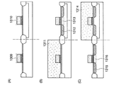
まず、図10(A)に示すように、基板1001の一表面に絶縁膜1002を介して剥離層1003を形成し、続けて下地膜として機能する絶縁膜1004と半導体膜1005(例えば、非晶質珪素を含む膜)を積層して形成する。なお、絶縁膜1002、剥離層1003、絶縁膜1004および半導体膜1005は、連続して形成することができる。
First, as shown in FIG. 10A, a
なお、基板1001は、ガラス基板、石英基板、金属基板(例えばステンレス基板など)、セラミック基板、Si基板等の半導体基板から選択されるものである。他にもプラスチック基板として、ポリエチレンテレフタレート(PET)、ポリエチレンナフタレート(PEN)、ポリエーテルサルフォン(PES)、アクリルなどの基板を選択することもできる。なお、本工程では、剥離層1003は、絶縁膜1002を介して基板1001の全面に設けているが、必要に応じて、基板1001の全面に剥離層を設けた後に、フォトリソグラフィ法により選択的に設けてもよい。
The
また、絶縁膜1002、絶縁膜1004は、CVD法やスパッタリング法等を用いて、酸化シリコン、窒化シリコン、酸化窒化シリコン(SiOxNy)(x>y>0)、窒化酸化シリコン(SiNxOy)(x>y>0)等の絶縁材料を用いて形成する。例えば、絶縁膜1002、1004を2層構造とする場合、第1層目の絶縁膜として窒化酸化シリコン膜を形成し、第2層目の絶縁膜として酸化窒化シリコン膜を形成するとよい。また、第1層目の絶縁膜として窒化シリコン膜を形成し、第2層目の絶縁膜として酸化シリコン膜を形成してもよい。絶縁膜1002は、基板1001から剥離層1003又はその上に形成される素子に不純物元素が混入するのを防ぐブロッキング層として機能し、絶縁膜1004は基板1001、剥離層1003からその上に形成される素子に不純物元素が混入するのを防ぐブロッキング層として機能する。このように、ブロッキング層として機能する絶縁膜1002、1004を形成することによって、基板1001からNaなどのアルカリ金属やアルカリ土類金属が、剥離層1003から剥離層に含まれる不純物元素がこの上に形成する素子に悪影響を与えることを防ぐことができる。なお、基板1001として石英を用いるような場合には絶縁膜1002、1004を省略してもよい。
The insulating
また、剥離層1003は、金属膜や金属膜と金属酸化膜の積層構造等を用いることができる。金属膜としては、タングステン(W)、モリブデン(Mo)、チタン(Ti)、タンタル(Ta)、ニオブ(Nb)、ニッケル(Ni)、コバルト(Co)、ジルコニウム(Zr)、亜鉛(Zn)、ルテニウム(Ru)、ロジウム(Rh)、パラジウム(Pd)、オスミウム(Os)、イリジウム(Ir)から選択された元素または当該元素を主成分とする合金材料若しくは化合物材料からなる膜を単層又は積層して形成する。また、これらの材料は、スパッタ法やプラズマCVD法等の各種CVD法等を用いて形成することができる。金属膜と金属酸化膜の積層構造としては、上述した金属膜を形成した後に、酸素雰囲気下またはN2O雰囲気下におけるプラズマ処理、酸素雰囲気下またはN2O雰囲気下における加熱処理を行うことによって、金属膜表面に当該金属膜の酸化物または酸化窒化物を設けることができる。例えば、金属膜としてスパッタ法やCVD法等によりタングステン膜を設けた場合、タングステン膜にプラズマ処理を行うことによって、タングステン膜表面にタングステン酸化物からなる金属酸化膜を形成することができる。また、この場合、タングステンの酸化物は、WOxで表され、Xは2〜3であり、Xが2の場合(WO2)、Xが2.5の場合(W2O5)、Xが2.75の場合(W4O11)、Xが3の場合(WO3)などがある。タングステンの酸化物を形成するにあたり、上記に挙げたXの値に特に制約はなく、エッチングレート等を基に、どの酸化物を形成するかを決めるとよい。他にも、例えば、金属膜(例えば、タングステン)を形成した後に、当該金属膜上にスパッタ法で酸化珪素(SiO2)等の絶縁膜を設けると共に、金属膜上に金属酸化物(例えば、タングステン上にタングステン酸化物)を形成してもよい。また、プラズマ処理として、例えば高密度プラズマ処理を行ってもよい。また、金属酸化膜の他にも、金属窒化物や金属酸化窒化物を用いてもよい。この場合、金属膜に窒素雰囲気下または窒素と酸素雰囲気下でプラズマ処理や加熱処理を行えばよい。
For the
また、半導体膜1005は、スパッタリング法、LPCVD法、プラズマCVD法等により、25〜200nm(好ましくは30〜150nm)の厚さで形成する。
The
次に、図10(B)に示すように、半導体膜1005にレーザー光を照射して結晶化を行う。なお、レーザー光の照射と、RTA又はファーネスアニール炉を用いる熱結晶化法、結晶化を助長する金属元素を用いる熱結晶化法とを組み合わせた方法等により半導体膜1005の結晶化を行ってもよい。その後、得られた半導体膜を所望の形状にエッチングして、結晶化した半導体膜1005a〜1005fを形成し、当該半導体膜1005a〜1005fを覆うようにゲート絶縁膜1006を形成する。
Next, as illustrated in FIG. 10B, the
なお、ゲート絶縁膜1006は、CVD法やスパッタリング法等を用いて、酸化シリコン、窒化シリコン、酸化窒化シリコン(SiOxNy)(x>y>0)、窒化酸化シリコン(SiNxOy)(x>y>0)等の絶縁材料を用いて形成する。例えば、ゲート絶縁膜1006を2層構造とする場合、第1層目の絶縁膜として酸化窒化シリコン膜を形成し、第2層目の絶縁膜として窒化酸化シリコン膜を形成するとよい。また、第1層目の絶縁膜として酸化シリコン膜を形成し、第2層目の絶縁膜として窒化シリコン膜を形成してもよい。
Note that the
半導体膜1005a〜1005fの作製工程の一例を以下に簡単に説明すると、まず、プラズマCVD法を用いて、膜厚50〜60nmの非晶質半導体膜を形成する。次に、結晶化を助長する金属元素であるニッケルを含む溶液を非晶質半導体膜上に保持させた後、非晶質半導体膜に脱水素化の処理(500℃、1時間)と、熱結晶化の処理(550℃、4時間)を行って結晶質半導体膜を形成する。その後、レーザー光を照射し、フォトリソグラフィ法を用いることよって結晶化された半導体膜1005a〜1005fを形成する。なお、結晶化を助長する金属元素を用いる熱結晶化を行わずに、レーザー光の照射だけで非晶質半導体膜の結晶化を行ってもよい。
An example of a manufacturing process of the
なお、結晶化に用いるレーザー発振器としては、連続発振型のレーザービーム(CWレーザービーム)やパルス発振型のレーザービーム(パルスレーザービーム)を用いることができる。ここで用いることができるレーザービームは、Arレーザー、Krレーザー、エキシマレーザーなどの気体レーザー、単結晶のYAG、YVO4、フォルステライト(Mg2SiO4)、YAlO3、GdVO4、若しくは多結晶(セラミック)のYAG、Y2O3、YVO4、YAlO3、GdVO4に、ドーパントとしてNd、Yb、Cr、Ti、Ho、Er、Tm、Taのうち1種または複数種添加されているものを媒質とするレーザー、ガラスレーザー、ルビーレーザー、アレキサンドライトレーザー、Ti:サファイアレーザー、銅蒸気レーザーまたは金蒸気レーザーのうち一種または複数種から発振されるものを用いることができる。このようなレーザービームの基本波、及びこれらの基本波の第2高調波から第4高調波のレーザービームを照射することで、大粒径の結晶を得ることができる。例えば、Nd:YVO4レーザー(基本波1064nm)の第2高調波(532nm)や第3高調波(355nm)を用いることができる。このときレーザーのパワー密度は0.01〜100MW/cm2程度(好ましくは0.1〜10MW/cm2)が必要である。そして、走査速度を10〜2000cm/sec程度として照射する。なお、単結晶のYAG、YVO4、フォルステライト(Mg2SiO4)、YAlO3、GdVO4、若しくは多結晶(セラミック)のYAG、Y2O3、YVO4、YAlO3、GdVO4に、ドーパントとしてNd、Yb、Cr、Ti、Ho、Er、Tm、Taのうち1種または複数種添加されているものを媒質とするレーザー、Arイオンレーザー、またはTi:サファイアレーザーは、連続発振をさせることが可能であり、Qスイッチ動作やモード同期などを行うことによって10MHz以上の発振周波数でパルス発振をさせることも可能である。10MHz以上の発振周波数でレーザービームを発振させると、半導体膜がレーザーによって溶融してから固化するまでの間に、次のパルスが半導体膜に照射される。従って、発振周波数が低いパルスレーザーを用いる場合と異なり、半導体膜中において固液界面を連続的に移動させることができるため、走査方向に向かって連続的に成長した結晶粒を得ることができる。 Note that as a laser oscillator used for crystallization, a continuous wave laser beam (CW laser beam) or a pulsed laser beam (pulse laser beam) can be used. The laser beam that can be used here is a gas laser such as Ar laser, Kr laser, or excimer laser, single crystal YAG, YVO 4 , forsterite (Mg 2 SiO 4 ), YAlO 3 , GdVO 4 , or polycrystalline ( (Ceramics) YAG, Y 2 O 3 , YVO 4 , YAlO 3 , GdVO 4 with one or more of Nd, Yb, Cr, Ti, Ho, Er, Tm, Ta added as dopants Lasers oscillated from one or more of laser, glass laser, ruby laser, alexandrite laser, Ti: sapphire laser, copper vapor laser or gold vapor laser as a medium can be used. By irradiating the fundamental wave of such a laser beam and the second to fourth harmonics of these fundamental waves, a crystal having a large grain size can be obtained. For example, the second harmonic (532 nm) or the third harmonic (355 nm) of an Nd: YVO 4 laser (fundamental wave 1064 nm) can be used. In this case, a laser power density is about 0.01 to 100 MW / cm 2 (preferably 0.1 to 10 MW / cm 2) is required. Then, irradiation is performed at a scanning speed of about 10 to 2000 cm / sec. Note that single crystal YAG, YVO 4 , forsterite (Mg 2 SiO 4 ), YAlO 3 , GdVO 4 , or polycrystalline (ceramic) YAG, Y 2 O 3 , YVO 4 , YAlO 3 , GdVO 4 , dopants Nd, Yb, Cr, Ti, Ho, Er, Tm, Ta as a medium, a laser, Ar ion laser, or Ti: sapphire laser with one or more added as a medium should be continuously oscillated It is also possible to perform pulse oscillation at an oscillation frequency of 10 MHz or more by performing Q switch operation, mode synchronization, or the like. When a laser beam is oscillated at an oscillation frequency of 10 MHz or higher, the semiconductor film is irradiated with the next pulse during the period from when the semiconductor film is melted by the laser to solidification. Therefore, unlike the case of using a pulse laser having a low oscillation frequency, the solid-liquid interface can be continuously moved in the semiconductor film, so that crystal grains continuously grown in the scanning direction can be obtained.
また、ゲート絶縁膜1006は、半導体膜1005a〜1005fに対し高密度プラズマ処理を行い、表面を酸化又は窒化することで形成しても良い。例えば、He、Ar、Kr、Xeなどの希ガスと、酸素、酸化窒素(NO2)、アンモニア、窒素、水素などの混合ガスを導入したプラズマ処理で形成する。この場合のプラズマの励起は、マイクロ波の導入により行うと、低電子温度で高密度のプラズマを生成することができる。この高密度プラズマで生成された酸素ラジカル(OHラジカルを含む場合もある)や窒素ラジカル(NHラジカルを含む場合もある)によって、半導体膜の表面を酸化又は窒化することができる。
Alternatively, the
このような高密度プラズマを用いた処理により、1〜20nm、代表的には5〜10nmの絶縁膜が半導体膜に形成される。この場合の反応は、固相反応であるため、当該絶縁膜と半導体膜との界面準位密度はきわめて低くすることができる。このような、高密度プラズマ処理は、半導体膜(結晶性シリコン、或いは多結晶シリコン)を直接酸化(若しくは窒化)するため、形成される絶縁膜の厚さは理想的には、ばらつきをきわめて小さくすることができる。加えて、結晶性シリコンの結晶粒界でも酸化が強くされることがないため、非常に好ましい状態となる。すなわち、ここで示す高密度プラズマ処理で半導体膜の表面を固相酸化することにより、結晶粒界において異常に酸化反応をさせることなく、均一性が良く、界面準位密度が低い絶縁膜を形成することができる。 By such treatment using high-density plasma, an insulating film with a thickness of 1 to 20 nm, typically 5 to 10 nm, is formed over the semiconductor film. Since the reaction in this case is a solid-phase reaction, the interface state density between the insulating film and the semiconductor film can be extremely low. Such high-density plasma treatment directly oxidizes (or nitrides) a semiconductor film (crystalline silicon or polycrystalline silicon), so that the thickness of the formed insulating film ideally has extremely small variation. can do. In addition, since oxidation is not strengthened even at the crystal grain boundaries of crystalline silicon, a very favorable state is obtained. That is, the surface of the semiconductor film is solid-phase oxidized by the high-density plasma treatment shown here, thereby forming an insulating film with good uniformity and low interface state density without causing an abnormal oxidation reaction at the grain boundaries. can do.
なお、ゲート絶縁膜1006は、高密度プラズマ処理によって形成される絶縁膜のみを用いても良いし、それにプラズマや熱反応を利用したCVD法で酸化シリコン、酸窒化シリコン、窒化シリコンなどの絶縁膜を堆積し、積層させても良い。もちろん、CVD法で酸化シリコン、酸窒化シリコン、窒化シリコンなどの絶縁膜を堆積し、この膜に対し高密後プラズマ処理を施しても良い。いずれにしても、高密度プラズマで形成した絶縁膜をゲート絶縁膜の一部又は全部に含んで形成されるトランジスタは、特性のばらつきを小さくすることができる。
Note that only an insulating film formed by high-density plasma treatment may be used as the
また、半導体膜に対し、連続発振レーザー若しくは10MHz以上の周波数で発振するレーザービームを照射しながら一方向に走査して結晶化させて得られた半導体膜1005a〜1005fは、そのビームの走査方向に結晶が成長する特性がある。その走査方向をチャネル長方向(チャネル形成領域が形成されたときにキャリアが流れる方向)に合わせてトランジスタを配置し、上記ゲート絶縁層を組み合わせることで、特性ばらつきが小さく、しかも電界効果移動度が高い薄膜トランジスタ(TFT:Thin Film Transistor)を得ることができる。
Further, the
次に、ゲート絶縁膜1006上に、第1の導電膜と第2の導電膜とを積層して形成する。ここでは、第1の導電膜は、CVD法やスパッタリング法等により、20〜100nmの厚さで形成する。第2の導電膜は、100〜400nmの厚さで形成する。第1の導電膜と第2の導電膜は、タンタル(Ta)、タングステン(W)、チタン(Ti)、モリブデン(Mo)、アルミニウム(Al)、銅(Cu)、クロム(Cr)、ニオブ(Nb)等から選択された元素又はこれらの元素を主成分とする合金材料若しくは化合物材料で形成する。また、リン等の不純物元素をドーピングした多結晶珪素に代表される半導体材料により形成しても良い。第1の導電膜と第2の導電膜の組み合わせの例を挙げると、窒化タンタル膜とタングステン膜、窒化タングステン膜とタングステン膜、窒化モリブデン膜とモリブデン膜等が挙げられる。タングステンや窒化タンタルは、耐熱性が高いため、第1の導電膜と第2の導電膜を形成した後に、熱活性化を目的とした加熱処理を行うことができる。また、2層構造ではなく、3層構造の場合は、モリブデン膜とアルミニウム膜とモリブデン膜の積層構造を採用するとよい。
Next, a first conductive film and a second conductive film are stacked over the
次に、フォトリソグラフィ法を用いてレジストからなるマスクを形成し、ゲート電極とゲート線を形成するためのエッチング処理を行って、半導体膜1005a〜1005fの上方にゲート電極1007を形成する。ここでは、ゲート電極1007として、第1の導電膜1007aと第2の導電膜1007bの積層構造で設けた例を示しているが、積層数には特に限定はない。
Next, a resist mask is formed using a photolithography method, and an etching process is performed to form the gate electrode and the gate line, so that the
次に、図10(C)に示すように、ゲート電極1007をマスクとして半導体膜1005a〜1005fに、イオンドープ法またはイオン注入法により、n型を付与する不純物元素を低濃度に添加し、その後、フォトリソグラフィ法によりレジストからなるマスクを選択的に形成して、p型を付与する不純物元素を高濃度に添加する。n型を示す不純物元素としては、リン(P)やヒ素(As)等を用いることができる。p型を示す不純物元素としては、ボロン(B)やアルミニウム(Al)やガリウム(Ga)等を用いることができる。ここでは、n型を付与する不純物元素としてリン(P)を用い、1×10¹⁵〜1×10¹⁹/cm3の濃度で含まれるように半導体膜1005a〜1005fに選択的に導入し、n型を示す不純物領域1008を形成する。また、p型を付与する不純物元素としてボロン(B)を用い、1×1019〜1×1020/cm3の濃度で含まれるように選択的に半導体膜1005c、1005eに導入し、p型を示す不純物領域1009を形成する。
Next, as illustrated in FIG. 10C, an impurity element imparting n-type conductivity is added to the
続いて、ゲート絶縁膜1006とゲート電極1007を覆うように、絶縁膜を形成する。絶縁膜は、プラズマCVD法やスパッタリング法等により、珪素、珪素の酸化物又は珪素の窒化物等の無機材料を含む膜や、有機樹脂などの有機材料を含む膜を、単層又は積層して形成する。次に、絶縁膜を、垂直方向を主体とした異方性エッチングにより選択的にエッチングして、ゲート電極1007の側面に接する絶縁膜1010(サイドウォールともよばれる)を形成する。絶縁膜1010は、LDD(Lightly Doped Drain)領域を形成する際のドーピング用のマスクとして用いる。
Subsequently, an insulating film is formed so as to cover the
続いて、フォトリソグラフィ法により形成したレジストからなるマスクと、ゲート電極1007および絶縁膜1010をマスクとして用いて、半導体膜1005a、1005b、1005d、1005fにn型を付与する不純物元素を高濃度に添加して、n型を示す不純物領域1011を形成する。ここでは、n型を付与する不純物元素としてリン(P)を用い、1×10¹⁹〜1×10²⁰/cm3の濃度で含まれるように半導体膜1005a、1005b、1005d、1005fに選択的に導入し、不純物領域1008より高濃度のn型を示す不純物領域1011を形成する。
Subsequently, an impurity element imparting n-type conductivity is added to the
以上の工程により、図10(D)に示すように、nチャネル型薄膜トランジスタ1000a、1000b、1000d、1000fとpチャネル型薄膜トランジスタ1000c、1000eが形成される。なお、ここでは薄膜トランジスタ1000a、1000bは本発明の不揮発性メモリのメモリセルアレイ部に用いられる薄膜トランジスタであり、薄膜トランジスタ1000c〜1000eは半導体装置が有するその他の薄膜トランジスタを示している。なお、メモリセルアレイ部に用いられる薄膜トランジスタ1000a、1000b及び書き込み時に用いられる一部のトランジスタは他のトランジスタに比べ、高い電位が印加される。そのため、高耐圧なトランジスタであることが好ましい。よって、少なくとも薄膜トランジスタ1000a、1000bのチャネル長Lは他のトランジスタのチャネル長より長い方が良い。もちろん、薄膜トランジスタ1000c〜1000eも、本発明の不揮発性メモリを構成する薄膜トランジスタとして用いることも可能である。
Through the above steps, n-channel
なお、nチャネル型薄膜トランジスタ1000aは、ゲート電極1007と重なる半導体膜1005aの領域にチャネル形成領域が形成され、ゲート電極1007及び絶縁膜1010と重ならない領域にソース領域又はドレイン領域を形成する不純物領域1011が形成され、絶縁膜1010と重なる領域であってチャネル形成領域と不純物領域1011の間に低濃度不純物領域(LDD領域)が形成されている。また、nチャネル型薄膜トランジスタ1000b、1000d、1000fも同様にチャネル形成領域、低濃度不純物領域及び不純物領域1011が形成されている。
Note that in the n-channel
また、pチャネル型薄膜トランジスタ1000cは、ゲート電極1007と重なる半導体膜1005cの領域にチャネル形成領域が形成され、ゲート電極1007と重ならない領域にソース領域又はドレイン領域を形成する不純物領域1009が形成されている。また、pチャネル型薄膜トランジスタ1000eも同様にチャネル形成領域及び不純物領域1009が形成されている。なお、ここでは、pチャネル型薄膜トランジスタ1000c、1000eには、LDD領域を設けていないが、pチャネル型薄膜トランジスタにLDD領域を設けてもよいし、nチャネル型薄膜トランジスタにLDD領域を設けない構成としてもよい。
In the p-channel
次に、図11(A)に示すように、半導体膜1005a〜1005f、ゲート電極1007等を覆うように、絶縁膜を単層または積層して形成し、当該絶縁膜上に薄膜トランジスタ1000a〜1000fのソース領域又はドレイン領域を形成する不純物領域1009、1011と電気的に接続する導電膜1013を形成する。絶縁膜は、CVD法、スパッタリング法、SOG法、液滴吐出法、スクリーン印刷法等により、珪素の酸化物や珪素の窒化物等の無機材料、ポリイミド、ポリアミド、ベンゾシクロブテン、アクリル、エポキシ等の有機材料やシロキサン材料等により、単層または積層で形成する。ここでは、当該絶縁膜を2層で設け、1層目の絶縁膜1012aとして窒化酸化珪素膜で形成し、2層目の絶縁膜1012bとして酸化窒化珪素膜で形成する。また、導電膜1013は、薄膜トランジスタ1000a〜1000fのソース電極又はドレイン電極を形成する。
Next, as illustrated in FIG. 11A, an insulating film is formed as a single layer or a stacked layer so as to cover the
なお、絶縁膜1012a、1012bを形成する前、または絶縁膜1012a、1012bのうちの1つまたは複数の薄膜を形成した後に、半導体膜の結晶性の回復や半導体膜に添加された不純物元素の活性化、半導体膜の水素化を目的とした加熱処理を行うとよい。加熱処理には、熱アニール、レーザーアニール法またはRTA法などを適用するとよい。
Note that before the insulating
また、導電膜1013は、CVD法やスパッタリング法等により、アルミニウム(Al)、タングステン(W)、チタン(Ti)、タンタル(Ta)、モリブデン(Mo)、ニッケル(Ni)、白金(Pt)、銅(Cu)、金(Au)、銀(Ag)、マンガン(Mn)、ネオジム(Nd)、炭素(C)、シリコン(Si)から選択された元素、又はこれらの元素を主成分とする合金材料若しくは化合物材料で、単層又は積層で形成する。アルミニウムを主成分とする合金材料とは、例えば、アルミニウムを主成分としニッケルを含む材料、又は、アルミニウムを主成分とし、ニッケルと、炭素と珪素の一方又は両方とを含む合金材料に相当する。導電膜1013は、例えば、バリア膜とアルミニウムシリコン(Al−Si)膜とバリア膜の積層構造、バリア膜とアルミニウムシリコン(Al−Si)膜と窒化チタン膜とバリア膜の積層構造を採用するとよい。なお、バリア膜とは、チタン、チタンの窒化物、モリブデン、又はモリブデンの窒化物からなる薄膜に相当する。アルミニウムやアルミニウムシリコンは抵抗値が低く、安価であるため、導電膜1013を形成する材料として最適である。また、上層と下層のバリア層を設けると、アルミニウムやアルミニウムシリコンのヒロックの発生を防止することができる。また、還元性の高い元素であるチタンからなるバリア膜を形成すると、半導体膜上に薄い自然酸化膜ができていたとしても、この自然酸化膜を還元し、半導体膜と良好なコンタクトをとることができる。
The
次に、導電膜1013を覆うように絶縁膜1014を形成し、当該絶縁膜1014上に、薄膜トランジスタのソース電極又はドレイン電極を形成する導電膜1013と電気的に接続する導電膜1015a、1015bを形成する。図11(B)では、メモリセルアレイ部分を構成する薄膜トランジスタ1000a及び薄膜トランジスタ1000bのソース電極又はドレイン電極を形成する導電膜1013と電気的に接続された導電膜として導電膜1015aが、薄膜トランジスタ1000fのソース電極又はドレイン電極を形成する導電膜1013と電気的に接続された導電膜として導電膜1015bが図示されている。なお、導電膜1015aは後に形成される記憶素子の第1の電極として機能する。また、導電膜1015bは後に形成されるアンテナの下地膜として機能する。この導電膜1015bにより、薄膜トランジスタ1000fとアンテナとの接続をより確実に行うことや絶縁膜1014とアンテナとの密着性を向上させることができる。導電膜1015a及び導電膜1015bは、上述した導電膜1013で示したいずれかの材料を用いて形成することができる。
Next, an insulating
なお、絶縁膜1014は、CVD法やスパッタ法等により、酸化珪素(SiOx)、窒化珪素(SiNx)、酸化窒化珪素(SiOxNy)(x>y)、窒化酸化珪素(SiNxOy)(x>y)等の酸素または窒素を有する絶縁膜やDLC(ダイヤモンドライクカーボン)等の炭素を含む膜、エポキシ、ポリイミド、ポリアミド、ポリビニルフェノール、ベンゾシクロブテン、アクリル等の有機材料またはシロキサン樹脂等のシロキサン材料からなる単層または積層構造で設けることができる。なお、シロキサン材料とは、Si−O−Si結合を含む材料に相当する。シロキサンは、シリコン(Si)と酸素(O)との結合で骨格構造が構成される。置換基として、少なくとも水素を含む有機基(例えばアルキル基、アリール基)が用いられる。置換基として、フルオロ基を用いることもできる。または置換基として、少なくとも水素を含む有機基と、フルオロ基とを用いてもよい。
Note that the insulating
次に、メモリセルアレイ部分を構成する各々の記憶素子を分離するため、各記憶素子の第1の電極の間に隔壁(絶縁層)1016を形成する。なお、隔壁(絶縁層)1016の断面において、隔壁(絶縁層)1016の側面は、第1の電極の表面に対して10度以上60度未満、好ましくは25度以上45度以下の傾斜角度を有することが好ましい。さらには、湾曲していることが好ましい。 Next, partition walls (insulating layers) 1016 are formed between the first electrodes of the memory elements in order to separate the memory elements constituting the memory cell array portion. Note that in the cross section of the partition wall (insulating layer) 1016, the side surface of the partition wall (insulating layer) 1016 has an inclination angle of 10 degrees to less than 60 degrees, preferably 25 degrees to 45 degrees with respect to the surface of the first electrode. It is preferable to have. Furthermore, it is preferable that it is curved.
なお、隔壁(絶縁層)1016には、酸化珪素、窒化珪素、酸化窒化珪素、酸化アルミニウム、窒化アルミニウム、酸化窒化アルミニウムその他の無機絶縁性材料、又はアクリル酸、メタクリル酸及びこれらの誘導体、又はポリイミド、芳香族ポリアミド、ポリベンゾイミダゾールなどの耐熱性高分子、又はシロキサン材料を用いることができる。また、ポリビニルアルコール、ポリビニルブチラールなどのビニル樹脂、エポキシ樹脂、フェノール樹脂、ノボラック樹脂、アクリル樹脂、メラミン樹脂、ウレタン樹脂等の樹脂材料を用いることもできる。ベンゾシクロブテン、パリレン、ポリイミドなどの有機材料、重合によってできた化合物材料、水溶性ホモポリマーと水溶性共重合体を含む組成物材料等を用いてもよい。なお、作製法としては、CVD法、スパッタリング法、液滴吐出法、ディスペンサ法、印刷法等を用いることができる。また、スピンコート法で得られる薄膜なども用いることができる。 Note that the partition wall (insulating layer) 1016 includes silicon oxide, silicon nitride, silicon oxynitride, aluminum oxide, aluminum nitride, aluminum oxynitride, other inorganic insulating materials, acrylic acid, methacrylic acid, and derivatives thereof, or polyimide Further, a heat-resistant polymer such as aromatic polyamide or polybenzimidazole, or a siloxane material can be used. Moreover, resin materials, such as vinyl resins, such as polyvinyl alcohol and polyvinyl butyral, an epoxy resin, a phenol resin, a novolac resin, an acrylic resin, a melamine resin, and a urethane resin, can also be used. An organic material such as benzocyclobutene, parylene, or polyimide, a compound material obtained by polymerization, a composition material containing a water-soluble homopolymer and a water-soluble copolymer, or the like may be used. Note that as a manufacturing method, a CVD method, a sputtering method, a droplet discharge method, a dispenser method, a printing method, or the like can be used. A thin film obtained by a spin coating method can also be used.
次に、導電膜1015bと電気的に接続されるアンテナとして機能する導電膜1021を形成する。
Next, a
導電膜1021は、CVD法、スパッタリング法、スクリーン印刷やグラビア印刷等の印刷法、液滴吐出法、ディスペンサ法、メッキ法等を用いて、導電性材料により形成する。導電性材料は、アルミニウム(Al)、チタン(Ti)、銀(Ag)、銅(Cu)、金(Au)、白金(Pt)ニッケル(Ni)、パラジウム(Pd)、タンタル(Ta)、モリブデン(Mo)から選択された元素、又はこれらの元素を主成分とする合金材料若しくは化合物材料で、単層構造又は積層構造で形成する。
The
例えば、スクリーン印刷法を用いてアンテナとして機能する導電膜1021を形成する場合には、粒径が数nmから数十μmの導電体粒子を有機樹脂に溶解または分散させた導電性のペーストを選択的に印刷することによって設けることができる。導電体粒子としては、銀(Ag)、金(Au)、銅(Cu)、ニッケル(Ni)、白金(Pt)、パラジウム(Pd)、タンタル(Ta)、モリブデン(Mo)およびチタン(Ti)等のいずれか一つ以上の金属粒子やハロゲン化銀の微粒子、または分散性ナノ粒子を用いることができる。また、導電性ペーストに含まれる有機樹脂は、金属粒子のバインダー、溶媒、分散剤および被覆材として機能する有機樹脂から選ばれた一つまたは複数を用いることができる。代表的には、エポキシ樹脂、シリコーン樹脂等の有機樹脂が挙げられる。また、導電膜の形成にあたり、導電性のペーストを押し出した後に焼成することが好ましい。例えば、導電性のペーストの材料として、銀を主成分とする微粒子(例えば粒径1nm以上100nm以下)を用いる場合、150〜300℃の温度範囲で焼成することにより硬化させて導電膜を得ることができる。また、はんだや鉛フリーのはんだを主成分とする微粒子を用いてもよく、この場合は粒径20μm以下の微粒子を用いることが好ましい。はんだや鉛フリーはんだは、低コストであるといった利点を有している。
For example, when the
次に、メモリセルアレイ部分を構成する記憶素子を形成する。まず、隔壁(絶縁層)1016及び記憶素子の第1の電極、即ち導電膜1015a上にメモリ層1017を形成する。ここでは、メモリ層1017として有機化合物層を用いた例について説明する。この有機化合物層は、電圧を印加することで第1の電極及び第2の電極の一部が接続、つまり短絡する性質を有する。よって、記憶素子に所定の電圧を印加することで高抵抗状態から低抵抗状態へ移行し、書き込む動作を行うことができる。なお、本実施例ではメモリ層1017として有機化合物層を用いた場合について述べるが、電圧の印加によって低抵抗状態へ移行することが可能な物質より形成された層であれば良い。
Next, a memory element constituting the memory cell array portion is formed. First, the
メモリ層1017に用いる有機化合物として、正孔輸送性もしくは電子輸送性を有する有機化合物を用いて形成することができる。なお、ここで正孔輸送性を有する化合物とは正孔のみを輸送するものではなく、電子輸送性も有するが、電子の移動度よりも正孔の移動度が大きい化合物を意味する。また、電子輸送性を有する化合物とは電子のみを輸送するものではなく、正孔輸送性も有するが、正孔の移動度よりも電子の移動度が大きい化合物を意味する。従って、正孔と電子の両方を輸送する材料もこれらの範疇に含まれる。
As the organic compound used for the
例えば、正孔輸送性を有する有機化合物としては、2,7−ジ(N−カルバゾリル)−スピロ−9,9’−ビフルオレン(略称:SFDCz)、4,4’−ビス[N−(1−ナフチル)−N−フェニルアミノ]ビフェニル(略称:NPB)や4,4’−ビス[N−(3−メチルフェニル)−N−フェニル−アミノ]−ビフェニル(略称:TPD)や4,4’,4’’−トリス(N,N−ジフェニル−アミノ)−トリフェニルアミン(略称:TDATA)、4,4’,4’’−トリス[N−(3−メチルフェニル)−N−フェニル−アミノ]−トリフェニルアミン(略称:MTDATA)や4,4’−ビス(N−(4−(N,N−ジ−m−トリルアミノ)フェニル)−N−フェニルアミノ)ビフェニル(略称:DNTPD)などの芳香族アミン系(即ち、ベンゼン環−窒素の結合を有する)の化合物やフタロシアニン(略称:H2Pc)、銅フタロシアニン(略称:CuPc)、バナジルフタロシアニン(略称:VOPc)のようなフタロシアニン化合物等が挙げられる。電子輸送性の高い有機化合物としては、トリス(8−キノリノラト)アルミニウム(略称:Alq)、トリス(4−メチル−8−キノリノラト)アルミニウム(略称:Almq3)、ビス(10−ヒドロキシベンゾ[h]−キノリナト)ベリリウム(略称:BeBq2)、ビス(2−メチル−8−キノリノラト)−4−フェニルフェノラト−アルミニウム(略称:BAlq)等キノリン骨格またはベンゾキノリン骨格を有する金属錯体等からなる材料を用いることができる。また、この他、ビス[2−(2−ヒドロキシフェニル)ベンゾオキサゾラト]亜鉛(略称:Zn(BOX)2)、ビス[2−(2−ヒドロキシフェニル)ベンゾチアゾラト]亜鉛(略称:Zn(BTZ)2)などのオキサゾール系、チアゾール系配位子を有する金属錯体などの材料も用いることができる。さらに、金属錯体以外にも、2−(4−ビフェニリル)−5−(4−tert−ブチルフェニル)−1,3,4−オキサジアゾール(略称:PBD)、1,3−ビス[5−(p−tert−ブチルフェニル)−1,3,4−オキサジアゾール−2−イル]ベンゼン(略称:OXD−7)、3−(4−tert−ブチルフェニル)−4−フェニル−5−(4−ビフェニリル)−1,2,4−トリアゾール(略称:TAZ)、3−(4−tert−ブチルフェニル)−4−(4−エチルフェニル)−5−(4−ビフェニリル)−1,2,4−トリアゾール(略称:p−EtTAZ)、バソフェナントロリン(略称:BPhen)、バソキュプロイン(略称:BCP)等が挙げられる。 For example, as an organic compound having a hole-transport property, 2,7-di (N-carbazolyl) -spiro-9,9′-bifluorene (abbreviation: SFDCz), 4,4′-bis [N- (1- Naphthyl) -N-phenylamino] biphenyl (abbreviation: NPB) or 4,4′-bis [N- (3-methylphenyl) -N-phenyl-amino] -biphenyl (abbreviation: TPD) or 4,4 ′, 4 ″ -tris (N, N-diphenyl-amino) -triphenylamine (abbreviation: TDATA), 4,4 ′, 4 ″ -tris [N- (3-methylphenyl) -N-phenyl-amino] Fragrances such as triphenylamine (abbreviation: MTDATA) and 4,4′-bis (N- (4- (N, N-di-m-tolylamino) phenyl) -N-phenylamino) biphenyl (abbreviation: DNTPD) Group amines (ie, ben Zen ring - having nitrogen bond) compounds and phthalocyanine (abbreviation: H 2 Pc), copper phthalocyanine (abbreviation: CuPc), or vanadyl phthalocyanine (abbreviation: VOPc), and phthalocyanine compounds, and the like, such as. Examples of the organic compound having a high electron-transport property include tris (8-quinolinolato) aluminum (abbreviation: Alq), tris (4-methyl-8-quinolinolato) aluminum (abbreviation: Almq 3 ), and bis (10-hydroxybenzo [h]. -Quinolinato) Beryllium (abbreviation: BeBq 2 ), bis (2-methyl-8-quinolinolato) -4-phenylphenolato-aluminum (abbreviation: BAlq), etc. Can be used. In addition, bis [2- (2-hydroxyphenyl) benzoxazolate] zinc (abbreviation: Zn (BOX) 2 ), bis [2- (2-hydroxyphenyl) benzothiazolate] zinc (abbreviation: Zn (BTZ) A material such as a metal complex having an oxazole-based or thiazole-based ligand such as 2 ) can also be used. In addition to metal complexes, 2- (4-biphenylyl) -5- (4-tert-butylphenyl) -1,3,4-oxadiazole (abbreviation: PBD), 1,3-bis [5- (P-tert-butylphenyl) -1,3,4-oxadiazol-2-yl] benzene (abbreviation: OXD-7), 3- (4-tert-butylphenyl) -4-phenyl-5- ( 4-biphenylyl) -1,2,4-triazole (abbreviation: TAZ), 3- (4-tert-butylphenyl) -4- (4-ethylphenyl) -5- (4-biphenylyl) -1,2, 4-triazole (abbreviation: p-EtTAZ), bathophenanthroline (abbreviation: BPhen), bathocuproin (abbreviation: BCP), and the like can be given.
上記の他、例えば2,3−ビス(4−ジフェニルアミノフェニル)キノキサリン(略称:TPAQn)、1,3,5−トリ(N−カルバゾリル)ベンゼン(略称:TCzB)、9−[4−(N−カルバゾリル)]フェニル−10−フェニルアントラセン(略称:CzPA)、3,6−ジフェニル−9−[4−(10−フェニル−9−アントリル)フェニル]−9H−カルバゾール(略称:DPCzPA)、2−t−ブチル−9、10−ビス(4−(N−カルバゾリル)フェニル)アントラセン(略称:CzBPA)、3−[N−(9−フェニルカルバゾール−3−イル)−N−フェニルアミノ]−9−フェニルカルバゾール(略称:PCzPCA1)、3,6−ビス[N−(9−フェニルカルバゾール−3−イル)−N−フェニルアミノ]−9−フェニルカルバゾール(略称:PCzPCA2)、3−[N−(1−ナフチル)−N−(9−フェニルカルバゾール−3−イル)アミノ]−9−フェニルカルバゾール(略称:PCzPCN1)、4,4’−ジ(N−カルバゾリル)ビフェニル(略称:CBP)、1,3,5−トリス[4−(N−カルバゾリル)フェニル]ベンゼン(略称:TCPB)、N−(2−ナフチル)カルバゾール(略称:NCz)等を用いて形成してもよい。 In addition to the above, for example, 2,3-bis (4-diphenylaminophenyl) quinoxaline (abbreviation: TPAQn), 1,3,5-tri (N-carbazolyl) benzene (abbreviation: TCzB), 9- [4- (N -Carbazolyl)] phenyl-10-phenylanthracene (abbreviation: CzPA), 3,6-diphenyl-9- [4- (10-phenyl-9-anthryl) phenyl] -9H-carbazole (abbreviation: DPCzPA), 2- t-butyl-9,10-bis (4- (N-carbazolyl) phenyl) anthracene (abbreviation: CzBPA), 3- [N- (9-phenylcarbazol-3-yl) -N-phenylamino] -9- Phenylcarbazole (abbreviation: PCzPCA1), 3,6-bis [N- (9-phenylcarbazol-3-yl) -N-phenylamino]- -Phenylcarbazole (abbreviation: PCzPCA2), 3- [N- (1-naphthyl) -N- (9-phenylcarbazol-3-yl) amino] -9-phenylcarbazole (abbreviation: PCzPCN1), 4,4'- Di (N-carbazolyl) biphenyl (abbreviation: CBP), 1,3,5-tris [4- (N-carbazolyl) phenyl] benzene (abbreviation: TCPB), N- (2-naphthyl) carbazole (abbreviation: NCz) Etc. may be used.
また、有機化合物層は、蒸着法、電子ビーム蒸着法、スパッタ法、CVD法等を用いて形成することができる。また、他の形成方法として、スピンコート法、ゾル−ゲル法、印刷法または液滴吐出法等を用いてもよいし、上記方法とこれらを組み合わせてもよい。 The organic compound layer can be formed using a vapor deposition method, an electron beam vapor deposition method, a sputtering method, a CVD method, or the like. In addition, as another forming method, a spin coating method, a sol-gel method, a printing method, a droplet discharge method, or the like may be used, or the above method may be combined with these methods.
また、有機化合物層には、正孔輸送性もしくは電子輸送性を有する有機化合物に絶縁物が混合されていても良いし、第1の電極とメモリ層との間に半導体層を有していても良い。 In addition, the organic compound layer may have an insulator mixed with an organic compound having a hole transporting property or an electron transporting property, and may have a semiconductor layer between the first electrode and the memory layer. Also good.
次に、メモリ層1017上に第2の電極として機能する導電膜1018を形成する。この導電膜1018は、上述した導電膜1013で示したいずれかの材料を用いて形成することができる。
Next, a
以上のようにして、第1の電極として機能する導電膜1015aと、メモリ層1017と、第2の電極として機能する導電膜1018とを有する記憶素子1019a、1019bを形成することができる。なお、これらの記憶素子は、隔壁(絶縁層)1016によって分離されており、隣接する記憶素子間への電界の影響を防止するだけではなく、メモリ層1017を設ける際に導電膜1015aの段差により生じるメモリ層1017の段切れを隔壁(絶縁層)1016を用いて防止することができる。なお、隔壁(絶縁層)1016を設けずにメモリ層1017が隣接する記憶素子間で分離できる構成としている場合には特に設ける必要はない。
As described above, the
次に、図11(C)に示すように、導電膜1021や記憶素子1019a、1019bを覆うように絶縁膜1022を形成した後、薄膜トランジスタ1000a〜1000f、導電膜1021、記憶素子1019a、1019b等を含む層(以下、「素子形成層10」と記す)を基板1001から剥離する。ここでは、レーザー光(例えばUV光)を照射することによって、薄膜トランジスタ1000a〜1000fを避けた領域に開口部を形成後、物理的な力を用いて基板1001から素子形成層10を剥離することができる。また、基板1001から素子形成層10を剥離する前に、形成した開口部にエッチング剤を導入して、剥離層1003を選択的に除去してもよい。エッチング剤は、フッ化ハロゲンまたはハロゲン間化合物を含む気体又は液体を使用する。例えば、フッ化ハロゲンを含む気体として三フッ化塩素(ClF3)を使用する。そうすると、素子形成層10は、基板1001から剥離された状態となる。なお、剥離層1003は、全て除去せず一部分を残存させてもよい。こうすることによって、エッチング剤の消費量を抑え剥離層の除去に要する処理時間を短縮することが可能となる。また、剥離層1003の除去を行った後にも、基板1001上に素子形成層10を保持しておくことが可能となる。また、素子形成層10が剥離された基板1001を再利用することによって、コストの削減をすることができる。
Next, as illustrated in FIG. 11C, an insulating
絶縁膜1022は、CVD法やスパッタ法等により、酸化珪素(SiOx)、窒化珪素(SiNx)、酸化窒化珪素(SiOxNy)(x>y)、窒化酸化珪素(SiNxOy)(x>y)等の酸素または窒素を有する絶縁膜やDLC(ダイヤモンドライクカーボン)等の炭素を含む膜、エポキシ、ポリイミド、ポリアミド、ポリビニルフェノール、ベンゾシクロブテン、アクリル等の有機材料またはシロキサン樹脂等のシロキサン材料からなる単層または積層構造で設けることができる。
The insulating
本実施例では、図12(A)に示すように、レーザー光の照射により素子形成層10に開口部を形成した後に、当該素子形成層10の一方の面(絶縁膜1022の露出した面)に第1のシート材1023を貼り合わせた後、基板1001から素子形成層10を剥離する。
In this embodiment, as shown in FIG. 12A, after an opening is formed in the
次に、図12(B)に示すように、素子形成層10の他方の面(剥離により露出した面)に、加熱処理と加圧処理の一方又は両方を行って第2のシート材1024を貼り合わせる。なお、第1のシート材1023、第2のシート材1024として、ホットメルトフィルム等を用いることができる。
Next, as illustrated in FIG. 12B, one or both of heat treatment and pressure treatment is performed on the other surface of the element formation layer 10 (surface exposed by peeling) to form the
また、第1のシート材1023、第2のシート材1024として、静電気等を防止する帯電防止対策を施したフィルム(以下、帯電防止フィルムと記す)を用いることもできる。帯電防止フィルムとしては、帯電防止可能な材料を樹脂中に分散させたフィルム、及び帯電防止可能な材料が貼り付けられたフィルム等が挙げられる。帯電防止可能な材料が設けられたフィルムは、片面に帯電防止可能な材料を設けたフィルムであってもよいし、両面に帯電防止可能な材料を設けたフィルムであってもよい。さらに、片面に帯電防止可能な材料が設けられたフィルムは、帯電防止可能な材料が設けられた面をフィルムの内側になるように層に貼り付けてもよいし、フィルムの外側になるように貼り付けてもよい。なお、帯電防止可能な材料はフィルムの全面、あるいは一部に設けてあればよい。ここでの帯電防止可能な材料としては、金属、インジウムと錫の酸化物(ITO:Indium Tin Oxide)、両性界面活性剤や陽イオン性界面活性剤や非イオン性界面活性剤等の界面活性剤用いることができる。また、他にも帯電防止材料として、側鎖にカルボキシル基および4級アンモニウム塩基をもつ架橋性共重合体高分子を含む樹脂材料等を用いることができる。これらの材料をフィルムに貼り付けたり、練り込んだり、塗布することによって帯電防止フィルムとすることができる。帯電防止フィルムで封止を行うことによって、商品として取り扱う際に、外部からの静電気等によって半導体素子に悪影響が及ぶことを抑制することができる。
In addition, as the first sheet material 1023 and the
以上の工程により、本発明の不揮発性メモリを有する半導体装置を作製することができる。なお、本実施例では、アンテナを薄膜トランジスタと同じ基板上に形成している例について説明したが、本発明はこの構成に限定されない。薄膜トランジスタを有する層が形成される第1の基板と、アンテナとして機能する導電層が形成される第2の基板とを導電性粒子を含む樹脂により貼り合わせることで、薄膜トランジスタとアンテナとを電気的に接続してもよい。 Through the above steps, a semiconductor device having the nonvolatile memory of the present invention can be manufactured. Note that although an example in which the antenna is formed over the same substrate as the thin film transistor has been described in this embodiment, the present invention is not limited to this structure. The thin film transistor and the antenna are electrically connected to each other by bonding a first substrate over which a layer having a thin film transistor is formed and a second substrate over which a conductive layer functioning as an antenna is formed using a resin containing conductive particles. You may connect.
また、上記では基板上に薄膜トランジスタ等の素子を形成した後に剥離する工程を示したが、剥離を行わずそのまま製品としてもよい。また、ガラス基板上に薄膜トランジスタ等の素子を設けた後に、当該ガラス基板を素子が設けられた面と反対側から研磨することにより半導体装置の薄膜化、小型化を行うことができる。 Moreover, although the process which peeled after forming elements, such as a thin film transistor, on the board | substrate was shown above, it is good also as a product as it is, without peeling. Further, after an element such as a thin film transistor is provided over a glass substrate, the semiconductor substrate can be thinned and miniaturized by polishing the glass substrate from the side opposite to the surface on which the element is provided.
また、本実施例は本明細書中の実施の形態及び他の実施例の記載と適宜組み合わせることが可能である。 In addition, this embodiment can be combined with the description of the embodiment mode and other embodiments in this specification as appropriate.
本実施例では、上記実施例とは異なる本発明の不揮発性メモリもしくは半導体装置が有するトランジスタの作製方法について説明する。本発明の不揮発性メモリもしくは半導体装置が有するトランジスタは、上記実施例で説明した絶縁基板上の薄膜トランジスタの他、単結晶基板上のMOSトランジスタで構成することもできる。 In this embodiment, a method for manufacturing a transistor included in the nonvolatile memory or the semiconductor device of the present invention, which is different from the above embodiment, will be described. The transistor included in the nonvolatile memory or the semiconductor device of the present invention can be formed using a MOS transistor on a single crystal substrate in addition to the thin film transistor on the insulating substrate described in the above embodiment.
本実施例では、本発明の不揮発性メモリもしくは半導体装置が有するトランジスタの作製方法の一例に関して、図13乃至図15に示す部分断面図を用いて説明する。 In this embodiment, an example of a method for manufacturing a transistor included in the nonvolatile memory or the semiconductor device of the present invention will be described with reference to partial cross-sectional views shown in FIGS.
まず、半導体基板1300に素子を分離した領域1302、1303(以下、領域1302、1303とも記す)を形成する(図13(A)参照)。半導体基板1300に設けられた領域1302、1303は、それぞれ絶縁膜1301(フィールド酸化膜ともいう)によって分離されている。なお、ここでは、半導体基板1300としてn型の導電型を有する単結晶Si基板を用い、半導体基板1300の領域1303にpウェル1304を設けた例を示している。
First,
基板1300は、半導体基板であれば特に限定されず用いることができる。例えば、n型又はp型の導電型を有する単結晶Si基板、化合物半導体基板(GaAs基板、InP基板、GaN基板、SiC基板、サファイア基板、ZnSe基板等)、貼り合わせ法またはSIMOX(Separation by Implanted Oxygen)法を用いて作製されたSOI(Silicon on Insulator)基板等を用いることができる。
The
素子分離領域1302、1303は、選択酸化法(LOCOS(Local Oxidation of Silicon)法)又はトレンチ分離法等を適宜用いることができる。
For the
また、半導体基板1300の領域1303に形成されたpウェルは、半導体基板1300にp型の導電型を有する不純物元素を選択的に導入することによって形成することができる。p型を示す不純物元素としては、ボロン(B)やアルミニウム(Al)やガリウム(Ga)等を用いることができる。
The p-well formed in the
なお、本実施例では、半導体基板1300としてn型の導電型を有する半導体基板を用いているため、領域1302には不純物元素の導入を行っていないが、n型を示す不純物元素を導入することにより領域1302にnウェルを形成してもよい。n型を示す不純物元素としては、リン(P)やヒ素(As)等を用いることができる。一方、p型の導電型を有する半導体基板を用いる場合には、領域1302にn型を示す不純物元素を導入してnウェルを形成し、領域1303には不純物元素の導入を行わない構成としてもよい。
Note that in this embodiment, since a semiconductor substrate having n-type conductivity is used as the
次に、図13(B)に示すように領域1302、1303を覆うように絶縁膜1305、1306をそれぞれ形成する。
Next, as illustrated in FIG. 13B, insulating
絶縁膜1305、1306は、例えば、熱処理を行い半導体基板1300に設けられた領域1302、1303の表面を酸化させることにより酸化珪素膜で形成することができる。また、熱酸化法により酸化珪素膜を形成した後に、窒化処理を行うことによって酸化珪素膜の表面を窒化させることにより、酸化珪素膜と酸素と窒素を有する膜(酸窒化珪素膜)との積層構造で形成してもよい。
The insulating
他にも、上述したように、プラズマ処理を用いて絶縁膜1305、1306を形成してもよい。例えば、半導体基板1300に設けられた領域1302、1303の表面に高密度プラズマ処理により酸化処理又は窒化処理を行うことにより、絶縁膜1305、1306として酸化珪素(SiOx)膜又は窒化珪素(SiNx)膜で形成することができる。また、高密度プラズマ処理により領域1302、1303の表面に酸化処理を行った後に、再度高密度プラズマ処理を行うことによって窒化処理を行ってもよい。この場合、領域1302、1303の表面に接して酸化珪素膜が形成され、当該酸化珪素膜上に酸窒化珪素膜が形成され、絶縁膜1305、1306は酸化珪素膜と酸窒化珪素膜とが積層された膜となる。また、熱酸化法により領域1302、1303の表面に酸化珪素膜を形成した後に高密度プラズマ処理により酸化処理又は窒化処理を行ってもよい。
In addition, as described above, the insulating
なお、絶縁膜1305、1306は、後に完成されるトランジスタにおいてゲート絶縁膜として機能する。
Note that the insulating
次に、図13(C)に示すように領域1302、1303の上方に形成された絶縁膜1305、1306を覆うように導電膜を形成する。ここでは、導電膜として、導電膜1307と導電膜1308を順に積層して形成した例を示している。もちろん、導電膜は、単層又は3層以上の積層構造で形成してもよい。
Next, as illustrated in FIG. 13C, a conductive film is formed so as to cover the insulating
導電膜1307、1308としては、タンタル(Ta)、タングステン(W)、チタン(Ti)、モリブデン(Mo)、アルミニウム(Al)、銅(Cu)、クロム(Cr)、ニオブ(Nb)等から選択された元素またはこれらの元素を主成分とする合金材料若しくは化合物材料で形成することができる。また、これらの元素を窒化した金属窒化膜で形成することもできる。他にも、リン等の不純物元素をドーピングした多結晶珪素に代表される半導体材料により形成することもできる。
The
ここでは、導電膜1307として窒化タンタルを用いて形成し、その上に導電膜1308としてタングステンを用いて積層構造で設ける。また、他にも、導電膜1307として、窒化タングステン、窒化モリブデン又は窒化チタンから選ばれた単層又は積層膜を用い、導電膜1308として、タンタル、モリブデン、チタンから選ばれた単層又は積層膜を用いることができる。
Here, the
次に、積層して設けられた導電膜1307、1308を選択的にエッチングして除去することによって、領域1302、1303の上方の一部に導電膜1307、1308を残存させ、図14(A)に示すようにそれぞれゲート電極1309、1310を形成する。
Next, the
次に、領域1302を覆うようにレジストマスク1311を選択的に形成し、当該レジストマスク1311、ゲート電極1310をマスクとして領域1303に不純物元素を導入することによって不純物領域を形成する(図14(B)参照)。不純物元素としては、n型を付与する不純物元素又はp型を付与する不純物元素を用いる。n型を示す不純物元素としては、リン(P)やヒ素(As)等を用いることができる。p型を示す不純物元素としては、ボロン(B)やアルミニウム(Al)やガリウム(Ga)等を用いることができる。ここでは、不純物元素として、リン(P)を用いる。
Next, a resist
不純物元素を導入することによって、図14(B)に示すように領域1303にソース領域又はドレイン領域を形成する不純物領域1312とチャネル形成領域1313が形成される。
By introducing the impurity element, an
次に、図14(C)に示すように領域1303を覆うようにレジストマスク1314を選択的に形成し、当該レジストマスク1314、ゲート電極1309をマスクとして領域1302に不純物元素を導入することによって不純物領域を形成する。不純物元素としては、n型を付与する不純物元素又はp型を付与する不純物元素を用いる。n型を示す不純物元素としては、リン(P)やヒ素(As)等を用いることができる。p型を示す不純物元素としては、ボロン(B)やアルミニウム(Al)やガリウム(Ga)等を用いることができる。ここでは、図14(C)で領域1303に導入した不純物元素と異なる導電型を有する不純物元素(例えば、ボロン(B))を導入する。その結果、領域1302にソース領域又はドレイン領域を形成する不純物領域1315とチャネル形成領域1316が形成される。
Next, as illustrated in FIG. 14C, a resist
次に、図15に示すように絶縁膜1305、1306、ゲート電極1309、1310を覆うように第2の絶縁膜1317を形成し、当該第2の絶縁膜1317上に領域1302、1303にそれぞれ形成された不純物領域1312、1315と電気的に接続する配線1318を形成する。
Next, as illustrated in FIG. 15, a second
第2の絶縁膜1317は、CVD法やスパッタ法等により、酸化珪素(SiOx)、窒化珪素(SiNx)、酸化窒化珪素(SiOxNy)(x>y)、窒化酸化珪素(SiNxOy)(x>y)等の酸素または窒素を有する絶縁膜やDLC(ダイヤモンドライクカーボン)等の炭素を含む膜、エポキシ、ポリイミド、ポリアミド、ポリビニルフェノール、ベンゾシクロブテン、アクリル等の有機材料またはシロキサン樹脂等のシロキサン材料からなる単層または積層構造で設けることができる。なお、シロキサン材料とは、Si−O−Si結合を含む材料に相当する。シロキサンは、シリコン(Si)と酸素(O)との結合で骨格構造が構成される。置換基として、少なくとも水素を含む有機基(例えばアルキル基、アリール基)が用いられる。置換基として、フルオロ基を用いることもできる。または置換基として、少なくとも水素を含む有機基と、フルオロ基とを用いてもよい。
The second
配線1318は、CVD法やスパッタリング法等により、アルミニウム(Al)、タングステン(W)、チタン(Ti)、タンタル(Ta)、モリブデン(Mo)、ニッケル(Ni)、白金(Pt)、銅(Cu)、金(Au)、銀(Ag)、マンガン(Mn)、ネオジム(Nd)、炭素(C)、シリコン(Si)から選択された元素、又はこれらの元素を主成分とする合金材料若しくは化合物材料で、単層又は積層で形成する。アルミニウムを主成分とする合金材料とは、例えば、アルミニウムを主成分としニッケルを含む材料、又は、アルミニウムを主成分とし、ニッケルと、炭素と珪素の一方又は両方とを含む合金材料に相当する。配線1318は、例えば、バリア膜とアルミニウムシリコン(Al−Si)膜とバリア膜の積層構造、バリア膜とアルミニウムシリコン(Al−Si)膜と窒化チタン膜とバリア膜の積層構造を採用するとよい。なお、バリア膜とは、チタン、チタンの窒化物、モリブデン、又はモリブデンの窒化物からなる薄膜に相当する。アルミニウムやアルミニウムシリコンは抵抗値が低く、安価であるため、配線1318を形成する材料として最適である。また、上層と下層のバリア層を設けると、アルミニウムやアルミニウムシリコンのヒロックの発生を防止することができる。また、還元性の高い元素であるチタンからなるバリア膜を形成すると、結晶質半導体膜上に薄い自然酸化膜ができていたとしても、この自然酸化膜を還元し、結晶質半導体膜と良好なコンタクトをとることができる。
The
以上のようにして、単結晶基板を用いてMOSトランジスタを作製することができる。なお、トランジスタの構造は上記の構造に限定されるものではく、例えば、逆スタガ構造、フィンFET構造等でも良い。なお、フィンFET構造では、トランジスタサイズの微細化に伴う短チャネル効果を抑制することができる。 As described above, a MOS transistor can be manufactured using a single crystal substrate. Note that the structure of the transistor is not limited to the above structure, and may be, for example, an inverted stagger structure, a fin FET structure, or the like. Note that in the fin FET structure, the short channel effect accompanying the miniaturization of the transistor size can be suppressed.
また、本実施例は本明細書中の実施の形態及び他の実施例の記載と適宜組み合わせることが可能である。 In addition, this embodiment can be combined with the description of the embodiment mode and other embodiments in this specification as appropriate.
本実施例では、上記実施例とは異なる本発明の不揮発性メモリもしくは半導体装置が有するトランジスタの作製方法について説明する。本発明の不揮発性メモリもしくは半導体装置におけるトランジスタは、上記実施例で説明した単結晶基板上のMOSトランジスタとは異なる作製方法で設けられたMOSトランジスタで構成することもできる。 In this embodiment, a method for manufacturing a transistor included in the nonvolatile memory or the semiconductor device of the present invention, which is different from the above embodiment, will be described. The transistor in the nonvolatile memory or the semiconductor device of the present invention can be formed using a MOS transistor provided by a different manufacturing method from the MOS transistor over the single crystal substrate described in the above embodiment.
本実施例では、本発明の不揮発性メモリもしくは半導体装置が有するトランジスタの作製方法の一例に関して、図16乃至図19に示す部分断面図を用いて説明する。 In this embodiment, an example of a method for manufacturing a transistor included in a nonvolatile memory or a semiconductor device of the present invention will be described with reference to partial cross-sectional views shown in FIGS.
まず、図16(A)に示すように基板1600上に絶縁膜を形成する。ここでは、n型の導電型を有する単結晶Siを基板1600として用い、当該基板1600上に絶縁膜1601と絶縁膜1602を形成する。例えば、基板1600に熱処理を行うことにより絶縁膜1601として酸化珪素(SiOx)を形成し、当該絶縁膜1601上にCVD法を用いて窒化珪素(SiNx)を成膜する。
First, an insulating film is formed over the
また、基板1600は、半導体基板であれば特に限定されず用いることができる。例えば、n型又はp型の導電型を有する単結晶Si基板、化合物半導体基板(GaAs基板、InP基板、GaN基板、SiC基板、サファイア基板、ZnSe基板等)、貼り合わせ法またはSIMOX(Separation by IMplanted OXygen)法を用いて作製されたSOI(Silicon on Insulator)基板等を用いることができる。
The
また、絶縁膜1602は、絶縁膜1601を形成した後に高密度プラズマ処理により当該絶縁膜1601を窒化することにより設けてもよい。なお、基板1600上に設ける絶縁膜は単層又は3層以上の積層構造で設けてもよい。
Alternatively, the insulating
次に、図16(B)に示すように絶縁膜1602上に選択的にレジストマスク1603のパターンを形成し、当該レジストマスク1603をマスクとして選択的にエッチングを行うことによって、基板1600に選択的に凹部1604を形成する。基板1600、絶縁膜1601、1602のエッチングとしては、プラズマを利用したドライエッチングにより行うことができる。
Next, as illustrated in FIG. 16B, a pattern of a resist
次に、図16(C)に示すようにレジストマスク1603のパターンを除去した後、基板1600に形成された凹部1604を充填するように絶縁膜1605を形成する。
Next, as shown in FIG. 16C, after the pattern of the resist
絶縁膜1605は、CVD法やスパッタリング法等を用いて、酸化シリコン、窒化シリコン、酸化窒化シリコン(SiOxNy)(x>y>0)、窒化酸化シリコン(SiNxOy)(x>y>0)等の絶縁材料を用いて形成する。ここでは、絶縁膜1605として、常圧CVD法または減圧CVD法によりTEOS(テトラエトキシシラン)ガスを用いて酸化珪素膜を形成する。
The insulating
次に、図17(A)に示すように研削処理、研磨処理又はCMP(Chemical Mechanical Polishing)処理を行うことによって、基板1600の表面を露出させる。ここでは、基板1600の表面を露出させることにより、基板1600の凹部1604に形成された絶縁膜1606間に領域1607、1608が設けられる。なお、絶縁膜1606は、基板1600の表面に形成された絶縁膜1605が研削処理、研磨処理又はCMP処理により除去されることにより得られたものである。続いて、p型の導電型を有する不純物元素を選択的に導入することによって、領域1608にpウェル1609を形成する。
Next, as shown in FIG. 17A, a surface of the
p型を示す不純物元素としては、ボロン(B)やアルミニウム(Al)やガリウム(Ga)等を用いることができる。ここでは、不純物元素として、ボロン(B)を領域1608に導入する。
As the p-type impurity element, boron (B), aluminum (Al), gallium (Ga), or the like can be used. Here, boron (B) is introduced into the
なお、本実施例では、基板1600としてn型の導電型を有する半導体基板を用いているため、領域1607には不純物元素の導入を行っていないが、n型を示す不純物元素を導入することにより領域1607にnウェルを形成してもよい。n型を示す不純物元素としては、リン(P)やヒ素(As)等を用いることができる。
Note that in this embodiment, since a semiconductor substrate having n-type conductivity is used as the
一方、p型の導電型を有する半導体基板を用いる場合には、領域1607にn型を示す不純物元素を導入してnウェルを形成し、領域1608には不純物元素の導入を行わない構成としてもよい。
On the other hand, when a semiconductor substrate having p-type conductivity is used, an n-type impurity element is introduced into the
次に、図17(B)に示すように基板1600の領域1607、1608の表面上に絶縁膜1610、1611をそれぞれ形成する。
Next, as illustrated in FIG. 17B, insulating
絶縁膜1610、1611は、例えば、熱処理を行い基板1600に設けられた領域1607、1608の表面を酸化させることにより酸化珪素膜で絶縁膜1610、1611を形成することができる。また、熱酸化法により酸化珪素膜を形成した後に、窒化処理を行うことによって酸化珪素膜の表面を窒化させることにより、酸化珪素膜と酸素と窒素を有する膜(酸窒化珪素膜)との積層構造で形成してもよい。
For example, the insulating
他にも、上述したように、プラズマ処理を用いて絶縁膜1610、1611を形成してもよい。例えば、基板1600に設けられた領域1607、1608の表面に高密度プラズマ処理により酸化処理又は窒化処理を行うことにより、絶縁膜1610、1611として酸化珪素(SiOx)膜又は窒化珪素(SiNx)膜で形成することができる。また、高密度プラズマ処理により領域1607、1608の表面に酸化処理を行った後に、再度高密度プラズマ処理を行うことによって窒化処理を行ってもよい。この場合、領域1607、1608の表面に接して酸化珪素膜が形成され、当該酸化珪素膜上に酸窒化珪素膜が形成され、絶縁膜1610、1611は酸化珪素膜と酸窒化珪素膜とが積層された膜となる。また、熱酸化法により領域1607、1608の表面に酸化珪素膜を形成した後に高密度プラズマ処理により酸化処理又は窒化処理を行ってもよい。
In addition, as described above, the insulating
なお、基板1600の領域1607、1608に形成された絶縁膜1610、1611は、後に完成されるトランジスタにおいてゲート絶縁膜として機能する。
Note that the insulating
次に、図17(C)に示すように基板1600に設けられた領域1607、1608の上方に形成された絶縁膜1610、1611を覆うように導電膜を形成する。ここでは、導電膜として、導電膜1612と導電膜1613を順に積層して形成した例を示している。もちろん、導電膜は、単層又は3層以上の積層構造で形成してもよい。
Next, as illustrated in FIG. 17C, a conductive film is formed so as to cover the insulating
導電膜1612、1613としては、タンタル(Ta)、タングステン(W)、チタン(Ti)、モリブデン(Mo)、アルミニウム(Al)、銅(Cu)、クロム(Cr)、ニオブ(Nb)等から選択された元素またはこれらの元素を主成分とする合金材料若しくは化合物材料で形成することができる。また、これらの元素を窒化した金属窒化膜で形成することもできる。他にも、リン等の不純物元素をドーピングした多結晶珪素に代表される半導体材料により形成することもできる。
The
ここでは、導電膜1612として窒化タンタルを用いて形成し、その上に導電膜1613としてタングステンを用いて積層構造で設ける。また、他にも、導電膜1612として、窒化タンタル、窒化タングステン、窒化モリブデン又は窒化チタンから選ばれた単層又は積層膜を用い、導電膜1613として、タングステン、タンタル、モリブデン、チタンから選ばれた単層又は積層膜を用いることができる。
Here, the
次に、図18(A)に示すように積層して設けられた導電膜1612、1613を選択的にエッチングして除去することによって、基板1600の領域1607、1608の上方の一部に導電膜1612、1613を残存させ、それぞれゲート電極として機能する導電膜1614、1615を形成する。また、ここでは、基板1600において、導電膜1614、1615と重ならない領域1607、1608の表面が露出するようにする。
Next, the
具体的には、基板1600の領域1607において、導電膜1614の下方に形成された絶縁膜1610のうち当該導電膜1614と重ならない部分を選択的に除去し、導電膜1614と絶縁膜1610の端部が概略一致するように形成する。また、領域1608において、導電膜1615の下方に形成された絶縁膜1611のうち当該導電膜1615と重ならない部分を選択的に除去し、導電膜1615と絶縁膜1611の端部が概略一致するように形成する。
Specifically, in a
この場合、導電膜1614、1615の形成と同時に重ならない部分の絶縁膜等を除去してもよいし、導電膜1614、1615を形成後残存したレジストマスク又は当該導電膜1614、1615をマスクとして重ならない部分の絶縁膜等を除去してもよい。
In this case, an insulating film or the like that does not overlap with the formation of the
次に、図18(B)に示すように基板1600の領域1607、1608に不純物元素を選択的に導入する。ここでは、領域1608に導電膜1615をマスクとしてn型を付与する低濃度の不純物元素を選択的に導入し、不純物領域1617を形成する。一方、領域1607には導電膜1614をマスクとしてp型を付与する低濃度の不純物元素を選択的に導入し、不純物領域1616を形成する。n型を付与する不純物元素としては、リン(P)やヒ素(As)等を用いることができる。p型を付与する不純物元素としては、ボロン(B)やアルミニウム(Al)やガリウム(Ga)等を用いることができる。
Next, as shown in FIG. 18B, an impurity element is selectively introduced into the
次に、導電膜1614、1615の側面に接するサイドウォール1618を形成する。具体的には、プラズマCVD法やスパッタリング法等により、珪素、珪素の酸化物又は珪素の窒化物の無機材料を含む膜や、有機樹脂などの有機材料を含む膜を、単層又は積層して形成する。そして、当該絶縁膜を、垂直方向を主体とした異方性エッチングにより選択的にエッチングして、導電膜1614、1615の側面に接するように形成することができる。なお、サイドウォール1618は、LDD(Lightly Doped drain)領域を形成する際のドーピング用のマスクとして用いる。また、ここでは、サイドウォール1618は、導電膜1614、1615の下方に形成された絶縁膜や浮遊ゲート電極の側面にも接するように形成されている。
Next, sidewalls 1618 that are in contact with the side surfaces of the
続いて、当該サイドウォール1618、導電膜1614、1615をマスクとして基板1600の領域1607、1608に不純物元素を導入することによって、ソース領域又はドレイン領域として機能する不純物領域を形成する(図18(C)参照)。ここでは、基板1600の領域1608にサイドウォール1618と導電膜1615をマスクとして高濃度のn型を付与する不純物元素を導入し、領域1607にサイドウォール1618と導電膜1614をマスクとして高濃度のp型を付与する不純物元素を導入する。
Subsequently, an impurity element functioning as a source region or a drain region is formed by introducing an impurity element into the
その結果、基板1600の領域1607には、ソース領域又はドレイン領域を形成する不純物領域1620と、LDD領域を形成する低濃度不純物領域1621と、チャネル形成領域1622が形成される。また、基板1600の領域1608には、ソース領域又はドレイン領域を形成する不純物領域1623と、LDD領域を形成する低濃度不純物領域1624と、チャネル形成領域1625が形成される。
As a result, an
なお、本実施例では、導電膜1614、1615と重ならない基板1600の領域1607、1608を露出させた状態で不純物元素の導入を行っている。従って、基板1600の領域1607、1608にそれぞれ形成されるチャネル形成領域1622、1625は導電膜1614、1615と自己整合的に形成することができる。
Note that in this embodiment, the impurity element is introduced in a state where the
次に、図19(A)に示すように基板1600の領域1607、1608上に設けられた絶縁膜や導電膜等を覆うように第2の絶縁膜1626を形成し、当該絶縁膜1626に開口部1627を形成する。
Next, as illustrated in FIG. 19A, a second
第2の絶縁膜1626は、CVD法やスパッタ法等により、酸化珪素(SiOx)、窒化珪素(SiNx)、酸化窒化珪素(SiOxNy)(x>y)、窒化酸化珪素(SiNxOy)(x>y)等の酸素または窒素を有する絶縁膜やDLC(ダイヤモンドライクカーボン)等の炭素を含む膜、エポキシ、ポリイミド、ポリアミド、ポリビニルフェノール、ベンゾシクロブテン、アクリル等の有機材料またはシロキサン樹脂等のシロキサン材料からなる単層または積層構造で設けることができる。なお、シロキサン材料とは、Si−O−Si結合を含む材料に相当する。シロキサンは、シリコン(Si)と酸素(O)との結合で骨格構造が構成される。置換基として、少なくとも水素を含む有機基(例えばアルキル基、アリール基)が用いられる。置換基として、フルオロ基を用いることもできる。または置換基として、少なくとも水素を含む有機基と、フルオロ基とを用いてもよい。
The second
次に、図19(B)に示すようにCVD法を用いて開口部1627に導電膜1628を形成し、当該導電膜1628と電気的に接続するように絶縁膜1626上に導電膜1629a〜1629dを選択的に形成する。
Next, as illustrated in FIG. 19B, a
導電膜1628、1629a〜1629dは、CVD法やスパッタリング法等により、アルミニウム(Al)、タングステン(W)、チタン(Ti)、タンタル(Ta)、モリブデン(Mo)、ニッケル(Ni)、白金(Pt)、銅(Cu)、金(Au)、銀(Ag)、マンガン(Mn)、ネオジム(Nd)、炭素(C)、シリコン(Si)から選択された元素、又はこれらの元素を主成分とする合金材料若しくは化合物材料で、単層又は積層で形成する。アルミニウムを主成分とする合金材料とは、例えば、アルミニウムを主成分としニッケルを含む材料、又は、アルミニウムを主成分とし、ニッケルと、炭素と珪素の一方又は両方とを含む合金材料に相当する。導電膜1628、1629a〜1629dは、例えば、バリア膜とアルミニウムシリコン(Al−Si)膜とバリア膜の積層構造、バリア膜とアルミニウムシリコン(Al−Si)膜と窒化チタン膜とバリア膜の積層構造を採用するとよい。なお、バリア膜とは、チタン、チタンの窒化物、モリブデン、又はモリブデンの窒化物からなる薄膜に相当する。アルミニウムやアルミニウムシリコンは抵抗値が低く、安価であるため、導電膜1628を形成する材料として最適である。また、上層と下層のバリア層を設けると、アルミニウムやアルミニウムシリコンのヒロックの発生を防止することができる。また、還元性の高い元素であるチタンからなるバリア膜を形成すると、結晶質半導体膜上に薄い自然酸化膜ができていたとしても、この自然酸化膜を還元し、結晶質半導体膜と良好なコンタクトをとることができる。ここでは、導電膜1628はCVD法によりタングステン(W)を選択成長することにより形成することができる。
The
以上の工程により、基板1600の領域1607に形成されたp型のトランジスタと、領域1608に形成されたn型のトランジスタとを作製することができる。
Through the above steps, a p-type transistor formed in the
なお、トランジスタの構造は上記の構造に限定されるものではく、例えば、逆スタガ構造、フィンFET構造等でも良い。なお、フィンFET構造では、トランジスタサイズの微細化に伴う短チャネル効果を抑制することができる。 Note that the structure of the transistor is not limited to the above structure, and may be, for example, an inverted stagger structure, a fin FET structure, or the like. Note that in the fin FET structure, the short channel effect accompanying the miniaturization of the transistor size can be suppressed.
また、本実施例は本明細書中の実施の形態及び他の実施例の記載と適宜組み合わせることが可能である。 In addition, this embodiment can be combined with the description of the embodiment mode and other embodiments in this specification as appropriate.
本実施例では、本発明の半導体装置の利用形態の一例である無線タグの用途について説明する。無線タグは、例えば、紙幣、硬貨、有価証券類、無記名債券類、証書類(運転免許証や住民票等)、包装用容器類(包装紙やボトル等)、記録媒体(DVDソフトやビデオテープ等)、乗物類(自転車等)、身の回り品(鞄や眼鏡等)、食品類、植物類、動物類、人体、衣類、生活用品類、電子機器等の商品や荷物の荷札等の物品に設けることができ、いわゆるIDラベル、IDタグ、IDカードとして使用することができる。電子機器とは、液晶表示装置、EL表示装置、テレビジョン装置(単にテレビ、テレビ受像機、テレビジョン受像機とも呼ぶ)及び携帯電話等を指す。以下に、図20を参照して、本発明の応用例、及びそれらを付した商品の一例について説明する。 In this embodiment, an application of a wireless tag which is an example of a usage mode of a semiconductor device of the present invention will be described. Wireless tags include, for example, banknotes, coins, securities, bearer bonds, certificate documents (driver's license, resident's card, etc.), packaging containers (wrapping paper, bottles, etc.), recording media (DVD software and video tape) Etc.), vehicles (bicycles, etc.), personal items (such as bags and glasses), foods, plants, animals, human bodies, clothing, daily necessities, electronic devices, etc., and items such as luggage tags It can be used as a so-called ID label, ID tag, or ID card. Electronic devices refer to liquid crystal display devices, EL display devices, television devices (also simply referred to as televisions, television receivers, television receivers), mobile phones, and the like. Below, with reference to FIG. 20, the application example of this invention and an example of the goods which attached | subjected them are demonstrated.
図20(A)は、本発明に係る無線タグの完成品の状態の一例である。ラベル台紙2001(セパレート紙)上に、無線タグ2002を内蔵した複数のIDラベル2003が形成されている。IDラベル2003は、ボックス2004内に収納されている。また、IDラベル2003上には、その商品や役務に関する情報(商品名、ブランド、商標、商標権者、販売者、製造者等)が記されている。一方、内蔵されている無線タグには、その商品(又は商品の種類)固有のIDナンバーが付されており、偽造や、商標権、特許権等の知的財産権侵害、不正競争等の不法行為を容易に把握することができる。また、無線タグ内には、商品の容器やラベルに明記しきれない多大な情報、例えば、商品の産地、販売地、品質、原材料、効能、用途、数量、形状、価格、生産方法、使用方法、生産時期、使用時期、賞味期限、取扱説明、商品に関する知的財産情報等を入力しておくことができ、取引者や消費者は、簡易なリーダによって、それらの情報にアクセスすることができる。なお、無線タグが内蔵するメモリはライトワンスメモリであればデータの書き換えが不可能であるため高いセキュリティを実現することができる。また、書き換えが可能なメモリであっても、パスワード等を利用することにより、取引者、消費者側からは書換え、消去等ができない仕組みにすることが可能である。なお、無線タグに表示部を設け、これらの情報を表示できる構成としてもよい。
FIG. 20A shows an example of a state of a completed wireless tag according to the present invention. A plurality of
図20(B)は、無線タグ2012を内蔵したラベル状の無線タグ2011を示している。無線タグ2011を商品に備え付けることにより、商品管理が容易になる。例えば、商品が盗難された場合に、商品の経路を辿ることによって、その犯人を迅速に把握することができる。このように、無線タグを備えることにより、所謂トレーサビリティに優れた商品を流通させることができる。
FIG. 20B illustrates a label-
図20(C)は、無線タグ2022を内包したIDカード2021の完成品の状態の一例である。上記IDカード2021としては、キャッシュカード、クレジットカード、プリペイドカード、電子乗車券、電子マネー、テレフォンカード、会員カード等のあらゆるカード類が含まれる。また、IDカード2021の表面に表示部を設け、様々な情報を表示させる構成としてもよい。
FIG. 20C illustrates an example of a state of a completed product of the
図20(D)は、無記名債券2031の完成品の状態を示している。無記名債券2031には、無線タグ2032が埋め込まれており、その周囲は樹脂によって成形され、無線タグを保護している。ここで、該樹脂中にはフィラーが充填された構成となっている。無記名債券2031は、本発明に係る無線タグと同じ要領で作製することができる。なお、上記無記名債券類には、切手、切符、チケット、入場券、商品券、図書券、文具券、ビール券、おこめ券、各種ギフト券、各種サービス券等が含まれるが、勿論これらに限定されるものではない。また、紙幣、硬貨、有価証券類、無記名債券類、証書類等に本発明の無線タグ2032を設けることにより、認証機能を設けることができ、この認証機能を活用すれば、偽造を防止することができる。
FIG. 20D shows a state of a completed product of the
図20(E)は無線タグ2042を内包したIDラベル2041を貼付した書籍2043を示している。本発明の無線タグ2042は、表面に貼ったり、埋め込んだりして、物品に固定することができる。図20(E)に示すように、本なら紙に埋め込んだり、有機樹脂からなるパッケージなら当該有機樹脂に埋め込んだりして、各物品に固定される。本発明の無線タグ2042は、小型、薄型、軽量を実現するため、物品に固定した後も、その物品自体のデザイン性を損なうことがない。
FIG. 20E illustrates a
また、ここでは図示しないが、包装用容器類、記録媒体、身の回り品、食品類、衣類、生活用品類、電子機器等に本発明の無線タグを設けることにより、検品システム等のシステムの効率化を図ることができる。また乗物類に無線タグを設けることにより、偽造や盗難を防止することができる。また、動物等の生き物に埋め込むことによって、個々の生き物の識別を容易に行うことができる。例えば、家畜等の生き物に無線タグを埋め込むことによって、生まれた年や性別または種類等を容易に識別することが可能となる。 In addition, although not shown here, by providing the wireless tag of the present invention to packaging containers, recording media, personal items, foods, clothing, daily necessities, electronic devices, etc., the efficiency of the inspection system etc. can be improved. Can be achieved. In addition, forgery and theft can be prevented by providing a wireless tag in vehicles. Moreover, by embedding it in creatures such as animals, it is possible to easily identify individual creatures. For example, by burying a wireless tag in a living creature such as livestock, it is possible to easily identify the year of birth, sex, type, or the like.
このように、本発明の無線タグは、あらゆる商品に利用することができる。特に、本発明の無線タグは、内蔵する不揮発性メモリの書き込み時の消費電流を低減することで、パッシブ型の無線タグであれば書き込み可能な通信範囲が広く、アクティブ型の無線タグであれば電池寿命が長いという特徴を有し、使い勝手がよく有効である。 In this manner, the wireless tag of the present invention can be used for any product. In particular, the wireless tag of the present invention has a wide writable communication range if it is a passive wireless tag by reducing current consumption during writing in a built-in nonvolatile memory, and if it is an active wireless tag It has the feature of long battery life and is convenient and effective.
また、本実施例は本明細書中の実施の形態及び他の実施例の記載と適宜組み合わせることが可能である。 In addition, this embodiment can be combined with the description of the embodiment mode and other embodiments in this specification as appropriate.
101 書き込み回路
102 ワード線駆動回路
103 ビット線駆動回路
104 読み出し回路
105 メモリセルアレイ
106 メモリセル
107 抵抗部
108 トランジスタ
109 記憶素子
111 高電位入力端子
112 ノード
113 端子
114 端子
115 経路
116 経路
117 経路
201 書き込み回路
202 ワード線駆動回路
203 ビット線駆動回路
204 読み出し回路
205 メモリセルアレイ
210 スイッチ
211 スイッチ
212 抵抗部
220 ローデコーダ
221 スイッチ
230 コラムデコーダ
231 スイッチ
240 トランジスタ
241 スイッチ
242 インバータ
250 トランジスタ
251 記憶素子
301 書き込み回路
302 ワード線駆動回路
303 ビット線駆動回路
304 読み出し回路
305 メモリセルアレイ
310 スイッチ
311 スイッチ
320 ローデコーダ
321 スイッチ
330 コラムデコーダ
331 スイッチ
332 スイッチ
333 抵抗部
340 トランジスタ
341 スイッチ
342 インバータ
343 スイッチ
350 トランジスタ
351 記憶素子
401 書き込み回路
402 ワード線駆動回路
403 ビット線駆動回路
404 読み出し回路
405 メモリセルアレイ
410 スイッチ
411 スイッチ
412 抵抗部
413 レベルシフタ
420 ローデコーダ
421 スイッチ
422 レベルシフタ
430 コラムデコーダ
431 スイッチ
432 レベルシフタ
441 スイッチ
442 センスアンプ
443 抵抗部
444 レベルシフタ
450 トランジスタ
451 記憶素子
DESCRIPTION OF SYMBOLS 101 Write circuit 102 Word line drive circuit 103 Bit line drive circuit 104 Read circuit 105 Memory cell array 106
Claims (5)
複数のワード線を有する第2の駆動回路と、A second drive circuit having a plurality of word lines;
複数のメモリセルと、A plurality of memory cells;
前記複数のビット線と電気的に接続することができる抵抗と、を有し、A resistor capable of being electrically connected to the plurality of bit lines,
前記複数のメモリセルはそれぞれ、記憶素子と、トランジスタとを有し、Each of the plurality of memory cells includes a memory element and a transistor,
前記ビット線は、前記トランジスタのソース又はドレインの一方と電気的に接続され、The bit line is electrically connected to one of a source or a drain of the transistor;
前記トランジスタのソース又はドレインの他方は、前記記憶素子と電気的接続され、The other of the source and the drain of the transistor is electrically connected to the memory element;
前記ワード線は、前記トランジスタのゲートと電気的に接続され、The word line is electrically connected to the gate of the transistor;
前記ゲートが選択されたトランジスタと電気的に接続された前記記憶素子は、抵抗を介して電流が供給されると、第1の抵抗値から、前記第1の抵抗値より低い第2の抵抗値へ変化する機能を有し、The memory element electrically connected to the transistor whose gate is selected has a second resistance value lower than the first resistance value from the first resistance value when current is supplied through the resistor. Has the ability to change
前記ゲートが選択されている間、前記第2の抵抗値の前記記憶素子へ流れる電流は、前記抵抗を介して流れることができることを特徴とする半導体装置。While the gate is selected, a current that flows to the memory element having the second resistance value can flow through the resistor.
前記抵抗の実効抵抗は、前記記憶素子の前記第1の抵抗値の実効抵抗値の1/3以下であることを特徴とする半導体装置。 In claim 1 ,
The effective resistance of the resistor is a semiconductor device wherein the one-third or less of the effective resistance of the first resistance value of the memory element.
前記抵抗の実効抵抗は、前記記憶素子の前記第2の抵抗値の実効抵抗値の等倍以上であることを特徴とする半導体装置。 In claim 1 or claim 2 ,
The effective resistance of the resistor is a semiconductor device, characterized in that at equal times is the effective resistance of the second resistance value of said memory element.
複数のワード線を有する第2の駆動回路と、A second drive circuit having a plurality of word lines;
複数のメモリセルと、A plurality of memory cells;
前記複数のビット線と電気的に接続することができる抵抗と、を有し、A resistor capable of being electrically connected to the plurality of bit lines,
前記複数のメモリセルはそれぞれ、記憶素子と、トランジスタとを有し、Each of the plurality of memory cells includes a memory element and a transistor,
前記ビット線は、前記トランジスタのソース又はドレインの一方と電気的に接続され、The bit line is electrically connected to one of a source or a drain of the transistor;
前記トランジスタのソース又はドレインの他方は、前記記憶素子と電気的接続され、The other of the source and the drain of the transistor is electrically connected to the memory element;
前記ワード線は、前記トランジスタのゲートと電気的に接続され、The word line is electrically connected to the gate of the transistor;
前記ゲートが選択されたトランジスタと電気的に接続された前記記憶素子は、抵抗を介して電流が供給されると、データが書き込まれた状態となり、The memory element electrically connected to the transistor whose gate is selected is in a state where data is written when current is supplied through a resistor.
前記ゲートが選択されている間、前記記憶素子へ流れる電流は、前記抵抗を介して流れることができることを特徴とする半導体装置。While the gate is selected, a current that flows to the memory element can flow through the resistor.
前記抵抗は、半導体層によって構成される抵抗素子、金属薄膜、ダイオード接続されたトランジスタ、又はゲートを制御されたトランジスタであることを特徴とする半導体装置。
In any one of claims 1 to 4,
The resistance to a semiconductor device and wherein the resistance element constituted by a semiconductor layer, a metal thin film, a diode-connected transistor, or that the gate is a controlled transistor.
Priority Applications (1)
| Application Number | Priority Date | Filing Date | Title |
|---|---|---|---|
| JP2007331342A JP5279256B2 (en) | 2006-12-25 | 2007-12-25 | Semiconductor device |
Applications Claiming Priority (3)
| Application Number | Priority Date | Filing Date | Title |
|---|---|---|---|
| JP2006347278 | 2006-12-25 | ||
| JP2006347278 | 2006-12-25 | ||
| JP2007331342A JP5279256B2 (en) | 2006-12-25 | 2007-12-25 | Semiconductor device |
Publications (3)
| Publication Number | Publication Date |
|---|---|
| JP2008182217A JP2008182217A (en) | 2008-08-07 |
| JP2008182217A5 JP2008182217A5 (en) | 2010-12-24 |
| JP5279256B2 true JP5279256B2 (en) | 2013-09-04 |
Family
ID=39542518
Family Applications (1)
| Application Number | Title | Priority Date | Filing Date |
|---|---|---|---|
| JP2007331342A Expired - Fee Related JP5279256B2 (en) | 2006-12-25 | 2007-12-25 | Semiconductor device |
Country Status (2)
| Country | Link |
|---|---|
| US (1) | US7692999B2 (en) |
| JP (1) | JP5279256B2 (en) |
Families Citing this family (6)
| Publication number | Priority date | Publication date | Assignee | Title |
|---|---|---|---|---|
| US8363365B2 (en) * | 2008-06-17 | 2013-01-29 | Semiconductor Energy Laboratory Co., Ltd. | Semiconductor device |
| JP5448584B2 (en) * | 2008-06-25 | 2014-03-19 | 株式会社半導体エネルギー研究所 | Semiconductor device |
| JP2010079984A (en) * | 2008-09-25 | 2010-04-08 | Semiconductor Energy Lab Co Ltd | Driving method of semiconductor memory device |
| US8755213B2 (en) * | 2012-02-29 | 2014-06-17 | International Business Machines Corporation | Decoding scheme for bipolar-based diode three-dimensional memory requiring bipolar programming |
| TWI646658B (en) * | 2014-05-30 | 2019-01-01 | 日商半導體能源研究所股份有限公司 | Semiconductor device |
| JP6578334B2 (en) * | 2017-09-27 | 2019-09-18 | シャープ株式会社 | TFT substrate and scanning antenna equipped with TFT substrate |
Family Cites Families (11)
| Publication number | Priority date | Publication date | Assignee | Title |
|---|---|---|---|---|
| JPH08139197A (en) * | 1994-11-11 | 1996-05-31 | Tadahiro Omi | Semiconductor device utilizing silicide reaction |
| US5604711A (en) * | 1995-05-19 | 1997-02-18 | Cypress Semiconductor, Corporation | Low power high voltage switch with gate bias circuit to minimize power consumption |
| JP4719852B2 (en) | 2002-10-18 | 2011-07-06 | シンボル テクノロジーズ, インコーポレイテッド | System and method for minimizing unnecessary renegotiation of passive RFID tags |
| JP2004158119A (en) * | 2002-11-06 | 2004-06-03 | Sharp Corp | Nonvolatile semiconductor memory device |
| JP4385778B2 (en) * | 2004-01-29 | 2009-12-16 | ソニー株式会社 | Storage device |
| JP2005316724A (en) | 2004-04-28 | 2005-11-10 | Matsushita Electric Works Ltd | Active rfid tag |
| EP1825478B1 (en) | 2004-12-07 | 2009-04-01 | Semiconductor Energy Laboratory Co., Ltd. | Semiconductor device and method for manufacturing the same |
| JP2006191005A (en) * | 2004-12-07 | 2006-07-20 | Semiconductor Energy Lab Co Ltd | Memory device and its manufacturing method, and semiconductor device and its manufacturing method |
| US7675796B2 (en) | 2005-12-27 | 2010-03-09 | Semiconductor Energy Laboratory Co., Ltd. | Semiconductor device |
| US7760552B2 (en) | 2006-03-31 | 2010-07-20 | Semiconductor Energy Laboratory Co., Ltd. | Verification method for nonvolatile semiconductor memory device |
| JP4088323B1 (en) * | 2006-12-06 | 2008-05-21 | シャープ株式会社 | Nonvolatile semiconductor memory device |
-
2007
- 2007-12-21 US US12/003,280 patent/US7692999B2/en not_active Expired - Fee Related
- 2007-12-25 JP JP2007331342A patent/JP5279256B2/en not_active Expired - Fee Related
Also Published As
| Publication number | Publication date |
|---|---|
| JP2008182217A (en) | 2008-08-07 |
| US20080151602A1 (en) | 2008-06-26 |
| US7692999B2 (en) | 2010-04-06 |
Similar Documents
| Publication | Publication Date | Title |
|---|---|---|
| JP5204959B2 (en) | Method for manufacturing semiconductor device | |
| US8295104B2 (en) | Semiconductor device | |
| KR101169262B1 (en) | Semiconductor device | |
| US8649201B2 (en) | Memory device, semiconductor device, and driving method therof | |
| JP5063066B2 (en) | Method for manufacturing semiconductor device | |
| US7838993B2 (en) | Semiconductor device | |
| TWI481195B (en) | Oscillator circuit and semiconductor device including the same | |
| US20060220252A1 (en) | Semiconductor device and driving method thereof | |
| JP5279256B2 (en) | Semiconductor device | |
| JP4704959B2 (en) | Product management method and dangerous goods management method | |
| JP5297584B2 (en) | Semiconductor device, temperature sensor using the semiconductor device, and method for manufacturing the semiconductor device | |
| JP4954537B2 (en) | Semiconductor device | |
| JP5346459B2 (en) | Oscillation circuit and semiconductor device including the same | |
| JP5161552B2 (en) | Semiconductor memory device and semiconductor device | |
| JP4974621B2 (en) | Semiconductor device and manufacturing method thereof | |
| JP2006179882A (en) | Semiconductor device and manufacturing method thereof |
Legal Events
| Date | Code | Title | Description |
|---|---|---|---|
| A521 | Request for written amendment filed |
Free format text: JAPANESE INTERMEDIATE CODE: A523 Effective date: 20101103 |
|
| A621 | Written request for application examination |
Free format text: JAPANESE INTERMEDIATE CODE: A621 Effective date: 20101103 |
|
| A977 | Report on retrieval |
Free format text: JAPANESE INTERMEDIATE CODE: A971007 Effective date: 20130111 |
|
| A131 | Notification of reasons for refusal |
Free format text: JAPANESE INTERMEDIATE CODE: A131 Effective date: 20130122 |
|
| A521 | Request for written amendment filed |
Free format text: JAPANESE INTERMEDIATE CODE: A523 Effective date: 20130219 |
|
| TRDD | Decision of grant or rejection written | ||
| A01 | Written decision to grant a patent or to grant a registration (utility model) |
Free format text: JAPANESE INTERMEDIATE CODE: A01 Effective date: 20130514 |
|
| A61 | First payment of annual fees (during grant procedure) |
Free format text: JAPANESE INTERMEDIATE CODE: A61 Effective date: 20130521 |
|
| R150 | Certificate of patent or registration of utility model |
Free format text: JAPANESE INTERMEDIATE CODE: R150 Ref document number: 5279256 Country of ref document: JP Free format text: JAPANESE INTERMEDIATE CODE: R150 |
|
| R250 | Receipt of annual fees |
Free format text: JAPANESE INTERMEDIATE CODE: R250 |
|
| R250 | Receipt of annual fees |
Free format text: JAPANESE INTERMEDIATE CODE: R250 |
|
| R250 | Receipt of annual fees |
Free format text: JAPANESE INTERMEDIATE CODE: R250 |
|
| R250 | Receipt of annual fees |
Free format text: JAPANESE INTERMEDIATE CODE: R250 |
|
| R250 | Receipt of annual fees |
Free format text: JAPANESE INTERMEDIATE CODE: R250 |
|
| R250 | Receipt of annual fees |
Free format text: JAPANESE INTERMEDIATE CODE: R250 |
|
| LAPS | Cancellation because of no payment of annual fees |