US8755213B2 - Decoding scheme for bipolar-based diode three-dimensional memory requiring bipolar programming - Google Patents
Decoding scheme for bipolar-based diode three-dimensional memory requiring bipolar programming Download PDFInfo
- Publication number
- US8755213B2 US8755213B2 US13/407,848 US201213407848A US8755213B2 US 8755213 B2 US8755213 B2 US 8755213B2 US 201213407848 A US201213407848 A US 201213407848A US 8755213 B2 US8755213 B2 US 8755213B2
- Authority
- US
- United States
- Prior art keywords
- state
- row
- voltage
- write
- column
- Prior art date
- Legal status (The legal status is an assumption and is not a legal conclusion. Google has not performed a legal analysis and makes no representation as to the accuracy of the status listed.)
- Expired - Fee Related
Links
- 230000015654 memory Effects 0.000 title claims abstract description 163
- 238000000034 method Methods 0.000 claims abstract description 63
- 230000002457 bidirectional effect Effects 0.000 claims abstract description 49
- 239000007784 solid electrolyte Substances 0.000 claims 1
- 238000010586 diagram Methods 0.000 description 30
- 239000004065 semiconductor Substances 0.000 description 5
- 238000003491 array Methods 0.000 description 4
- 230000005055 memory storage Effects 0.000 description 4
- 239000002184 metal Substances 0.000 description 3
- 238000005516 engineering process Methods 0.000 description 2
- 230000002093 peripheral effect Effects 0.000 description 2
- 238000012986 modification Methods 0.000 description 1
- 230000004048 modification Effects 0.000 description 1
- 238000005457 optimization Methods 0.000 description 1
- 239000000758 substrate Substances 0.000 description 1
Images


Classifications
-
- G—PHYSICS
- G11—INFORMATION STORAGE
- G11C—STATIC STORES
- G11C13/00—Digital stores characterised by the use of storage elements not covered by groups G11C11/00, G11C23/00, or G11C25/00
- G11C13/0002—Digital stores characterised by the use of storage elements not covered by groups G11C11/00, G11C23/00, or G11C25/00 using resistive RAM [RRAM] elements
- G11C13/0021—Auxiliary circuits
- G11C13/0069—Writing or programming circuits or methods
-
- G—PHYSICS
- G11—INFORMATION STORAGE
- G11C—STATIC STORES
- G11C13/00—Digital stores characterised by the use of storage elements not covered by groups G11C11/00, G11C23/00, or G11C25/00
- G11C13/0002—Digital stores characterised by the use of storage elements not covered by groups G11C11/00, G11C23/00, or G11C25/00 using resistive RAM [RRAM] elements
- G11C13/0004—Digital stores characterised by the use of storage elements not covered by groups G11C11/00, G11C23/00, or G11C25/00 using resistive RAM [RRAM] elements comprising amorphous/crystalline phase transition cells
-
- G—PHYSICS
- G11—INFORMATION STORAGE
- G11C—STATIC STORES
- G11C13/00—Digital stores characterised by the use of storage elements not covered by groups G11C11/00, G11C23/00, or G11C25/00
- G11C13/0002—Digital stores characterised by the use of storage elements not covered by groups G11C11/00, G11C23/00, or G11C25/00 using resistive RAM [RRAM] elements
- G11C13/0007—Digital stores characterised by the use of storage elements not covered by groups G11C11/00, G11C23/00, or G11C25/00 using resistive RAM [RRAM] elements comprising metal oxide memory material, e.g. perovskites
-
- G—PHYSICS
- G11—INFORMATION STORAGE
- G11C—STATIC STORES
- G11C13/00—Digital stores characterised by the use of storage elements not covered by groups G11C11/00, G11C23/00, or G11C25/00
- G11C13/0002—Digital stores characterised by the use of storage elements not covered by groups G11C11/00, G11C23/00, or G11C25/00 using resistive RAM [RRAM] elements
- G11C13/0009—RRAM elements whose operation depends upon chemical change
- G11C13/0011—RRAM elements whose operation depends upon chemical change comprising conductive bridging RAM [CBRAM] or programming metallization cells [PMCs]
-
- G—PHYSICS
- G11—INFORMATION STORAGE
- G11C—STATIC STORES
- G11C13/00—Digital stores characterised by the use of storage elements not covered by groups G11C11/00, G11C23/00, or G11C25/00
- G11C13/0002—Digital stores characterised by the use of storage elements not covered by groups G11C11/00, G11C23/00, or G11C25/00 using resistive RAM [RRAM] elements
- G11C13/0009—RRAM elements whose operation depends upon chemical change
- G11C13/0014—RRAM elements whose operation depends upon chemical change comprising cells based on organic memory material
-
- G—PHYSICS
- G11—INFORMATION STORAGE
- G11C—STATIC STORES
- G11C13/00—Digital stores characterised by the use of storage elements not covered by groups G11C11/00, G11C23/00, or G11C25/00
- G11C13/0002—Digital stores characterised by the use of storage elements not covered by groups G11C11/00, G11C23/00, or G11C25/00 using resistive RAM [RRAM] elements
- G11C13/0021—Auxiliary circuits
- G11C13/0023—Address circuits or decoders
-
- G—PHYSICS
- G11—INFORMATION STORAGE
- G11C—STATIC STORES
- G11C5/00—Details of stores covered by group G11C11/00
- G11C5/02—Disposition of storage elements, e.g. in the form of a matrix array
- G11C5/025—Geometric lay-out considerations of storage- and peripheral-blocks in a semiconductor storage device
-
- G—PHYSICS
- G11—INFORMATION STORAGE
- G11C—STATIC STORES
- G11C8/00—Arrangements for selecting an address in a digital store
- G11C8/10—Decoders
-
- G—PHYSICS
- G11—INFORMATION STORAGE
- G11C—STATIC STORES
- G11C11/00—Digital stores characterised by the use of particular electric or magnetic storage elements; Storage elements therefor
- G11C11/02—Digital stores characterised by the use of particular electric or magnetic storage elements; Storage elements therefor using magnetic elements
- G11C11/16—Digital stores characterised by the use of particular electric or magnetic storage elements; Storage elements therefor using magnetic elements using elements in which the storage effect is based on magnetic spin effect
-
- G—PHYSICS
- G11—INFORMATION STORAGE
- G11C—STATIC STORES
- G11C13/00—Digital stores characterised by the use of storage elements not covered by groups G11C11/00, G11C23/00, or G11C25/00
- G11C13/0002—Digital stores characterised by the use of storage elements not covered by groups G11C11/00, G11C23/00, or G11C25/00 using resistive RAM [RRAM] elements
- G11C13/0021—Auxiliary circuits
- G11C13/0069—Writing or programming circuits or methods
- G11C2013/0071—Write using write potential applied to access device gate
-
- G—PHYSICS
- G11—INFORMATION STORAGE
- G11C—STATIC STORES
- G11C2213/00—Indexing scheme relating to G11C13/00 for features not covered by this group
- G11C2213/70—Resistive array aspects
- G11C2213/71—Three dimensional array
-
- G—PHYSICS
- G11—INFORMATION STORAGE
- G11C—STATIC STORES
- G11C2213/00—Indexing scheme relating to G11C13/00 for features not covered by this group
- G11C2213/70—Resistive array aspects
- G11C2213/72—Array wherein the access device being a diode
-
- G—PHYSICS
- G11—INFORMATION STORAGE
- G11C—STATIC STORES
- G11C2213/00—Indexing scheme relating to G11C13/00 for features not covered by this group
- G11C2213/70—Resistive array aspects
- G11C2213/74—Array wherein each memory cell has more than one access device
-
- G—PHYSICS
- G11—INFORMATION STORAGE
- G11C—STATIC STORES
- G11C2213/00—Indexing scheme relating to G11C13/00 for features not covered by this group
- G11C2213/70—Resistive array aspects
- G11C2213/77—Array wherein the memory element being directly connected to the bit lines and word lines without any access device being used
-
- G—PHYSICS
- G11—INFORMATION STORAGE
- G11C—STATIC STORES
- G11C8/00—Arrangements for selecting an address in a digital store
- G11C8/14—Word line organisation; Word line lay-out
Definitions
- This invention relates to memory in semiconductor devices. More particularly, the present invention relates to a system and method for operating memory cells requiring bipolar programming in a three-dimensional array.
- a central problem associated with present volatile and non-volatile memory devices is that peripheral circuitry provides a large area overhead on the semiconductor memory chip, which results in less space available for the memory cell array.
- past solutions for implementing more efficient memory devices involved utilizing multiple semiconductor chips to fashion the memory device or stack bipolar memory cells on top of each other. These solutions, however, regularly experience problems with significant wiring.
- Nonvolatile memory solutions are a growing focus for the next generation of memory systems. Where present floating-gate transistor based non-volatile memories satisfy many current enterprise and consumer needs, exponential growth in the amount of digital data generated in the information industry requires next generation of semiconductor memories to increase memory densities while reducing cost.
- Resistive random-access memory RRAM
- phase change memory PCM
- MRAM magnetoresistive random-access memory
- one example aspect of the present invention is a decoding scheme for a bipolar memory cell array including a bidirectional access diode.
- the decoding scheme includes a column voltage switch.
- the column voltage switch includes a plurality of column voltages and an output electrically coupled to the bidirectional access diode.
- the column voltages include at least one write-one column voltage and at least one write-zero column voltage.
- the decoding scheme also includes a row voltage switch.
- the row voltage switch includes a plurality of row voltages and an output electrically coupled to the bidirectional access diode.
- the row voltages include at least one write-one row voltage and at least one write-zero row voltage.
- the decoding scheme further includes a column decoder electrically coupled to a select line of the column voltage switch and a row decoder electrically coupled to a select line of the row voltage switch. Additionally, the decoding scheme includes a write driver electrically coupled to the select lines of the row and column switches.
- Another aspect of the invention is a method of operating a bipolar memory cell array including a bidirectional access diode.
- the method includes determining if an operating state of the bipolar memory cell is a select-state or a deselect-state.
- the method also includes determining if a programming state of the bipolar memory cell is a read-state or a write-state.
- the method further includes determining if a binary state of the bipolar memory cell is a one-state or a zero-state.
- a switching step switches an output signal of a column voltage switch to a select read/write-one column voltage if the operating state is the select-state and the programming state is the read-state, or if the operating state is the select-state, the programming state is the write-state, and the binary state is the one-state.
- Another switching step switches the output signal of the column voltage switch to a select write-zero column voltage if the operating state is the select-state, the programming state is the write-state, and the binary state is the zero-state.
- Another switching step switches the output signal of the column voltage switch to a deselect read column voltage if the operating state is the deselect-state and the programming state is the read-state.
- a further switching step switches the output signal of the column voltage switch to a deselect write-one column voltage if the operating state is the deselect-state, the programming state is the write-state, and the binary state is the one-state.
- Another switching step switches the output signal of the column voltage switch to a deselect write-zero column voltage if the operating state is the deselect-state, the programming state is the write-state, and the binary state is the zero-state.
- a switching step switches an output signal of a row voltage switch to a select read row voltage if the operating state is the select-state and the programming state is the read-state.
- Another switching step switches the output signal of the row voltage switch to a select write-one row voltage if the operating state is the select-state, the programming state is the write-state, and the binary state is the one-state.
- a further switching step switches the output signal of the row voltage switch to a select write-zero row voltage if the operating state is the select-state, the programming state is the write-state, and the binary state is the zero-state.
- Another switching step switches an output signal of a row voltage switch to a deselect read row voltage if the operating state is the deselect-state and the programming state is the read-state.
- a further switching step switches the output signal of the row voltage switch to a deselect write-one row voltage if the operating state is the deselect-state, the programming state is the write-state, and the binary state is the one-state.
- Yet another switching step switches the output signal of the row voltage switch to a deselect write-zero row voltage if the operating state is the deselect-state, the programming state is the write-state, and the binary state is the zero-state.
- FIG. 1A is a diagram of an example bipolar memory cell array utilizing a plurality of bias conditions during a write-zero state in accordance with one embodiment of the present invention.
- FIG. 1B is a diagram of the example bipolar memory cell array utilizing a plurality of bias conditions during a write-one state.
- FIG. 1C is a diagram of the example bipolar memory cell array utilizing a plurality of bias conditions during a read state.
- FIG. 2A is a diagram of an example bipolar memory cell array utilizing a single bias condition during a read state.
- FIG. 2B is a diagram of an example bipolar memory cell array utilizing a single bias condition during a write-zero state in accordance.
- FIG. 2C is a diagram of the example bipolar memory cell array utilizing a single bias condition during a write-one state.
- FIG. 3 is a diagram of an example decoding circuit for a bipolar memory cell including a bidirectional access diode in accordance with one embodiment of the present invention.
- FIG. 4 is a diagram of an example decoding circuit for a bipolar memory cell including a bidirectional access diode in accordance with one embodiment of the present invention.
- FIG. 5 is a diagram of an example decoding circuit for a bipolar memory cell array including bidirectional access diodes in accordance with one embodiment of the present invention.
- FIG. 6 is a diagram of an example configuration for a bipolar memory cell array including a bidirectional access diode in accordance with one embodiment of the present invention.
- FIG. 7 is a diagram of an example configuration for a bipolar memory cell array including a bidirectional access diode in accordance with one embodiment of the present invention.
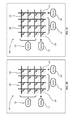
- FIG. 8A is a diagram of an example configuration for a three-dimensional bipolar memory cell array including a bidirectional access diode in accordance with one embodiment of the present invention.
- FIG. 8B is a diagram of an example configuration for a three-dimensional bipolar memory cell array including a bidirectional access diode in accordance with one embodiment of the present invention.
- FIG. 9 is a table of an optimized power supply scheme for a bipolar memory cell including a bidirectional access diode in accordance with one embodiment of the present invention.
- FIG. 10 is a flowchart illustrating an example method of operating a row switch for a bipolar memory cell array including a bidirectional access diode in accordance with one embodiment of the present invention.
- FIG. 11 is a flowchart illustrating an example method of operating a column switch for a bipolar memory cell array including a bidirectional access diode in accordance with one embodiment of the present invention.
- FIGS. 1A through 11 When referring to the figures, like structures and elements shown throughout are indicated with like reference numerals.
- Embodiments of the present invention provide possible systems for operating a bipolar memory cell with a bidirectional access diode, and possible methods for selecting from a plurality of bias voltages in such a system.
- the present invention is applicable to any three-dimensional memory array including bidirectional write operations.
- An aspect of the present invention provides a multistage decoding scheme for a bidirectional diode bipolar memory cell.
- Embodiments of the present invention provide that the first stage decoding scheme elements be directly coupled to the bidirectional access diode.
- the second stage decoding scheme elements and other circuitry can be shared by a plurality of first stage decoding scheme elements.
- the bias voltages can be from an external source or on-chip voltage generation circuitry. Such a mechanism is advantageous in providing efficient voltage selection in high-density memory arrays.
- the row lines in the diagrams represent bit lines in a memory cell array
- the column lines in the diagram represent word lines in a memory cell array.
- word and bit lines are interchangeable in alternate embodiments of the present invention.
- FIGS. 1A through 1C display three diagrams of an example bipolar memory cell array 100 including bidirectional access diodes in accordance with one embodiment of the present invention.
- bias conditions are used to select and deselect the word lines and bit lines.
- only positive bias voltages are utilized.
- the memory array 100 includes a memory cell in a select state 102 , memory cells in a select row 104 , memory cells in a select column 106 , and memory cells in a deselect state 108 .
- FIG. 1A is a diagram of the example bipolar memory cell array 100 during a write-zero state.
- the memory cells in a select row 104 and the memory cell in a select state 102 are coupled to a select write-zero row voltage 110 .
- the memory cells in a select column 106 and the memory cell in a select state 102 are coupled to a select write-zero column voltage 112 .
- the memory cells in a deselect state 108 and the memory cells in a select row 104 are coupled to a deselect write-zero column voltage 114 .
- the memory cells in a deselect state 108 and the memory cells in a select column 106 are coupled to a deselect write-zero row voltage 116 .
- FIG. 1B is a diagram of the example bipolar memory cell array 100 during a write-one state.
- the memory cells in a select row 104 and the memory cell in a select state 102 are coupled to a select write-one row voltage 120 .
- the memory cells in a select column 106 and the memory cell in a select state 102 are coupled to a select write-one column voltage 122 .
- the memory cells in a deselect state 108 and the memory cells in a select row 104 are coupled to a deselect write-one column voltage 124 .
- the memory cells in a deselect state 108 and the memory cells in a select column 106 are coupled to a deselect write-one row voltage 126 .
- FIG. 1C is a diagram of the example bipolar memory cell array 100 during a read state.
- the memory cells in a select row 104 and the memory cell in a select state 102 are coupled to a select read row voltage 130 .
- the memory cells in a select column 106 and the memory cell in a select state 102 are coupled to a select read column voltage 132 .
- the memory cells in a deselect state 108 and the memory cells in a select row 104 are coupled to a deselect read column voltage 134 .
- the memory cells in a deselect state 108 and the memory cells in a select column 106 are coupled to a deselect read row voltage 136 .
- FIGS. 2A through 2C display three diagrams of an example bipolar memory cell array 200 including bidirectional access diodes in accordance with one embodiment of the present invention.
- a single bias condition is used to select and deselect the word lines and bit lines.
- positive and negative bias voltages are utilized.
- the memory array 200 includes a memory cell in a select state 202 , a plurality of memory cells in a select row 204 , a plurality of memory cells in a select column 206 , and a plurality of memory cells in a deselect state 208 .
- FIG. 2A is a diagram of an example bipolar memory cell array 200 during a read state.
- the memory cells in a select row 204 and the memory cell in a select state 202 are coupled to a select read row voltage 210 .
- the memory cells in a select column 206 and the memory cell in a select state 202 are coupled to a select read column voltage 212 .
- the memory cells in a deselect state 208 and the memory cells in a select row 204 are coupled to a deselect read column voltage 214 .
- the memory cells in a deselect state 208 and the memory cells in a select column 206 are coupled to a deselect read row voltage 216 .
- FIG. 2B is a diagram of the example bipolar memory cell array 200 during a write-zero state.
- the memory cells in a select row 204 and the memory cell in a select state 202 are coupled to a select write-zero row voltage 220 .
- the memory cells in a select column 206 and the memory cell in a select state 202 are coupled to a select write-zero column voltage 222 .
- the memory cells in a deselect state 208 and the memory cells in a select row 204 are coupled to a deselect write-zero column voltage 224 .
- the memory cells in a deselect state 208 and the memory cells in a select column 206 are coupled to a deselect write-zero row voltage 226 .
- FIG. 2C is a diagram of the example bipolar memory cell array 200 during a write-one state.
- the memory cells in a select row 204 and the memory cell in a select state 202 are coupled to a select write-one row voltage 230 .
- the memory cells in a select column 206 and the memory cell in a select state 202 are coupled to a select write-one column voltage 232 .
- the memory cells in a deselect state 208 and the memory cells in a select row 204 are coupled to a deselect write-one column voltage 234 .
- the memory cells in a deselect state 208 and the memory cells in a select column 206 are coupled to a deselect write-one row voltage 236 .
- FIG. 3 is a diagram of an example system for operating a bipolar memory cell including a bidirectional access diode in accordance with one embodiment of the present invention.
- the system includes a decoding circuit 300 , the decoding circuit 300 includes a row voltage switch 302 .
- the row voltage switch 302 includes an output electrically coupled to the bidirectional access diode 301 .
- the bidirectional access diode includes a threshold voltage (V T ).
- the row voltage switch 302 includes a first stage row multiplexer 304 , wherein an output of the first stage row multiplexer 304 is electrically coupled to the bipolar memory cell 301 .
- the row voltage switch 302 also includes a second stage row switch 306 .
- the second stage row switch 306 includes a second stage select row multiplexer 308 , wherein an output of the second stage select row multiplexer 308 is electrically coupled to the first stage row multiplexer 304 .
- the second stage row switch 306 also includes a second stage deselect row multiplexer 310 , wherein an output of the second stage deselect row multiplexer 310 is electrically coupled to the first stage row multiplexer 304 .
- the row voltage switch 302 includes a third stage row switch 312 .
- the third stage row voltage switch 312 includes a select read row voltage 314 electrically coupled to the second stage select row multiplexer 308 .
- the third stage row voltage switch 312 includes a third stage select row multiplexer 316 including an output electrically coupled to the second stage select row multiplexer 308 .
- the third stage select row multiplexer 316 is also electrically coupled to a select write-one row voltage 318 (V W ) and a select write-zero row voltage 320 .
- the select write-zero row voltage 320 is a ground voltage (G).
- the third stage row switch 312 includes a deselect read row voltage 322 electrically coupled to the second stage deselect row multiplexer 310 .
- the deselect read row voltage 322 is equal to one half the difference between the select read row voltage 314 and the threshold voltage (V T ).
- the third stage row switch 312 also includes a third stage deselect row multiplexer 324 including an output electrically coupled to the second stage deselect row multiplexer 310 .
- the third stage deselect row multiplexer 324 is also electrically coupled to a deselect write-one row voltage 326 and a deselect write-zero row voltage 328 .
- the deselect write-one row voltage 326 is equal to one half the difference between the select write-zero row voltage 320 and the threshold voltage (V T ).
- the deselect write-zero row voltage 328 is equal to one half the sum of the select write-zero row voltage 320 and the threshold voltage (V T ).
- the decoding circuit 300 also includes a column voltage switch 332 .
- the column voltage switch 332 includes an output electrically coupled to the bidirectional access diode 301 .
- the column voltage switch 332 includes a first stage column multiplexer 334 , wherein an output of the first stage column multiplexer 334 is electrically coupled to the bipolar memory cell 301 .
- the column voltage switch 332 also includes a second stage column switch 336 .
- the second stage column switch 336 includes a second stage select column multiplexer 338 , wherein an output of the second stage select column multiplexer 338 is electrically coupled to the first stage column multiplexer 334 .
- the second stage column switch 336 also includes a second stage deselect column multiplexer 340 , wherein an output of the second stage deselect column multiplexer 340 is electrically coupled to the first stage column multiplexer 334 .
- the column voltage switch 332 includes a third stage column switch 342 .
- the third stage column voltage switch 342 includes a select read column voltage and a select write-one column voltage. In some embodiments the select read column voltage and the select write-one column voltage are equal. In this embodiment, the select read column voltage and select write-one column voltage are the same voltage supply, a select read/write-one column voltage 344 .
- the select read/write-one column voltage 344 is electrically coupled to the second stage select column multiplexer 338 .
- the select read/write-one column voltage 344 is a ground voltage (G).
- the third stage column voltage switch 342 includes a select write-zero column voltage 346 (V W ) electrically coupled to the second stage select column multiplexer 338 . In this embodiment, the select write-zero column voltage 346 is equal to the select write-one row voltage 318 .
- the third stage column switch 342 includes a deselect read column voltage 348 electrically coupled to the second stage deselect column multiplexer 340 .
- the deselect read column voltage 348 is equal to one half the sum of the select read row voltage 314 and the threshold voltage (V T ).
- the third stage column switch 342 also includes a third stage deselect column multiplexer 350 including an output electrically coupled to the second stage deselect column multiplexer 340 .
- the third stage deselect column multiplexer 350 is also electrically coupled to a deselect write-one column voltage 352 and a deselect write-zero column voltage 354 .
- the deselect write-one column voltage 352 is equal to one half the sum of the select write-one row voltage 318 and the threshold voltage (V T ).
- the deselect write-zero column voltage 354 is equal to one half the difference between the select write-one row voltage 318 and the threshold voltage (V T ).
- the decoding circuit 300 also includes a write driver 360 electrically coupled to a select line of the row voltage switch 302 and column voltage switch 332 .
- the decoding circuit also includes a row decoder 362 electrically coupled to a select line of the row voltage switch 302 .
- the decoding circuit also includes a column decoder 364 electrically coupled to a select line of the column voltage switch 332 .
- FIG. 4 is a diagram of an example system for operating a bipolar memory cell including a bidirectional access diode in accordance with one embodiment of the present invention.
- the system includes a decoding circuit 400 , the decoding circuit 400 includes a row voltage switch 402 .
- the row voltage switch includes a write-one row voltage 404 and a write-zero row voltage 406 .
- the decoding circuit 400 also includes a column voltage switch 410 .
- the column voltage switch includes a write-one column voltage 412 and a write-zero column voltage 414 .
- FIG. 5 is a diagram of an example system for operating a bipolar memory cell array including bidirectional access diodes in accordance with one embodiment of the present invention.
- the system includes a decoding circuit 500 , the decoding circuit 500 includes a plurality of first stage row/column multiplexers 502 .
- the decoding circuit 500 also includes a plurality of second stage row/column voltage switches 504 .
- the plurality of second stage row/column voltage switches 504 includes outputs electrically coupled to the plurality of first stage row/column multiplexers 502 .
- the decoding circuit 500 further includes a third stage row/column switch 506 including an output electrically coupled to the plurality of second stage row/column voltage switches 504 .
- the decoding circuit 500 includes a row/column decoder 508 electrically coupled to a select line in the plurality of first stage row/column multiplexers 502 .
- the second stage and third stage row/column voltage switches are shared between a plurality of first stage row/column multiplexers and memory storage elements.
- FIG. 6 is a diagram of an example configuration for a bipolar memory cell array including a bidirectional access diode in accordance with one embodiment of the present invention.
- the circuitry described in the embodiments above are located below the bit line, word line and memory storage elements.
- the horizontal bars represent the bit lines in the memory array.
- the cross bars represent the word lines in the memory array.
- the downward arrows between the word and bit lines represent the memory storage elements.
- the memory storage elements are integrated with the bidirectional access diode between two metal layers.
- the element below the array represents the decoding circuitry and local connections.
- FIG. 7 is a diagram of an example bipolar memory cell array including a bidirectional access diode in accordance with one embodiment of the present invention.
- the horizontal lines represent the bit lines in the memory array.
- the vertical lines represent the word lines in the memory array.
- the memory cells are represented by the diagonal arrows pointing to the lower right.
- a row driver and row decoder are electrically coupled to each bit line.
- a column driver, column decoder, sense amplifier and write head are electrically coupled to each word line.
- the four word lines on the right are arranged on top of the four word lines on the left, with the bit lines shared between them.
- FIG. 8A is a diagram of an example configuration for a bipolar memory cell array including a bidirectional access diode in accordance with one embodiment of the present invention.
- a column driver (M n ) is shared between a first memory cell 802 and a second memory cell 804 .
- the first memory cell 802 is coupled to a first row driver (M n+1 ).
- the second memory cell 804 is coupled to a second row driver (M n ⁇ 1 ).
- a row driver could take the place of the column driver, if a first and a second column driver could replace the row drivers.
- FIG. 8B is a diagram of another example configuration for a bipolar memory cell array including a bidirectional access diode in accordance with one embodiment of the present invention.
- two levels of memory cells are embedded between three metal layers.
- a shared word line (Shared WL) is shared between a first memory cell 812 and a second memory cell 814 .
- the first memory cell 812 is coupled to a first bit line (Upper BL).
- the second memory cell 814 is coupled to a second bit line (Lower BL).
- FIG. 9 is a table of an optimized power supply scheme for a bipolar memory cell including a bidirectional access diode in accordance with one embodiment of the present invention.
- V DD is equal to double V SBB
- V PP is equal to the sum of V SBB and V SBW .
- the number of supply voltages is minimized in this embodiment. Additionally, the voltage swing from a standby state to an active state is minimized in this embodiment.
- FIG. 10 is a flowchart illustrating an example method of operating a row switch for a bipolar memory cell array including a bidirectional access diode in accordance with one embodiment of the present invention. This method is described with reference to decoding circuit 300 . The method begins with determining step 1002 . At determining step 1002 , the operating state of the bipolar memory cell is determined as one of a select-state or a deselect-state.
- the method proceeds to switching step 1004 .
- the output signal of the first stage row multiplexer 304 is switched to a second stage select row multiplexer 308 .
- the method proceeds to determining step 1006 .
- the programming state of the bipolar memory cell is determined as one of a read-state or a write-state. If the programming state is one of a read-state, the method proceeds to switching step 1008 .
- the output signal of the second stage select row multiplexer 308 is switched to a select read row voltage 314 . After switching step 1008 , the method is complete.
- the method proceeds to switching step 1010 .
- the output signal of the second stage select row multiplexer 308 is switched to a third stage select row multiplexer 316 .
- the method proceeds to determining step 1012 .
- the binary state of the bipolar memory cell is determined as one of a write-zero state or a write-one state. If the binary state is one of a write-zero state, the method proceeds to switching step 1014 .
- the third stage select row multiplexer 316 is switched to a select write-zero row voltage 320 . After switching step 1014 , the method is complete.
- the method proceeds to switching step 1016 .
- the third stage select row multiplexer 316 is switched to a select write-one row voltage 318 .
- the method is complete.
- the method proceeds to switching step 1018 .
- the output signal of the first stage row multiplexer 304 is switched to a second stage deselect row multiplexer 310 .
- the method proceeds to determining step 1020 .
- the programming state of the bipolar memory cell is determined as one of a read-state or a write-state. If the programming state is one of a read-state, the method proceeds to switching step 1022 .
- the output signal of the second stage deselect row multiplexer 310 is switched to a deselect read row voltage 322 . After switching step 1022 , the method is complete.
- the method proceeds to switching step 1024 .
- the output signal of the second stage deselect row multiplexer 310 is switched to a third stage deselect row multiplexer 324 .
- the method proceeds to determining step 1026 .
- the binary state of the bipolar memory cell is determined as one of a write-zero state or a write-one state. If the binary state is one of a write-zero state, the method proceeds to switching step 1028 .
- the third stage deselect row multiplexer 324 is switched to a deselect write-zero row voltage 328 . After switching step 1028 , the method is complete.
- the method proceeds to switching step 1030 .
- the third stage deselect row multiplexer 324 is switched to a deselect write-one row voltage 326 . After switching step 1030 , the method is complete.
- FIG. 11 is a flowchart illustrating an example method of operating a column switch for a bipolar memory cell array including a bidirectional access diode in accordance with one embodiment of the present invention. This method is described with reference to decoding circuit 300 . The method begins with determining step 1102 . At determining step 1102 , the operating state of the bipolar memory cell is determined as one of a select-state or a deselect-state.
- the method proceeds to switching step 1104 .
- the output signal of the first stage column multiplexer 334 is switched to a second stage select column multiplexer 338 .
- the method proceeds to determining step 1106 .
- the programming state of the bipolar memory cell is determined as one of a read-state or a write-state. If the programming state is one of a read-state, the method proceeds to switching step 1108 .
- the output signal of the second stage select column multiplexer 338 is switched to a select read/write-one column voltage 344 . After switching step 1108 , the method is complete.
- the method proceeds to determining step 1112 .
- the binary state of the bipolar memory cell is determined as one of a write-zero state or a write-one state. If the binary state is one of a write-zero state, the method proceeds to switching step 1114 .
- the second stage select column multiplexer 338 is switched to a select write-zero column voltage 346 . After switching step 1114 , the method is complete.
- the method proceeds to switching step 1108 .
- the output signal of the second stage select column multiplexer 338 is switched to a select read/write-one column voltage 344 .
- the method is complete.
- the method proceeds to switching step 1118 .
- the output signal of the first stage column multiplexer 334 is switched to a second stage deselect column multiplexer 340 .
- the method proceeds to determining step 1120 .
- the programming state of the bipolar memory cell is determined as one of a read-state or a write-state. If the programming state is one of a read-state, the method proceeds to switching step 1122 .
- the output signal of the second stage deselect column multiplexer 340 is switched to a deselect read column voltage 348 . After switching step 1122 , the method is complete.
- the method proceeds to switching step 1124 .
- the output signal of the second stage deselect column multiplexer 340 is switched to a third stage deselect column multiplexer 350 .
- the method proceeds to determining step 1126 .
- the binary state of the bipolar memory cell is determined as one of a write-zero state or a write-one state. If the binary state is one of a write-zero state, the method proceeds to switching step 1128 .
- the third stage deselect column multiplexer 350 is switched to a deselect write-zero column voltage 354 . After switching step 1128 , the method is complete.
- the method proceeds to switching step 1130 .
- the third stage deselect column multiplexer 350 is switched to a deselect write-one column voltage 352 .
- the method is complete.
Landscapes
- Engineering & Computer Science (AREA)
- Microelectronics & Electronic Packaging (AREA)
- Chemical & Material Sciences (AREA)
- Crystallography & Structural Chemistry (AREA)
- Materials Engineering (AREA)
- Semiconductor Memories (AREA)
Abstract
Description
Claims (21)
Priority Applications (1)
| Application Number | Priority Date | Filing Date | Title |
|---|---|---|---|
| US13/407,848 US8755213B2 (en) | 2012-02-29 | 2012-02-29 | Decoding scheme for bipolar-based diode three-dimensional memory requiring bipolar programming |
Applications Claiming Priority (1)
| Application Number | Priority Date | Filing Date | Title |
|---|---|---|---|
| US13/407,848 US8755213B2 (en) | 2012-02-29 | 2012-02-29 | Decoding scheme for bipolar-based diode three-dimensional memory requiring bipolar programming |
Publications (2)
| Publication Number | Publication Date |
|---|---|
| US20130223125A1 US20130223125A1 (en) | 2013-08-29 |
| US8755213B2 true US8755213B2 (en) | 2014-06-17 |
Family
ID=49002699
Family Applications (1)
| Application Number | Title | Priority Date | Filing Date |
|---|---|---|---|
| US13/407,848 Expired - Fee Related US8755213B2 (en) | 2012-02-29 | 2012-02-29 | Decoding scheme for bipolar-based diode three-dimensional memory requiring bipolar programming |
Country Status (1)
| Country | Link |
|---|---|
| US (1) | US8755213B2 (en) |
Families Citing this family (6)
| Publication number | Priority date | Publication date | Assignee | Title |
|---|---|---|---|---|
| US9853053B2 (en) | 2012-09-10 | 2017-12-26 | 3B Technologies, Inc. | Three dimension integrated circuits employing thin film transistors |
| US8952470B2 (en) | 2012-09-10 | 2015-02-10 | James John Lupino | Low cost high density nonvolatile memory array device employing thin film transistors and back to back Schottky diodes |
| CN107112049A (en) | 2014-12-23 | 2017-08-29 | 3B技术公司 | Using the three dimensional integrated circuits of thin film transistor (TFT) |
| US9858975B1 (en) * | 2016-08-24 | 2018-01-02 | Samsung Electronics Co., Ltd. | Zero transistor transverse current bi-directional bitcell |
| JP2019040646A (en) * | 2017-08-22 | 2019-03-14 | 東芝メモリ株式会社 | Semiconductor storage device |
| US10790002B2 (en) | 2018-06-21 | 2020-09-29 | Samsung Electronics Co., Ltd. | Giant spin hall-based compact neuromorphic cell optimized for differential read inference |
Citations (11)
| Publication number | Priority date | Publication date | Assignee | Title |
|---|---|---|---|---|
| US4617653A (en) | 1982-12-29 | 1986-10-14 | Fujitsu Limited | Semiconductor memory device utilizing multi-stage decoding |
| US4660178A (en) | 1983-09-21 | 1987-04-21 | Inmos Corporation | Multistage decoding |
| US7382647B1 (en) | 2007-02-27 | 2008-06-03 | International Business Machines Corporation | Rectifying element for a crosspoint based memory array architecture |
| US20080151602A1 (en) * | 2006-12-25 | 2008-06-26 | Semiconductor Energy Laboratory Co., Ltd. | Nonvolatile memory and semiconductor device including nonvolatile memory |
| US7436698B2 (en) | 2004-04-27 | 2008-10-14 | Taiwan Semiconductor Manufacturing Co., Ltd. | MRAM arrays and methods for writing and reading magnetic memory devices |
| US7573736B2 (en) | 2007-05-22 | 2009-08-11 | Taiwan Semiconductor Manufacturing Company | Spin torque transfer MRAM device |
| US7646626B2 (en) * | 2006-04-27 | 2010-01-12 | Ovonyx, Inc. | Page mode access for non-volatile memory arrays |
| US20100085830A1 (en) | 2008-10-07 | 2010-04-08 | Shepard Daniel R | Sequencing Decoder Circuit |
| US20100118590A1 (en) | 2008-11-07 | 2010-05-13 | Seagate Technology Llc | Bidirectional Non-Volatile Memory Array Architecture |
| US7729163B2 (en) | 2008-03-26 | 2010-06-01 | Micron Technology, Inc. | Phase change memory |
| US7782661B2 (en) | 2007-04-24 | 2010-08-24 | Magic Technologies, Inc. | Boosted gate voltage programming for spin-torque MRAM array |
-
2012
- 2012-02-29 US US13/407,848 patent/US8755213B2/en not_active Expired - Fee Related
Patent Citations (11)
| Publication number | Priority date | Publication date | Assignee | Title |
|---|---|---|---|---|
| US4617653A (en) | 1982-12-29 | 1986-10-14 | Fujitsu Limited | Semiconductor memory device utilizing multi-stage decoding |
| US4660178A (en) | 1983-09-21 | 1987-04-21 | Inmos Corporation | Multistage decoding |
| US7436698B2 (en) | 2004-04-27 | 2008-10-14 | Taiwan Semiconductor Manufacturing Co., Ltd. | MRAM arrays and methods for writing and reading magnetic memory devices |
| US7646626B2 (en) * | 2006-04-27 | 2010-01-12 | Ovonyx, Inc. | Page mode access for non-volatile memory arrays |
| US20080151602A1 (en) * | 2006-12-25 | 2008-06-26 | Semiconductor Energy Laboratory Co., Ltd. | Nonvolatile memory and semiconductor device including nonvolatile memory |
| US7382647B1 (en) | 2007-02-27 | 2008-06-03 | International Business Machines Corporation | Rectifying element for a crosspoint based memory array architecture |
| US7782661B2 (en) | 2007-04-24 | 2010-08-24 | Magic Technologies, Inc. | Boosted gate voltage programming for spin-torque MRAM array |
| US7573736B2 (en) | 2007-05-22 | 2009-08-11 | Taiwan Semiconductor Manufacturing Company | Spin torque transfer MRAM device |
| US7729163B2 (en) | 2008-03-26 | 2010-06-01 | Micron Technology, Inc. | Phase change memory |
| US20100085830A1 (en) | 2008-10-07 | 2010-04-08 | Shepard Daniel R | Sequencing Decoder Circuit |
| US20100118590A1 (en) | 2008-11-07 | 2010-05-13 | Seagate Technology Llc | Bidirectional Non-Volatile Memory Array Architecture |
Non-Patent Citations (1)
| Title |
|---|
| G. W. Burr et al., review the capabilities of ferroelectric, magnetic, phase-change, and resistive random-access memories, including perovskites and solid electrolytes, and finally organic and polymeric memory, IBM J. Res. & Dev. vol. 52 No. 4/5, pp. 449-464 (2008 ). |
Also Published As
| Publication number | Publication date |
|---|---|
| US20130223125A1 (en) | 2013-08-29 |
Similar Documents
| Publication | Publication Date | Title |
|---|---|---|
| JP5032621B2 (en) | Nonvolatile semiconductor memory and manufacturing method thereof | |
| JP5396011B2 (en) | Phase change memory device | |
| JP4445398B2 (en) | Phase change memory device | |
| US8508975B2 (en) | Resistive storage-based semiconductor memory device | |
| US8755213B2 (en) | Decoding scheme for bipolar-based diode three-dimensional memory requiring bipolar programming | |
| US9508427B2 (en) | Apparatuses and methods including supply current in memory | |
| US8139404B2 (en) | Semiconductor memory device | |
| JP2016167332A (en) | Storage device | |
| US9153625B2 (en) | Non-volatile semiconductor memory device | |
| JP2013200929A (en) | Semiconductor memory | |
| US6778434B2 (en) | Magnetic random access memory device with a reduced number of interconnections for selection of address | |
| US8873271B2 (en) | 3D architecture for bipolar memory using bipolar access device | |
| US7869267B2 (en) | Method for low power accessing a phase change memory device | |
| JP2011060389A (en) | Semiconductor memory device | |
| US10468081B2 (en) | Semiconductor storage device | |
| KR20090090602A (en) | Phase-change random access memory capable of reducing noise on wordline | |
| JP2009252283A (en) | Semiconductor memory device | |
| US20160055895A1 (en) | Semiconductor storage device | |
| US8842491B2 (en) | Decoding scheme for bipolar-based diode three-dimensional memory requiring unipolar programming | |
| US7590012B2 (en) | Semiconductor storage device | |
| US11049549B2 (en) | Decoder structure including array of decoder cells organized into different rows | |
| US20220302214A1 (en) | Semiconductor storage device | |
| US9478283B2 (en) | Nonvolatile semiconductor storage device having improved reading and writing speed characteristics | |
| KR20090097723A (en) | Phase change random access memory and layout method of the same |
Legal Events
| Date | Code | Title | Description |
|---|---|---|---|
| AS | Assignment |
Owner name: INTERNATIONAL BUSINESS MACHINES CORPORATION, NEW Y Free format text: ASSIGNMENT OF ASSIGNORS INTEREST;ASSIGNORS:DEBROSSE, JOHN K.;GOPALAKRISHNAN, KAILASH;LAM, CHUNG H.;AND OTHERS;SIGNING DATES FROM 20120210 TO 20120217;REEL/FRAME:027785/0665 |
|
| AS | Assignment |
Owner name: GLOBALFOUNDRIES U.S. 2 LLC, NEW YORK Free format text: ASSIGNMENT OF ASSIGNORS INTEREST;ASSIGNOR:INTERNATIONAL BUSINESS MACHINES CORPORATION;REEL/FRAME:036550/0001 Effective date: 20150629 |
|
| AS | Assignment |
Owner name: GLOBALFOUNDRIES INC., CAYMAN ISLANDS Free format text: ASSIGNMENT OF ASSIGNORS INTEREST;ASSIGNORS:GLOBALFOUNDRIES U.S. 2 LLC;GLOBALFOUNDRIES U.S. INC.;REEL/FRAME:036779/0001 Effective date: 20150910 |
|
| FEPP | Fee payment procedure |
Free format text: MAINTENANCE FEE REMINDER MAILED (ORIGINAL EVENT CODE: REM.) |
|
| LAPS | Lapse for failure to pay maintenance fees |
Free format text: PATENT EXPIRED FOR FAILURE TO PAY MAINTENANCE FEES (ORIGINAL EVENT CODE: EXP.) |
|
| STCH | Information on status: patent discontinuation |
Free format text: PATENT EXPIRED DUE TO NONPAYMENT OF MAINTENANCE FEES UNDER 37 CFR 1.362 |
|
| FP | Lapsed due to failure to pay maintenance fee |
Effective date: 20180617 |
|
| FP | Lapsed due to failure to pay maintenance fee |
Effective date: 20180617 |
|
| AS | Assignment |
Owner name: GLOBALFOUNDRIES U.S. INC., NEW YORK Free format text: RELEASE BY SECURED PARTY;ASSIGNOR:WILMINGTON TRUST, NATIONAL ASSOCIATION;REEL/FRAME:056987/0001 Effective date: 20201117 |