JP5288479B2 - 表示パネルドライバ - Google Patents
表示パネルドライバ Download PDFInfo
- Publication number
- JP5288479B2 JP5288479B2 JP2009108404A JP2009108404A JP5288479B2 JP 5288479 B2 JP5288479 B2 JP 5288479B2 JP 2009108404 A JP2009108404 A JP 2009108404A JP 2009108404 A JP2009108404 A JP 2009108404A JP 5288479 B2 JP5288479 B2 JP 5288479B2
- Authority
- JP
- Japan
- Prior art keywords
- output
- switch
- amplifier
- electrostatic protection
- odd
- Prior art date
- Legal status (The legal status is an assumption and is not a legal conclusion. Google has not performed a legal analysis and makes no representation as to the accuracy of the status listed.)
- Active
Links
Images


Classifications
-
- G—PHYSICS
- G09—EDUCATION; CRYPTOGRAPHY; DISPLAY; ADVERTISING; SEALS
- G09G—ARRANGEMENTS OR CIRCUITS FOR CONTROL OF INDICATING DEVICES USING STATIC MEANS TO PRESENT VARIABLE INFORMATION
- G09G3/00—Control arrangements or circuits, of interest only in connection with visual indicators other than cathode-ray tubes
- G09G3/20—Control arrangements or circuits, of interest only in connection with visual indicators other than cathode-ray tubes for presentation of an assembly of a number of characters, e.g. a page, by composing the assembly by combination of individual elements arranged in a matrix no fixed position being assigned to or needed to be assigned to the individual characters or partial characters
- G09G3/34—Control arrangements or circuits, of interest only in connection with visual indicators other than cathode-ray tubes for presentation of an assembly of a number of characters, e.g. a page, by composing the assembly by combination of individual elements arranged in a matrix no fixed position being assigned to or needed to be assigned to the individual characters or partial characters by control of light from an independent source
- G09G3/36—Control arrangements or circuits, of interest only in connection with visual indicators other than cathode-ray tubes for presentation of an assembly of a number of characters, e.g. a page, by composing the assembly by combination of individual elements arranged in a matrix no fixed position being assigned to or needed to be assigned to the individual characters or partial characters by control of light from an independent source using liquid crystals
- G09G3/3611—Control of matrices with row and column drivers
- G09G3/3685—Details of drivers for data electrodes
- G09G3/3688—Details of drivers for data electrodes suitable for active matrices only
-
- G—PHYSICS
- G09—EDUCATION; CRYPTOGRAPHY; DISPLAY; ADVERTISING; SEALS
- G09G—ARRANGEMENTS OR CIRCUITS FOR CONTROL OF INDICATING DEVICES USING STATIC MEANS TO PRESENT VARIABLE INFORMATION
- G09G2320/00—Control of display operating conditions
- G09G2320/02—Improving the quality of display appearance
- G09G2320/0223—Compensation for problems related to R-C delay and attenuation in electrodes of matrix panels, e.g. in gate electrodes or on-substrate video signal electrodes
-
- G—PHYSICS
- G09—EDUCATION; CRYPTOGRAPHY; DISPLAY; ADVERTISING; SEALS
- G09G—ARRANGEMENTS OR CIRCUITS FOR CONTROL OF INDICATING DEVICES USING STATIC MEANS TO PRESENT VARIABLE INFORMATION
- G09G2330/00—Aspects of power supply; Aspects of display protection and defect management
- G09G2330/04—Display protection
-
- G—PHYSICS
- G09—EDUCATION; CRYPTOGRAPHY; DISPLAY; ADVERTISING; SEALS
- G09G—ARRANGEMENTS OR CIRCUITS FOR CONTROL OF INDICATING DEVICES USING STATIC MEANS TO PRESENT VARIABLE INFORMATION
- G09G3/00—Control arrangements or circuits, of interest only in connection with visual indicators other than cathode-ray tubes
- G09G3/20—Control arrangements or circuits, of interest only in connection with visual indicators other than cathode-ray tubes for presentation of an assembly of a number of characters, e.g. a page, by composing the assembly by combination of individual elements arranged in a matrix no fixed position being assigned to or needed to be assigned to the individual characters or partial characters
- G09G3/34—Control arrangements or circuits, of interest only in connection with visual indicators other than cathode-ray tubes for presentation of an assembly of a number of characters, e.g. a page, by composing the assembly by combination of individual elements arranged in a matrix no fixed position being assigned to or needed to be assigned to the individual characters or partial characters by control of light from an independent source
- G09G3/36—Control arrangements or circuits, of interest only in connection with visual indicators other than cathode-ray tubes for presentation of an assembly of a number of characters, e.g. a page, by composing the assembly by combination of individual elements arranged in a matrix no fixed position being assigned to or needed to be assigned to the individual characters or partial characters by control of light from an independent source using liquid crystals
- G09G3/3611—Control of matrices with row and column drivers
- G09G3/3614—Control of polarity reversal in general
-
- H—ELECTRICITY
- H01—ELECTRIC ELEMENTS
- H01L—SEMICONDUCTOR DEVICES NOT COVERED BY CLASS H10
- H01L2924/00—Indexing scheme for arrangements or methods for connecting or disconnecting semiconductor or solid-state bodies as covered by H01L24/00
- H01L2924/0001—Technical content checked by a classifier
- H01L2924/0002—Not covered by any one of groups H01L24/00, H01L24/00 and H01L2224/00
Description
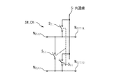
図4は、本発明の第1の実施形態のLCDドライバの出力回路の構成を示す回路図である。第1の実施形態の出力回路は、負側アンプ1と、正側アンプ2と、偶数出力パッド3と、奇数出力パッド4と、静電保護抵抗RESD1G、RESD2G、RESD1K、RESD2Kとを備えている。偶数出力パッド3と奇数出力パッド4とは、LCDパネルのデータ線に接続されるパットである。負側アンプ1は、“負極性”の駆動電圧を生成する演算増幅器であり、正側アンプ2は、“正極性”の駆動電圧を生成する演算増幅器である。ここで、本明細書において“正極性”とは、LCDパネルの対向電極に供給される共通電圧より高いことを意味し、逆に、“負極性”とは、当該共通電圧より低いことを意味することに留意されたい。負側アンプ1と正側アンプ2それぞれの正転入力端子は、それぞれ、各々負側D/Aコンバータ(Digital to Analog Converter)と正側D/Aコンバータに接続される。負側D/Aコンバータは、画像データに応じて“負極性”の階調電圧を負側アンプ1の正転入力端子に供給し、正側D/Aコンバータは、LCDドライバに供給された画像データに応じて“正極性”の階調電圧を正側アンプ2の正転入力端子に供給する。負側アンプ1と正側アンプ2のそれぞれは、ボルテッジフォロワ接続されており、供給された階調電圧と同一の駆動電圧を出力する。負側アンプ1によって生成された“負極性”の駆動電圧は、偶数出力パッド3と奇数出力パッド4の一方に供給され、正側アンプ2によって生成された“正極性”の駆動電圧は、偶数出力パッド3と奇数出力パッド4の他方に供給される。また、静電保護抵抗RESD1Gは、出力ノードNOUT1Gと偶数出力パッド3の間に接続され、静電保護抵抗RESD2Gは、出力ノードNOUT2Gと偶数出力パッド3の間に接続されている。また、静電保護抵抗RESD1Kは、出力ノードNOUT1Kと奇数出力パッド4の間に接続され、静電保護抵抗RESD2Kは、出力ノードNOUT2Kと奇数出力パッド4の間に接続されている。
図6Aは、第2の実施形態の出力回路の構成を示すブロック図である。図6Aの回路構成は図4の回路構成を一般化したもので、第2の実施形態の出力回路では、負側アンプ1と出力パッド(偶数出力パッド3又は奇数出力パッド4)とを接続する経路がn個設けられ、同様に、正側アンプ2と出力パッド(偶数出力パッド3又は奇数出力パッド4)とを接続する経路がn個設けられる。図4の回路構成は、図6Aの回路構成においてnを2とした場合の例である。
図7Aは、第3の実施形態における出力回路の構成を示すブロック図である。図7Aの回路では、図6Aの回路における負側アンプ1及び正側アンプ2が、Rail-to-Rail構成のアンプ1A、2Aに置き換えられている。これに伴い、アンプ1A及び2Aと正側D/Aコンバータ及び負側D/Aコンバータとの間にクロススイッチブロック6が挿入され、更に、極性切換スイッチブロックSW_POL1〜SW_POLnが、ストレートスイッチブロックSW_ST1〜SW_STnに置換される。クロススイッチブロック6は、スイッチSST1、SST2、SCR1、SCR2を備えている。スイッチSST1は、負側D/Aコンバータの出力とアンプ1Aの正転入力端子の間に接続され、スイッチSST2は、正側D/Aコンバータの出力とアンプ2Aの正転入力端子の間に接続される。また、スイッチSCR1は、負側D/Aコンバータの出力とアンプ2Aの正転入力端子の間に接続され、スイッチSCR2は、正側D/Aコンバータの出力とアンプ1Aの正転入力端子の間に接続される。
上述の第1〜第3の実施形態の出力回路におけるスイッチとしては、様々なものが使用され得る。スイッチとして、NMOSトランジスタが使用されてもよく、PMOSトランジスタが使用されてもよい。また、図8に図示されているような、ドレインとソースが共通に接続された一対のNMOSトランジスタ11及びPMOSトランジスタ12で構成されたトランスファーゲートが使用されてもよい。この場合、NMOSトランジスタ11及びPMOSトランジスタ12のゲートにはインバータ13を用いて互いに相補の制御信号が供給される。これにより、NMOSトランジスタ11及びPMOSトランジスタ12は同時にオン状態になり、又は同時にオフ状態になる。
2:正側アンプ
1A、2A:アンプ
3:偶数出力パッド
4:奇数出力パッド
5:共通線
6:クロススイッチブロック
11:NMOSトランジスタ
12:PMOSトランジスタ
13:インバータ
101:負側アンプ
102:正側アンプ
103:偶数出力パッド
104:奇数出力パッド
105:共通線
106:内部回路
107:出力端子パッド
108:インバータ
Claims (1)
- 第1及び第2アンプと、
第1〜第n偶数出力ノードと(nは、2以上の整数)、
第1〜第n奇数出力ノードと、
表示パネルのデータ線にそれぞれに接続される第1及び第2出力パッドと、
第1〜第nスイッチブロックと、
第1〜第n偶数静電保護抵抗と、
第1〜第n奇数静電保護抵抗
とを具備し、
前記第1〜第nスイッチブロックのうちの第iスイッチブロックは、前記第1及び第2アンプと、前記第i偶数出力ノード及び前記第i奇数出力ノードとの間の接続関係を切り換えるように構成され、
前記第1〜第n偶数静電保護抵抗が、それぞれ、前記第1〜第n偶数出力ノードと前記第1出力パッドとの間に接続され、
前記第1〜第n奇数静電保護抵抗が、それぞれ、前記第1〜第n奇数出力ノードと前記第2出力パッドとの間に接続され、
前記第1アンプは、前記表示パネルの対向電極に供給される共通電圧より低い駆動電圧を生成するように構成され、
前記第2アンプは、前記共通電圧より高い駆動電圧を生成するように構成され、
前記第1〜第nスイッチブロックのうちの第iスイッチブロックは、
前記第1アンプと前記第i偶数出力ノードとの間に設けられた第1スイッチと、
前記第2アンプと前記第i奇数出力ノードとの間に設けられた第2スイッチと、
前記第1アンプと前記第i奇数出力ノードとの間に設けられた第3スイッチと、
前記第2アンプと前記第i偶数出力ノードとの間に設けられた第4スイッチ
とを備えている
表示パネルドライバ。
Priority Applications (3)
| Application Number | Priority Date | Filing Date | Title |
|---|---|---|---|
| JP2009108404A JP5288479B2 (ja) | 2009-04-27 | 2009-04-27 | 表示パネルドライバ |
| US12/662,627 US8570313B2 (en) | 2009-04-27 | 2010-04-26 | Display panel driver |
| CN201010170050.6A CN101930716B (zh) | 2009-04-27 | 2010-04-27 | 显示面板驱动器 |
Applications Claiming Priority (1)
| Application Number | Priority Date | Filing Date | Title |
|---|---|---|---|
| JP2009108404A JP5288479B2 (ja) | 2009-04-27 | 2009-04-27 | 表示パネルドライバ |
Publications (3)
| Publication Number | Publication Date |
|---|---|
| JP2010256734A JP2010256734A (ja) | 2010-11-11 |
| JP2010256734A5 JP2010256734A5 (ja) | 2012-04-05 |
| JP5288479B2 true JP5288479B2 (ja) | 2013-09-11 |
Family
ID=42991734
Family Applications (1)
| Application Number | Title | Priority Date | Filing Date |
|---|---|---|---|
| JP2009108404A Active JP5288479B2 (ja) | 2009-04-27 | 2009-04-27 | 表示パネルドライバ |
Country Status (3)
| Country | Link |
|---|---|
| US (1) | US8570313B2 (ja) |
| JP (1) | JP5288479B2 (ja) |
| CN (1) | CN101930716B (ja) |
Families Citing this family (3)
| Publication number | Priority date | Publication date | Assignee | Title |
|---|---|---|---|---|
| TWI530926B (zh) * | 2011-05-03 | 2016-04-21 | 天鈺科技股份有限公司 | 源極驅動器及顯示裝置 |
| SG10201609410PA (en) * | 2015-11-30 | 2017-06-29 | Semiconductor Energy Lab | Semiconductor device, display panel, and electronic device |
| US10083668B2 (en) * | 2016-03-09 | 2018-09-25 | Semiconductor Energy Laboratory Co., Ltd. | Semiconductor device, display device, and electronic device |
Family Cites Families (10)
| Publication number | Priority date | Publication date | Assignee | Title |
|---|---|---|---|---|
| US6392636B1 (en) * | 1998-01-22 | 2002-05-21 | Stmicroelectronics, Inc. | Touchpad providing screen cursor/pointer movement control |
| JP2000260948A (ja) * | 1999-03-12 | 2000-09-22 | Toshiba Corp | 半導体装置 |
| JP2001358300A (ja) * | 2000-06-12 | 2001-12-26 | Fujitsu Ltd | 半導体集積回路装置 |
| JP4744686B2 (ja) * | 2000-12-06 | 2011-08-10 | ルネサスエレクトロニクス株式会社 | 演算増幅器 |
| JP4200683B2 (ja) * | 2002-04-16 | 2008-12-24 | セイコーエプソン株式会社 | 駆動回路、電気光学パネル、及び電子機器 |
| JP4744851B2 (ja) * | 2004-11-12 | 2011-08-10 | ルネサスエレクトロニクス株式会社 | 駆動回路及び表示装置 |
| JP5027464B2 (ja) * | 2006-09-08 | 2012-09-19 | ローム株式会社 | 電源装置、液晶駆動装置、表示装置 |
| JP4275166B2 (ja) * | 2006-11-02 | 2009-06-10 | Necエレクトロニクス株式会社 | データドライバ及び表示装置 |
| KR101423197B1 (ko) * | 2006-12-11 | 2014-07-25 | 삼성디스플레이 주식회사 | 데이터 구동 장치 및 그것을 이용하는 액정 표시 장치 |
| JP5362469B2 (ja) * | 2009-02-26 | 2013-12-11 | ラピスセミコンダクタ株式会社 | 液晶パネルの駆動回路 |
-
2009
- 2009-04-27 JP JP2009108404A patent/JP5288479B2/ja active Active
-
2010
- 2010-04-26 US US12/662,627 patent/US8570313B2/en active Active
- 2010-04-27 CN CN201010170050.6A patent/CN101930716B/zh active Active
Also Published As
| Publication number | Publication date |
|---|---|
| CN101930716B (zh) | 2014-10-01 |
| CN101930716A (zh) | 2010-12-29 |
| JP2010256734A (ja) | 2010-11-11 |
| US20100271364A1 (en) | 2010-10-28 |
| US8570313B2 (en) | 2013-10-29 |
Similar Documents
| Publication | Publication Date | Title |
|---|---|---|
| JP5048081B2 (ja) | バッファおよび表示装置 | |
| JP4921106B2 (ja) | バッファ回路 | |
| JP5075051B2 (ja) | Ab級増幅回路、及び表示装置 | |
| CN108091307B (zh) | 输出电路以及液晶显示装置的数据驱动器 | |
| JP5074914B2 (ja) | 出力ドライバ回路 | |
| US7750687B2 (en) | Circuit arrangement comprising a level shifter and method | |
| JP5442558B2 (ja) | 出力回路及びデータドライバ及び表示装置 | |
| US8130217B2 (en) | Display panel driving apparatus | |
| KR20150000768A (ko) | 디스플레이 구동회로 및 디스플레이 장치 | |
| US11012074B1 (en) | Off chip driving circuit and signal compensation method | |
| US10756737B1 (en) | Off chip driver circuit, off chip driver compensation system and signal compensation method | |
| JP5288479B2 (ja) | 表示パネルドライバ | |
| US7564392B2 (en) | Decoder circuit | |
| US7449916B2 (en) | Voltage level shift circuit | |
| US11341881B2 (en) | Level shifter circuit applied to display apparatus | |
| US8692618B2 (en) | Positive and negative voltage input operational amplifier set | |
| US6812781B2 (en) | Differential amplifier, semiconductor device, power supply circuit and electronic equipment using the same | |
| JP5576248B2 (ja) | 電源スイッチ回路 | |
| US8193865B2 (en) | Output circuit using analog amplifier | |
| JP5021501B2 (ja) | 出力ドライバ回路 | |
| US7826275B2 (en) | Memory circuit with high reading speed and low switching noise | |
| CN111865278A (zh) | 输出级电路及其控制方法 | |
| JP2009188790A (ja) | 出力バッファ回路 | |
| JP4963489B2 (ja) | 駆動装置 | |
| KR20070070992A (ko) | 소형 티에프티 구동 드라이버 아이시 제품의디지털-아날로그 컨버터 |
Legal Events
| Date | Code | Title | Description |
|---|---|---|---|
| A521 | Written amendment |
Free format text: JAPANESE INTERMEDIATE CODE: A523 Effective date: 20120221 |
|
| A621 | Written request for application examination |
Free format text: JAPANESE INTERMEDIATE CODE: A621 Effective date: 20120221 |
|
| A977 | Report on retrieval |
Free format text: JAPANESE INTERMEDIATE CODE: A971007 Effective date: 20130213 |
|
| A131 | Notification of reasons for refusal |
Free format text: JAPANESE INTERMEDIATE CODE: A131 Effective date: 20130222 |
|
| A521 | Written amendment |
Free format text: JAPANESE INTERMEDIATE CODE: A523 Effective date: 20130423 |
|
| TRDD | Decision of grant or rejection written | ||
| A01 | Written decision to grant a patent or to grant a registration (utility model) |
Free format text: JAPANESE INTERMEDIATE CODE: A01 Effective date: 20130529 |
|
| A61 | First payment of annual fees (during grant procedure) |
Free format text: JAPANESE INTERMEDIATE CODE: A61 Effective date: 20130530 |
|
| R150 | Certificate of patent or registration of utility model |
Ref document number: 5288479 Country of ref document: JP Free format text: JAPANESE INTERMEDIATE CODE: R150 |
|
| S531 | Written request for registration of change of domicile |
Free format text: JAPANESE INTERMEDIATE CODE: R313531 |
|
| R350 | Written notification of registration of transfer |
Free format text: JAPANESE INTERMEDIATE CODE: R350 |