JP5286938B2 - Needle mark inspection device, probe device, needle mark inspection method, and storage medium - Google Patents
Needle mark inspection device, probe device, needle mark inspection method, and storage medium Download PDFInfo
- Publication number
- JP5286938B2 JP5286938B2 JP2008138353A JP2008138353A JP5286938B2 JP 5286938 B2 JP5286938 B2 JP 5286938B2 JP 2008138353 A JP2008138353 A JP 2008138353A JP 2008138353 A JP2008138353 A JP 2008138353A JP 5286938 B2 JP5286938 B2 JP 5286938B2
- Authority
- JP
- Japan
- Prior art keywords
- component
- electrode pad
- needle
- data
- image data
- Prior art date
- Legal status (The legal status is an assumption and is not a legal conclusion. Google has not performed a legal analysis and makes no representation as to the accuracy of the status listed.)
- Active
Links
Images


Classifications
-
- G—PHYSICS
- G01—MEASURING; TESTING
- G01N—INVESTIGATING OR ANALYSING MATERIALS BY DETERMINING THEIR CHEMICAL OR PHYSICAL PROPERTIES
- G01N21/00—Investigating or analysing materials by the use of optical means, i.e. using sub-millimetre waves, infrared, visible or ultraviolet light
- G01N21/84—Systems specially adapted for particular applications
- G01N21/88—Investigating the presence of flaws or contamination
- G01N21/95—Investigating the presence of flaws or contamination characterised by the material or shape of the object to be examined
- G01N21/956—Inspecting patterns on the surface of objects
- G01N21/95684—Patterns showing highly reflecting parts, e.g. metallic elements
-
- G—PHYSICS
- G01—MEASURING; TESTING
- G01N—INVESTIGATING OR ANALYSING MATERIALS BY DETERMINING THEIR CHEMICAL OR PHYSICAL PROPERTIES
- G01N21/00—Investigating or analysing materials by the use of optical means, i.e. using sub-millimetre waves, infrared, visible or ultraviolet light
- G01N21/84—Systems specially adapted for particular applications
- G01N21/88—Investigating the presence of flaws or contamination
- G01N21/8851—Scan or image signal processing specially adapted therefor, e.g. for scan signal adjustment, for detecting different kinds of defects, for compensating for structures, markings, edges
- G01N2021/8887—Scan or image signal processing specially adapted therefor, e.g. for scan signal adjustment, for detecting different kinds of defects, for compensating for structures, markings, edges based on image processing techniques
Description
本発明は、例えばプローブ針を用いて検査した後の基板について電極パッドの下地層の露出の有無等の露出状況を自動的に検出する針跡検査装置、及び針跡検査方法、並びに針跡検査装置を備えたプローブ装置と、針跡検査方法の実行プログラムが記憶された記憶媒体に関する。 The present invention relates to a needle trace inspection apparatus, a needle trace inspection method, and a needle trace inspection that automatically detect, for example, an exposure state such as whether or not an underlying layer of an electrode pad is exposed on a substrate after being inspected using a probe needle. The present invention relates to a probe device including the device and a storage medium in which an execution program of a needle trace inspection method is stored.
従来、半導体の基板上に形成されたICチップの電気的な特性を測定する装置としてプローブ装置が使用されている。プローブ装置は、基板を載置して3次元方向に自由に移動可能なステージと、プローブカードとを備えており、基板上の配線パターンに接続された電極パッドにプローブカードのプローブ針を接触させる、所謂プローブテストを行うことによってチップの電気的測定を行う装置である。 Conventionally, a probe device has been used as a device for measuring the electrical characteristics of an IC chip formed on a semiconductor substrate. The probe apparatus includes a stage on which a substrate is placed and can freely move in a three-dimensional direction, and a probe card, and a probe needle of the probe card is brought into contact with an electrode pad connected to a wiring pattern on the substrate. This is a device that performs electrical measurement of a chip by performing a so-called probe test.
プローブとしては一般的にプローブ針が使用され、電極パッドの表面の自然酸化膜を削り取るためにオーバドライブ(プローブ針と電極パッドとが接触してから更に電極パッドを上昇させること)をかけるようにしている。そしてプローブ針が横針の場合には、オーバドライブをかけたときにプローブ針が横滑りするために縦長の針跡が形成され、プローブ針が垂直針の場合でも、確実な接触を確保するために基板ステージを横に動かして縦長の針跡が形成されることもある。 As a probe, a probe needle is generally used, and overdrive (to raise the electrode pad further after the probe needle and the electrode pad come into contact with each other) is applied in order to scrape the natural oxide film on the surface of the electrode pad. ing. When the probe needle is a horizontal needle, the probe needle slides sideways when overdrive is applied, and a long needle mark is formed. Even when the probe needle is a vertical needle, to ensure a reliable contact A vertically long needle trace may be formed by moving the substrate stage horizontally.
従って、プローブテスト後に電極パッドの針跡を検出して電極パッド上に針跡が存在するか否かを把握し、針跡がない場合には測定不良と判断するようにしている。更にプローブ針が予定しているよりも深く電極パッドに突き刺さって電極パッドの下地層が露出した場合にはデバイスの信頼性が落ちるため、それらの電極パッドについては不良として取り扱う必要があり、またそのような深堀りが起きると下地層の削り滓がプローブ針に付着してコンタミの要因となる。従って針跡の検出においては、速やかに露出の有無を検出する必要がある。 Therefore, the needle trace on the electrode pad is detected after the probe test to determine whether or not the needle trace exists on the electrode pad. If there is no needle trace, it is determined that the measurement is defective. Furthermore, if the probe needle penetrates deeper than expected and the underlying layer of the electrode pad is exposed, the reliability of the device will be reduced, so these electrode pads must be treated as defective, and When such deep drilling occurs, the shavings of the underlayer adhere to the probe needle and cause contamination. Therefore, in detecting the needle trace, it is necessary to quickly detect the presence or absence of exposure.
上記電極パッドの針跡検査については基板がプローブ装置から搬出された後、当該基板に対して作業者が金属顕微鏡等を使用して行っている。しかしながら一枚の基板からは多数例えば1000個のチップが製造され、一つのチップには複数例えば10個の電極パッドが形成されることから、針跡検査を行う電極パッドの数は膨大な数になる。そのため従来の針跡検査作業では検査に非常に長い時間が掛かるし、また金属顕微鏡を用意する必要があった。 The electrode pad needle mark inspection is performed by an operator using a metal microscope or the like on the substrate after the substrate is unloaded from the probe device. However, a large number of, for example, 1000 chips are manufactured from one substrate, and a plurality of, for example, 10 electrode pads are formed on one chip. Therefore, the number of electrode pads for needle trace inspection is enormous. Become. Therefore, in the conventional needle trace inspection work, the inspection takes a very long time, and it is necessary to prepare a metal microscope.
このような問題に対し、CCDカメラ等によってウェハWを撮像し、その撮像データを制御部にて解析して針跡検査を行う針跡検査装置がある。例えば特許文献1には、プローブテスト後の基板を撮像し、半導体チップにおけるプローブ針の接触痕を2次元画像として取得してこの2次元画像を解析して針跡を検出すると共に、針跡における色の濃度値の平均値を調べ、この平均値と、予め定められた平均値に対応する穴の深さを備えたデータをと比較することによって、針跡の深さを判定することが可能な針跡検出測定装置が記載されている。
In order to solve such a problem, there is a needle trace inspection apparatus that images a wafer W with a CCD camera or the like and analyzes the captured data by a control unit to perform a needle trace inspection. For example, in
また特許文献2には、基板を撮像して基板上面の画像データを取得し、画像データから電極パッド領域のデータを取得して針痕閾値決定部によって電極パッド領域の画素値のヒストグラムを求めると共に、ヒストグラムから針痕領域取得用の閾値を求め、この閾値を基に電極パッド領域を二値化して針跡の位置を正確に検出する針跡検出装置が記載されている。また特許文献3には、基板を撮像して基板上面の画像データを取得し、画像データから電極パッド領域のデータを取得して針痕閾値決定部によって電極パッド領域の画素値のヒストグラムを求めると共に針痕領域取得用の閾値を求め、電極パッド領域を複数の領域に分割して、領域ごとに求めた閾値を基に個別の閾値を設定して針跡を正確に検出する針跡検出装置が記載されている。
In
しかしながら上述した各装置では、撮像手段としてモノクロカメラを使用するため、例えば図22に示すように、基板を撮像すると電極パッド100のデータがモノクロ画像として取得される。このとき電極パッド100の中央に楕円形の針跡110が形成され、その中央部にプローブ針が電極パッド100を突き破ったことによって下地の銅が露出した露出領域111が形成されており、またプローブ針は一方向から斜めに突き刺さるため針跡110の一端側には弧状に堆積した電極パッド100の削り屑が形成され、その影112が形成される。
However, since each apparatus described above uses a monochrome camera as imaging means, for example, as shown in FIG. 22, when the substrate is imaged, the data of the
そしてこの画像を二値化して判定を行うとした場合、グレイレベルの高い露出領域111と削り屑の影112、及び針跡110における縁部110aの影の部分が黒くなり他の領域が白くなる。そのため従来の各装置を利用して露出領域111を判定しようとした場合、図23に示すように、図23(a)のモノクロ画像から図23(b)に示す二値化画像が取得されてしまい、削り屑の影112と露出領域111とを判別することができない。そのため露出領域111を削り屑の影112と誤認識して、露出領域111が形成されたチップを良品と判定したり、逆に削り屑の影112を露出領域111と誤認識して良品のチップを不良品と判定するという問題が発生し、電極パッド100に露出領域111が形成されたかどうかを制御部にて判別することは困難であった。
If this image is binarized and the determination is made, the
本発明はこのような事情に鑑みてなされたものであり、その目的は、プローブ針を用いて検査した後の基板について電極パッドの下地層の露出の有無等の露出状況を自動的かつ高精度に検出することができる針跡検査装置と、当該装置を備えたプローブ装置、及び針跡検査方法とその検査方法の実行プログラムが記憶された記憶媒体を提供することにある。 The present invention has been made in view of such circumstances, and an object of the present invention is to automatically and accurately determine the exposure status such as the presence or absence of exposure of the underlying layer of the electrode pad on the substrate after the inspection using the probe needle. It is an object of the present invention to provide a needle trace inspection apparatus capable of detecting the probe, a probe apparatus including the apparatus, and a storage medium storing a needle trace inspection method and an execution program for the inspection method.
本発明の針跡検査装置は、被検査基板上の電極パッドにプローブ針を接触させて電気的測定を行った後に前記電極パッド上に形成された針跡を撮像し、電極パッドの下地層の露出の有無を検査する針跡検査装置であって、
カラー成分であるR成分、G成分及びB成分の中から、電極パッドの材質と下地層の材質との反射率の差に応じて選択されたカラー成分の画像データである、画素の座標位置とグレイレベルとを対応付けたグレイデータを取得する手段と、
この手段で取得された前記グレイデータと、前記電極パッドの材質と下地層の材質とを区別するための前記選択されたカラー成分のグレイレベルのしきい値と、に基づいて、針跡における下地層の露出の有無を判定する手段と、を備えたことを特徴とする。
The needle trace inspection device of the present invention images the needle trace formed on the electrode pad after making electrical measurements by bringing the probe needle into contact with the electrode pad on the substrate to be inspected, and A needle trace inspection device for inspecting for exposure,
The pixel coordinate position, which is image data of a color component selected according to the difference in reflectance between the material of the electrode pad and the material of the underlayer from among the R component, G component, and B component that are color components Means for acquiring gray data in association with gray levels ;
Based on the gray data obtained by this means and the gray level threshold value of the selected color component for distinguishing between the material of the electrode pad and the material of the underlayer , And means for determining whether or not the formation is exposed.
また前記選択されたカラー成分の画像データを取得する手段は、R成分、G成分及びB成分を含むカラー成分の画像を取得するカラーカメラ、選択されたカラー成分のみを取得するカメラ、若しくは選択されたカラー成分のみの光を照射する照射手段、の何れかを備えたことを特徴としている。 The means for acquiring the image data of the selected color component is a color camera that acquires an image of a color component including the R component, the G component, and the B component, a camera that acquires only the selected color component, or is selected. Or an irradiating means for irradiating light of only the color component.
またR成分、G成分及びB成分のうち前記選択されたカラー成分を除いたものの中から、電極パッドの削り滓の影と下地層の材質との反射率の差異に応じて選択されたカラー成分の画像データを取得し、この画像データをニ値化したニ値化画像データをマスクデータとして、下地層露出領域の検出のためのニ値化画像データに対して、電極パッドの削り滓の影に対応する画素を除去するためにマスク処理を行う手段を備えている。電極パッドの材質はアルミニウムであり、下地層の材質は銅である場合、マスクデータのために選択されたカラー成分はR成分であることが好ましい。さらに下地層の材質は銅である場合には、前記下地層露出領域の検出のための二値化画像データのために選択されたカラー成分はB成分であることが好ましい。 A color component selected from the R component, the G component, and the B component excluding the selected color component according to the difference in reflectance between the shading shadow of the electrode pad and the material of the base layer Image data, and using the binarized image data obtained by binarizing the image data as mask data, the shadow of the electrode pad shavings is applied to the binarized image data for detecting the underlayer exposed area. Means for performing a mask process to remove the pixels corresponding to. When the electrode pad is made of aluminum and the base layer is made of copper, the color component selected for the mask data is preferably an R component. Further, when the material of the underlayer is copper, the color component selected for the binarized image data for detecting the underlayer exposed area is preferably a B component.
また本発明のプローブ装置は、プローブカードと載置台に基板を載置して、プローブカードのプローブ針を基板上のチップの電極パッドに接触させてチップの電気的測定を行うプローブ装置において、上記各針跡検査装置を備えたことを特徴としている。 The probe apparatus of the present invention, by placing the substrate in the mounting table and the probe card, the probe needles of the probe card into contact with the electrode pads of the chip on a substrate in a probe apparatus for performing electrical measurements of the chip, the Each needle trace inspection device is provided.
本発明の針跡検査方法は、被検査基板上の電極パッドにプローブ針を接触させて電気的測定を行った後に前記電極パッド上に形成された針跡を撮像し、電極パッドの下地層の露出の有無を検査する針跡検査方法であって、
カラー成分であるR成分、G成分及びB成分の中から、電極パッドの材質と下地層の材質との反射率の差に応じて選択されたカラー成分の画像データである、画素の座標位置とグレイレベルとを対応付けたグレイデータを取得する工程と、
この工程で取得された前記グレイデータと、前記電極パッドの材質と下地層の材質とを区別するための前記選択されたカラー成分のグレイレベルのしきい値と、基づいて、針跡における下地層の露出の有無を判定する工程と、を備えたことを特徴とする。
In the needle trace inspection method of the present invention, the probe needle is brought into contact with the electrode pad on the substrate to be inspected , and after the electrical measurement is performed, the needle trace formed on the electrode pad is imaged, and the underlayer of the electrode pad is imaged. A needle trace inspection method for inspecting the presence or absence of exposure,
The pixel coordinate position, which is image data of a color component selected according to the difference in reflectance between the material of the electrode pad and the material of the underlayer from among the R component, G component, and B component that are color components Obtaining gray data in association with gray levels ;
Based on the gray data acquired in this step and the gray level threshold value of the selected color component for distinguishing between the material of the electrode pad and the material of the base layer, the base layer in the needle trace And a step of determining the presence / absence of exposure.
またR成分、G成分及びB成分のうち前記選択されたカラー成分を除いたものの中から、電極パッドの削り滓の影と下地層の材質との反射率の差異に応じて選択されたカラー成分の画像データを取得し、この画像データをニ値化したニ値化画像データをマスクデータとして、下地層露出領域の検出のためのニ値化画像データに対して、電極パッドの削り滓の影に対応する画素を除去するためにマスク処理を行う工程を備えたことを特徴としている。そして電極パッドの材質はアルミニウムであり、下地層の材質は銅であり、マスクデータのために選択されたカラー成分はR成分であってもよい。さらに下地層の材質は銅であり、前記下地層露出領域の検出のための二値化画像データのために選択されたカラー成分はB成分であることが好ましい。 A color component selected from the R component, the G component, and the B component excluding the selected color component according to the difference in reflectance between the shading shadow of the electrode pad and the material of the base layer Image data, and using the binarized image data obtained by binarizing the image data as mask data, the shadow of the electrode pad shavings is applied to the binarized image data for detecting the underlayer exposed area. And a step of performing a mask process to remove pixels corresponding to. The material of the electrode pad may be aluminum, the material of the underlayer may be copper, and the color component selected for the mask data may be an R component. Further, the material of the underlayer is preferably copper, and the color component selected for the binarized image data for detecting the underlayer exposed area is preferably the B component.
本発明の記憶媒体は、
被検査基板上の電極パッドにプローブ針を接触させて電気的測定を行った後に前記電極パッド上に形成された針跡を撮像し、電極パッドの下地層の露出の有無を検査する針跡検査装置に用いられるコンピュータプログラムを格納した記憶媒体であって、
前記コンピュータプログラムは、上記各針跡検査方法を実行するようにステップ群が構成されている。
The storage medium of the present invention is
After performing electrical measurement by bringing the probe needle into contact with the electrode pad on the substrate to be inspected, the needle trace formed on the electrode pad is imaged, and the presence or absence of exposure of the underlying layer of the electrode pad is inspected. A storage medium storing a computer program used in the apparatus,
The computer program includes a group of steps so as to execute each of the needle trace inspection methods.
本発明によれば、針跡の検査を行う際にカラーデータである画像データを取得し、画像データから抽出されるR成分データ、G成分データ、B成分データのうち、電極パッドの材質の光の相対反射率と下地層の材質の光の相対反射率との差が最も大きくなる成分データを下地層露出の判定用データとして選択する。そして針跡領域を切り出してグレイレベルと画素数とが関係するデータを生成し、そのデータから下地層に対応するグレイレベルの範囲を基に針跡における下地層の露出の有無を判定する。従って深堀りを自動で速やかに精度良く確実に検出することができ、オペレータの負担も大幅に軽減できる。またプローブ装置内にて針跡の検査を行うことができるので従来のようにオペレータによる金属顕微鏡の作業領域にウェハWを搬送しなくても済み、更にプローブ針の異常やオーバドライブの異常などを速やかに把握することができる。 According to the present invention, image data that is color data is acquired when a needle trace is inspected, and the light of the electrode pad material among R component data, G component data, and B component data extracted from the image data. Component data for which the difference between the relative reflectance of light and the relative reflectance of the light of the material of the underlayer is the largest is selected as data for determining the underlayer exposure. Then, the needle trace area is cut out to generate data related to the gray level and the number of pixels, and based on the gray level range corresponding to the base layer, whether or not the base layer is exposed in the needle trace is determined. Therefore, deep digging can be detected automatically, quickly and accurately, and the burden on the operator can be greatly reduced. In addition, since the trace of the needle can be inspected in the probe device, it is not necessary to transport the wafer W to the work area of the metal microscope by the operator as in the past. It can be grasped promptly.
[第1の実施形態]
図1は本発明の実施の形態に係る針跡検査装置が組み込まれたプローブ装置を示す図である。このプローブ装置は、ベース20を有し、このベース20の上に第1ステージ21がX方向に平行に伸びる第1ガイドレール21aに移動可能に支持された状態で積載され、この第1ステージ21を軸通する図示しないボールネジとモータによって図示X方向へと移動可能となっている。また第1ステージ21には、この第1ステージ21と同態様で第2ステージ22がX及びZ方向と直交する図示しないY方向に移動可能となるように積載されており、第2ステージ22上には、図示しないモータにより図示Z方向に移動可能な第3ステージ23が積載されている。
[First Embodiment]
FIG. 1 is a view showing a probe apparatus in which a needle trace inspection apparatus according to an embodiment of the present invention is incorporated. The probe apparatus has a
第3ステージ23の移動体にはZ軸を回転中心として微少量だけ回転自在な(θ方向に微少量例えば左右に1度ずつだけ移動自在な)載置台であるチャックトップ24が備えられている。従ってこのプローブ装置では、第1、第2、第3ステージ21、22、23、及びチャックトップ24を駆動部として、ウェハWをX、Y、Z、θ方向に移動させることが可能となっている。
The moving body of the
またチャックトップ24の上方には、プローブ装置の外装体の天井部に相当するヘッドプレート30にインサートリング31を介してプローブカード32が配設されている。プローブカード32は、図示しないテストヘッドに電気的に接続される電極群を上面側に有し、下面側には当該電極群に夫々電気的に接続されたプローブ針例えば斜め下方に伸びる金属線よりなるプローブ針33が、チップ1の電極パッド2(後述する図2参照)の配列に対応して設けられている。尚プローブ針33としては、ウェハWの表面に対して垂直に伸びる垂直針(線材プローブ)や、フレキシブルなフィルムに形成された金バンプ電極などであってもよい。
A
第3ステージ23には固定板23aが設けられており、この固定板23aにプローブ針33の針先を拡大して撮るための高倍率の光学系70aとCCDカメラ70bとを組み合わせて構成された下カメラ70が積載されている。また固定板23aには、プローブ針33の配列を広範囲に亘って撮影するための低倍率カメラ71が下カメラ70と隣接するように積載され、下カメラ70の合焦面に対して光軸と交差する方向に進退機構26により進退できるようにターゲット27が設けられている。
The
チャックトップ24とプローブカード32との間の領域には、下カメラ70と同構成の上カメラ(撮像手段)72が、図示しないガイドに沿って移動自在に支持されたカメラ搬送部34に積載されており、ターゲット27は、下カメラ70及び上カメラ72により画像認識できるように構成され、例えば透明なガラス板に、位置合わせ用の被写体が形成されている。またプローブ装置の外装体には、上カメラ72によってウェハWを撮像する際にウェハWを照明する、例えば青色発光ダイオードからなる照明手段28が設けられている。本実施形態では上カメラ72に、ウェハWを撮像した際にウェハWの撮像データD1をR、G、B各成分を有するカラーデータとして取得することが可能なカラーカメラを使用している。
In an area between the
またプローブ装置には、上述した各部材の駆動等を制御するための制御部4が設けられており、CPU40、ROM(Read Only Memory)41、RAM(Random Access Memory)42、入力部43、画面等の表示部44、プロービング用プログラム45、針跡検査用プログラム46等が備えられ、これらの各装置がバス47によってデータや命令の授受を行うことが可能な態様で接続されている。そしてこの制御部4は、プローブ装置に接続されたコントローラとコントローラに接続されたパーソナルコンピュータとによって構成されている。プロービング用プログラム45は、プローブ装置を制御してプローブテストを行うための命令群であり、第1〜第3ステージ21〜23、及びチャックトップ24を駆動制御して載置されるウェハWの位置を制御し、プローブテストを行う。
Further, the probe device is provided with a
針跡検査用プログラム46は、上カメラ72によって取得したウェハWの撮像データに対して処理を行いプローブテスト後の電極パッド2の針跡を検出検査するための命令群である。針跡検査用プログラム46には、本発明の電極パッドの材質と下地層の材質との反射率の差に応じて選択されたカラー成分の画像データを取得する手段に対応するRGB成分取得部50、本発明の設定されたグレイレベルとこのグレイレベルを有する画素数との関係データを求める手段に対応する針跡領域抽出部51、本発明の針跡における下地層の露出の有無を判定する手段を含むB成分ヒストグラム取得部52、本発明の下地層露出領域の検出のための二値化画像データを取得する手段に対応するB成分二値化部53、本発明のマスク処理を行う手段に対応するマスク処理部54が備えられている。RGB成分取得部50は、撮像データからR、G、B各成分のデータを抽出してR成分のグレイスケールデータ、G成分のグレイスケールデータ、B成分のグレイスケールデータを取得する命令群である。針跡領域抽出部51は、G成分のグレイスケールデータを処理して針跡領域を摘出する命令群である。B成分ヒストグラム取得部52は、B成分のグレイスケールデータを処理して電極パッド2における下地層の露出領域の有無を検査する命令群である。B成分二値化処理部53は、B成分のグレイスケールデータを二値化して露出領域の位置を検出する命令群である。マスク処理部54は、R成分のグレイスケールデータを二値化して電極パッド2の削り滓に対応するマスクを取得し、マスク処理を行って針跡の位置を特定する命令群である。そして本実施形態では、この針跡検査用プログラム46と上カメラ72と照明手段28とで針跡検査装置を構成している。
The needle trace inspection program 46 is a group of instructions for processing the imaging data of the wafer W acquired by the
次に上述実施形態の作用について説明する。まずプロービング用プログラム45に従って被検査基板であるウェハWのプローブテストが行われる。このウェハWのチップ(ICチップ)1における電極パッド2の配置部分の略解図を図2、3に示す。ウェハWには、複数の半導体チップの原型となるチップ1が形成され、一つのチップ1の上面には電極となる例えばアルミニウム(Al)からなる電極パッド2が複数(図2では便宜上10個)形成されている。この電極パッド2は、半導体の例えばシリコン(Si)で形成された基台5の上に成膜された例えば銅(Cu)からなる下地層6の上面に形成されている。
Next, the operation of the above embodiment will be described. First, in accordance with the probing
プローブテストにおいては、上カメラ72によりウェハWの電極パッド2を撮像すると共に下カメラ70によりプローブカード32のプローブ針33の針先を撮像し、各撮像時におけるチャックトップ24の駆動系、あるいはリニアスケールで特定されるX、Y、Z方向の座標位置を求め、これら座標位置に基づいて求めたコンタクト位置にウェハWを移動させる。そしてプローブ針33とウェハW上の電極パッド2とを接触させ、プローブカード32に接続されたテストヘッドを介して接続されている図示しないテスタにより各チップ1の電気的特性が測定される。プローブテストが終了すると電極パッド2における針跡の検査が行われる。
In the probe test, the
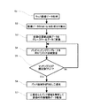
次に針跡の検査について説明する。以下の一連の動作は針跡検査用プログラム46に従って行われる。図4のフローチャートに示すようにまずプローブテスト後のウェハWを照明手段28で照明し、上カメラ72で撮像してウェハW上面の画像を、RGB成分を有するカラーの撮像データD1として取得し、RAM42に記憶する(ステップS1)。続いて図6(後述する図19参照)に示すように撮像データD1からR(Red)成分、G(Green)成分、B(Blue)成分の各成分を抽出して夫々のグレイデータである、R成分データD2、G成分データD3、B成分データD4を取得する(ステップS2)。
Next, needle mark inspection will be described. The following series of operations is performed according to the needle trace inspection program 46. As shown in the flowchart of FIG. 4, the wafer W after the probe test is first illuminated by the
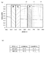
これ以降の動作を詳述する前に、その概要及び目的を簡単に述べて置く。図7(a)は、縦軸に相対反射率、横軸に光の波長をとり、銅、アルミニウム、シリコン夫々について両者の関係を示すグラフであり、破線L1は銅、実線L2はアルミニウム、一点鎖線L3は基台5のシリコンを示す。この図から分かるように銅は紫色の光(波長400nm)に対する相対反射率が47.5%と低く、波長が長くなるに従って相対反射率が高くなり赤色の光(波長700nm)に対する相対反射率が97.5%となる。これに対しアルミニウムの場合、紫色の光に対する相対反射率が94.8%、赤色の光で89.9%となり、光の波長の変化によって相対反射率はあまり変化せず高い値を示す。一方シリコンは、どのような光の波長に対しても相対反射率は50%以下となる。
Before describing the subsequent operations in detail, the outline and purpose will be briefly described. FIG. 7A is a graph showing the relative reflectance on the vertical axis and the wavelength of light on the horizontal axis, showing the relationship between copper, aluminum, and silicon. The broken line L1 is copper, the solid line L2 is aluminum, and one point. A chain line L3 indicates silicon of the
本発明は、このように各材質と光の波長によって相対反射率が異なる点に着目し、この特性を利用して下地層6の露出領域11(銅の露出領域)の検出を行っている。つまり本実施形態では、銅とアルミニウムの相対反射率の差が最も大きくなる紫色の光の波長に最も近いB成分データD4を用いることによって電極パッド2の材質であるアルミニウムと下地層6の露出領域11に現れる銅とを区別するようにしている。そしてB成分データD4に対してこのような区別を行うと基台5のシリコンの反射率が低いことから後のデータ処理がやり辛くなり、さらに基台5の影響を排除するために電極パッド2を切り出した場合でも、電極パッド2全体領域についてこのような区別を行うとデータ処理の負荷が大きくなるためB成分データD4の処理対象領域を針跡領域に絞るようにしている。
The present invention pays attention to the fact that the relative reflectance varies depending on the material and the wavelength of light as described above, and detects the exposed region 11 (copper exposed region) of the
このような観点に基づいて具体的には次のような処理が行われる(後述する図20参照)。即ちG成分データD3をグレースケール変換してGグレイデータD31を取得する(ステップS3)。G成分データD3では、アルミニウムの相対反射率が高く電極パッド2の部分が明るく写るため、GグレイデータD31に変換すると電極パッド2部分のグレイレベルが全体的に高くなる。そしてGグレイデータD31の全ての画素に対して、画面上をスキャンして画素の座標位置とそのグレイレベルを対応させたデータを取得してRAM42に記憶し、グレイレベルの高い連続した領域を検出すると共に領域の図示X軸方向及びY軸方向の端部の座標を検出してこれを繋ぐ矩形を検出する。
Specifically, the following processing is performed based on such a viewpoint (see FIG. 20 described later). That is, the G component data D3 is subjected to gray scale conversion to obtain G gray data D31 (step S3). In the G component data D3, since the relative reflectance of aluminum is high and the portion of the
矩形を検出したら、予め記憶されている電極パッド2のマッチングテンプレートを読み出してその矩形と比較する(ステップS4)。図8はこのような一連の処理のイメージを示している。D31はGグレイデータ、T1はマッチングテンプレートである。そしてマッチングテンプレートT1と検出した矩形の一致率が、規定値例えば90%以上になった場合には、検出した矩形が電極パッド2の領域であると判定し、逆にそれ以下の場合には検出をやり直す(ステップS5)。
When a rectangle is detected, a pre-stored matching template of the
ステップS4、S5を繰り返してGグレイデータD31の全領域で電極パッド2の検出が完了すると、検出した個々の電極パッド2の領域について針跡10の位置特定(抽出)を行う。まず図9に示すように切り出された電極パッド2の画像について、二値化する(ステップS6)。この領域では、上述したように電極パッド2の領域はグレイレベルが高くなるのに対し、針跡10では、その縁部の影や削り屑の影の位置、さらに針跡10に露出領域11が形成されていた場合には銅の相対反射率が電極パッド2より低いため露出領域11の位置で画素のグレイレベルが低くなる。そのため二値化を行うと、電極パッド2の領域のうち、縁部10aや削り屑の影12、露出領域11の部分の画素が0、その他の領域が1となったG二値化データD32が取得される。
When the detection of the
G二値化データD32を取得した後、G二値化データD32に対して、GグレイデータD31に対して行った画素の探索と同様の探索を行う。このとき例えばRAM42に最大X位置、最小X位置、最大Y位置、最小Y位置の各座標を記憶する領域を確保しておき、最初に値が0の画素が発見された場合、その画素の座標を上記記憶領域全てに記憶する。そして探索を続行し、次に値が0の画素が発見された場合、記憶されている各座標と夫々X、Y座標を比較して発見された座標の値がより最適な値である場合、例えばXの値が最大X位置の記憶領域に記憶されている値より大きい場合には、発見された座標を夫々の記憶領域に上書きする。
After obtaining the G binarized data D32, a search similar to the pixel search performed on the G gray data D31 is performed on the G binarized data D32. At this time, for example, an area for storing the coordinates of the maximum X position, the minimum X position, the maximum Y position, and the minimum Y position is secured in the
これにより針跡10のX−Y平面上の最も外側にある画素の位置が判り、この座標位置を基に針跡10と一致する、例えば針跡10の外周側に接する矩形状の針跡領域13と、その座標位置とを検出してそのデータをRAM42に記憶させる(ステップS7)。そしてステップS6、S7を繰り返して全ての電極パッド2ごとの針跡領域13及びその座標位置を検出してそのデータをRAM42に記憶させる。
As a result, the position of the pixel on the outermost side of the
尚本実施形態では電極パッド2の領域を二値化する際に使用するグレイレベルの閾値をRAM42に記憶しておき、その閾値を読み出しているが、本発明の実施の形態はこれに限らず、例えば電極パッド2の領域における画素のグレイレベルを調べ、グレイレベルを横軸、画素数を縦軸としたヒストグラムを生成し、このヒストグラムのピーク等の形状を基に閾値を決定してもよい。
In this embodiment, the gray level threshold value used when binarizing the region of the
全ての針跡領域13を検出した後、図5のフローチャートに示すように、まず図10(a)のようにB成分データD4をグレースケール変換してBグレイデータD41を取得する(ステップS21)。そしてBグレイデータD41から針跡領域13に対応する領域のデータを切り出して図10(b)に示すようにB針跡領域13bを取得し、B針跡領域13bから図11(a)に示すようなグレイレベルを横軸、画素数を縦軸としたヒストグラムを生成する(ステップS22)。
After all the
ヒストグラムを生成した後、図11(b)に示すように予め設定されているグレイレベルの範囲内のヒストグラムCを抽出する。このグレイレベルの範囲は、下地層6の銅と電極パッド2のアルミニウムとの反射率の差を基に、下地層6と電極パッド2との領域の切り分けができる範囲、つまり銅の検出範囲として設定されたグレイレベルの範囲であり、本実施形態では、グレイレベルの値が70から100までの間の範囲が、上記範囲として設定されている。そしてヒストグラムCから周知の方法により存在する全てのピークを検出する(ステップS23)。
After generating the histogram, as shown in FIG. 11B, a histogram C within a preset gray level range is extracted. This gray level range is a range in which the region between the
本実施形態では電極パッド2にアルミニウムを使用し下地層6に銅を使用しているため、B成分データD4では、下地層6が露出している露出領域11の相対反射率が電極パッド2の相対反射率に比べて低くなり、電極パッド2の領域に比べて露出領域11が暗く写る。そのためBグレイデータD41では露出領域11が形成された場合、露出領域11のグレイレベルが電極パッド2の領域の比べて低くなる。またBグレイデータD41では銅のグレイレベルが、上述した銅の検出範囲に対応するグレイレベルの範囲内の値になるため、露出領域11が形成された状態でヒストグラムを生成すると露出領域11に対応するグレイレベルの画素数が多くなり、ヒストグラムC内に特徴的、例えば他のピークに比べて明らかに大きいピークが形成される(ステップS24)。従ってこの特徴的なピークが検出された場合には露出領域11が形成されていることが判る。
In this embodiment, since aluminum is used for the
この特徴的なピークの検出は周知の方法(例えば、ローパスフィルタ処理等)により行われる。そして特徴的なピーク、例えば図11(b)に示すピークP1が検出できた場合には、ピークP1の始点P2と終点P3のグレイレベルの値をB針跡領域13bを二値化する際の閾値の上限及び下限として設定する(ステップS25)。尚露出領域11に対応するピークP1が発見できない場合、検出中のB針跡領域13bに対応する電極パッド2については、露出領域11がないと判断して検出を打ち切り、その情報をRAM42に記憶させる(ステップS30)。
This characteristic peak detection is performed by a known method (for example, a low-pass filter process). When a characteristic peak, for example, the peak P1 shown in FIG. 11B can be detected, the gray level values of the start point P2 and the end point P3 of the peak P1 are binarized in the B
閾値の範囲が設定されると、図10(c)に示すようにその閾値の範囲を基にB針跡領域13bを二値化してB針跡領域13bの画素のうち、閾値内のグレイレベルの画素を「0」とし、閾値から外れたグレイレベルの画素については「1」とする。そして銅の露出した露出領域11の画素及び閾値内の画素の領域が黒く、その他の領域が白いB二値化データD42が取得され、そのデータがRAM42に記憶される(ステップS26)。そして上述したステップS21〜S24を繰り返し、全ての電極パッド2についてピークP1の検出及び電極パッド2ごとのB二値化データD42を取得して、そのデータをRAM42に記憶させる。
When the threshold range is set, as shown in FIG. 10C, the B
こうして得られたB二値化データD42は、グレイレベルの閾値の範囲内に針跡10の縁部やアルミニウムの影に対応するグレイレベルが含まれてしまう場合があり、そうすると銅の露出領域11だけでなく、これらの影に対応する領域も「0」(黒画素)として表されてしまう。そこでこれら領域を切り分けるために、既に収録されてRAM42に記憶されているR成分データD2を用い、前記影に対してマスクをかけるマスク処理を行うようにしている。即ちまず図12(後述する図21参照)に示すようにR成分データD2を二値化し、マスクデータD21を取得する(ステップS27)。図12中、10aが縁部の影、12は削り滓の影である。R成分データD2では、電極パッド2のアルミニウムと下地層6の銅の相対反射率に差がないため、露出領域11が比較的明るく写り、縁部10aの影や削り屑の影12の領域のみが暗く写る。そのためマスクデータD21を取得すると図12に示すように影の部分に対応する画素のみが0となり、その他の部分の画素は1となる。
The B binarization data D42 obtained in this way may include a gray level corresponding to the edge of the
このマスクデータD21に対して既述のようにして針跡領域13を切り出し、切り出されたマスクデータD21を用いてB二値化データD42に対するマスク処理を行う。即ちマスクデータD21の「0」の画素と重なるB二値化データD42の「0」の画素を「1」に置き換える(ステップS28)。この処理によれば図13に示すB二値化データD42における黒領域から縁部の影10aや削り屑の影12に対応する黒領域を除去する処理に相当し、結果として銅の露出領域11を黒領域とする針跡領域13の画像が得られることになる。この画像データを露出位置特定データ15と呼ぶことにする。そしてこの露出位置特定データ15は、RAM42に記憶される(ステップ29)。そしてステップS25〜S27を繰り返して、全てのB二値化データD42に対してマスク処理を行い、マスク処理後の露出位置特定データ15を取得して、そのデータをRAM42に記憶させる。
As described above, the
その後RAM42から各電極パッド2に対応する針跡10に関する情報を読み出し、例えば針跡10のない電極パッド2を含むICチップについては再検査の表示を付し、露出位置特定データ15において銅の露出領域として取り扱っている「0」の画素の数が予め設定した画素数を超えている電極パッド2を含むチップ1、例えば「0」の画素が1個でも存在したチップ1については針跡10が深堀りである等の情報をそのチップ1に付しRAM42に記憶する。このような情報が取得された後の処理についての一例を述べると、深堀りと判断された電極パッド2について、その電極パッド2の例えばRGB成分が混在する大元の画像をオペレータが表示部に表示させ、オペレータにより深堀りの判断が適切か否かを確認するようにしてもよく、最終的に深堀りと判断されればその電極パッド2を含むチップ1を不良品として取り扱う。またこうしたオペレータの確認を行なわなくてもよいことは勿論である。針跡検査の結果を例えばウェハW上のチップ1の位置に対応付けて表示部に表示させ、例えば各チップ1にその結果に対応した色分け等を行うようにしてもよい。
Thereafter, information on the needle traces 10 corresponding to the
尚本実施形態では、ステップS1、ステップS2に対応する工程をRGB成分取得部50が、ステップS3からステップS7に対応する工程を針跡領域抽出部51が、ステップS21からステップS25、及びステップS30に対応する工程をB成分ヒストグラム取得部52が、ステップS26に対応する工程をB成分二値化部53が、ステップS27からステップS29に対応する工程をマスク処理部54が、夫々行っている。
In the present embodiment, the RGB
以上上述した本実施形態のプローブ装置は、針跡10の検査を行う際にカラーデータである撮像データD1を取得し、撮像データD1から抽出されるR成分データD2、G成分データD3、B成分データD4のうち、電極パッド2の材質であるアルミニウムにおける光の相対反射率と下地層6の材質である銅の光の相対反射率との差が最も大きくなるB成分データD4を下地層の露出判定用データとして選択している。そしてB成分データD4から針跡領域13を切り出してグレイレベルと画素数とのヒストグラムを生成し、そのヒストグラムから下地層6の銅に対応するグレイレベルの範囲内におけるピークP1を検出してこのピークP1に対応するグレイレベルを閾値の範囲としてB二値化データD42を取得している。更にR成分データD2を用いたマスク処理を行うことによって削り滓の影12等に対応する領域を除去するようにしている。従ってプローブ針33によるパッド2の深堀り(下地層6まで掘ってしまう状態)を自動で速やかに精度良く確実に検出することができ、オペレータの負担も大幅に軽減できる。またプローブ装置内にて針跡10の検査を行うことができるので従来のようにオペレータによる金属顕微鏡の作業領域にウェハWを搬送しなくても済み、更にプローブ針の異常やオーバドライブの異常などを速やかに把握することができる。
The probe device of the present embodiment described above acquires the imaging data D1 that is color data when the
また本実施形態では、撮像データD1からR成分データD2、G成分データD3、B成分データD4を抽出し、R成分データD2をマスク処理に、G成分データD3を針跡位置検出処理に、B成分データD4を下地層露出判定処理に使用している。そのため実際の処理を行うデータは、撮像データD1に比べてデータ量が少なくなるので、各処理の効率化が図れる。 In this embodiment, R component data D2, G component data D3, and B component data D4 are extracted from the imaging data D1, R component data D2 is used for mask processing, G component data D3 is used for needle trace position detection processing, B The component data D4 is used for the underlayer exposure determination process. For this reason, the amount of data to be actually processed is smaller than that of the imaging data D1, so that the efficiency of each process can be improved.
上述の実施形態では、B二値化データD42に対してR成分データD2を利用してマスク処理をかけており、このため針跡10の縁やアルミニウムの削り滓の影と銅の露出領域とを分離できる利点があるが、本発明の実施形態としてはマスク処理を行わなくてもよい。この場合は、例えばアルミニウムの削り滓等の陰の領域の面積(画素数)を実験データに基づいて決めておき、B二値化データD42における黒領域の画素数から影の領域の画素数を差し引いたデータを用いて銅の露出領域の有無を判定することができる。また上述の実施形態では電極パッド2を撮像するたびに(毎回)、B成分データD4に対して図7に示すヒストグラムを求めてグレイレベルの閾値を求めているが、例えばウェハWの種別毎に予め前記閾値を求めてRAM42に格納しておき、針跡検査の対象となるウェハWの種別に応じて閾値を読み出してその閾値を用いてB成分の二値化データを作成するようにしてもよい。そしてこのB成分の二値化データから、電極パッドの削り滓の影等の画素を除去してそのB成分の二値化データを探索し、「0」の画素を発見することで露出領域の有無を判定するようにしてもよい。
In the above-described embodiment, the B binarization data D42 is masked using the R component data D2, and for this reason, the edge of the
ところで図7に示すヒストグラムに基づいて求めた閾値は、その閾値よりもグレイレベルが高い画素、つまり銅の露出領域に対応する画素を抽出するためのものであるから、例えばこの閾値に基づいて二値化データを作成せずに当該閾値よりもグレイレベルが高い画素の数をカウントし、そのカウント値から針跡10の縁やアルミニウムの影に相当する領域について、予め設定した画素数を差し引き、得られた画素数に基づいて銅の露出領域の有無を判定するようにしてもよい。また画素数ではなく、グレイレベルが高い画素の領域の面積を位置座標から求め、その領域の面積に応じて銅の露出領域の有無を判定するようにしてもよい。
By the way, the threshold value obtained based on the histogram shown in FIG. 7 is for extracting a pixel having a gray level higher than the threshold value, that is, a pixel corresponding to the exposed region of copper. The number of pixels having a gray level higher than the threshold value is counted without creating the digitized data, and the preset number of pixels is subtracted from the count value for the area corresponding to the edge of the
そしてまた本発明は、R、G、Bの各成分の中から電極パッドの材質と下地層の材質との反射率の差に応じて適切な成分、即ち一方の材質を特定するグレイレベルの範囲内に他方の材質を特定するグレイレベルが重ならずに有効に両者を切り分けることができる程度の反射率の差がある波長成分を選択して、既述のようにして下地層の露出領域を検出するものであることから、電極パッドの材質や下地層の材質は夫々、銅、アルミニウムに限られるものではなく、使用する各材質に応じてR、G、Bのいずれかの成分の画像を利用すればよい。ここで本発明の針跡検出装置は、プローブ装置に組み合わせて設けることに限らず、スタンドアローンとして構成してもよい。また本実施形態では、針跡領域の検出にG成分のデータを使用していたが、本発明の実施の形態としては、パッド領域の特定、針跡領域の検出、及び下地層の露出判定が可能であれば、単一のカラー成分のデータ、例えばB成分のデータのみを用いてパッド領域の特定及び針跡領域の検出と、針跡領域のヒストグラムの取得を行い、露出の有無を判定するように構成することも可能である。 The present invention also provides an appropriate component, that is, a gray level range for specifying one of the R, G, and B components according to the difference in reflectance between the electrode pad material and the underlayer material. Select the wavelength component that has a difference in reflectivity so that the gray level that identifies the other material can be effectively separated without overlapping, and the exposed area of the underlayer is set as described above. Since it is to be detected, the material of the electrode pad and the material of the base layer are not limited to copper and aluminum, respectively, and an image of any component of R, G, or B can be obtained depending on each material used. Use it. Here, the needle mark detection device of the present invention is not limited to being provided in combination with the probe device, but may be configured as a stand-alone device. In this embodiment, the G component data is used for detection of the needle trace area. However, in the embodiment of the present invention, the specification of the pad area, the detection of the needle trace area, and the exposure determination of the underlayer are performed. If possible, use only a single color component data, for example, B component data, to identify the pad area, detect the needle trace area, and acquire a histogram of the needle trace area to determine the presence or absence of exposure. It is also possible to configure as described above.
[第2の実施形態]
本発明は、電極パッドのカラー画像を取得してその画像のR、G、B成分に対応する画像を取得し、その各成分データのうち、電極パッドの反射率と下地層の反射率の差がそれらの成分の中で最も大きくなる成分データを利用して露出領域を検出する針跡検査装置である。従ってウェハWの撮像する手段は、第1の実施形態の上カメラ72に限らず、例えば別途専用のカメラを上カメラ72とは異なる場所、例えばヘッドプレート等に設けても良い。また撮像手段としても、上カメラ72のようなR、G、B成分を含むカラー画像が取得可能なカラーカメラに限らず、例えば、R、G、B、夫々の成分を専用に取得する3台のカメラを組み合わせて撮像手段を構成してもよい。
[Second Embodiment]
The present invention acquires a color image of an electrode pad and acquires an image corresponding to the R, G, and B components of the image, and the difference between the reflectance of the electrode pad and the reflectance of the underlying layer in each component data. Is a needle trace inspection device that detects an exposure region using component data that is the largest of these components. Therefore, the means for imaging the wafer W is not limited to the
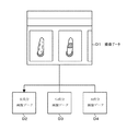
以上の事から本発明の実施の形態としては、次の第2の実施形態に示す形態であってもよい。この第2の実施形態のプローブ装置では、図14に示すように上述したR成分の撮像データのみを取得するRカメラ73a、G成分の撮像データのみ取得するGカメラ73b、B成分の撮像データのみ取得するBカメラ73cを組み合わせたカメラユニット73をヘッドプレート30に設けており、このカメラユニット73によって、プローブカード32の側方からプローブ針33と電極パッド2が接触した直後の画像を撮像する。またカメラユニット73は照明手段28aを備えている。そしてカメラユニット73は、ウェハWを撮像する際に撮像データD1を入手するのではなく、R成分データD2、G成分データD3、B成分データD4を各カメラ73a〜73cで取得する。このような実施の形態においても、B成分データD4を下地層の露出判定用データとして選択して、例えば第1の実施形態と同様の処理を行うことができる。
From the above, the embodiment of the present invention may be the embodiment shown in the following second embodiment. In the probe apparatus of the second embodiment, as shown in FIG. 14, the
また本実施形態においては、ウェハWを撮像する際に上カメラ72が移動させるためにヘッドプレート30を退避させる必要がなく、プローブテスト直後にカメラユニット73にて各成分データD2〜D4を取得し、露出領域11とその位置の検出を行うことが可能となるので検査効率を向上させることができる。尚本実施形態においては、カメラユニット73の各カメラ73a〜73cにフィルタユニットを設けて、下地層6の材質におけるR成分、G成分、B成分の光の反射率から設定された抽出用閾値を基にフィルタリングを行い、下地層6の材質と対応する各成分グレイレベルの範囲内の画素のみを抽出してデータD2〜D4を取得するようにしてもよい。またカメラユニット73は、RGB各成分のデータD2〜D4を夫々別々のカメラ73a〜73cで撮像する構成になっていることから、各カメラ73a〜73cでRGB各成分データD2〜D4が鮮明に撮像可能となるように、照明手段28の光の各成分における光度を調整して各カメラ73a〜73cの撮像タイミングをずらすようにしてもよい。
Further, in this embodiment, it is not necessary to retract the
[第3の実施形態]
また本発明の実施の形態としては、次の第3の実施形態に示す形態であってもよい。この第3の実施形態のプローブ装置では、第1の実施形態で備えられていた上カメラ72と照明手段28の代わりに、図15に示すような撮像データD1をモノクロ画像として取得可能な上カメラ72mが備えられ、さらにウェハWを照明するための例えば発光ダイオードからなる、R照明手段28r、G照明手段28g、B照明手段28bが備えられている。R照明手段28rは赤色の光で、G照明手段28gは緑色の光で、B照明手段28bは青色の光でウェハWを照明する。これにより上カメラ72mでは、各照明手段28r、28g、28bから順番に照明された光に対応する成分の画像データのみ取得することが可能となるので、第2の実施形態と同様にR成分データD2、G成分データD3、B成分データD4を個々に取得することになる。このような実施の形態においても、B成分データD4を下地層の露出判定用データとして選択して、例えば第1の実施形態と同様の処理を行うことができる。また本実施形態においては、R照明手段28r、G照明手段28g、B照明手段28bの光の強さを調整するだけで、RGB各成分データD2〜D4が鮮明に撮像可能となる。
[Third Embodiment]
Further, the embodiment of the present invention may be the embodiment shown in the following third embodiment. In the probe device of the third embodiment, instead of the
以上本発明の各実施形態について説明したが、本発明は上述の実施の形態に限定されるものではない。例えば図16に示すように、露出位置特定部52は、ヒストグラムを生成した際に予め定められたBグレイデータD41における下地層6に対応するグレイレベルの標準サンプルh1を基に、従来知られている最大誘導法等を用いてヒストグラムをスムージングしてグレイレベルのばらつきを吸収するようにしてもよい。これにより下地層6の銅の酸化や、針跡10の形状の差異、上カメラ72と照明手段28の角度や光度等によって生じるグレイレベルのばらつきを吸収することが可能となる。そのためカラーデータを取得可能な撮像手段を使用した場合に発生する、例えば下地の銅が酸化によって変色したり、撮像データが光源に依存して撮像データそのものが変化して、その結果色の見え方が変化してデータに幅が生じるという問題に対して対処可能となる。そして本実施形態の制御部4による、露出領域11とその位置検出の精度をより一層向上させることが可能となる。
Although each embodiment of the present invention has been described above, the present invention is not limited to the above-described embodiment. For example, as shown in FIG. 16, the exposure
次に本発明の針跡検査装置を備えたプローブ装置の具体的な運用方法について、図17、18を参照して説明する。まず第1の運用方法として、図17のフローに示すように、プローブ針33と電極パッド2とを接触させて最初のプローブテストを行い(ステップS31)、プローブテスト終了後に撮像手段である上カメラ72、若しくはカメラユニット73(以下、単に撮像手段とする)にてウェハWの検査領域全体を撮像して撮像データD1を取得する(ステップS32)。次に撮像データD1から画像抽出部50にてG成分データD3を抽出し、G成分データD3より針跡10を検出する(ステップS33)。針跡検査後、例えば針跡10における1の画素の許容数を決めておき、その許容数を上回る1の画素を有する針跡10が形成された電極パッド2、つまり露出領域11が形成された可能性のある電極パッド2を抽出する。(ステップS34)。
Next, a specific operation method of the probe apparatus provided with the needle trace inspection apparatus of the present invention will be described with reference to FIGS. First, as a first operation method, as shown in the flow of FIG. 17, the
そして抽出された電極パッド2のみを撮像手段にて撮像し(ステップS35)、B成分データD4、R成分データD2を新規で取得して露出位置特定部52、マスク処理部53で処理を行い、電極パッド2に露出領域11が形成されているかどうかを判定する(ステップS36)。この運用方法によれば、最初にプローブ針33が電極パッド2に対して露出領域11が形成される程強く接触したことが判るので、その後の試験で電極パッド2に下地層6の銅が付着することを防止でき、またプローブ針33と電極パッド2とのコンタクト位置の微調整を行うことも可能となる。
Then, only the extracted
次に第2の運用方法として、図18のフローに示すように、プローブテスト終了後に全てのチップ1についてのプローブテストの結果を調べる。プローブテスト時にプローブ針33の先端が下地層6に到達した場合、プローブテストの結果が予め定めた特定BINの範囲に入るため、そのチップ1の位置を検出する(ステップS41)。そしてそのチップ1の電極パッド2を撮像手段により撮像し(ステップS42)、針跡位置特定部50にてG成分データD3から針跡位置を特定する。(ステップS43)。次にステップS34と同様の方法により露出領域11が形成されている可能性のある電極パッド2を抽出し(ステップS44)、B成分データD4、R成分データD2から、露出位置特定部52、マスク処理部53で処理を行い、電極パッド2に露出領域11が形成されているかどうかを判定する(ステップS45)。この運用方法によれば、プローブテスト後の結果から電極パッド2に露出領域11が形成された可能性のあるチップ1のみを検査することができるので検査効率を向上させることができる。
Next, as a second operation method, as shown in the flow of FIG. 18, the probe test results for all the
次に本発明の効果を確認するために行った実験について説明する。まず第1の実験として第1の実施形態に係るプローブ装置を用い、上カメラ72にてウェハWを撮像して、ウェハWの全面に対応する、例えば39分割された撮像データD1を取得する。次にウェハWを金属顕微鏡で目視して、露出領域11の画素を0、それ以外の画素を1と置き換えて二値化した画像、つまり人間が目で見て作成した所謂Ground Truth画像(以下、単にGT画像)を取得し、その中から例えば75個の電極パッド2をサンプルとして選択する。そしてGT画像から検出した露出領域11が形成された電極パッド2の数と、撮像データD1を制御部4にて検出した結果とを比較して露出領域11の検出精度を調べた。尚実験では、サンプルとして使用した75個の電極パッド2のうち53個の電極パッド2に露出領域11が形成されている。この第1の実験の結果を表1に示す。
Next, experiments conducted for confirming the effects of the present invention will be described. First, as a first experiment, using the probe apparatus according to the first embodiment, the
第1の実験では、以下の表1に示すように露出領域11が形成されている電極パッド2については全て露出領域11が形成されていることを検出した。一方露出領域11が検出されていない22個の電極パッド2については、22個中4個の電極パッド2について、露出領域11が形成されていると誤検出している。この誤検出した電極パッド2について実物を調べた所、電極パッド2に画素単位の非常に小さな下地層6の銅が付着している部分があり、この部分を露出領域11と誤認識したことが原因であった。言い換えれば制御部4では、金属顕微鏡にて検出できない微細な銅が付着した電極パッド2についても露出領域11有りとして検出できることになる。電極パッド2に銅が付着した場合、チップ1の電気的特性に悪影響を及ぼす虞があるため、そのようなチップ1については不良品となっており、このことから本実施形態の針跡検査装置では、露出領域11の検出精度が非常に高く、更に金属顕微鏡等による目視では検出不可能な不良品となるチップ1についても不良品と判定することができる。また微細な銅の検出ができるため、プローブ針33の汚染チェックを行うことも可能となる。また、この誤認識を抑制し露出面のみを検出する方法としては、二値化画像による露出位置検出時に、一定の面積以下の部分を排除する閾値を設けることで100%の正答を得ることが可能となる。
In the first experiment, as shown in Table 1 below, it was detected that the exposed

次に第2の実験として、第1の実施形態のプローブ装置を用い、ウェハW上の電極パッド2について露出領域11の検出を1分間行い、何枚の電極パッド2について検査を行えたのかを調べた。また比較対象として従来と同様に金属顕微鏡等を使用して同じウェハWについて検査を行い、何枚の電極パッド2について検査を行えたのか調べた。プローブ装置の制御部4では、撮像データD1を取得してから1個の電極パッド2について露出領域11が形成されているか検出して判定するのに平均して約45mSecを要す。そして本実施形態の制御部4では、撮像データD1の取得等に15秒必要となるので、1分間で約1000枚の電極パッド2について露出領域11の検出を行うことができた。
Next, as a second experiment, using the probe apparatus of the first embodiment, the
一方従来の金属顕微鏡による検出では、1個の電極パッド2について露出領域11が形成されているか検出して判定するのに平均して約200〜500mSecを要し、ウェハWの位置決め等に掛かる時間も必要となることから、1分間で約20枚の電極パッド2について検出を行うことができるのみであった。更にこの検出方法では、作業従事者の疲労や集中力低下、検査従事者の個人的力量の差によって検査時間が変化することから、常に一定のペースで長時間連続的に検出を行うことは不可能である。これに対し、本実施形態のプローブ装置では、制御部4によって検出を行うことから長時間連続的に検出を行うことが可能となり、また検出速度も金属顕微鏡による検査に対して約500倍の速さで行うことが可能となるため、検査効率を大幅に向上させることができる。上記二つの実験結果から、本実施形態の針跡検査装置では、従来の金属顕微鏡等を用いて行う検査と比較して、精度、検査速度、共に優れていることが判る。
On the other hand, in the detection by the conventional metallurgical microscope, it takes about 200 to 500 mSec on average to detect and determine whether or not the exposed
次に第1の実施形態の針跡検査装置で行った針跡10の検出について、実際のウェハWの撮像データを参照しながら説明する。まず図19に示すように、ステップS1、ステップS2に対応する工程を行い、撮像データD1を取得して撮像データD1からR成分データD2、G成分データD3、B成分データD4を取得している。次に図20に示すように、ステップS3、ステップS4、ステップS5、ステップ6、ステップ7に対応する工程を行い、図20(a)に示すG成分データD3からGグレイデータD31を取得して画素の探索を行い、図20(b)に示すマッチングテンプレートT1を用いて電極パッド2の領域を検出する。そして図20(c)に示すように全ての電極パッド2の領域を検出したら、図20(d)に示す電極パッド2の領域を二値化して針跡領域13を検出する工程を行う。
Next, detection of the
そして、上述したステップS21からステップS26までの工程を行い、B二値化データD42を取得したら、図21に示すようにステップS27の工程を行い、R成分データD2を二値化してマスクデータD21を取得し、このマスクデータD21を基に上述したマスク処理を行って露出領域11の有無及び位置を特性する。以上の工程を行うことによって本実施形態の針跡検査装置では、針跡10に対応する針跡領域13の検出、露出領域11の有無の検出、露出領域11の位置特定を行う。
Then, when the processes from step S21 to step S26 described above are performed and the B binarized data D42 is acquired, the process of step S27 is performed as shown in FIG. 21 to binarize the R component data D2 and mask data D21. And the above-described mask processing is performed based on the mask data D21 to characterize the presence and position of the exposed
1 チップ
2 電極パッド
4 制御部
6 下地層
10 針跡
10a 縁部の影
11 露出領域
12 削り屑の影
13 針跡領域
13b B針跡領域
15 露出位置特定データ
21 第1ステージ
22 第2ステージ
23 第3ステージ
24 チャックトップ
28、28a 照明手段
28b B照明手段
28g G照明手段
28r R照明手段
30 ヘッドプレート
33 プローブ針
34 カメラ搬送部
41 RAM
45 プロービング用プログラム
46 針跡検査用プログラム
50 RGB成分取得部
51 針跡領域抽出部
52 B成分ヒストグラム取得部
53 B成分二値化部
54 マスク処理部
72、72m 上カメラ(撮像手段)
73 カメラユニット(撮像手段群)
73a Rカメラ(R成分撮像手段)
73b Gカメラ(G成分撮像手段)
73c Bカメラ(B成分撮像手段)
D1 撮像データ
D2 R成分データ
D3 G成分データ
D4 B成分データ
D21 マスクデータ
D31 Gグレイデータ
D32 G二値化データ
D41 Bグレイデータ
D42 B二値化データ
P1 ピーク
W ウェハ
DESCRIPTION OF
45 Probing program 46 Needle
73 Camera unit (imaging means group)
73a R camera (R component imaging means)
73b G camera (G component imaging means)
73c B camera (B component imaging means)
D1 Imaging data D2 R component data D3 G component data D4 B component data D21 Mask data D31 G gray data D32 G binarization data D41 B gray data D42 B binarization data P1 Peak W Wafer
Claims (21)
カラー成分であるR成分、G成分及びB成分の中から、電極パッドの材質と下地層の材質との反射率の差に応じて選択されたカラー成分の画像データである、画素の座標位置とグレイレベルとを対応付けたグレイデータを取得する手段と、
この手段で取得された前記グレイデータと、前記電極パッドの材質と下地層の材質とを区別するための前記選択されたカラー成分のグレイレベルのしきい値と、に基づいて、針跡における下地層の露出の有無を判定する手段と、を備えたことを特徴とする針跡検査装置。 After performing electrical measurement by bringing the probe needle into contact with the electrode pad on the substrate to be inspected, the needle trace formed on the electrode pad is imaged, and the presence or absence of exposure of the underlying layer of the electrode pad is inspected. A device,
The pixel coordinate position, which is image data of a color component selected according to the difference in reflectance between the material of the electrode pad and the material of the underlayer from among the R component, G component, and B component that are color components Means for acquiring gray data in association with gray levels ;
Based on the gray data obtained by this means and the gray level threshold value of the selected color component for distinguishing between the material of the electrode pad and the material of the underlayer , And a means for determining the presence or absence of exposure of the formation.
請求項1ないし10の何れか一項に記載の針跡検査装置を備えたことを特徴とするプローブ装置。 The probe apparatus which mounts a board | substrate on a probe card and a mounting base, and makes the probe needle of a probe card contact the electrode pad of the chip | tip on a board | substrate, and performs the electrical measurement of a chip | tip. A probe device comprising the needle trace inspection device according to 1.
カラー成分であるR成分、G成分及びB成分の中から、電極パッドの材質と下地層の材質との反射率の差に応じて選択されたカラー成分の画像データである、画素の座標位置とグレイレベルとを対応付けたグレイデータを取得する工程と、
この工程で取得された前記グレイデータと、前記電極パッドの材質と下地層の材質とを区別するための前記選択されたカラー成分のグレイレベルのしきい値と、に基づいて、針跡における下地層の露出の有無を判定する工程と、を備えたことを特徴とする針跡検査方法。 After performing electrical measurement by bringing the probe needle into contact with the electrode pad on the substrate to be inspected, the needle trace formed on the electrode pad is imaged, and the presence or absence of exposure of the underlying layer of the electrode pad is inspected. A method,
The pixel coordinate position, which is image data of a color component selected according to the difference in reflectance between the material of the electrode pad and the material of the underlayer from among the R component, G component, and B component that are color components Obtaining gray data in association with gray levels ;
Based on the gray data acquired in this step and the gray level threshold value of the selected color component for distinguishing between the electrode pad material and the underlayer material, And a step of determining whether the formation is exposed or not.
前記針跡における下地層の露出の有無を判定する工程は、前記二値化画像データに基づいて行われることを特徴とする請求項12に記載の針跡検査方法。 Performing binarization processing on the gray data based on the gray level threshold value to obtain binarized image data ;
The needle trace inspection method according to claim 12 , wherein the step of determining whether or not the underlying layer is exposed in the needle trace is performed based on the binarized image data .
前記コンピュータプログラムは、請求項12ないし20のいずれか一つに記載の針跡検査方法を実行するようにステップ群が構成されていることを特徴とする記憶媒体。 After performing electrical measurement by bringing the probe needle into contact with the electrode pad on the substrate to be inspected, the needle trace formed on the electrode pad is imaged, and the presence or absence of exposure of the underlying layer of the electrode pad is inspected. A storage medium storing a computer program used in the apparatus,
A storage medium characterized in that the computer program includes a group of steps so as to execute the needle trace inspection method according to any one of claims 12 to 20.
Priority Applications (4)
| Application Number | Priority Date | Filing Date | Title |
|---|---|---|---|
| JP2008138353A JP5286938B2 (en) | 2008-05-27 | 2008-05-27 | Needle mark inspection device, probe device, needle mark inspection method, and storage medium |
| KR1020090041424A KR101230673B1 (en) | 2008-05-27 | 2009-05-12 | Probe mark inspection apparatus, probe apparatus, probe mark inspection method and storage medium |
| TW098117478A TWI505384B (en) | 2008-05-27 | 2009-05-26 | A stitch check device, a probe device and a stitch check method, and a memory medium |
| CN2009101452289A CN101593714B (en) | 2008-05-27 | 2009-05-27 | A needle tracking inspection device, a detecting device and a needle tracking inspection method |
Applications Claiming Priority (1)
| Application Number | Priority Date | Filing Date | Title |
|---|---|---|---|
| JP2008138353A JP5286938B2 (en) | 2008-05-27 | 2008-05-27 | Needle mark inspection device, probe device, needle mark inspection method, and storage medium |
Publications (3)
| Publication Number | Publication Date |
|---|---|
| JP2009289818A JP2009289818A (en) | 2009-12-10 |
| JP2009289818A5 JP2009289818A5 (en) | 2011-06-30 |
| JP5286938B2 true JP5286938B2 (en) | 2013-09-11 |
Family
ID=41408296
Family Applications (1)
| Application Number | Title | Priority Date | Filing Date |
|---|---|---|---|
| JP2008138353A Active JP5286938B2 (en) | 2008-05-27 | 2008-05-27 | Needle mark inspection device, probe device, needle mark inspection method, and storage medium |
Country Status (4)
| Country | Link |
|---|---|
| JP (1) | JP5286938B2 (en) |
| KR (1) | KR101230673B1 (en) |
| CN (1) | CN101593714B (en) |
| TW (1) | TWI505384B (en) |
Families Citing this family (6)
| Publication number | Priority date | Publication date | Assignee | Title |
|---|---|---|---|---|
| WO2011118596A1 (en) * | 2010-03-25 | 2011-09-29 | 三菱レイヨン株式会社 | Method for fabricating anodized alumina, inspection device, and inspection method |
| KR102317023B1 (en) * | 2014-08-14 | 2021-10-26 | 삼성전자주식회사 | semiconductor device, method and apparatus for manufacturing the same |
| US9747520B2 (en) * | 2015-03-16 | 2017-08-29 | Kla-Tencor Corporation | Systems and methods for enhancing inspection sensitivity of an inspection tool |
| JP6406221B2 (en) | 2015-11-17 | 2018-10-17 | 三菱電機株式会社 | Semiconductor device evaluation apparatus and evaluation method |
| JP2022133631A (en) | 2021-03-02 | 2022-09-14 | 株式会社東京精密 | Particle measurement device, three-dimensional shape measurement device, prober device, particle measurement system, and particle measurement method |
| TWI803353B (en) * | 2022-04-19 | 2023-05-21 | 南亞科技股份有限公司 | Wafer inspection method |
Family Cites Families (9)
| Publication number | Priority date | Publication date | Assignee | Title |
|---|---|---|---|---|
| JP2002252262A (en) * | 2001-02-23 | 2002-09-06 | Dainippon Screen Mfg Co Ltd | Method for detecting copper deposited substrate and substrate processing apparatus using the same |
| JP4828741B2 (en) * | 2001-08-23 | 2011-11-30 | 大日本スクリーン製造株式会社 | Probe mark measuring method and probe mark measuring apparatus |
| JP4357813B2 (en) * | 2002-08-23 | 2009-11-04 | 東京エレクトロン株式会社 | Probe apparatus and probe method |
| US7308157B2 (en) * | 2003-02-03 | 2007-12-11 | Photon Dynamics, Inc. | Method and apparatus for optical inspection of a display |
| JP4730895B2 (en) * | 2004-12-10 | 2011-07-20 | 大日本スクリーン製造株式会社 | Needle mark detection device and needle mark detection method |
| KR101047795B1 (en) * | 2005-01-05 | 2011-07-07 | 엘지이노텍 주식회사 | Semiconductor light emitting device |
| KR101170587B1 (en) * | 2005-01-05 | 2012-08-01 | 티에이치케이 인텍스 가부시키가이샤 | Method and device for breaking work, method for scribing and breaking work, and scribing device with breaking function |
| CN100541879C (en) * | 2005-05-17 | 2009-09-16 | Agc清美化学股份有限公司 | The manufacture method of the lithium-contained composite oxide that cathode plate for lithium secondary battery is used |
| JP4334527B2 (en) * | 2005-10-21 | 2009-09-30 | 大日本スクリーン製造株式会社 | Needle mark detection device and needle mark detection method |
-
2008
- 2008-05-27 JP JP2008138353A patent/JP5286938B2/en active Active
-
2009
- 2009-05-12 KR KR1020090041424A patent/KR101230673B1/en active IP Right Grant
- 2009-05-26 TW TW098117478A patent/TWI505384B/en active
- 2009-05-27 CN CN2009101452289A patent/CN101593714B/en active Active
Also Published As
| Publication number | Publication date |
|---|---|
| TW201009973A (en) | 2010-03-01 |
| TWI505384B (en) | 2015-10-21 |
| CN101593714B (en) | 2011-07-06 |
| JP2009289818A (en) | 2009-12-10 |
| KR20090123785A (en) | 2009-12-02 |
| CN101593714A (en) | 2009-12-02 |
| KR101230673B1 (en) | 2013-02-07 |
Similar Documents
| Publication | Publication Date | Title |
|---|---|---|
| TWI483325B (en) | A stitch check device, a probe device and a stitch check method, and a memory medium | |
| JP3051279B2 (en) | Bump appearance inspection method and bump appearance inspection device | |
| US6779159B2 (en) | Defect inspection method and defect inspection apparatus | |
| JP4595705B2 (en) | Substrate inspection device, parameter setting method and parameter setting device | |
| JP5286938B2 (en) | Needle mark inspection device, probe device, needle mark inspection method, and storage medium | |
| KR100786463B1 (en) | Method for aligning two objects, method for detecting superimposing state of two objects, and apparatus for aligning two objects | |
| JP5421763B2 (en) | Inspection apparatus and inspection method | |
| JP2011158363A (en) | Soldering inspection device for pga mounting substrate | |
| JP2009128303A (en) | Visual examination device for substrate | |
| JP5417197B2 (en) | Inspection apparatus and inspection method | |
| JP4506395B2 (en) | Substrate inspection device, parameter setting method and parameter setting device | |
| WO2003065018A2 (en) | System and method for inspection using dark and bright field illumination | |
| JP2009042093A (en) | Electronic component inspection device and electronic component inspection method | |
| JP4523310B2 (en) | Foreign matter identification method and foreign matter identification device | |
| JP4453503B2 (en) | Substrate inspection device, substrate inspection method, inspection logic generation device and inspection logic generation method for substrate inspection device | |
| JP2010266366A (en) | Characteristic extraction method of image, tool defect inspection method, and tool defect inspection device | |
| JP2002250700A (en) | Method and device for inspecting pattern | |
| JP2010139434A (en) | Test apparatus and test method for discriminating between foreign substance and scar | |
| JP3722052B2 (en) | Method and apparatus for evaluating pad portion for mounting semiconductor chip | |
| JP5096940B2 (en) | Inspection method and apparatus for printed wiring board | |
| JP2003270304A (en) | Probe device and method for recognizing probe tip | |
| KR100313092B1 (en) | Method for testing ball shape of wire bonding device | |
| JPH11285910A (en) | Inspection device for edge shape of drill | |
| JP2000146536A (en) | Method for measuring elongation of tension test | |
| JP2020046393A (en) | Device for inspecting chip body |
Legal Events
| Date | Code | Title | Description |
|---|---|---|---|
| A621 | Written request for application examination |
Free format text: JAPANESE INTERMEDIATE CODE: A621 Effective date: 20110329 |
|
| A521 | Request for written amendment filed |
Free format text: JAPANESE INTERMEDIATE CODE: A523 Effective date: 20110512 |
|
| A131 | Notification of reasons for refusal |
Free format text: JAPANESE INTERMEDIATE CODE: A131 Effective date: 20130205 |
|
| A977 | Report on retrieval |
Free format text: JAPANESE INTERMEDIATE CODE: A971007 Effective date: 20130207 |
|
| A521 | Request for written amendment filed |
Free format text: JAPANESE INTERMEDIATE CODE: A523 Effective date: 20130408 |
|
| TRDD | Decision of grant or rejection written | ||
| A01 | Written decision to grant a patent or to grant a registration (utility model) |
Free format text: JAPANESE INTERMEDIATE CODE: A01 Effective date: 20130507 |
|
| A61 | First payment of annual fees (during grant procedure) |
Free format text: JAPANESE INTERMEDIATE CODE: A61 Effective date: 20130520 |
|
| R150 | Certificate of patent or registration of utility model |
Ref document number: 5286938 Country of ref document: JP Free format text: JAPANESE INTERMEDIATE CODE: R150 |
|
| R250 | Receipt of annual fees |
Free format text: JAPANESE INTERMEDIATE CODE: R250 |
|
| R250 | Receipt of annual fees |
Free format text: JAPANESE INTERMEDIATE CODE: R250 |
|
| R250 | Receipt of annual fees |
Free format text: JAPANESE INTERMEDIATE CODE: R250 |
|
| R250 | Receipt of annual fees |
Free format text: JAPANESE INTERMEDIATE CODE: R250 |
|
| R250 | Receipt of annual fees |
Free format text: JAPANESE INTERMEDIATE CODE: R250 |
|
| R250 | Receipt of annual fees |
Free format text: JAPANESE INTERMEDIATE CODE: R250 |