JP5096940B2 - Inspection method and apparatus for printed wiring board - Google Patents
Inspection method and apparatus for printed wiring board Download PDFInfo
- Publication number
- JP5096940B2 JP5096940B2 JP2008011688A JP2008011688A JP5096940B2 JP 5096940 B2 JP5096940 B2 JP 5096940B2 JP 2008011688 A JP2008011688 A JP 2008011688A JP 2008011688 A JP2008011688 A JP 2008011688A JP 5096940 B2 JP5096940 B2 JP 5096940B2
- Authority
- JP
- Japan
- Prior art keywords
- circuit
- wiring board
- printed wiring
- image
- wire
- Prior art date
- Legal status (The legal status is an assumption and is not a legal conclusion. Google has not performed a legal analysis and makes no representation as to the accuracy of the status listed.)
- Expired - Fee Related
Links
Images


Classifications
-
- H—ELECTRICITY
- H01—ELECTRIC ELEMENTS
- H01L—SEMICONDUCTOR DEVICES NOT COVERED BY CLASS H10
- H01L2224/00—Indexing scheme for arrangements for connecting or disconnecting semiconductor or solid-state bodies and methods related thereto as covered by H01L24/00
- H01L2224/01—Means for bonding being attached to, or being formed on, the surface to be connected, e.g. chip-to-package, die-attach, "first-level" interconnects; Manufacturing methods related thereto
- H01L2224/42—Wire connectors; Manufacturing methods related thereto
- H01L2224/47—Structure, shape, material or disposition of the wire connectors after the connecting process
- H01L2224/48—Structure, shape, material or disposition of the wire connectors after the connecting process of an individual wire connector
- H01L2224/4805—Shape
- H01L2224/4809—Loop shape
- H01L2224/48091—Arched
-
- H—ELECTRICITY
- H01—ELECTRIC ELEMENTS
- H01L—SEMICONDUCTOR DEVICES NOT COVERED BY CLASS H10
- H01L2224/00—Indexing scheme for arrangements for connecting or disconnecting semiconductor or solid-state bodies and methods related thereto as covered by H01L24/00
- H01L2224/01—Means for bonding being attached to, or being formed on, the surface to be connected, e.g. chip-to-package, die-attach, "first-level" interconnects; Manufacturing methods related thereto
- H01L2224/42—Wire connectors; Manufacturing methods related thereto
- H01L2224/47—Structure, shape, material or disposition of the wire connectors after the connecting process
- H01L2224/48—Structure, shape, material or disposition of the wire connectors after the connecting process of an individual wire connector
- H01L2224/484—Connecting portions
- H01L2224/48463—Connecting portions the connecting portion on the bonding area of the semiconductor or solid-state body being a ball bond
- H01L2224/48465—Connecting portions the connecting portion on the bonding area of the semiconductor or solid-state body being a ball bond the other connecting portion not on the bonding area being a wedge bond, i.e. ball-to-wedge, regular stitch
-
- H—ELECTRICITY
- H01—ELECTRIC ELEMENTS
- H01L—SEMICONDUCTOR DEVICES NOT COVERED BY CLASS H10
- H01L2224/00—Indexing scheme for arrangements for connecting or disconnecting semiconductor or solid-state bodies and methods related thereto as covered by H01L24/00
- H01L2224/80—Methods for connecting semiconductor or other solid state bodies using means for bonding being attached to, or being formed on, the surface to be connected
- H01L2224/85—Methods for connecting semiconductor or other solid state bodies using means for bonding being attached to, or being formed on, the surface to be connected using a wire connector
- H01L2224/859—Methods for connecting semiconductor or other solid state bodies using means for bonding being attached to, or being formed on, the surface to be connected using a wire connector involving monitoring, e.g. feedback loop
Abstract
Description
この発明は、プリント配線板の検査方法及びその装置に関し、特にFPCを含むプリント配線板に実装された電子部品とプリント配線板とをワイヤで接続するプリント配線板の検査方法及びその装置に関する。 The present invention relates to a printed wiring board inspection method and apparatus, and more particularly, to a printed wiring board inspection method and apparatus for connecting an electronic component mounted on a printed wiring board including an FPC and a printed wiring board with a wire.
従来、電子部品をプリント配線板へ実装する技術の一つとしてワイヤボンディングがよく知られている。ワイヤボンディングは、半田を使用せずに直接プリント配線板に実装する方法であることから実装面積の縮小を実現するので、プリント配線板の高密度化に貢献している。 Conventionally, wire bonding is well known as one of the techniques for mounting electronic components on a printed wiring board. Since wire bonding is a method of mounting directly on a printed wiring board without using solder, the mounting area is reduced, which contributes to higher density of the printed wiring board.
ワイヤボンディングに対する検査項目の一つにワイヤ同士の短絡検査がある。隣接したワイヤ同士が短絡した場合は不良であることは言うまでもないが、ワイヤ同士が短絡していない場合でも、ワイヤ間の距離が極端に狭い場合は隣接するワイヤ間に電流が流れてしまう現象、いわゆる擬似短絡が生じることが一般に知られている。 One inspection item for wire bonding is a short-circuit inspection between wires. It goes without saying that when adjacent wires are short-circuited, it is not good, but even when the wires are not short-circuited, a current flows between adjacent wires if the distance between the wires is extremely narrow, It is generally known that a so-called pseudo short circuit occurs.
ワイヤ短絡の検査方法としては、作業者による顕微鏡を用いた目視検査が一般に行われてきたが、作業者によって判定基準にばらつきがあり、また、長時間にわたり精密なパターンの検査をすることが作業者に大きな負担をかけている。これに加えて、近年では配線パターンの微細化が一層進んできたために、上記の目視検査の限界が指摘されている。 As a method for inspecting wire short circuits, visual inspection using a microscope by an operator has been generally performed. Is a heavy burden on the people. In addition, since the miniaturization of the wiring pattern has been further advanced in recent years, the limit of the visual inspection has been pointed out.
そのために、自動検査方法及びその装置が導入されてきており、パターンマッチングや3次元測定による検査方法が開発されている。 For this purpose, automatic inspection methods and apparatuses have been introduced, and inspection methods based on pattern matching and three-dimensional measurement have been developed.
パターンマッチングは、異物や変色、形状不良などの検出において好適に利用されている方法である。すなわち、パターンマッチングとは、予め良品の画像をプログラムに記憶させておき、検査対象ワークを撮像した画像と前記良品の画像を比較して所定以上の一致度が得られた場合を「良」とし、そうでない場合を「不良」として識別する手法である。すなわち、このパターンマッチングは以下の手順で行なわれる。 Pattern matching is a method that is suitably used for detecting foreign objects, discoloration, shape defects, and the like. In other words, the pattern matching means that a non-defective product image is stored in advance in a program, and the image obtained by imaging the work to be inspected is compared with the non-defective product image to obtain “good” when the degree of coincidence is greater than a predetermined value. This is a technique for identifying a case where this is not the case as “bad”. That is, this pattern matching is performed according to the following procedure.
(1)予め良品であることが既知の製品をテンプレート画像として撮像する。 (1) A product that is known to be good in advance is imaged as a template image.
(2)X−Yステージの移動により、ワークの検査対象となるワイヤ部分をCCDカメラなどの撮像装置に合わせる。 (2) By moving the XY stage, the wire portion to be inspected of the workpiece is aligned with an imaging device such as a CCD camera.
(3)CCDカメラの高さを変化させる等の方法により、ワイヤ部分の全体にピントが合うようにする。 (3) The entire wire portion is focused by a method such as changing the height of the CCD camera.
(4)ワイヤ部分を撮像し、この撮像した画像と上記のテンプレート画像と比較する。所定以上の一致度が得られたものを「良」、それ以外を「不良」と判定する。 (4) The wire part is imaged, and the captured image is compared with the template image. If the degree of coincidence exceeds a predetermined value, it is determined as “good”, and the others are determined as “bad”.
(5)全てのワイヤの判定が終了するまで、上記の(1)〜(4)の手順を繰り返す。 (5) The above procedures (1) to (4) are repeated until the determination of all wires is completed.
また、ワイヤの自動検査方法としては、特許文献1に示されているような3次元形状検査が知られている。この検査方法は測長機能を有するものであり、X−Yステージとカメラの間の高さを微小距離ずつ変化させながらワイヤの頂点を検出し、次いで逆方向に微小距離ずつ変化させながらそれぞれの高さにおいて撮像し、この撮像したワイヤの各部分の画像に対して最もピントの合ったものを抜き出す画像処理を行うことで、3次元のワイヤ形状を得る。すなわち、このワイヤの自動検査は以下の手順で行なわれる。
As an automatic wire inspection method, a three-dimensional shape inspection as disclosed in
(1)X−Yステージの移動により、ワイヤをカメラに合わせる。 (1) The wire is aligned with the camera by moving the XY stage.
(2)カメラの高さを変化させる等によりカメラとワイヤの距離を少しずつ大きくしながら撮像を繰り返し、ワイヤの頂点を検出するまで続ける。 (2) The imaging is repeated while gradually increasing the distance between the camera and the wire by changing the height of the camera, and so on, until the vertex of the wire is detected.
(3)逆にカメラとワイヤの距離を少しずつ小さくしながら撮像を繰り返す。 (3) Conversely, imaging is repeated while the distance between the camera and the wire is gradually reduced.
(4)ワイヤの各部分において最もピントが合っているものを、(3)で取得した画像から選択し、ワイヤの3次元形状とする。 (4) The most in-focus portion of each part of the wire is selected from the image acquired in (3) to obtain a three-dimensional shape of the wire.
(5)全てのワイヤの画像が取得されるまで、上記の(1)〜(4)の手順を繰り返す。 (5) The above steps (1) to (4) are repeated until all the wire images are acquired.
また、特許文献2では、2種類の異なった高さにおいてカメラのピントが合ったワイヤの位置情報を取得し、これらをもとにワイヤの頂点を推測して次のカメラ高さ変化に対応させることにより、ワイヤの頂点の検出を高速化することが示されている。
ところで、従来のパターンマッチングの手法では、複数のワイヤを短時間で検査することが可能であるという特長があるが、ワイヤ短絡の検査という点では、判定基準の作成に実績が必要であり、擬似短絡のようなワイヤ同士間の距離が問題となるような場合には使用できないという問題点があった。 By the way, the conventional pattern matching method has a feature that it is possible to inspect a plurality of wires in a short time. There is a problem that it cannot be used when the distance between wires becomes a problem, such as a short circuit.
より詳しくは、短絡しているものがどれだけ低い一致度となるかは実績を積んで確認する必要があり、特に初期段階では誤判定が頻繁に発生することが懸念される。また、パターンマッチング自体にはワイヤ同士間の距離の測長機能が備えられていないため、特にワイヤ同士間の距離が基準値以下であると、実際には短絡していないにもかかわらず導通してしまう擬似短絡というワイヤ同士の間隔の測長が必要な検査には不向きである。 More specifically, it is necessary to confirm how much the degree of coincidence of the short-circuited ones is obtained, and there is a concern that misjudgment frequently occurs particularly in the initial stage. Also, since the pattern matching itself does not have a function for measuring the distance between the wires, if the distance between the wires is less than the reference value, it will conduct even though it is not actually short-circuited. This is not suitable for inspections that require measurement of the distance between wires, which is a pseudo short circuit.
また、特許文献1のワイヤの自動検査方法では、3次元測長であるので詳細なデータは得られるとしても、検査に時間がかかりすぎるという問題があった。
Further, the automatic wire inspection method disclosed in
より詳しくは、最もカメラのピントが合った状態のワイヤを組み合わせた画像が取得されるため、詳細なワイヤの3次元形状を得ることができるとしても、3次元形状の精度を高めるためにはカメラとワイヤの距離を細かく変化させなければならず、一つの視野のワイヤ画像を取得するために何度も撮像するために検査時間が長くなる。また、ワイヤ短絡を検査するためには、膨大なワイヤの位置座標の中から隣接したワイヤの最短距離となる2点を選び出さなければならず、これも検査時間の短縮化を阻害する要因となる。 More specifically, since an image obtained by combining wires in the most in-focus state of the camera is acquired, even if a detailed three-dimensional shape of the wire can be obtained, a camera is required to increase the accuracy of the three-dimensional shape. The distance between the wires must be changed finely, and the inspection time becomes long because the wire image is taken many times in order to acquire a wire image of one field of view. In addition, in order to inspect a wire short-circuit, it is necessary to select two points that are the shortest distance between adjacent wires from among a large number of wire position coordinates, which is also a factor that hinders shortening of the inspection time. Become.
また、特許文献2では、ワイヤの頂点の検出が速くなったとしても、一つの視野に対して複数回の撮像を繰り返すという課題に対する抜本的な解決には至っていないために検査効率の更なる向上が必要である。 Further, in Patent Document 2, even if the detection of the apex of the wire becomes faster, since the fundamental solution to the problem of repeating imaging for one field of view has not yet been reached, further improvement in inspection efficiency is achieved. is required.
この発明は、擬似短絡も含めたワイヤ短絡を自動的に簡便かつ正確に判定するプリント配線板の検査方法及びその装置を提供することを目的とする。 An object of the present invention is to provide a printed wiring board inspection method and apparatus for automatically and simply determining a wire short circuit including a pseudo short circuit.
上記の課題を解決するために、この発明のプリント配線板の検査方法は、プリント配線板の回路パターンにおける回路構成部の短絡の有無を検査するプリント配線板の検査方法において、
検査対象ワークをワーク載置台に固定する工程と、
前記ワークの回路構成部を撮像する撮像手段の位置を連続的に変化させることで前記回路構成部の画像焦点が合う最適な位置を決定する工程と、
前記ワークに照明を照射して前記撮像手段で複数箇所の回路構成部を一括して撮像する工程と、
撮像された画像の回路構成部のみを2色のうちの一方の1色で表示する2値化処理を行う工程と、
前記2値化処理を行った2値化処理画像に対して、基準値以下の回路構成部間距離では回路構成部同士が短絡するまで前記回路構成部を膨張させる膨張処理を行う工程と、
前記膨張処理を行った回路構成部の色面積を取得し、前記色面積が検査合格となる基準値内にあるか否かを判定する工程を実施することを特徴とするものである。
In order to solve the above problems, a printed wiring board inspection method of the present invention is a printed wiring board inspection method for inspecting the presence or absence of a short circuit of a circuit component in a circuit pattern of the printed wiring board.
A process of fixing a workpiece to be inspected to a workpiece mounting table;
Determining an optimum position at which the image focus of the circuit configuration unit is in focus by continuously changing the position of an imaging unit that images the circuit configuration unit of the workpiece;
Illuminating the workpiece and imaging a plurality of circuit components at the same time with the imaging means; and
Performing a binarization process for displaying only one circuit component of a captured image in one of the two colors;
A step of performing expansion processing for expanding the circuit components until the circuit components are short-circuited at a distance between circuit components equal to or less than a reference value with respect to the binarized image that has been subjected to the binarization processing;
The step of acquiring the color area of the circuit component that has undergone the expansion process and determining whether or not the color area is within a reference value that passes the inspection is performed.
また、この発明のプリント配線板の検査方法は、前記プリント配線板の検査方法において、前記回路構成部が、プリント配線板に実装された電子部品と前記プリント配線板とをワイヤで接続するワイヤボンディングのワイヤ部であることが好ましい。 Further, the printed wiring board inspection method of the present invention is the above-described printed wiring board inspection method, wherein the circuit component connects the electronic component mounted on the printed wiring board and the printed wiring board with a wire. The wire portion is preferable.
また、この発明のプリント配線板の検査方法は、前記プリント配線板の検査方法において、前記回路構成部が、プリント配線板に実装された電子部品と前記プリント配線板とをワイヤで接続するワイヤボンディングのボンディング部であることが好ましい。 Further, the printed wiring board inspection method of the present invention is the above-described printed wiring board inspection method, wherein the circuit component connects the electronic component mounted on the printed wiring board and the printed wiring board with a wire. The bonding part is preferably.
また、この発明のプリント配線板の検査方法は、前記プリント配線板の検査方法において、前記回路構成部が、回路パターンを構成する回路であることが好ましい。 Moreover, in the printed wiring board inspection method of the present invention, in the printed wiring board inspection method, it is preferable that the circuit component is a circuit constituting a circuit pattern.
また、この発明のプリント配線板の検査方法は、前記プリント配線板の検査方法において、前記撮像手段で前記ワークにおいて隣接する異なった視野の検査を行う際に、隣接する視野の端となる部分を重複させて検査することが好ましい。 In the printed wiring board inspection method of the present invention, in the printed wiring board inspection method, when the imaging means performs inspection of different visual fields adjacent to each other in the workpiece, a portion serving as an edge of the adjacent visual field is obtained. It is preferable to inspect in an overlapping manner.
また、この発明のプリント配線板の検査方法は、前記プリント配線板の検査方法において、前記膨張処理を行う工程の前後に、前記2値化処理を行った2値化処理画像に対して必要に応じて収縮処理を行う工程を実施することが好ましい。 The printed wiring board inspection method of the present invention is necessary for the binarized image obtained by performing the binarization process before and after the step of performing the expansion process in the printed wiring board inspection method. Accordingly, it is preferable to perform a step of performing a shrinkage treatment.
また、この発明のプリント配線板の検査方法は、前記プリント配線板の検査方法において、前記撮像手段による撮像画像、前記2値化処理を行った2値化処理画像、前記収縮処理を行った収縮処理画像、あるいは前記膨張処理を行った膨張処理画像の少なくとも一つ以上を保存することが好ましい。 Further, the printed wiring board inspection method of the present invention is the above-described printed wiring board inspection method, wherein the image picked up by the imaging means, the binarized image obtained by performing the binarization process, and the contraction obtained by performing the contraction process. It is preferable to store at least one of the processed image or the expanded image subjected to the expansion process.
この発明のプリント配線板の検査装置は、プリント配線板の回路パターンにおける回路構成部の短絡の有無を検査するプリント配線板の検査装置において、
検査対象ワークを固定するワーク載置台と、
前記ワーク載置台の前記ワークの複数箇所の回路構成部を一括して撮像する撮像手段と、
前記撮像手段で撮像した画像に対して前記回路構成部のみを2色のうちの一方の1色で表示する2値化処理を行う2値化処理装置と、
前記2値化処理を行った2値化処理画像に対して、基準値以下の回路構成部間距離では回路構成部同士が短絡するまで前記回路構成部を膨張させる膨張処理を行う膨張処理装置と、
前記膨張処理を行った回路構成部の色面積を計算する演算装置と、この演算装置で計算した前記回路構成部の色面積が検査合格となる基準値内にあるか否かを判定する比較判断装置を備えた制御装置と、で構成されていることを特徴とするものである。
The printed wiring board inspection apparatus of the present invention is a printed wiring board inspection apparatus that inspects for the presence or absence of a short circuit in a circuit component in the circuit pattern of the printed wiring board.
A workpiece mounting table for fixing the workpiece to be inspected;
Imaging means for collectively imaging a plurality of circuit components of the workpiece on the workpiece mounting table;
A binarization processing device that performs binarization processing for displaying only the circuit configuration unit in one of two colors for an image captured by the imaging unit;
An expansion processing device that performs an expansion process on the binarized image that has been subjected to the binarization process to expand the circuit components until the circuit components are short-circuited at a distance between circuit components that is equal to or less than a reference value; ,
An arithmetic device that calculates the color area of the circuit component that has undergone the expansion process, and a comparative determination that determines whether or not the color area of the circuit component calculated by the arithmetic device is within a reference value that passes the inspection. And a control device provided with the device.
また、この発明のプリント配線板の検査装置は、前記プリント配線板の検査装置において、前記回路構成部が、プリント配線板に実装された電子部品と前記プリント配線板とをワイヤで接続するワイヤボンディングのワイヤ部であることが好ましい。 In the printed wiring board inspection apparatus according to the present invention, in the printed wiring board inspection apparatus, the circuit component section performs wire bonding for connecting the electronic component mounted on the printed wiring board and the printed wiring board with a wire. The wire portion is preferable.
また、この発明のプリント配線板の検査装置は、前記プリント配線板の検査装置において、前記回路構成部が、プリント配線板に実装された電子部品と前記プリント配線板とをワイヤで接続するワイヤボンディングのボンディング部であることが好ましい。 In the printed wiring board inspection apparatus according to the present invention, in the printed wiring board inspection apparatus, the circuit component section performs wire bonding for connecting the electronic component mounted on the printed wiring board and the printed wiring board with a wire. The bonding part is preferably.
また、この発明のプリント配線板の検査装置は、前記プリント配線板の検査装置において、前記回路構成部が、回路パターンを構成する回路であることが好ましい。 In the printed wiring board inspection apparatus according to the present invention, in the printed wiring board inspection apparatus, it is preferable that the circuit component is a circuit constituting a circuit pattern.
また、この発明のプリント配線板の検査装置は、前記プリント配線板の検査装置において、前記制御装置が、前記ワークにおいて隣接する異なった視野の端となる部分を重複させて撮像する指令を前記撮像手段に与える指令部を備えていることが好ましい。 In the printed wiring board inspection device according to the present invention, in the printed wiring board inspection device, the control device may instruct the imaging to overlap and image portions adjacent to the ends of different fields of view in the workpiece. It is preferable to provide a command unit to be provided to the means.
また、この発明のプリント配線板の検査装置は、前記プリント配線板の検査装置において、前記膨張処理装置の前後に、前記2値化処理装置で2値化処理を行った2値化処理画像に対して必要に応じて収縮処理を行う収縮処理装置を設けていることが好ましい。 In the printed wiring board inspection apparatus according to the present invention, in the printed wiring board inspection apparatus, before and after the expansion processing apparatus, the binarization processing image is subjected to binarization processing. On the other hand, it is preferable to provide a shrinkage treatment apparatus that performs a shrinkage treatment as necessary.
また、この発明のプリント配線板の検査装置は、前記プリント配線板の検査装置において、前記制御装置が、前記撮像手段による撮像画像、前記2値化処理を行った2値化処理画像、前記収縮処理を行った収縮処理画像、あるいは前記膨張処理を行った膨張処理画像の少なくとも一つ以上を記憶する記憶装置を備えていることが好ましい。 In the printed wiring board inspection apparatus according to the present invention, in the printed wiring board inspection apparatus, the control device picks up an image picked up by the image pickup means, a binarized image obtained by performing the binarization processing, and the contraction. It is preferable to include a storage device that stores at least one of the contracted image subjected to the processing or the expanded image subjected to the expansion processing.
以上のごとき課題を解決するための手段から理解されるように、この発明のプリント配線板の検査方法及びその装置によれば、撮像手段で撮像した画像に対して2値化処理及び膨張処理の2つの画像処理により、擬似的な短絡も含めた回路構成部短絡の判定検査を、自動的に簡単で正確に、かつ高速に行うことができる。その結果、これまで作業者の目視によって行われていた回路構成部の検査が、画像処理後の色面積をもとに自動的に実施することができるため、作業者間の判定基準のばらつきや、作業者の体調・疲労などによる不良検出能力のばらつきに影響されることがなく、検査精度が向上する。 As can be understood from the means for solving the above problems, according to the printed wiring board inspection method and apparatus therefor of the present invention, binarization processing and expansion processing are performed on an image captured by the imaging means. By the two image processes, it is possible to automatically and accurately and quickly perform a judgment inspection of a circuit component short circuit including a pseudo short circuit. As a result, the inspection of the circuit components that has been performed by visual inspection of the worker can be automatically performed based on the color area after the image processing. The inspection accuracy is improved without being affected by variations in defect detection ability due to the physical condition / fatigue of the operator.
さらに、一つの視野で複数箇所の回路構成部を同時に検査するので、検査時間の大幅な短縮を図ることができる。また、今後、プリント配線板の配線密度が増大して人間の目視検査に限界が生じる場合においても、撮像手段の画素数を増やすことによって同様に検査することが可能である。 Furthermore, since a plurality of circuit components are simultaneously inspected with one visual field, the inspection time can be greatly shortened. Further, in the future, even when the wiring density of the printed wiring board increases to limit human visual inspection, it is possible to perform the same inspection by increasing the number of pixels of the imaging means.
以下、この発明の実施の形態について図面を参照して説明する。 Embodiments of the present invention will be described below with reference to the drawings.
図1を参照するに、この実施の形態に係るプリント配線板の検査装置1は、プリント配線板の回路パターンにおける回路構成部の短絡の有無を検査する装置である。例えば、前記回路構成部の一例であるワイヤボンディングが行われた検査対象となるワーク3に対して前記ワイヤボンディングの検査を自動的に行うための装置である。
Referring to FIG. 1, a printed wiring
具体的には、検査対象となるワーク3は、図2に示されているように、電子部品(実装部品)としての例えば半導体チップ5がプリント配線板7(被実装基板)に搭載されている。ワイヤボンディングとは、上記の半導体チップ5とプリント配線板7が半導体チップ5上のパッド9とプリント配線板7の上の基板側回路11とを多数のワイヤ13で直接接続することで、半導体チップ5とプリント配線板7の導通を取るものである。なお、上記のワイヤ13としては、金やアルミニウムの材質が好適に用いられている。
Specifically, as shown in FIG. 2, the
再び、図1を参照するに、プリント配線板の検査装置1は、隣接するワイヤ13同士の短絡を判定する装置であり、上記の検査対象のワーク3を図3に示されているように固定して検査エリア15に移動するワーク載置台としての例えばX−Yステージ17と、検査エリア15で前記X−Yステージ17のワーク3の複数本のワイヤ13を一括して撮像する撮像手段としての例えばCCDカメラ19が備えられている。なお、前記X−Yステージ17にはワーク3のX−Y座標及び角度補正を行う機能が備えられている。
Referring to FIG. 1 again, the printed wiring
前記CCDカメラ19は、X−Yステージ17のワーク3を撮像するに際してレンズ21を上下動して画像のピントを合わせるものであり、制御装置23に接続されている。なお、CCDカメラ19には前記X−Yステージ17のワーク3にLED等の照明25を照射するための照明装置27が設けられている。
The
なお、上記のX−Yステージ17はステージ移動装置29により検査エリア15の内外に移動される構成であり、前記ステージ移動装置29は制御装置23に接続されている。また、上記のCCDカメラ19には、当該CCDカメラ19で撮像した画像を処理するための画像処理装置31が接続されている。
The
この画像処理装置31としては、撮像した前記画像を例えば白黒の2色で表示し、かつ、前記ワイヤ13の部分のみを例えば白黒のうちの一方の白色又は黒色で表示、この実施の形態では白色で表示する2値化処理を行う2値化処理装置33と、この2値化処理装置33で2値化処理を行った2値化処理画像に対して、基準以下のワイヤ13の間の距離ではワイヤ13同士が短絡するまで前記ワイヤ13の部分の白色を膨張させる膨張処理を行う膨張処理装置35が備えられている。この膨張処理装置35は制御装置23に接続されている。
As the
図4を参照するに、制御装置23は、中央処理装置としてのCPU37が備えられており、このCPU37には、種々のデータやプログラム等を入力するキーボードやタッチパネルなどの入力装置39と、CRTや液晶などの表示装置41と、入力装置39から入力されたプログラムや種々の検知データ、さらには前記2値化処理を行った2値化処理画像と前記膨張処理を行った膨張処理画像などを記憶するメモリ43(記憶装置)とが備えられている。
Referring to FIG. 4, the
さらに、前記CPU37には、前記膨張処理装置35で膨張処理を行ったワイヤ13の部分の色面積を計算する演算装置45と、この演算装置45で計算した前記ワイヤ13の部分の色面積が検査合格となる基準値内にあるか否かを判定する比較判断装置47が接続されている。
Further, the
さらに、前記CPU37には、図5に示されているように前記ワーク3において隣接する異なった視野の端となる部分を重複させて撮像する指令を前記CCDカメラ19に与える指令部49が接続されている。
Further, as shown in FIG. 5, the
なお、プリント配線板7の上に異物があった場合は、撮像した画像が2値化処理されると、前記異物が白く見えるために誤判定されるので、この異物による誤判定を防止するために、2値化処理を行った2値化処理画像に対して収縮処理を行うための収縮処理装置51を設けることができる。この収縮処理装置51は制御装置23に接続されている。なお、前記異物が誤判定を生じさせることについて詳しくは後述するプリント配線板の検査方法の中で説明する。
If there is a foreign object on the printed
次に、この発明の実施の形態に係るプリント配線板の検査方法について、前述したプリント配線板の検査装置1を用いて説明する。
Next, a printed wiring board inspection method according to an embodiment of the present invention will be described using the printed wiring
検査対象となるワーク3は、図2に示されているようにワイヤボンディングされており、前述した通りである。
The
上記の検査対象のワーク3は、図3に示されているように、ワーク載置台としての例えばX−Yステージ17の上に固定する工程が行われる。なお、ワーク3の固定方法は、検査中にワーク3に折れ・しわ・裂け・反りなどの変形が発生しない限り、あるいはX−Yステージ17の移動によりワーク3の位置ずれが起こらない限り、エア吸着や固定用治具を使用すること、あるいはその他の固定方法を任意に用いることができる。
As shown in FIG. 3, the
この後に、図1の二点鎖線に示されているように、ワーク3を固定したX−Yステージ17をステージ移動装置29により検査エリア15へ移動するワーク搬送工程が行われる。
Thereafter, as shown by a two-dot chain line in FIG. 1, a workpiece transfer process is performed in which the
検査エリア15では、まず、照明装置27のLED等の照明25によりワーク3に照射し、ワーク3の上方でCCDカメラ19の高さを連続的に変化させることで、ワイヤ13に対するCCDカメラ19のピント(焦点)が合う最適な高さを決定する撮像焦点調整工程が行われる。つまり、CCDカメラ19の高さを自動的に調整してピントを合わせる。
In the
この後に、ワーク3の表面には画像認識の基準点として予め定めた少なくとも2点のパターン(認識マーク)が設けられているので、上記の2点のパターンをCCDカメラ19により認識することで、X−Yステージ17によってワーク3のX−Y座標及び角度補正を行うワーク位置補正工程が行われる。
After this, since the surface of the
次いで、前記撮像焦点調整工程で焦点を合わせたCCDカメラ19で複数本のワイヤ13を一括して撮像する撮像工程が行われる。つまり、一つの視野内に視複数本のワイヤ13が入るようにX−Yステージ17を移動させてから、複数本のワイヤ13をCCDカメラ19で一括して撮像する。
Next, an imaging process is performed in which a plurality of
撮像された画像は画像処理装置31で2工程の画像処理が行われる。すなわち、まず、2値化処理装置33では、例えばこの実施の形態では前記撮像したワイヤ13の画像に対して白黒の2色で表示し、かつ、前記ワイヤ13の部分のみを例えば白黒のうちの一方の白色又は黒色で表示されるように2値化閾値を設定することで2値化処理を行う2値化処理工程が行われる。この実施の形態ではワイヤ13の部分が白色となるようにしている。
The captured image is subjected to two-step image processing by the
次いで、膨張処理装置35では、上記の2値化処理を行った2値化処理画像53に対して、基準値以下のワイヤ13の間の距離ではワイヤ13同士が短絡するまで前記ワイヤ13の部分の白色を膨張させる膨張処理を行う膨張処理工程が行われる。
Next, in the
次に、制御装置23では、演算装置45により上記の膨張処理装置35で膨張処理を行った膨張処理画像55のワイヤ13の部分の色面積を計算し、比較判断装置47により前記計算したワイヤ13の部分の色面積がワイヤ13の1本分に相当するような所定の範囲内、つまり検査合格となる良品となる基準値内にあるか否かを判定する検査判定工程が行われる。
Next, the
例えば、図5(A)では、一つの視野の検査範囲57の画像に対して白黒の2値化処理によってワイヤ13の部分のみが白く表示された2値化処理直後の状態のイメージを示しており、この2値化処理画像53に対して膨張処理を行うことにより、この実施の形態では図5(B)に示されているように各ワイヤ13の部分の白色が膨張される。図5(B)の場合は、膨張されたワイヤ13の部分の白色がワイヤ13同士で重なっていないために、膨張したワイヤ13の部分の色面積は基準値内となるので「合格」と判定される。
For example, FIG. 5A shows an image immediately after the binarization processing in which only the portion of the
その逆に、膨張されたワイヤ13の部分の白色が隣り合うワイヤ13同士で重なった場合は、その重なった部分の色面積が約2倍になるので、擬似短絡あるいはワイヤ短絡が生じていると判断されて「不合格」と判定される。例えば、図6(A)のように2値化処理直後の状態では、ワイヤ13Bとワイヤ13Cは短絡していないが、ワイヤ13B、13C同士の間隔Aが狭くなっている。この間隔Aが擬似短絡となる基準値以下となっている場合は、ワイヤ13B、13C同士が直接短絡していない場合でも膨張処理後には、図6(B)のように重なったワイヤ13の部分の白色の面積が通常の約2倍になり、短絡しているように見えるので、擬似短絡あるいはワイヤ短絡の判定が可能となる。
Conversely, when the white portion of the expanded
この実施の形態では、擬似短絡が生じるワイヤ13同士の間隔はワイヤ13の1本分の幅寸法の距離としたとき、擬似短絡とはワイヤ13の1本分の幅寸法の距離以下にワイヤ13同士が近づいた状態をいう。したがって、膨張処理では2値化処理画像53のワイヤ13の幅が2倍になるように画像処理を行うと、擬似短絡もしくは実際にワイヤ短絡している場合は、膨張処理画像55では膨張したワイヤ13の白色部分が重なるので、その面積が基準値より大きくなるために短絡状態として判定することが容易になる。
In this embodiment, when the distance between the
以上のように、一つの視野のワイヤ13の検査が行われた後に、ワーク3を別の視野へ移動させて、前述した同様の手段により別視野のワイヤ13を検査する。
As described above, after the inspection of the
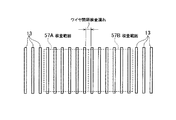
このとき、指令部49で与えられる指示により、例えば、図7に示されているように、一つの視野の検査範囲57Aの右端となる部分と、次に検査される別の視野の検査範囲57Bの左端となる部分は、互いに重複させて検査される。その理由は、図8に示されているように、隣り合う検査範囲57A,57Bの互いに隣り合う端がワイヤ13同士の間隔内に位置した場合は、その箇所の隣り合うワイヤ13同士の間隔の検査漏れが起こるので、この検査漏れを防止するためである。
At this time, according to an instruction given by the
以上のように、ワーク3の全てのワイヤ13が漏れなく検査されるように、上記の検査工程が自動的に繰り返される。
As described above, the above inspection process is automatically repeated so that all the
なお、プリント配線板7の上に異物59があった場合は、撮像した画像が2値化処理されると、図9(A)に示されているように、ワイヤ13以外にも前記異物59が白く見えるために、この2値化処理画像53が膨張処理されると、図9(B)に示されているように、異物59も膨張処理されて異物59の白色面積が大きくなるために、ワイヤ13の部分の白色部分が短絡しているように誤判定され、「不合格」と判定されてしまう可能性がある。
If there is a
そこで、上記の異物59による誤判定を防ぐために、図10(A)に示されているように2値化処理された2値化処理画像53に対しては、一旦、図10(B)に示されているように、前述した収縮処理装置51にて収縮処理を行って異物59の白色部分を画像から除去し、この収縮処理画像61に対して膨張処理を行うことにより、図10(C)に示されているように、ワイヤ13の部分だけが白色に表示された状態で膨張することになる。したがって、この膨張処理画像55に対して、前述したように比較判断装置47により合格、不合格の判定を行うで、誤判定を防止することができる。
Therefore, in order to prevent the erroneous determination by the
以上のように、2値化処理画像53に対して収縮処理と膨張処理を併せて適用することにより、異物59による影響を排除することができる。
As described above, by applying the contraction process and the expansion process to the
また、上記の比較判断装置47により、合格、不合格の判定された画像をメモリ43に記憶する記録工程が行われることが望ましい。すなわち、CCDカメラ19で取得したワイヤ画像、判定に使用した2値化処理後の2値化処理画像53、収縮処理を行った収縮処理画像61、あるいは膨張処理を行った膨張処理画像55の少なくとも一つ以上をメモリ43に記憶して保存することにより、不良調査が可能となる。
In addition, it is desirable that a recording process is performed in which the above-described comparison / determination device 47 stores an image that has been determined to pass or fail in the
なお、前述した実施の形態では、プリント配線板7の回路パターンにおける回路構成部として、隣り合うワイヤ13同士の短絡の検査について説明したが、隣接したボンディング部の短絡の検査も、ワイヤの検査と同様、X−Yステージの上に固定し、CCDカメラの高さを連続的に変化させることでピントを合わせ、ボンディング部に照明を照射して複数個のボンディングを一括で撮像し、ボンディング部のみを2色のうちの一方で表示する2値化処理を行い、必要に応じて膨張及び収縮処理を行い、ボンディング部の色面積を基準値内にあるか否かを判定することで実施可能である。また、ワイヤボンディングに限らずプリント配線板の一般回路についても、同様にX−Yステージの上に固定し、CCDカメラの高さを連続的に変化させることでピントを合わせ、回路部に照明を照射して複数個の回路を一括で撮像し、回路部のみを2色のうちの一方で表示する2値化処理を行い、必要に応じて膨張及び収縮処理を行い、ボンディング部の色面積を基準値内にあるか否かを判定することで実施可能である。
In the above-described embodiment, the inspection of the short circuit between the
以上、説明したように、この発明の実施の形態のプリント配線板の検査方法及びその装置1によれば、撮像手段で撮像した画像に対して2値化処理及び膨張処理の2つの画像処理により、擬似的な短絡も含めたワイヤ短絡の判定検査を、自動的に簡単で正確に、かつ高速に行うことができる。
As described above, according to the printed wiring board inspection method and the
その結果、これまで作業者の目視によって行われていたワイヤボンディングの検査が、画像処理後のワイヤ13の色面積をもとに自動的に実施することができるため、作業者間の判定基準のばらつきや、作業者の体調・疲労などによる不良検出能力のばらつきに影響されることがなく、検査精度が向上する。
As a result, the inspection of wire bonding, which has been performed by visual inspection of the worker so far, can be automatically performed based on the color area of the
さらに、一つの視野で複数本のワイヤ13を同時に検査するので、検査時間の短縮を図ることができる。また、今後、プリント配線板7の配線密度が増大して人間の目視検査に限界が生じる場合においても、CCDカメラ19の画素数を増やすことによって同様に検査することが可能である。
Furthermore, since a plurality of
1 プリント配線板の検査装置
3 ワーク
5 半導体チップ(電子部品)
7 プリント配線板
13 ワイヤ
15 検査エリア
17 X−Yステージ(ワーク載置台)
19 CCDカメラ(撮像手段)
23 制御装置
27 照明装置
29 ステージ移動装置
31 画像処理装置
33 2値化処理装置
35 膨張処理装置
43 メモリ(記憶装置)
45 演算装置
47 比較判断装置
49 指令部
51 収縮処理装置
53 2値化処理画像
55 膨張処理画像
57 検査範囲
59 異物
61 収縮処理画像
1 Printed Wiring
7 Printed
19 CCD camera (imaging means)
23
45 arithmetic unit 47
Claims (14)
検査対象ワークをワーク載置台に固定する工程と、
前記ワークの回路構成部を撮像する撮像手段の位置を連続的に変化させることで前記回路構成部の画像焦点が合う最適な位置を決定する工程と、
前記ワークに照明を照射して前記撮像手段で複数箇所の回路構成部を一括して撮像する工程と、
撮像された画像の回路構成部のみを2色のうちの一方の1色で表示する2値化処理を行う工程と、
前記2値化処理を行った2値化処理画像に対して、基準値以下の回路構成部間距離では回路構成部同士が短絡するまで前記回路構成部を膨張させる膨張処理を行う工程と、
前記膨張処理を行った回路構成部の色面積を取得し、前記色面積が検査合格となる基準値内にあるか否かを判定する工程を実施することを特徴とするプリント配線板の検査方法。 In the method for inspecting a printed wiring board for inspecting the presence or absence of a short circuit in a circuit component in the circuit pattern of the printed wiring board,
A process of fixing a workpiece to be inspected to a workpiece mounting table;
Determining an optimum position at which the image focus of the circuit configuration unit is in focus by continuously changing the position of an imaging unit that images the circuit configuration unit of the workpiece;
Illuminating the workpiece and imaging a plurality of circuit components at the same time with the imaging means; and
Performing a binarization process for displaying only one circuit component of a captured image in one of the two colors;
A step of performing expansion processing for expanding the circuit components until the circuit components are short-circuited at a distance between circuit components equal to or less than a reference value with respect to the binarized image that has been subjected to the binarization processing;
A method for inspecting a printed wiring board, comprising: obtaining a color area of a circuit component that has undergone the expansion process and determining whether the color area is within a reference value that passes the inspection. .
検査対象ワークを固定するワーク載置台と、
前記ワーク載置台の前記ワークの複数箇所の回路構成部を一括して撮像する撮像手段と、
前記撮像手段で撮像した画像に対して前記回路構成部のみを2色のうちの一方の1色で表示する2値化処理を行う2値化処理装置と、
前記2値化処理を行った2値化処理画像に対して、基準値以下の回路構成部間距離では回路構成部同士が短絡するまで前記回路構成部を膨張させる膨張処理を行う膨張処理装置と、
前記膨張処理を行った回路構成部の色面積を計算する演算装置と、この演算装置で計算した前記回路構成部の色面積が検査合格となる基準値内にあるか否かを判定する比較判断装置を備えた制御装置と、で構成されていることを特徴とするプリント配線板の検査装置。 In a printed wiring board inspection device that inspects the presence or absence of a short circuit in a circuit component in the circuit pattern of the printed wiring board,
A workpiece mounting table for fixing the workpiece to be inspected;
Imaging means for collectively imaging a plurality of circuit components of the workpiece on the workpiece mounting table;
A binarization processing device that performs binarization processing for displaying only the circuit configuration unit in one of two colors for an image captured by the imaging unit;
An expansion processing device that performs an expansion process for expanding the circuit components until the circuit components are short-circuited at a distance between circuit components that is equal to or less than a reference value with respect to the binarized image that has been subjected to the binarization process; ,
An arithmetic device that calculates the color area of the circuit component that has undergone the expansion process, and a comparative determination that determines whether or not the color area of the circuit component calculated by the arithmetic device is within a reference value that passes the inspection. A printed wiring board inspection device comprising: a control device including the device.
Priority Applications (1)
| Application Number | Priority Date | Filing Date | Title |
|---|---|---|---|
| JP2008011688A JP5096940B2 (en) | 2008-01-22 | 2008-01-22 | Inspection method and apparatus for printed wiring board |
Applications Claiming Priority (1)
| Application Number | Priority Date | Filing Date | Title |
|---|---|---|---|
| JP2008011688A JP5096940B2 (en) | 2008-01-22 | 2008-01-22 | Inspection method and apparatus for printed wiring board |
Publications (2)
| Publication Number | Publication Date |
|---|---|
| JP2009176826A JP2009176826A (en) | 2009-08-06 |
| JP5096940B2 true JP5096940B2 (en) | 2012-12-12 |
Family
ID=41031643
Family Applications (1)
| Application Number | Title | Priority Date | Filing Date |
|---|---|---|---|
| JP2008011688A Expired - Fee Related JP5096940B2 (en) | 2008-01-22 | 2008-01-22 | Inspection method and apparatus for printed wiring board |
Country Status (1)
| Country | Link |
|---|---|
| JP (1) | JP5096940B2 (en) |
Families Citing this family (1)
| Publication number | Priority date | Publication date | Assignee | Title |
|---|---|---|---|---|
| WO2019082558A1 (en) * | 2017-10-26 | 2019-05-02 | 株式会社新川 | Bonding apparatus |
Family Cites Families (5)
| Publication number | Priority date | Publication date | Assignee | Title |
|---|---|---|---|---|
| JPS61293658A (en) * | 1985-06-21 | 1986-12-24 | Matsushita Electric Works Ltd | Method for inspecting soldering appearance |
| JPH07307371A (en) * | 1994-05-16 | 1995-11-21 | Hitachi Ltd | X-ray inspection device |
| JPH1163932A (en) * | 1997-08-25 | 1999-03-05 | Matsushita Electric Ind Co Ltd | Wire height inspection in wire bonding |
| JP2000012628A (en) * | 1998-06-25 | 2000-01-14 | Nippon Inter Connection Systems Kk | Defect detector for tape carrier, and defect inspection system |
| JP2002076070A (en) * | 2000-08-29 | 2002-03-15 | Mitsubishi Electric Corp | Method and equipment for testing wire bond |
-
2008
- 2008-01-22 JP JP2008011688A patent/JP5096940B2/en not_active Expired - Fee Related
Also Published As
| Publication number | Publication date |
|---|---|
| JP2009176826A (en) | 2009-08-06 |
Similar Documents
| Publication | Publication Date | Title |
|---|---|---|
| JP4946668B2 (en) | Substrate position detection device and substrate position detection method | |
| US7664311B2 (en) | Component mounting board inspecting apparatus | |
| JPH0572961B2 (en) | ||
| TWI483325B (en) | A stitch check device, a probe device and a stitch check method, and a memory medium | |
| JP5096940B2 (en) | Inspection method and apparatus for printed wiring board | |
| JP2004132950A (en) | Appearance inspection apparatus and appearance inspection method | |
| JP2002005850A (en) | Defect inspection method and apparatus therefor, and production method of mask | |
| JP2016070723A (en) | Solder inspection equipment and method | |
| JP2010091360A (en) | Method and device for inspecting image | |
| KR101126759B1 (en) | Method of teaching for electronic parts information in chip mounter | |
| JP7068897B2 (en) | Inspection equipment and inspection method | |
| JP7285988B2 (en) | Inspection device and inspection method | |
| JP2005223006A (en) | Inspection method of cream solder print | |
| JP2006049348A (en) | Method, program, and apparatus for appearance inspection of printed circuit board | |
| JP4220333B2 (en) | Appearance inspection device | |
| JP2008139088A (en) | Visual examination method | |
| JP4087973B2 (en) | Inter-component inspection method and apparatus for mounted components | |
| JP2004085543A (en) | System and method for visual inspection | |
| JP3189604B2 (en) | Inspection method and device | |
| JP2000258353A (en) | Defect inspection method and device | |
| JP2006329679A (en) | Method and device for inspecting product pattern | |
| JP2002296016A (en) | Method for recognizing shape of protective layer of printed circuit board and method of inspection | |
| JP2007147320A (en) | Inspection device | |
| JP2022144974A (en) | Image processing device, image processing method, and inspection device | |
| JP2023053761A (en) | Inspection method and inspection device for electronic component |
Legal Events
| Date | Code | Title | Description |
|---|---|---|---|
| A621 | Written request for application examination |
Free format text: JAPANESE INTERMEDIATE CODE: A621 Effective date: 20101125 |
|
| A977 | Report on retrieval |
Free format text: JAPANESE INTERMEDIATE CODE: A971007 Effective date: 20120823 |
|
| TRDD | Decision of grant or rejection written | ||
| A01 | Written decision to grant a patent or to grant a registration (utility model) |
Free format text: JAPANESE INTERMEDIATE CODE: A01 Effective date: 20120904 |
|
| A01 | Written decision to grant a patent or to grant a registration (utility model) |
Free format text: JAPANESE INTERMEDIATE CODE: A01 |
|
| A61 | First payment of annual fees (during grant procedure) |
Free format text: JAPANESE INTERMEDIATE CODE: A61 Effective date: 20120921 |
|
| FPAY | Renewal fee payment (event date is renewal date of database) |
Free format text: PAYMENT UNTIL: 20150928 Year of fee payment: 3 |
|
| LAPS | Cancellation because of no payment of annual fees |