US7308157B2 - Method and apparatus for optical inspection of a display - Google Patents
Method and apparatus for optical inspection of a display Download PDFInfo
- Publication number
- US7308157B2 US7308157B2 US10/771,126 US77112604A US7308157B2 US 7308157 B2 US7308157 B2 US 7308157B2 US 77112604 A US77112604 A US 77112604A US 7308157 B2 US7308157 B2 US 7308157B2
- Authority
- US
- United States
- Prior art keywords
- image
- pixel
- display
- sensor
- pixels
- Prior art date
- Legal status (The legal status is an assumption and is not a legal conclusion. Google has not performed a legal analysis and makes no representation as to the accuracy of the status listed.)
- Expired - Fee Related, expires
Links
Images


Classifications
-
- G—PHYSICS
- G02—OPTICS
- G02F—OPTICAL DEVICES OR ARRANGEMENTS FOR THE CONTROL OF LIGHT BY MODIFICATION OF THE OPTICAL PROPERTIES OF THE MEDIA OF THE ELEMENTS INVOLVED THEREIN; NON-LINEAR OPTICS; FREQUENCY-CHANGING OF LIGHT; OPTICAL LOGIC ELEMENTS; OPTICAL ANALOGUE/DIGITAL CONVERTERS
- G02F1/00—Devices or arrangements for the control of the intensity, colour, phase, polarisation or direction of light arriving from an independent light source, e.g. switching, gating or modulating; Non-linear optics
- G02F1/01—Devices or arrangements for the control of the intensity, colour, phase, polarisation or direction of light arriving from an independent light source, e.g. switching, gating or modulating; Non-linear optics for the control of the intensity, phase, polarisation or colour
- G02F1/13—Devices or arrangements for the control of the intensity, colour, phase, polarisation or direction of light arriving from an independent light source, e.g. switching, gating or modulating; Non-linear optics for the control of the intensity, phase, polarisation or colour based on liquid crystals, e.g. single liquid crystal display cells
-
- G—PHYSICS
- G06—COMPUTING; CALCULATING OR COUNTING
- G06T—IMAGE DATA PROCESSING OR GENERATION, IN GENERAL
- G06T7/00—Image analysis
- G06T7/0002—Inspection of images, e.g. flaw detection
- G06T7/0004—Industrial image inspection
-
- G—PHYSICS
- G06—COMPUTING; CALCULATING OR COUNTING
- G06F—ELECTRIC DIGITAL DATA PROCESSING
- G06F18/00—Pattern recognition
-
- G—PHYSICS
- G06—COMPUTING; CALCULATING OR COUNTING
- G06T—IMAGE DATA PROCESSING OR GENERATION, IN GENERAL
- G06T2207/00—Indexing scheme for image analysis or image enhancement
- G06T2207/30—Subject of image; Context of image processing
- G06T2207/30108—Industrial image inspection
-
- H—ELECTRICITY
- H04—ELECTRIC COMMUNICATION TECHNIQUE
- H04N—PICTORIAL COMMUNICATION, e.g. TELEVISION
- H04N17/00—Diagnosis, testing or measuring for television systems or their details
- H04N17/02—Diagnosis, testing or measuring for television systems or their details for colour television signals
-
- H—ELECTRICITY
- H04—ELECTRIC COMMUNICATION TECHNIQUE
- H04N—PICTORIAL COMMUNICATION, e.g. TELEVISION
- H04N17/00—Diagnosis, testing or measuring for television systems or their details
- H04N17/04—Diagnosis, testing or measuring for television systems or their details for receivers
Definitions
- the present invention relates to inspection systems. More particularly, the present invention relates to improved optical inspection systems for inspecting flat-panel substrates or displays, such as liquid crystal displays (LCDs).
- LCDs liquid crystal displays
- the '844 patent appears to assume that the panel and camera are perfectly aligned, that is that there is no misalignment angle between them.
- the misalignment angle between the panel and camera is not insignificant.
- typical assembly line positioning systems would be accurate to ⁇ 5 degrees, ⁇ 10 degrees or the like. It would be prohibitively expensive and very time consuming (in the manufacturing line) to have a positioning system that could provide a misalignment accuracy, for example ⁇ 0.01 degrees, small enough so that the misalignment angle could be disregarded. Because typical manufacturing lines do not have such accurate positioning systems, the '844 does not provide a practical solution.
- the '844 patent does not address detection of defective sub-pixels of an LCD pixel, and does not address the detection of defects in portions of sub-pixels of an LCD panel.
- the '844 patent only appears to describe inspecting contrast ratios in LCD pixels.
- manufacturers are concerned with inspecting sup-pixels of a display pixel, for example red, blue, and green sub-pixels. Further, manufacturers are interested in identifying sub-pixels which are partially defective so they can repair the defects.
- a method and apparatus for optically inspecting a display employs sub-pixel accuracy for each primary color to take into account angle of rotation.
- LCDs liquid crystal displays
- optics a small angle of view, flat field of view (FOV), average focus level for all three colors, and four filters (red, green, blue, neutral density);
- sensor array a desired magnification ratio of at least 4 sensor pixels to 1 display pixel, and parallel and independent image capture, processing and analysis;
- image processing coarse detection of candidate defects based on global thresholds on scaled-down or normalized images and fine analysis of the candidate defects based on local thresholds on raw or scaled-down images; color validation: (for sub-pixel and line) based on sub-pixel locations of defects; and dynamic exposure adjustment: addressing within and in-between luminance variations of panels.
- a variety of components which individually contribute to an inspection system and can be variously combined in an inspection system are disclosed herein. This includes: improved optical/sensing configurations including off-axis configuration, XYZ movable configurations, auto-focus cameras with internal filters, and the like; implementations of adaptive scaling algorithms; implementations of background equalization (BGE) and normalization algorithm implementations, and the like.
- improved optical/sensing configurations including off-axis configuration, XYZ movable configurations, auto-focus cameras with internal filters, and the like
- implementations of adaptive scaling algorithms implementations of background equalization (BGE) and normalization algorithm implementations, and the like.
- BGE background equalization
- Quality control of flat-panel displays includes detection and classification of various types of defects. Specifically, defects on LCD panels (both at Cell stage and Module stage) can be categorized into three major groups: high-contrast defects, low-contrast defects and very low-contrast defects.
- the first group of defects consists of RGB sub-pixel (i.e., dot) and RGB line defects.
- the relative-contrast of these defects ranges from full off and on (i.e., stuck-off and stuck-on) to partially off and on (e.g., 1 ⁇ 3 off or 2 ⁇ 3 on). Additionally, such defects might occur as adjacent clusters. For example, a stuck-on red sub-pixel might be located besides a partially green sub-pixel.
- the required information to detect includes exact 2 D location, relative contrast, type of adjacency, etc.
- a second group of defects includes impurities in a panel (which can occur between different layers of a panel: back-light, diffuser film, polarizer films, color filter film, LCD glass, or the like). These defects are typically low-contrast defects. Typically, such defects are small (e.g., less than 16 LCD pixels) and with relative contrast between 4-10% relative to non-defective pixels.
- the required information to detect includes location, size, relative contrast and presence/absence of halo around such defects, and the like.
- the third group of defects consists of very low contrast defects.
- Very-low contrast defects are often called mura defects in the industry (which means stain in Japanese).
- Mura defects can have a wide range of sizes (e.g., from 10 LCD pixels to 100,000 LCD pixels), shapes (e.g., circular, vertical or horizontal narrow and wide lines, spiral form, oblique lines—e.g., rub-lines, random geometrical forms, etc.) and relative-contrast (e.g., as low as 1% to 5-6% relative contrasts).
- Such mura defects often do not have well-defined boundaries.
- the required information of such defects includes location, size, relative contrast, and the like.
- defects such as polarizer scratch, or the like are contemplated. However such type of defects can be typically placed in one of the above groups of defects, along with information such as polarities, brightness, dimness, and the like.
- Embodiments of the present invention include a novel optical/sensing configuration including a multi-camera-system strategy (i.e., an array of cameras) with a very narrow angle of view for each camera.
- a multi-camera-system strategy i.e., an array of cameras
- Moire interference patterns are a periodic modulation of the image voltage signal created by the sensor.
- the period of modulation is a function of the period of the pattern of the sensor pixels and the display pixels.
- the periodic modulation of the image often impedes the ability of an inspection system to detect and characterize real defects that may be present on the flat panel display. The real defects also modulate the signal but tend not be periodic in nature.
- an adaptive scaling algorithm reduces the size of the raw image from a CCD sensor resolution (e.g., 1600 ⁇ 1200) to a scaled-down image resolution (e.g., 400 ⁇ 300 for magnification ratio of 4 CCD pixels to 1 display pixel) increases the gray-level dynamic range (e.g., from 8-bits to ⁇ 12 bits), and compensates for misalignment between the camera sensor pixel array and display panel pixel array.
- inspection and analysis includes the concept of global detection of candidate defects and local analysis of candidate defects. In other words, a global threshold is applied to identify candidate defects in scaled-down images or normalized images; and a localized threshold is applied to perform a fine analysis on the candidate defects in raw images or locally normalized images.
- a method for a computer system includes capturing a plurality of images, a minimal set being a first image and a second image, of a pixel on a display at coordinates (m,n) with an array of R ⁇ S sensors in an image sensor, determining a first and a second set of coordinates on the image sensor that map to coordinates (m,n) on the display for a first and a second group of sub-pixels, respectively, in response to the first and second image, respectively, determining a first and a second misalignment angle between the pixel on the display and the array of R ⁇ S sensors for the first group and the second group of sub-pixels, respectively, and determining an first and a second magnification ratio (x and y) of pixels in the display relative to sensors in the image sensor for the first group and the second group of sub-pixels.
- Steps may also include forming a first and a second reduced scaled image including a plurality of pixels, wherein a luminance value for a pixel at coordinate (m, n) in the first and the second reduced scaled image is determined in response to the first and the second luminance value Imn, respectively, and inspecting the first and the second reduced scaled image to identify potential defects of the pixel on the display.
- an inspection system may include at least one sensor configured to acquire a first and a second image of a portion of a flat-panel display, wherein at least one array of R ⁇ S sensors are configured to capture an image of at least one display pixel in the flat-panel display and a processing unit coupled to at least the one sensor configured to determine a defect in the flat-panel display in response to at least the first and the second image of the portion of the flat-panel display.
- the processing unit typically includes a processor configured to instruct the at least one sensor to capture the first image and the second image of the display pixel with the array of R ⁇ S sensors.
- the processor is also configured to determine a first and second scaled-down image including a plurality of pixels, wherein a luminance value associated with the one display pixel in the first and the second scaled-down image is determined in response to the first and the second luminance value Imn, respectively and is configured to inspect the first and second scaled-down image to identify potential defects of the pixel on the display.
- a method for a computer system may include capturing a first image of at least a portion of a display, wherein an image of a first sub-pixel in a display pixel is captured with an array of sensor pixels in an image sensor, capturing a second image of at least the portion of a display, wherein an image of a second sub-pixel in the display pixel is captured with the array of sensor pixels in the image sensor, determining a first position and a first orientation of the display with respect to the image sensor in response to the first image, and determining a second position and a second orientation of the display with respect to the image sensor in response to the second image.
- additional steps may include for each sensor pixel in the array of sensor pixels, determining a first percentage of overlap of the sensor pixel on top of the display pixel in response to the first position and the first orientation, for each sensor pixel in the array of sensor pixels, determining a second percentage of overlap of the sensor pixel on top of the display pixel in response to the second position and the second orientation, for each sensor pixel in the array of sensor pixels, determining a first intensity value in response to the first image of the display pixel, and for each sensor pixel in the array of sensor pixels, determining a second intensity value in response to the second of the display pixel.
- Additional techniques may include determining a first weighted intensity value associated with the display pixel in response to the first percentage of overlap for each sensor pixel and in response to the first intensity value for each sensor pixel, determining a second weighted intensity value associated with the display pixel in response to the second percentage of overlap for each sensor pixel and in response to the second intensity value for each sensor pixel, forming a first scaled image in response to the first weighted intensity value, and forming a second scaled image in response to the second weighted intensity value.
- the first and the second scaled images may be inspected to determine potential defects in the display.
- FIG. 1 illustrates a block diagram of an inspection system according to one embodiment of the present invention
- FIGS. 2A-C illustrate an embodiment of the present invention
- FIG. 3 illustrates a block diagram of a process flow according to an embodiment of the present invention
- FIG. 4 illustrates a block diagram of a process flow according to an embodiment of the present invention
- FIG. 5 illustrates a block diagram of a process flow according to an embodiment of the present invention
- FIGS. 6A-D illustrate an example of an embodiment of the present invention
- FIGS. 7A-B illustrate a block diagram of a process flow according to an embodiment of the present invention
- FIGS. 8A-B illustrate an example of an embodiment of the present invention.
- FIGS. 9A-B illustrate an example of an embodiment of the present invention.
- FIG. 1 is a block diagram of an inspection system 100 according to an embodiment of the present invention.
- computer system 100 typically includes a monitor 110 , computer 120 , a keyboard and user input device 130 , a network interface, and the like. Additionally, in the present embodiment, computer system 100 may include or may be coupled to one or more image sensors 140 , and a work piece 155 . In additional embodiments, a positioning platform 150 may be provided.
- user input device 130 is typically embodied as a computer mouse, a trackball, a track pad, wireless remote, and the like. Keyboard and user input device 130 typically allows a user to select objects, icons, text, make entries and the like that appear on the monitor 110 .
- Embodiments of a network interface typically include an Ethernet card, a modem (telephone, satellite, cable, ISDN), (asynchronous) digital subscriber line (DSL) unit, and the like.
- a network interface is typically coupled to a computer network as shown.
- a network interface may be physically integrated on the motherboard of computer 120 , may be a software program, such as soft DSL, or the like.
- Computer 120 typically includes familiar computer components such as one or more microprocessors 160 , and memory storage devices, such as a random access memory (RAM) 170 , disk drives 180 , and system bus 190 interconnecting the above components.
- RAM random access memory
- computer 120 is a PC compatible computer having multiple microprocessors such as PentiumIVTM microprocessor from Intel Corporation. In one embodiment, computer 120 includes four to eight processors that operate in parallel. Further, in the present embodiment, computer 120 may include a UNIX-based operating system.
- RAM 170 and disk drive 180 are examples of tangible media for storage of data, audio/video files, computer programs, applet interpreters or compilers, virtual machines, embodiments of the herein described invention including: image data files, defect image data files, adaptive scaling algorithms, background and image equalization algorithms, positioning algorithms for platform 150 , image sensor 140 , and like. Additionally, the tangible media may include image processing algorithms including defect identification algorithms, edge detection algorithms, rotation determination algorithms, and the like. Other types of tangible media include floppy disks, removable hard disks, optical storage media such as CD-ROMS and bar codes, semiconductor memories such as flash memories, read-only-memories (ROMS), battery-backed volatile memories, networked storage devices, and the like.
- computer system 100 may also include software that enables communications over a network such as the HTTP, TCP/IP, RTP/RTSP protocols, and the like.
- software that enables communications over a network
- HTTP HyperText Transfer Protocol
- TCP/IP Transmission Control Protocol
- RTP/RTSP protocols Remote Method Protocol
- other communications software and transfer protocols may also be used, for example IPX, UDP or the like.
- image sensor 140 may include one or more image sensors such as area-scan cameras, CCD cameras, an array of area-scan cameras, or the like. Image sensor 140 may detect various wavelengths of radiation from infrared to ultra violet. In other embodiments, image sensor 140 may detect other types of radiation, such as electron beam back scatter, X-ray emissions, and the like.
- platform 150 allows work piece 155 to be positioned relative to image sensor 140 .
- platform 150 may include x, y, z, and e translation controls, and the like. Using such controls, platform 150 can be used to position work piece 155 relative to image sensor 140 with a high level of accuracy and repeatability.
- work piece 155 can be positioned relative to image sensor 140 with a rotational offset of less than 1/100th of a degree.
- platform 150 may be relatively stationary or have a higher or lower positioning precision than that described above.
- the adaptive scaling algorithm effectively handles misalignment between each sensor, individually, and work piece 155 (e.g. a display).
- FIG. 1 is representative of an inspection system capable of embodying the present invention. It will be readily apparent to one of ordinary skill in the art that additional hardware and software may be added or be removed from FIG. 1 , and still be an embodiment of the present invention contemplated herein. The use of other micro processors are also contemplated, such as PentiumTM or ItaniumTM microprocessors; OpteronTM or AthlonXPTM microprocessors from Advanced Micro Devices, Inc; PowerPC G4TM, G5TM microprocessors from Motorola, Inc.; and the like.
- PentiumTM or ItaniumTM microprocessors such as PentiumTM or ItaniumTM microprocessors; OpteronTM or AthlonXPTM microprocessors from Advanced Micro Devices, Inc; PowerPC G4TM, G5TM microprocessors from Motorola, Inc.; and the like.
- Windows® operating system such as WindowsXP®, WindowsNT®, or the like from Microsoft Corporation
- Solaris from Sun Microsystems
- LINUX Sun Microsystems
- UNIX UNIX
- MAC OS Apple Computer Corporation
- FIG. 2A-C illustrates an embodiment of the present invention. More specifically, FIGS. 2A-C illustrate typical image sensing configurations.
- FIGS. 2A-C illustrate an array of sensors 200 that are adapted to capture images from different portions of a substrate 210 .
- each sensor from array of sensors 200 is a 1600 ⁇ 1200 ⁇ 8 bit CCD (2 megapixel).
- the typical sensor pixel size is 7.4 microns.
- sensors of higher or lower resolution may also be used, and the ratio of horizontal to vertical pixels may be different.
- sensors having 3, 4, 5, 6, etc. mega pixels may be used, and sensors having horizontal to vertical pixels ratios of 1:1, 4:3, 16:9, 1.85:1, or the like may also be used.
- each sensor 200 includes a 77 mm focal length lens (e.g. 35 mm format), although others may also be used. This gives each sensor 200 an angle of view of approximately 8.0 degrees, and the field of view of 105 mm wide. Further, as shown, in the embodiment, sensors 200 are positioned approximately 750 mm from the surface of substrate 210 .
- substrates 210 are liquid crystal displays (LCDs) having resolutions from 1024 ⁇ 768 to 1920 ⁇ 1280. In the future, higher resolution displays, such as 3840 ⁇ 2400 are also contemplated. Additionally, work pieces currently range in size from 15′′ to 56′′ in the diagonal. In the future, sizes of work pieces may be smaller or larger.
- other types of substrates other than LCDs may be inspected with embodiments of the present invention, such as plasma displays, electro luminescent (EL) displays, organic light emitting diode displays (OLEDs), liquid crystal on semiconductor (LCOS), silicon-based displays (e.g. Sony silicon crystal reflective display (SXRD)), or the like.
- an array of sensors 200 is configured to capture images of substrate 210 .
- sixteen sensors 200 are used to capture sixteen different portions of substrate 210 .
- the number of sensors may vary.
- some overlap between images captured by sensors 200 are desirable to cover all display pixels considering the misalignment between sensors, and to ascertain detection of small defects (e.g. spots with 4 ⁇ 4 display pixel area) located in the overlapping areas.
- the images overlap in the x/y directions by approximately 4.5 mm/3.375 mm or approximately 16/12 display pixels; the top and bottom images from sensors 200 extend over the top edge and bottom edge of substrate 210 by approximately 3.375 mm, although these values typically vary.
- substrates 210 include display pixels having red, green, and blue component sub-pixels.
- a color filter assembly 220 e.g. a rotating color wheel
- sensors 200 may be provided in front of sensors 200 .
- Embodiments of the present invention are able to easily handle a range of panel sizes without changing the optical/sensing configuration, and provides a highly orthographic projection of substrate 210 with reduced optical/geometrical distortion. Additionally, such embodiments provide a desirable minimum magnification ratio of 4.0 between the sensor pixels and displays pixels. Accordingly, it enables the system to be able to calculate more accurate coordinates of sub-pixel defects (i.e., a red or green or blue display sub-pixel) and sub-sub-pixel defects (i.e., a portion of a red or green or blue display sub-pixel), stuck-on/stuck-off sub-pixels and line defects, partially dimmer or brighter sub-pixel and line defects, and the like.
- sub-pixel defects i.e., a red or green or blue display sub-pixel
- sub-sub-pixel defects i.e., a portion of a red or green or blue display sub-pixel
- stuck-on/stuck-off sub-pixels and line defects partially
- sensors 200 with auto-focus with internal R/G/B/N filters
- sensors 200 that may be repositioned in x, y, and z, and the like in order to accommodate large range of display sizes and resolutions.
- One desired trait of embodiments of the present invention is to provide a minimum level of image focus. This allows the embodiment to detect very small defects such as R/G/B sub-pixel defects or even sub-sub-pixel R/G/B defects.
- another class of substrate defects can also be detected. This includes defects that are low-contrast, with or without significant off-axis component, that are relatively larger than R/G/B sub-pixel-defect sizes, and the like.
- defects that are low-contrast, with or without significant off-axis component that are relatively larger than R/G/B sub-pixel-defect sizes, and the like.
- focused images are not necessarily required. Accordingly, in such embodiments, any Moire-pattern formed due to a mismatch between sizes of the display pixel and sensor pixel can be reduced by optical smoothing or image processing.
- an on-axis sensor such as sensors 200 and off-axis cameras need not be focused.
- the two classes of substrate defects may be performed by the inclusion of focused on-axis sensor array and not focused off-axis sensors 200 , or on-axis sensors that may be focused and unfocused using their integrated auto-focus mechanisms.
- FIG. 3 illustrates a flow diagram according to an embodiment of the present invention.
- the inspection system is calibrated, step 300 .
- This calibration process is typically performed before initiating image processing functions, described below.
- the off-line calibration includes electronic calibration of each sensor or camera, such as adjusting the camera gain and offset.
- the focus level of each sensor can also be set according to desired focus metric (i.e. focused or defocused.)
- each sensor is then calibrated with respect to luminance ratio.
- This calibration process includes establishing relative Red to White, Green to White and Blue to White luminance ratios for a series of test patterns (e.g. video level 44 of 255, video level 127 of 255, video level 255 of 255, and the like (8-bit).
- the luminance ratios are typically characterized and determined for each flat-panel model and for each sensor.
- this calibration is used to establish an optimal exposure times for Red/Green/Blue color test patterns during on-line testing.
- off-line mechanical x, y and ⁇ adjustments of each individual sensor relative to the work piece are also performed.
- a series of on-line calibration steps are performed, step 310 .
- an optimal exposure time is estimated for various gray-scale test patterns (e.g., RGB uniformly set to gray scale 44 of 255, 127 of 255, and 255 of 255).
- gray-scale test patterns e.g., RGB uniformly set to gray scale 44 of 255, 127 of 255, and 255 of 255.
- the inventors have noted that there is often a significant amount of luminance variation between different flat-panel displays and even often within the same display panel (e.g., between the center and corners).
- an additional function typically performed in step 310 is an (accurate) determination of the position and orientation of each sensor individually, relative to the display panel.
- a number of “offset” and “scaling” parameters are estimated. This includes, a relative offset in the x direction, a relative offset in the y direction, a scale factor in the x direction, a scale factor in the y direction, and an angle, D ⁇ , between the display and each individual sensor.
- the position and orientation vary for each individual color (red, green, blue, white), accordingly, the calibration procedure is performed for each individual sensor for each individual color.
- the determination of the above parameters is typically performed for each color separately: red, green, blue and white due to different refractions of different colors of light through the various optics. More specifically, because the refraction index is different for different colors of light and because the degree of parallelness between each color filter to each CCD sensor is different, the calibration process must be performed separately for each color and each camera. For example, for green test patterns, the calibration pattern consists of green sub-pixel landmarks, and a green filter in front of the sensors. A similar process is performed for blue test patterns, red test patterns, and gray scale test patterns.
- the next step illustrated is capturing, processing, and analyzing data, step 320 .
- this enables the system to, in parallel, capture, process, and analyze data.
- the parallel operation decreases cycle time while capturing and processing/analyzing a significant number of calibration and test patterns (e.g., more than 700 MB of raw image data for each cycle). Additionally, the parallel operation increases inspection throughput. More detailed processes for capturing, processing and analyzing the images will be given below.
- step 330 the next step illustrated in merging of results, step 330 .
- an array of sensors is used to capture the entire display substrate.
- the defect data are merged. This process is called XY Merging.
- a defect that is fully or partially inside overlapped areas of two or more sensors e.g., a gap mura, a vertical/horizontal line mura, or the like
- the average values from the sensors are used for reporting some of defect features (e.g., relative contrast).
- other defect features such as area, bounding box and binary centroid coordinates are recalculated based upon the merged defect data and then reported.
- a Z merging function is performed, where defect data based upon different display patterns are merged together.
- x, y, and z merging may both be used to detect various defects.
- FIG. 4 illustrates a flow diagram according to an embodiment of the present invention. More particularly, FIG. 4 illustrates a process of capturing different display patterns (Test Scenes) displayed on the display substrate with the array of sensors.
- the luminance ratios determined in step 300 , above are provided, 400 .
- the luminance ratios establish a red versus white, green versus white, and blue versus white ratio that is used to adjust the exposure time for red, green, and blue display patterns.
- an estimation of the optimal exposure time for white test patterns, discussed in step 310 , above, is determined, step 410 .
- step 420 the determination of the position and orientation of each sensor, individually, relative to the display panel (mapping calibration) also discussed in step 310 , above is performed, step 420 .
- images of the display are captured with the array of sensors, step 430 .
- the exposure time determined in step 410 is used to set the exposure time.
- step 310 the determination of the position and orientation of the red pixels in the display panel relative to the sensor pixels in each sensor (mapping calibration), also discussed in step 310 , above is performed, step 445 .
- step 310 is typically performed once for r, g, b, and white, and the calibration data is simply retrieved in this step.
- images of red test patterns on the display are captured with the array of sensors, step 450 .
- the exposure time determined in step 410 , and the red to white ratio determined in step 300 is used to set the exposure time.
- steps 445 and 450 are typically repeated with green test scenes and blue test scenes, step 460 .
- a total number of images captured by each camera are at least eighteen “RAW” images.
- a greater or lesser number of images may be captured by other embodiments of the present invention based on engineering considerations and specific processing requirements.
- FIG. 5 illustrates a flow diagram according to an embodiment of the present invention. More particularly, FIG. 5 illustrates a process for processing and analyzing raw, scaled-down, and/or normalized images.
- the captured images are processed with an adaptive scaling process to form a low-resolution image (“scaled-down image”), step 500 , and a normalization process to normalize the image, step 510 . Further details of these processes will be discussed below.
- a design strategy optimization used to facilitate the detection and analysis of defects in an image is by processing both raw images and the scaled-down images. More specifically, global detection of candidate defects are determined from the scaled-down image, and then based upon the candidates, fine local analysis is performed on the raw image or normalized image, depending on defect type. The inventors of the present invention have determined that this coarse to fine processing strategy significantly improves true-defect detection, reduces false-defect rejection, and improves fine-characterization of defects.
- a number of detection and analysis modules, 520 - 580 are provided for identification and analysis of specific types of defects, such as line detection and analysis, impurity/dust detection and analysis, and the like.
- an additional module 590 is provided to identify an edge zone within the image.
- FIGS. 6A-D illustrate embodiments of the present invention. More specifically, FIGS. 6A-D illustrate a number of mapping parameters between the each sensor space and the display panel space. As mentioned in step 310 , above, typical mapping parameters include x and y offsets, x and y scale factors, and a rotation (D ⁇ ).
- a display coordinate frame x, y 600 and a sensor coordinate frame XY 610 are shown.
- a display pixel centered at pixel coordinate (m, n) 620 in coordinate frame 600 is mapped to a sensor pixel coordinate (p, q) 620 in coordinate frame 610 .
- m and n are typically integers whereas p and q are typically floating point numbers.
- the accuracy is to the first decimal place.
- an x offset DX 630 and a y offset DY 640 between the coordinate frames 600 and 610 can be determined.
- a relative rotation D ⁇ 650 between the frames can also be determined by measurement. In one embodiment, the accuracy is to the first decimal place.
- the resolution of the display pixels per unit distance is typically larger than the sensor pixels per unit distance. Accordingly, multiple sensor pixels are adapted to acquire images from a single display pixel.
- the magnification is from 4 to 4.5 sensor pixels per 1 display pixel in at least the x direction. In other embodiments, the magnification ratio may be lesser or greater.
- the magnification may be the same or different in the y direction, depending upon the number of horizontal pixels. In one embodiment including square pixels, the magnification is the same in the horizontal and vertical directions.
- accurate magnification ratios in x and y directions can be calculated for each sensor. In this embodiment, the accuracy for scaling is to the third decimal place.
- the magnification ratios are referred to herein as Pitch_X and Pitch_Y.
- FIG. 6B illustrates an example of a mapping of a grid of display pixels 635 to a grid of sensor pixels 645 when the misalignment angle between the sensor and the display is zero. Such an embodiment is typically rare.
- an R ⁇ S sized kernel 655 of sensor pixels is shown associated with a top-left display pixel 660 .
- the magnification ratio is between approximately 4 to 4.5 between the display pixel and the sensor pixel.
- kernel 655 may be enlarged for example to 7 ⁇ 7 to account for a larger D ⁇ (e.g. >25 degrees) 650 between grid 635 and grid 645 .
- the size of kernel 655 is selected such that a complete display pixel is captured by kernel 655 of sensor pixels.
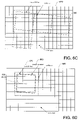
- FIG. 6C illustrates a more typical mapping of a grid of display pixels 665 to a grid of sensor pixels 670 .
- FIG. 6D illustrates another typical mapping of a display pixel 675 to a grid of sensor pixels 680 .
- display pixel 675 is assumed to be rotated around its center point (m,n) 685 and aligned with area 690 .
- the value of D ⁇ is included in the foregoing calculations of weighting values.
- a small D ⁇ is assumed, accordingly the display pixel captured in that figure appears perfect aligned in the x and y direction.
- FIGS. 7A-B illustrate a flow diagram according to an embodiment of the present invention. More particularly, FIGS. 7A-B illustrate a process for adaptively scaling images.
- the mapping parameters are determined between a display grid and a sensor grid, step 700 .
- these parameters include x and y offset, and x and y pitch, and D ⁇ .
- D ⁇ may be larger, as will be illustrated below.
- the mapping is typically performed for each sensor relative to the display substrate, and in response to multiple red, green, blue, and white test scenes.
- DX, DY, Pitch_X, Pitch_Y, and D ⁇ are different for each camera relative to the display substrate. Further, for each sensor, the DX, DY, Pitch_X, Pitch_Y, and D ⁇ parameters may be different for each of the different colored test scenes.
- a display pixel of interest at coordinates (m,n) is mapped to coordinates (p,q) in the sensor grid space, based upon the mapping parameters above, step 710 .
- each sensor pixel in the kernel may capture light emitted from the display pixel, if any.
- each sensor pixel in the kernel may be mapped to at least a portion of the same display pixel, mathematically, a weighting contribution is determined, step 730 .
- the weighting factor is set between 0 and 1, where 0 means that the sensor pixel does not capture any portion of the display pixel and 1 means that the display pixel fully covers the sensor pixel.
- D ⁇ is used to more accurately determine the amount of the display pixel that covers a sensor pixel.
- W ij is a function of D ⁇ is some embodiments. An illustration of this will be given below.
- a total luminance contribution from the display pixel is calculated, step 740 .
- a total luminance value I mn for the display pixel is determine according to the following formula, again where i is a variable that varies from 1 to the number of horizontal sensor pixels R and where j is a variable that varies from 1 to the total number of vertical sensor pixels S in the array of sensor pixels in the kernel.
- the sensor coordinates corresponding to the next display pixel are then calculated, step 755 .
- D ⁇ is measured clock-wise with respect from the x-axis of the sensor grid to the x-axis of the display grid.
- each pixel location (m, n) includes a value Imn, determined above, step 760 .
- This image is referred to above as a “scaled-down” image.
- the image acquired by each sensor was scaled down from the sensor image size to a portion of the display size.
- Each pixel in the scaled down image represents a display pixel and has a higher dynamic range than the sensor image.
- the sensor image is an 8-bit image with pixel resolution of 1600 ⁇ 1200 and the scaled down image is be approximately 400 ⁇ 300 ⁇ 12-bits for magnification ratio of 4.0 or approximately 355 ⁇ 266 ⁇ 12-bits with a magnification ratio of 4.5.
- the system then detects and analyzes the scaled-down image and the original sensor image (RAW image) using one of the analysis modules 520 - 580 . More specifically, in some embodiments, modules use the scaled-down image to identify potential or candidate defects, step 770 . Next, if candidate defects are identified, the original sensor image (RAW image) is processed to determine whether any of the candidate defects are actual defects and/or to determine the characteristics of the defects, step 780 . In other embodiments, modules use a coarse detection strategy based on a global threshold on a normalized image, and use a fine analysis strategy based on a local threshold on a locally normalized image.
- x y merging of defect data is performed, as was described, to determine and/or characterize defects that span more than one sensor image.
- the display may be rejected on the assembly line as being defective, step 790 .
- FIGS. 8A-B illustrates an example according to embodiments of the present invention. More specifically, FIGS. 8A-B illustrate the process of determining an illumination value for the scaled-down image. In this embodiment D ⁇ is ⁇ 10 degrees.
- FIG. 8A Illustrated in FIG. 8A is a grid of sensor pixels 800 and a display pixel 810 .
- display pixel 810 includes red, green, and blue sub pixels, where the green sub-pixel is illuminated at the maximum brightness, in this example 255, and the red and blue sub-pixels are off (e.g. equal to 0).
- a kernel of sensor pixels 820 is illustrated bounding display pixel 810 .
- the weighting values W ij associated with each sensor pixel in kernel 820 is determined. As described above, these values may be determined mathematically based upon relative orientation of sensor pixels 800 and the display panel. Next, as illustrated, luminance values are sensed by each sensor pixel in kernel 820 , as illustrated in array 830 .
- I mn is determined 840 . As illustrated, this value is then used to represent the amount of illumination received from display pixel 810 when the green sub-pixel is fully on.
- the specific value may be scaled up or down according to engineering preference.
- FIGS. 9A-B illustrate examples according to embodiments of the present invention. More specifically, FIGS. 9A-B illustrate an application of the Adaptive Scaling Algorithm to an image from a 15 inch LCD panel.
- Moire pattern artifact noise 910 is clearly visible.
- the Moire pattern noise 920 is also clearly visible in a graph plotting the intensity projections in the X and Y directions for image 900 .
- the Morie noise suppression is also visible in graphs 940 plotting intensity projections in the X and Y directions for image 930 .
- edge pixels of the scaled image are typically darker.
- the point spread function of a display pixel on the sensor pixel has a support base that extends typically more than 10 sensor pixels (i.e., larger than the magnification ratio of the optical system used, that is, 4 to 4.5). Accordingly, when the scaling algorithm described above is applied to edge pixels in the display, the total integrated energy is smaller than for display pixels that are not located at the edge of the panel. During the detection and analysis process, edge pixels are thus processed using different parameters.
- the edge pixel issue is typically more apparent on the left and right sides of the display panel than on the top and bottom sides. This is typically due to the difference in the sampling frequency of a sub-pixel (Red, Green or Blue). For example, for a magnification ratio of 4 to 1, the sampling frequency of a sub-pixel along Y-axis is 4 to 1 whereas along X-axis the sampling frequency is 1.33 to 1.
- image sensors may be optical detectors such as CCD cameras, CMOS-based cameras, or the like; the image sensors may detect back-scatter radiation, for example as used in scanning electron microscopes, and the like; or the like.
- the adaptive scaling process described may be modified.
- the magnification between the display pixel and sensor pixel may be increased, for example to obtain a magnification ration of 5 to 1 or 6 to 1 or greater in the x direction.
- weighting factors may also depend upon the position of the sensor pixel within the kernel. For example, when inspecting for red sub-pixel defects, those sensor pixels on the left side of the kernel may be weighted more than the sensor pixels on the right side of the kernel.
- the integral of the luminance may also have a linear or non-linear relationship.
- the compensation of the angle between the display grid and the sensor grid may be performed in different ways, for example, by not assuming that each individual display pixel is square relative to the sensor pixels when determining the total luminance of the display pixel.
Abstract
Description
I mn=Σ(W ij *L ij) for i=1 to R, and j=1 to S
X(1)=X(0)+Pitch— X*Cos(Dθ);
Y(1)=Y(0)+Pitch— Y*Sin(Dθ)
X(1)=X(0)−Pitch— X*Sin(Dθ);
Y(1)=Y(0)+Pitch— Y*Cos (Dθ)
Claims (20)
Priority Applications (1)
| Application Number | Priority Date | Filing Date | Title |
|---|---|---|---|
| US10/771,126 US7308157B2 (en) | 2003-02-03 | 2004-02-02 | Method and apparatus for optical inspection of a display |
Applications Claiming Priority (2)
| Application Number | Priority Date | Filing Date | Title |
|---|---|---|---|
| US44488903P | 2003-02-03 | 2003-02-03 | |
| US10/771,126 US7308157B2 (en) | 2003-02-03 | 2004-02-02 | Method and apparatus for optical inspection of a display |
Publications (2)
| Publication Number | Publication Date |
|---|---|
| US20040213449A1 US20040213449A1 (en) | 2004-10-28 |
| US7308157B2 true US7308157B2 (en) | 2007-12-11 |
Family
ID=32850948
Family Applications (1)
| Application Number | Title | Priority Date | Filing Date |
|---|---|---|---|
| US10/771,126 Expired - Fee Related US7308157B2 (en) | 2003-02-03 | 2004-02-02 | Method and apparatus for optical inspection of a display |
Country Status (6)
| Country | Link |
|---|---|
| US (1) | US7308157B2 (en) |
| JP (1) | JP2006520482A (en) |
| KR (1) | KR100983943B1 (en) |
| CN (1) | CN100367293C (en) |
| TW (1) | TWI236840B (en) |
| WO (1) | WO2004070693A2 (en) |
Cited By (9)
| Publication number | Priority date | Publication date | Assignee | Title |
|---|---|---|---|---|
| US20050232476A1 (en) * | 2004-04-19 | 2005-10-20 | Semiconductor Energy Laboratory Co., Ltd. | Image analysis method, image analysis program and pixel evaluation system having the sames |
| US20070291189A1 (en) * | 2006-06-16 | 2007-12-20 | Michael Harville | Blend maps for rendering an image frame |
| US20080063254A1 (en) * | 2006-09-07 | 2008-03-13 | Kabushiki Kaisha Toshiba | Unevenness inspection method, method for manufacturing display panel, and unevenness inspection apparatus |
| US7854518B2 (en) * | 2006-06-16 | 2010-12-21 | Hewlett-Packard Development Company, L.P. | Mesh for rendering an image frame |
| US20110211750A1 (en) * | 2010-02-26 | 2011-09-01 | Sony Corporation | Method and apparatus for determining misalignment |
| US8328365B2 (en) | 2009-04-30 | 2012-12-11 | Hewlett-Packard Development Company, L.P. | Mesh for mapping domains based on regularized fiducial marks |
| US8976250B2 (en) | 2012-05-01 | 2015-03-10 | Apple Inc. | Lens inspection system |
| US9035673B2 (en) | 2010-01-25 | 2015-05-19 | Palo Alto Research Center Incorporated | Method of in-process intralayer yield detection, interlayer shunt detection and correction |
| WO2016207703A1 (en) | 2015-06-23 | 2016-12-29 | Bosch Car Multimedia Portugal, S.A. | Apparatus and method for detection of pixel or sub-pixel functional defects of an image display |
Families Citing this family (136)
| Publication number | Priority date | Publication date | Assignee | Title |
|---|---|---|---|---|
| US6950115B2 (en) | 2001-05-09 | 2005-09-27 | Clairvoyante, Inc. | Color flat panel display sub-pixel arrangements and layouts |
| US7417648B2 (en) | 2002-01-07 | 2008-08-26 | Samsung Electronics Co. Ltd., | Color flat panel display sub-pixel arrangements and layouts for sub-pixel rendering with split blue sub-pixels |
| US20040051724A1 (en) | 2002-09-13 | 2004-03-18 | Elliott Candice Hellen Brown | Four color arrangements of emitters for subpixel rendering |
| US7167186B2 (en) | 2003-03-04 | 2007-01-23 | Clairvoyante, Inc | Systems and methods for motion adaptive filtering |
| US7352374B2 (en) | 2003-04-07 | 2008-04-01 | Clairvoyante, Inc | Image data set with embedded pre-subpixel rendered image |
| US8035599B2 (en) | 2003-06-06 | 2011-10-11 | Samsung Electronics Co., Ltd. | Display panel having crossover connections effecting dot inversion |
| US7397455B2 (en) | 2003-06-06 | 2008-07-08 | Samsung Electronics Co., Ltd. | Liquid crystal display backplane layouts and addressing for non-standard subpixel arrangements |
| US20040246280A1 (en) | 2003-06-06 | 2004-12-09 | Credelle Thomas Lloyd | Image degradation correction in novel liquid crystal displays |
| US7084923B2 (en) | 2003-10-28 | 2006-08-01 | Clairvoyante, Inc | Display system having improved multiple modes for displaying image data from multiple input source formats |
| US7525526B2 (en) * | 2003-10-28 | 2009-04-28 | Samsung Electronics Co., Ltd. | System and method for performing image reconstruction and subpixel rendering to effect scaling for multi-mode display |
| JP4845382B2 (en) * | 2004-02-06 | 2011-12-28 | キヤノン株式会社 | Image processing apparatus, control method therefor, computer program, and computer-readable storage medium |
| JP4480002B2 (en) * | 2004-05-28 | 2010-06-16 | Hoya株式会社 | Nonuniformity defect inspection method and apparatus, and photomask manufacturing method |
| US20060061248A1 (en) * | 2004-09-22 | 2006-03-23 | Eastman Kodak Company | Uniformity and brightness measurement in OLED displays |
| KR100769428B1 (en) * | 2005-04-28 | 2007-10-22 | 삼성에스디아이 주식회사 | Light emitting display, and apparatus and method for digitizing brightness thereof |
| US7364306B2 (en) | 2005-06-20 | 2008-04-29 | Digital Display Innovations, Llc | Field sequential light source modulation for a digital display system |
| US7404645B2 (en) * | 2005-06-20 | 2008-07-29 | Digital Display Innovations, Llc | Image and light source modulation for a digital display system |
| EP1739443A1 (en) * | 2005-06-29 | 2007-01-03 | SwissQual License AG | A device and method for assessing the quality of a mobile phone or mobile phone network |
| WO2007047685A2 (en) * | 2005-10-17 | 2007-04-26 | I2Ic Corporation | Combined video display and camera system |
| WO2007094627A1 (en) * | 2006-02-15 | 2007-08-23 | Dongjin Semichem Co., Ltd | System for testing a flat panel display device and method thereof |
| KR100834730B1 (en) * | 2006-09-04 | 2008-06-05 | 케이 이엔지(주) | Inspection system of inferior liquid crystal display panel using vision sensor |
| EP2147296A1 (en) * | 2007-04-18 | 2010-01-27 | Micronic Laser Systems Ab | Method and apparatus for mura detection and metrology |
| US8049695B2 (en) * | 2007-10-15 | 2011-11-01 | Sharp Laboratories Of America, Inc. | Correction of visible mura distortions in displays by use of flexible system for memory resources and mura characteristics |
| US20090175530A1 (en) * | 2007-11-12 | 2009-07-09 | Fredrik Sjostrom | Methods and apparatuses for detecting pattern errors |
| KR101101132B1 (en) * | 2007-11-23 | 2012-01-12 | 삼성엘이디 주식회사 | LED inspection apparatus and inspection method using the same |
| IL188825A0 (en) * | 2008-01-16 | 2008-11-03 | Orbotech Ltd | Inspection of a substrate using multiple cameras |
| US8902321B2 (en) | 2008-05-20 | 2014-12-02 | Pelican Imaging Corporation | Capturing and processing of images using monolithic camera array with heterogeneous imagers |
| US8866920B2 (en) | 2008-05-20 | 2014-10-21 | Pelican Imaging Corporation | Capturing and processing of images using monolithic camera array with heterogeneous imagers |
| US11792538B2 (en) | 2008-05-20 | 2023-10-17 | Adeia Imaging Llc | Capturing and processing of images including occlusions focused on an image sensor by a lens stack array |
| JP5286938B2 (en) * | 2008-05-27 | 2013-09-11 | 東京エレクトロン株式会社 | Needle mark inspection device, probe device, needle mark inspection method, and storage medium |
| KR100910175B1 (en) * | 2009-04-06 | 2009-07-30 | (주)에이직뱅크 | Image sensor for generating a three dimensional image |
| US8508507B2 (en) * | 2009-04-08 | 2013-08-13 | Integrated Digital Technologies, Inc. | Input detection systems and methods for display panels with embedded photo sensors |
| US8514491B2 (en) | 2009-11-20 | 2013-08-20 | Pelican Imaging Corporation | Capturing and processing of images using monolithic camera array with heterogeneous imagers |
| SG10201503516VA (en) | 2010-05-12 | 2015-06-29 | Pelican Imaging Corp | Architectures for imager arrays and array cameras |
| WO2011151866A1 (en) * | 2010-06-04 | 2011-12-08 | パナソニック株式会社 | Method for measuring brightness of light-emitting display panel |
| US8380845B2 (en) | 2010-10-08 | 2013-02-19 | Microsoft Corporation | Providing a monitoring service in a cloud-based computing environment |
| US8959219B2 (en) | 2010-10-18 | 2015-02-17 | Microsoft Technology Licensing, Llc | Dynamic rerouting of service requests between service endpoints for web services in a composite service |
| US8874787B2 (en) | 2010-10-20 | 2014-10-28 | Microsoft Corporation | Optimized consumption of third-party web services in a composite service |
| US8878950B2 (en) | 2010-12-14 | 2014-11-04 | Pelican Imaging Corporation | Systems and methods for synthesizing high resolution images using super-resolution processes |
| US9970180B2 (en) * | 2011-03-14 | 2018-05-15 | Caterpillar Trimble Control Technologies Llc | System for machine control |
| CN103765864B (en) | 2011-05-11 | 2017-07-04 | 派力肯影像公司 | For transmitting the system and method with receiving array camera image data |
| US8866899B2 (en) * | 2011-06-07 | 2014-10-21 | Photon Dynamics Inc. | Systems and methods for defect detection using a whole raw image |
| WO2013003276A1 (en) | 2011-06-28 | 2013-01-03 | Pelican Imaging Corporation | Optical arrangements for use with an array camera |
| US20130265459A1 (en) | 2011-06-28 | 2013-10-10 | Pelican Imaging Corporation | Optical arrangements for use with an array camera |
| US8704895B2 (en) * | 2011-08-29 | 2014-04-22 | Qualcomm Incorporated | Fast calibration of displays using spectral-based colorimetrically calibrated multicolor camera |
| WO2013043761A1 (en) | 2011-09-19 | 2013-03-28 | Pelican Imaging Corporation | Determining depth from multiple views of a scene that include aliasing using hypothesized fusion |
| US9129183B2 (en) | 2011-09-28 | 2015-09-08 | Pelican Imaging Corporation | Systems and methods for encoding light field image files |
| KR101189209B1 (en) * | 2011-10-06 | 2012-10-09 | 늘솜주식회사 | Position recognizing apparatus and methed therefor |
| JP2013160629A (en) * | 2012-02-06 | 2013-08-19 | Hitachi High-Technologies Corp | Defect inspection method, defect inspection apparatus, program, and output unit |
| EP2817955B1 (en) | 2012-02-21 | 2018-04-11 | FotoNation Cayman Limited | Systems and methods for the manipulation of captured light field image data |
| US9210392B2 (en) | 2012-05-01 | 2015-12-08 | Pelican Imaging Coporation | Camera modules patterned with pi filter groups |
| CN104508681B (en) | 2012-06-28 | 2018-10-30 | Fotonation开曼有限公司 | For detecting defective camera array, optical device array and the system and method for sensor |
| US20140002674A1 (en) | 2012-06-30 | 2014-01-02 | Pelican Imaging Corporation | Systems and Methods for Manufacturing Camera Modules Using Active Alignment of Lens Stack Arrays and Sensors |
| KR101996917B1 (en) | 2012-07-20 | 2019-10-02 | 삼성디스플레이 주식회사 | Method and apparatus for inspecting flat panel display |
| CN104662589B (en) | 2012-08-21 | 2017-08-04 | 派力肯影像公司 | For the parallax detection in the image using array camera seizure and the system and method for correction |
| US20140055632A1 (en) | 2012-08-23 | 2014-02-27 | Pelican Imaging Corporation | Feature based high resolution motion estimation from low resolution images captured using an array source |
| WO2014043641A1 (en) | 2012-09-14 | 2014-03-20 | Pelican Imaging Corporation | Systems and methods for correcting user identified artifacts in light field images |
| EP4307659A1 (en) | 2012-09-28 | 2024-01-17 | Adeia Imaging LLC | Generating images from light fields utilizing virtual viewpoints |
| WO2014078443A1 (en) | 2012-11-13 | 2014-05-22 | Pelican Imaging Corporation | Systems and methods for array camera focal plane control |
| TWI512277B (en) * | 2013-01-04 | 2015-12-11 | Taiwan Power Testing Technology Co Ltd | Monitor inspection equipment |
| KR20200067917A (en) * | 2013-02-18 | 2020-06-12 | 카티바, 인크. | Systems, devices and methods for the quality assessment of oled stack films |
| US9462164B2 (en) | 2013-02-21 | 2016-10-04 | Pelican Imaging Corporation | Systems and methods for generating compressed light field representation data using captured light fields, array geometry, and parallax information |
| WO2014133974A1 (en) | 2013-02-24 | 2014-09-04 | Pelican Imaging Corporation | Thin form computational and modular array cameras |
| US9638883B1 (en) | 2013-03-04 | 2017-05-02 | Fotonation Cayman Limited | Passive alignment of array camera modules constructed from lens stack arrays and sensors based upon alignment information obtained during manufacture of array camera modules using an active alignment process |
| WO2014138695A1 (en) | 2013-03-08 | 2014-09-12 | Pelican Imaging Corporation | Systems and methods for measuring scene information while capturing images using array cameras |
| US8866912B2 (en) * | 2013-03-10 | 2014-10-21 | Pelican Imaging Corporation | System and methods for calibration of an array camera using a single captured image |
| US9521416B1 (en) | 2013-03-11 | 2016-12-13 | Kip Peli P1 Lp | Systems and methods for image data compression |
| EP2972589B1 (en) | 2013-03-12 | 2017-05-03 | Micronic Mydata AB | Mechanically produced alignment fiducial method and alignment system |
| WO2014140047A2 (en) | 2013-03-12 | 2014-09-18 | Micronic Mydata AB | Method and device for writing photomasks with reduced mura errors |
| US9106784B2 (en) | 2013-03-13 | 2015-08-11 | Pelican Imaging Corporation | Systems and methods for controlling aliasing in images captured by an array camera for use in super-resolution processing |
| WO2014164909A1 (en) | 2013-03-13 | 2014-10-09 | Pelican Imaging Corporation | Array camera architecture implementing quantum film sensors |
| US9519972B2 (en) | 2013-03-13 | 2016-12-13 | Kip Peli P1 Lp | Systems and methods for synthesizing images from image data captured by an array camera using restricted depth of field depth maps in which depth estimation precision varies |
| US9124831B2 (en) | 2013-03-13 | 2015-09-01 | Pelican Imaging Corporation | System and methods for calibration of an array camera |
| US9578259B2 (en) | 2013-03-14 | 2017-02-21 | Fotonation Cayman Limited | Systems and methods for reducing motion blur in images or video in ultra low light with array cameras |
| US8836797B1 (en) * | 2013-03-14 | 2014-09-16 | Radiant-Zemax Holdings, LLC | Methods and systems for measuring and correcting electronic visual displays |
| US9100586B2 (en) | 2013-03-14 | 2015-08-04 | Pelican Imaging Corporation | Systems and methods for photometric normalization in array cameras |
| US9445003B1 (en) | 2013-03-15 | 2016-09-13 | Pelican Imaging Corporation | Systems and methods for synthesizing high resolution images using image deconvolution based on motion and depth information |
| US9438888B2 (en) | 2013-03-15 | 2016-09-06 | Pelican Imaging Corporation | Systems and methods for stereo imaging with camera arrays |
| US9633442B2 (en) | 2013-03-15 | 2017-04-25 | Fotonation Cayman Limited | Array cameras including an array camera module augmented with a separate camera |
| US9497429B2 (en) | 2013-03-15 | 2016-11-15 | Pelican Imaging Corporation | Extended color processing on pelican array cameras |
| US10122993B2 (en) | 2013-03-15 | 2018-11-06 | Fotonation Limited | Autofocus system for a conventional camera that uses depth information from an array camera |
| US9497370B2 (en) | 2013-03-15 | 2016-11-15 | Pelican Imaging Corporation | Array camera architecture implementing quantum dot color filters |
| CN103440654B (en) * | 2013-08-27 | 2016-08-10 | 南京大学 | A kind of LCD foreign body defect detection method |
| US9898856B2 (en) | 2013-09-27 | 2018-02-20 | Fotonation Cayman Limited | Systems and methods for depth-assisted perspective distortion correction |
| WO2015070105A1 (en) | 2013-11-07 | 2015-05-14 | Pelican Imaging Corporation | Methods of manufacturing array camera modules incorporating independently aligned lens stacks |
| US10119808B2 (en) | 2013-11-18 | 2018-11-06 | Fotonation Limited | Systems and methods for estimating depth from projected texture using camera arrays |
| EP3075140B1 (en) | 2013-11-26 | 2018-06-13 | FotoNation Cayman Limited | Array camera configurations incorporating multiple constituent array cameras |
| KR102175702B1 (en) * | 2013-12-30 | 2020-11-09 | 삼성디스플레이 주식회사 | Method of compensating mura of display apparatus and vision inspection apparatus performing the method |
| US10089740B2 (en) | 2014-03-07 | 2018-10-02 | Fotonation Limited | System and methods for depth regularization and semiautomatic interactive matting using RGB-D images |
| US9247117B2 (en) | 2014-04-07 | 2016-01-26 | Pelican Imaging Corporation | Systems and methods for correcting for warpage of a sensor array in an array camera module by introducing warpage into a focal plane of a lens stack array |
| US9521319B2 (en) | 2014-06-18 | 2016-12-13 | Pelican Imaging Corporation | Array cameras and array camera modules including spectral filters disposed outside of a constituent image sensor |
| EP3467776A1 (en) | 2014-09-29 | 2019-04-10 | Fotonation Cayman Limited | Systems and methods for dynamic calibration of array cameras |
| KR102248789B1 (en) * | 2014-10-07 | 2021-05-06 | 삼성전자 주식회사 | Application processor for sharing resource based on image resolution and devices having same |
| CN104317079B (en) * | 2014-10-29 | 2017-12-01 | 京东方科技集团股份有限公司 | A kind of display panel identifying system, detecting system, recognition methods and detection method |
| CN105704482A (en) * | 2014-11-27 | 2016-06-22 | 英业达科技有限公司 | Screen detection method |
| US20160292376A1 (en) * | 2015-04-02 | 2016-10-06 | Advan Int'l Corp. | Method for calibrating medical display device using smartphone |
| US9942474B2 (en) | 2015-04-17 | 2018-04-10 | Fotonation Cayman Limited | Systems and methods for performing high speed video capture and depth estimation using array cameras |
| CN104914133B (en) * | 2015-06-19 | 2017-12-22 | 合肥京东方光电科技有限公司 | Rub defect detecting device |
| KR102409966B1 (en) * | 2015-09-17 | 2022-06-16 | 삼성전자주식회사 | Method of manufacturing light source module |
| CN105204195B (en) * | 2015-09-21 | 2018-05-25 | 京东方科技集团股份有限公司 | A kind of liquid crystal panel detects integrated system into box |
| EP3356865A4 (en) | 2015-10-02 | 2019-06-12 | Aptiv Technologies Limited | Method and system using refractive beam mapper to reduce moiré interference in a display system including multiple displays |
| WO2017056058A1 (en) | 2015-10-02 | 2017-04-06 | Pure Depth Limited | Method and system for performing color filter offsets in order to reduce moiré interference in a display system including multiple displays |
| US10379370B2 (en) | 2015-10-02 | 2019-08-13 | Pure Depth Limited | Method and system for performing sub-pixel compression in order to reduce moire interference in a display system including multiple displays |
| AU2016349895B2 (en) * | 2015-11-04 | 2022-01-13 | Magic Leap, Inc. | Light field display metrology |
| CN105426926B (en) * | 2016-01-04 | 2019-09-24 | 京东方科技集团股份有限公司 | A kind of couple of AMOLED carries out the method and device of detection classification |
| CN107155058B (en) * | 2016-03-02 | 2020-04-21 | 由田新技股份有限公司 | Object automatic correction method and automatic correction detection device thereof |
| TWI603060B (en) * | 2016-03-02 | 2017-10-21 | 由田新技股份有限公司 | Automatic object alignment method and automatic alignment inspection device thereof |
| US10181391B2 (en) | 2016-05-26 | 2019-01-15 | Nanojehm Inc. | Image processing system and method of processing images |
| US10366674B1 (en) | 2016-12-27 | 2019-07-30 | Facebook Technologies, Llc | Display calibration in electronic displays |
| US10311276B2 (en) * | 2017-02-22 | 2019-06-04 | Synaptics Incorporated | Under display optical fingerprint sensor arrangement for mitigating moiré effects |
| US10482618B2 (en) | 2017-08-21 | 2019-11-19 | Fotonation Limited | Systems and methods for hybrid depth regularization |
| WO2019040310A1 (en) * | 2017-08-24 | 2019-02-28 | Radiant Vision Systems, LLC | Methods and systems for measuring electronic visual displays using fractional pixels |
| CN108022266B (en) * | 2017-12-14 | 2024-02-02 | 杭州电子科技大学 | Artificial intelligent image recognition method for photovoltaic cell on-line position detection |
| CN108303424A (en) * | 2018-01-02 | 2018-07-20 | 京东方科技集团股份有限公司 | Display panel testing and its detection method |
| US10755133B2 (en) * | 2018-02-22 | 2020-08-25 | Samsung Display Co., Ltd. | System and method for line Mura detection with preprocessing |
| TWI672493B (en) * | 2018-03-07 | 2019-09-21 | 由田新技股份有限公司 | An automatic optical inspection system and method to obtain mura defect from the panel |
| CN109141822B (en) * | 2018-08-02 | 2020-07-03 | 凌云光技术集团有限责任公司 | Screen defect detection device and method based on four-piece type color filter |
| CN109164551A (en) * | 2018-10-25 | 2019-01-08 | 苏州源泽光电科技集团有限公司 | A kind of optical lens detected for showing screen |
| KR20200074299A (en) * | 2018-12-14 | 2020-06-25 | 삼성디스플레이 주식회사 | Vision inspection apparatus and method of driving the same |
| CN109727233B (en) * | 2018-12-18 | 2021-06-08 | 武汉精立电子技术有限公司 | LCD defect detection method |
| KR20200081541A (en) * | 2018-12-27 | 2020-07-08 | 삼성디스플레이 주식회사 | Imaging apparatus and driving method of the same |
| TWI693386B (en) * | 2019-05-09 | 2020-05-11 | 聯策科技股份有限公司 | System and method for optimally adjusting imaging parameters |
| US10825163B1 (en) | 2019-06-13 | 2020-11-03 | Viavi Solutions Inc. | Automatically executing a test to inspect an end face of an optical fiber when an image is in focus |
| DE112020004391T5 (en) | 2019-09-17 | 2022-06-02 | Boston Polarimetrics, Inc. | SYSTEMS AND METHODS FOR SURFACE MODELING USING POLARIZATION FEATURES |
| WO2021071995A1 (en) | 2019-10-07 | 2021-04-15 | Boston Polarimetrics, Inc. | Systems and methods for surface normals sensing with polarization |
| CA3162710A1 (en) | 2019-11-30 | 2021-06-03 | Boston Polarimetrics, Inc. | Systems and methods for transparent object segmentation using polarization cues |
| KR20220132620A (en) | 2020-01-29 | 2022-09-30 | 인트린식 이노베이션 엘엘씨 | Systems and methods for characterizing object pose detection and measurement systems |
| KR20220133973A (en) | 2020-01-30 | 2022-10-05 | 인트린식 이노베이션 엘엘씨 | Systems and methods for synthesizing data to train statistical models for different imaging modalities, including polarized images |
| KR102355463B1 (en) * | 2020-03-27 | 2022-01-26 | 하이버스 주식회사 | System and Method for Inspecting Display Panel |
| KR102355462B1 (en) * | 2020-03-27 | 2022-01-26 | 하이버스 주식회사 | System for Inspecting Display Panel |
| US11953700B2 (en) | 2020-05-27 | 2024-04-09 | Intrinsic Innovation Llc | Multi-aperture polarization optical systems using beam splitters |
| US11954886B2 (en) | 2021-04-15 | 2024-04-09 | Intrinsic Innovation Llc | Systems and methods for six-degree of freedom pose estimation of deformable objects |
| US11290658B1 (en) | 2021-04-15 | 2022-03-29 | Boston Polarimetrics, Inc. | Systems and methods for camera exposure control |
| DE102021205703A1 (en) | 2021-06-07 | 2022-12-08 | TechnoTeam Holding GmbH | Method and device for photometric measurement of an electronic display and method for controlling an electronic display |
| US11689813B2 (en) | 2021-07-01 | 2023-06-27 | Intrinsic Innovation Llc | Systems and methods for high dynamic range imaging using crossed polarizers |
| KR102560720B1 (en) * | 2022-06-08 | 2023-07-28 | 시냅스이미징(주) | Inspection apparatus for substrate having multiple inspection units |
| KR20240022084A (en) * | 2022-08-11 | 2024-02-20 | 주식회사 엘엑스세미콘 | Apparatus and Method for Compensating Mura |
Citations (11)
| Publication number | Priority date | Publication date | Assignee | Title |
|---|---|---|---|---|
| US5418371A (en) | 1993-02-01 | 1995-05-23 | Aslund; Nils R. D. | Apparatus for quantitative imaging of multiple fluorophores using dual detectors |
| US5650844A (en) | 1994-07-14 | 1997-07-22 | Advantest Corporation | LCD panel image quality inspection system and LCD image presampling method |
| US5703362A (en) * | 1996-01-02 | 1997-12-30 | General Electric Company | Method for nondestructive/noncontact detection and quantification of alpha case on a surface of a workpiece made of titanium or a titanium-based alloy |
| US6166366A (en) * | 1997-07-23 | 2000-12-26 | Cc1, Inc. | System and method for monitoring and controlling the deposition of pattern and overall material coatings |
| US6177955B1 (en) | 1997-10-09 | 2001-01-23 | Westar Corporation | Visual display inspection system |
| US6266437B1 (en) * | 1998-09-04 | 2001-07-24 | Sandia Corporation | Sequential detection of web defects |
| US6323922B1 (en) | 1994-04-19 | 2001-11-27 | Nec Corporation | Liquid crystal display cell |
| US20020075439A1 (en) | 2000-10-31 | 2002-06-20 | Hideki Uehara | Electro-optical device, inspection method therefor, and electronic equipment |
| US6504943B1 (en) * | 1998-07-20 | 2003-01-07 | Sandia Corporation | Information-efficient spectral imaging sensor |
| US6531707B1 (en) | 2000-12-29 | 2003-03-11 | Cognex Corporation | Machine vision method for the inspection of a material for defects |
| US6874420B2 (en) * | 1999-10-22 | 2005-04-05 | Cc1, Inc. | System and method for register mark recognition |
Family Cites Families (5)
| Publication number | Priority date | Publication date | Assignee | Title |
|---|---|---|---|---|
| JP2766942B2 (en) * | 1991-02-04 | 1998-06-18 | ミナトエレクトロニクス 株式会社 | Display screen reading method of display element |
| JPH06250139A (en) * | 1993-02-23 | 1994-09-09 | Casio Comput Co Ltd | Method for inspecting liquid crystal display pannel |
| JP3087098B2 (en) * | 1993-02-23 | 2000-09-11 | カシオ計算機株式会社 | Method for detecting position and rotation angle of display pixel of liquid crystal display panel |
| JP3343445B2 (en) * | 1994-07-14 | 2002-11-11 | 株式会社アドバンテスト | LCD panel image quality inspection system |
| JP3512535B2 (en) * | 1995-05-19 | 2004-03-29 | 株式会社アドバンテスト | Panel image quality inspection apparatus and image quality correction method thereof |
-
2004
- 2004-02-02 US US10/771,126 patent/US7308157B2/en not_active Expired - Fee Related
- 2004-02-03 TW TW093102377A patent/TWI236840B/en not_active IP Right Cessation
- 2004-02-03 KR KR1020057014221A patent/KR100983943B1/en not_active IP Right Cessation
- 2004-02-03 WO PCT/US2004/003217 patent/WO2004070693A2/en active Application Filing
- 2004-02-03 JP JP2006503322A patent/JP2006520482A/en active Pending
- 2004-02-03 CN CNB2004800034163A patent/CN100367293C/en not_active Expired - Fee Related
Patent Citations (11)
| Publication number | Priority date | Publication date | Assignee | Title |
|---|---|---|---|---|
| US5418371A (en) | 1993-02-01 | 1995-05-23 | Aslund; Nils R. D. | Apparatus for quantitative imaging of multiple fluorophores using dual detectors |
| US6323922B1 (en) | 1994-04-19 | 2001-11-27 | Nec Corporation | Liquid crystal display cell |
| US5650844A (en) | 1994-07-14 | 1997-07-22 | Advantest Corporation | LCD panel image quality inspection system and LCD image presampling method |
| US5703362A (en) * | 1996-01-02 | 1997-12-30 | General Electric Company | Method for nondestructive/noncontact detection and quantification of alpha case on a surface of a workpiece made of titanium or a titanium-based alloy |
| US6166366A (en) * | 1997-07-23 | 2000-12-26 | Cc1, Inc. | System and method for monitoring and controlling the deposition of pattern and overall material coatings |
| US6177955B1 (en) | 1997-10-09 | 2001-01-23 | Westar Corporation | Visual display inspection system |
| US6504943B1 (en) * | 1998-07-20 | 2003-01-07 | Sandia Corporation | Information-efficient spectral imaging sensor |
| US6266437B1 (en) * | 1998-09-04 | 2001-07-24 | Sandia Corporation | Sequential detection of web defects |
| US6874420B2 (en) * | 1999-10-22 | 2005-04-05 | Cc1, Inc. | System and method for register mark recognition |
| US20020075439A1 (en) | 2000-10-31 | 2002-06-20 | Hideki Uehara | Electro-optical device, inspection method therefor, and electronic equipment |
| US6531707B1 (en) | 2000-12-29 | 2003-03-11 | Cognex Corporation | Machine vision method for the inspection of a material for defects |
Cited By (16)
| Publication number | Priority date | Publication date | Assignee | Title |
|---|---|---|---|---|
| US8184923B2 (en) * | 2004-04-19 | 2012-05-22 | Semiconductor Energy Laboratory Co., Ltd. | Image analysis method, image analysis program, pixel evaluation system having the image analysis method, and pixel evaluation system having the image analysis program |
| US8340457B2 (en) | 2004-04-19 | 2012-12-25 | Semiconductor Energy Laboratory Co., Ltd. | Image analysis method, image analysis program and pixel evaluation system having the sames |
| US20050232476A1 (en) * | 2004-04-19 | 2005-10-20 | Semiconductor Energy Laboratory Co., Ltd. | Image analysis method, image analysis program and pixel evaluation system having the sames |
| US20070291189A1 (en) * | 2006-06-16 | 2007-12-20 | Michael Harville | Blend maps for rendering an image frame |
| US7854518B2 (en) * | 2006-06-16 | 2010-12-21 | Hewlett-Packard Development Company, L.P. | Mesh for rendering an image frame |
| US7907792B2 (en) | 2006-06-16 | 2011-03-15 | Hewlett-Packard Development Company, L.P. | Blend maps for rendering an image frame |
| US8320658B2 (en) * | 2006-09-07 | 2012-11-27 | Kabushiki Kaisha Toshiba | Unevenness inspection method, method for manufacturing display panel, and unevenness inspection apparatus |
| US20080063254A1 (en) * | 2006-09-07 | 2008-03-13 | Kabushiki Kaisha Toshiba | Unevenness inspection method, method for manufacturing display panel, and unevenness inspection apparatus |
| US8328365B2 (en) | 2009-04-30 | 2012-12-11 | Hewlett-Packard Development Company, L.P. | Mesh for mapping domains based on regularized fiducial marks |
| US9035673B2 (en) | 2010-01-25 | 2015-05-19 | Palo Alto Research Center Incorporated | Method of in-process intralayer yield detection, interlayer shunt detection and correction |
| US20110211751A1 (en) * | 2010-02-26 | 2011-09-01 | Sony Corporation | Method and apparatus for determining misalignment |
| US20110211750A1 (en) * | 2010-02-26 | 2011-09-01 | Sony Corporation | Method and apparatus for determining misalignment |
| US8494307B2 (en) * | 2010-02-26 | 2013-07-23 | Sony Corporation | Method and apparatus for determining misalignment |
| US8538198B2 (en) * | 2010-02-26 | 2013-09-17 | Sony Corporation | Method and apparatus for determining misalignment |
| US8976250B2 (en) | 2012-05-01 | 2015-03-10 | Apple Inc. | Lens inspection system |
| WO2016207703A1 (en) | 2015-06-23 | 2016-12-29 | Bosch Car Multimedia Portugal, S.A. | Apparatus and method for detection of pixel or sub-pixel functional defects of an image display |
Also Published As
| Publication number | Publication date |
|---|---|
| KR100983943B1 (en) | 2010-09-27 |
| KR20050105194A (en) | 2005-11-03 |
| CN100367293C (en) | 2008-02-06 |
| CN1745385A (en) | 2006-03-08 |
| TWI236840B (en) | 2005-07-21 |
| TW200421857A (en) | 2004-10-16 |
| WO2004070693A2 (en) | 2004-08-19 |
| JP2006520482A (en) | 2006-09-07 |
| US20040213449A1 (en) | 2004-10-28 |
| WO2004070693A3 (en) | 2004-11-11 |
Similar Documents
| Publication | Publication Date | Title |
|---|---|---|
| US7308157B2 (en) | Method and apparatus for optical inspection of a display | |
| US7978903B2 (en) | Defect detecting method and defect detecting device | |
| JP5228490B2 (en) | Defect inspection equipment that performs defect inspection by image analysis | |
| WO2007004517A1 (en) | Surface inspecting apparatus | |
| US8045788B2 (en) | Product setup sharing for multiple inspection systems | |
| KR101146081B1 (en) | Detection of macro-defects using micro-inspection inputs | |
| KR20190088930A (en) | Display Pixel Automatic Inspection System and method | |
| JP2009079983A (en) | Point defect detecting device and point defect detecting method | |
| KR20090008185A (en) | Surface inspection device | |
| KR20060056942A (en) | Edge normal process | |
| JP2007240469A (en) | Glass bottle inspection device | |
| KR20060052414A (en) | Method and apparatus for detecting flat panel display by vision model | |
| JP3366802B2 (en) | Unevenness inspection method and apparatus | |
| KR101068356B1 (en) | Method for inspecting defect of the Pixels in display panel device by image | |
| JP2008180602A (en) | Inspection apparatus, testing method, inspection program, and computer readable medium | |
| JP2003167530A (en) | Method and device for display picture inspection | |
| JP5509465B2 (en) | Glass bottle inspection equipment | |
| JPH11132720A (en) | Point defect detecting device and method therefor | |
| KR20140082333A (en) | Method and apparatus of inspecting mura of flat display | |
| CN110412056A (en) | A kind of vehicle-mounted glass molds group automatic optical detection method and device | |
| JP3343445B2 (en) | LCD panel image quality inspection system | |
| JP2005181040A (en) | Defect detection method for display panel, its detection device, and manufacturing method for the display panel | |
| JP4357666B2 (en) | Pattern inspection method and apparatus | |
| JP2004012256A (en) | Pixel inspection device and pixel inspection method | |
| KR20050033164A (en) | Automatic alignment method for visual quality inspection of fpd |
Legal Events
| Date | Code | Title | Description |
|---|---|---|---|
| AS | Assignment |
Owner name: PHOTON DYNAMICS, INC., CALIFORNIA Free format text: ASSIGNMENT OF ASSIGNORS INTEREST;ASSIGNORS:SAFAEE-RAD, REZA;CRNATOVIC, ALEKSANDER;HAWTHORNE, JEFFREY;AND OTHERS;REEL/FRAME:014862/0479;SIGNING DATES FROM 20040525 TO 20040709 |
|
| FPAY | Fee payment |
Year of fee payment: 4 |
|
| AS | Assignment |
Owner name: JPMORGAN CHASE BANK, N.A., AS ADMINISTRATIVE AGENT Free format text: SECURITY INTEREST;ASSIGNOR:PHOTON DYNAMICS, INC.;REEL/FRAME:033543/0631 Effective date: 20140807 |
|
| REMI | Maintenance fee reminder mailed | ||
| LAPS | Lapse for failure to pay maintenance fees | ||
| STCH | Information on status: patent discontinuation |
Free format text: PATENT EXPIRED DUE TO NONPAYMENT OF MAINTENANCE FEES UNDER 37 CFR 1.362 |
|
| FP | Lapsed due to failure to pay maintenance fee |
Effective date: 20151211 |
|
| AS | Assignment |
Owner name: PHOTON DYNAMICS, INC., CALIFORNIA Free format text: RELEASE BY SECURED PARTY;ASSIGNOR:JPMORGAN CHASE BANK, N.A.;REEL/FRAME:039076/0165 Effective date: 20160623 |