JP5266029B2 - 負荷駆動装置 - Google Patents
負荷駆動装置 Download PDFInfo
- Publication number
- JP5266029B2 JP5266029B2 JP2008312946A JP2008312946A JP5266029B2 JP 5266029 B2 JP5266029 B2 JP 5266029B2 JP 2008312946 A JP2008312946 A JP 2008312946A JP 2008312946 A JP2008312946 A JP 2008312946A JP 5266029 B2 JP5266029 B2 JP 5266029B2
- Authority
- JP
- Japan
- Prior art keywords
- transistor
- gate
- output
- voltage
- back gate
- Prior art date
- Legal status (The legal status is an assumption and is not a legal conclusion. Google has not performed a legal analysis and makes no representation as to the accuracy of the status listed.)
- Expired - Fee Related
Links
- 230000001681 protective effect Effects 0.000 claims 1
- 101100489717 Saccharomyces cerevisiae (strain ATCC 204508 / S288c) GND2 gene Proteins 0.000 description 60
- 230000003071 parasitic effect Effects 0.000 description 14
- 238000010586 diagram Methods 0.000 description 13
- 101100489713 Saccharomyces cerevisiae (strain ATCC 204508 / S288c) GND1 gene Proteins 0.000 description 11
- 239000004065 semiconductor Substances 0.000 description 6
- 230000002159 abnormal effect Effects 0.000 description 2
- 230000006378 damage Effects 0.000 description 2
- 230000004048 modification Effects 0.000 description 2
- 238000012986 modification Methods 0.000 description 2
- 239000004020 conductor Substances 0.000 description 1
- 230000002950 deficient Effects 0.000 description 1
- 239000000284 extract Substances 0.000 description 1
- 230000020169 heat generation Effects 0.000 description 1
- 238000013021 overheating Methods 0.000 description 1
- 230000007704 transition Effects 0.000 description 1
Images


Classifications
-
- H—ELECTRICITY
- H03—ELECTRONIC CIRCUITRY
- H03K—PULSE TECHNIQUE
- H03K19/00—Logic circuits, i.e. having at least two inputs acting on one output; Inverting circuits
- H03K19/007—Fail-safe circuits
-
- H—ELECTRICITY
- H03—ELECTRONIC CIRCUITRY
- H03K—PULSE TECHNIQUE
- H03K17/00—Electronic switching or gating, i.e. not by contact-making and –breaking
- H03K17/06—Modifications for ensuring a fully conducting state
- H03K17/063—Modifications for ensuring a fully conducting state in field-effect transistor switches
-
- H—ELECTRICITY
- H03—ELECTRONIC CIRCUITRY
- H03K—PULSE TECHNIQUE
- H03K17/00—Electronic switching or gating, i.e. not by contact-making and –breaking
- H03K17/16—Modifications for eliminating interference voltages or currents
- H03K17/161—Modifications for eliminating interference voltages or currents in field-effect transistor switches
- H03K17/165—Modifications for eliminating interference voltages or currents in field-effect transistor switches by feedback from the output circuit to the control circuit
-
- H—ELECTRICITY
- H03—ELECTRONIC CIRCUITRY
- H03K—PULSE TECHNIQUE
- H03K17/00—Electronic switching or gating, i.e. not by contact-making and –breaking
- H03K17/06—Modifications for ensuring a fully conducting state
- H03K2017/066—Maximizing the OFF-resistance instead of minimizing the ON-resistance
Description
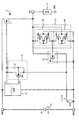
以下、図面を参照して本発明の実施の形態について説明する。図1に実施の形態1にかかる負荷駆動装置1の回路図を示す。図1に示すように、負荷駆動装置1は、電源10、負荷11、ドライバ回路12、制御回路13、補償回路14、出力トランジスタT1、電源端子PWR、接地端子GND1、接地端子GND2、出力端子OUTを有する。以下の説明では、電源端子PWRには、電源ラインが接続され、接地端子GND1には第1の接地ラインが接続され、接地端子GND2には第2の接地ラインが接続されるものとする。ドライバ回路12、制御回路13、補償回路14、出力トランジスタT1、電源端子PWR、接地端子GND2、及び出力端子OUTは、1つの半導体装置に設けられていてもよく、また、複数の半導体装置を利用するプリント回路基板等によって設けられていてもよい。
図3に実施の形態2にかかる負荷駆動装置2の回路図を示す。図3に示すように、負荷駆動装置2は、電源10、負荷11、ドライバ回路12、制御回路13、バックゲート制御回路15、補償回路16、出力トランジスタT1、抵抗R10、電源端子PWR、接地端子GND1、接地端子GND2、出力端子OUTを有する。ドライバ回路12、制御回路13、バックゲート制御回路15、補償回路16、出力トランジスタT1、抵抗R10、電源端子PWR、接地端子GND2、及び出力端子OUTは、1つの半導体装置に設けられていてもよく、また、複数の半導体装置を利用するプリント回路基板等によって設けられていてもよい。なお、以下の説明では、実施の形態1と同様のものについては実施の形態1と同様の符号を付して説明を省略する。
上記負荷駆動装置1、2では、接地端子GND2の電圧の上昇による出力トランジスタT1のオフ状態に関する不具合を解決できる。しかしながら、電源10が逆接続された場合における負荷駆動装置の保護を実現することはできない。そこで、実施の形態3では、接地端子GND2の電圧の上昇による出力トランジスタT1のオフ状態に関する不具合を解決に加え、電源10の逆接続時の保護も実現する。
実施の形態4にかかる負荷駆動装置4の回路図を図7に示す。図7に示すように、負荷駆動装置4は、実施の形態3における逆接続保護回路17の変形例を示す逆接続保護回路17aを有する。なお、逆接続保護回路17aを有する制御回路を図7では、制御回路13bとした。負荷駆動装置4において負荷駆動装置3と同様のものについては、負荷駆動装置3と同じ符号を付して説明を省略する。
実施の形態5にかかる負荷駆動装置5の回路図を図8に示す。図8に示すように、負荷駆動装置5は、負荷駆動装置3の補償回路14に替えて実施の形態3で示した補償回路16を用いる。負荷駆動装置5において負荷駆動装置3と同様のものについては、負荷駆動装置3と同じ符号を付して説明を省略する。
10 電源
11 負荷
12 ドライバ回路
13、13a、13b 制御回路
14、16 補償回路
15、18 バックゲート制御回路
15a、15b、18a、18b スイッチ回路
17、17a 逆接続保護回路
T1 出力トランジスタ
MN1 放電トランジスタ
MN2、MN7 補償トランジスタ
MN8 逆接続保護トランジスタ
MN3〜MN6、MN9〜MN12 NMOSトランジスタ
MN13 デプレッション型NMOSトランジスタ
R10、R11 抵抗
D10 クランプダイオード
PWR 電源端子
GND1、GND2 接地端子
Claims (6)
- 電源ラインと出力端子との間に接続された出力トランジスタと、
前記出力端子と第1の接地ラインとの間に接続される負荷と、
前記出力トランジスタのゲートと第2の接地ラインとの間に接続され、前記出力トランジスタのオン/オフを制御する制御回路と、
前記第2の接地ラインの電位が所定値以上となったときに導通し、前記出力トランジスタのオフ状態を維持する補償トランジスタと、
を有し、
前記制御回路は、
前記出力トランジスタのゲートと前記出力端子との間に接続される放電トランジスタと、
ダイオード接続されたトランジスタであって、前記出力トランジスタのゲートにカソード側端子が接続され、前記第2の接地ラインにアノード側端子が接続される逆接続保護トランジスタと、
前記第2の接地ラインに一端が接続される抵抗と、
前記抵抗の他端にカソードが接続され、前記電源ラインにアノードが接続される保護ダイオードと、
前記抵抗の他端と前記出力端子との間に接続され、前記抵抗の他端の電圧と前記出力端子の電圧との差に基づき前記逆接続保護トランジスタのバックゲートに与えるバックゲート電圧を制御するバックゲート制御回路と、を含む負荷駆動装置。 - 前記補償トランジスタは、前記出力トランジスタがオフ状態である場合に導通状態となる請求項1に記載の負荷駆動装置。
- 前記第1、第2の接地ラインは、同一の電源から電圧が供給され、それぞれ離れた位置に配置される請求項1又は2に記載の負荷駆動装置。
- 前記制御回路は、前記出力トランジスタのゲートと前記第2の接地ラインとの間に、前記逆接続保護トランジスタと直列接続されたデプレッション型トランジスタを有し、
前記デプレッション型トランジスタは、ゲートが前記逆接続保護トランジスタのゲートと共通接続され、バックゲートが前記逆接続保護トランジスタのバックゲートと共通接される請求項1乃至3のいずれか1項に記載の負荷駆動装置。 - 前記補償トランジスタは、ソース又はドレインの一方が前記出力端子と接続され、ソース又はドレインの他方が前記第2の接地ラインと接続され、ゲートが前記抵抗の他端に接続され、バックゲートに前記バックゲート制御回路から出力される前記バックゲート電圧が供給される請求項1乃至4のいずれか1項に記載の負荷駆動装置。
- 前記補償トランジスタは、前記出力トランジスタのゲートと前記出力端子との間に接続され、ゲートが前記抵抗を介して前記第2の接地ラインに接続される請求項1乃至4のいずれか1項に記載の負荷駆動装置。
Priority Applications (1)
| Application Number | Priority Date | Filing Date | Title |
|---|---|---|---|
| JP2008312946A JP5266029B2 (ja) | 2007-12-14 | 2008-12-09 | 負荷駆動装置 |
Applications Claiming Priority (3)
| Application Number | Priority Date | Filing Date | Title |
|---|---|---|---|
| JP2007322949 | 2007-12-14 | ||
| JP2007322949 | 2007-12-14 | ||
| JP2008312946A JP5266029B2 (ja) | 2007-12-14 | 2008-12-09 | 負荷駆動装置 |
Related Child Applications (1)
| Application Number | Title | Priority Date | Filing Date |
|---|---|---|---|
| JP2013071837A Division JP5519052B2 (ja) | 2007-12-14 | 2013-03-29 | 負荷駆動装置 |
Publications (3)
| Publication Number | Publication Date |
|---|---|
| JP2009165113A JP2009165113A (ja) | 2009-07-23 |
| JP2009165113A5 JP2009165113A5 (ja) | 2012-02-02 |
| JP5266029B2 true JP5266029B2 (ja) | 2013-08-21 |
Family
ID=40427532
Family Applications (2)
| Application Number | Title | Priority Date | Filing Date |
|---|---|---|---|
| JP2008312946A Expired - Fee Related JP5266029B2 (ja) | 2007-12-14 | 2008-12-09 | 負荷駆動装置 |
| JP2013071837A Expired - Fee Related JP5519052B2 (ja) | 2007-12-14 | 2013-03-29 | 負荷駆動装置 |
Family Applications After (1)
| Application Number | Title | Priority Date | Filing Date |
|---|---|---|---|
| JP2013071837A Expired - Fee Related JP5519052B2 (ja) | 2007-12-14 | 2013-03-29 | 負荷駆動装置 |
Country Status (3)
| Country | Link |
|---|---|
| US (2) | US8054106B2 (ja) |
| EP (1) | EP2071726B1 (ja) |
| JP (2) | JP5266029B2 (ja) |
Families Citing this family (16)
| Publication number | Priority date | Publication date | Assignee | Title |
|---|---|---|---|---|
| EP2071723B1 (en) * | 2007-12-12 | 2015-02-11 | Renesas Electronics Corporation | Load driving device |
| US8994708B2 (en) * | 2009-06-02 | 2015-03-31 | Sitronix Technology Corp. | Driver circuit for dot inversion of liquid crystals |
| JP5438468B2 (ja) | 2009-11-05 | 2014-03-12 | ルネサスエレクトロニクス株式会社 | 負荷駆動装置 |
| JP5438470B2 (ja) | 2009-11-05 | 2014-03-12 | ルネサスエレクトロニクス株式会社 | 電力供給制御回路 |
| JP5438469B2 (ja) * | 2009-11-05 | 2014-03-12 | ルネサスエレクトロニクス株式会社 | 負荷駆動装置 |
| JP5571596B2 (ja) * | 2010-07-02 | 2014-08-13 | ルネサスエレクトロニクス株式会社 | スイッチ回路装置 |
| US9024317B2 (en) * | 2010-12-24 | 2015-05-05 | Semiconductor Energy Laboratory Co., Ltd. | Semiconductor circuit, method for driving the same, storage device, register circuit, display device, and electronic device |
| US8884682B2 (en) | 2011-04-04 | 2014-11-11 | Renesas Electronics Corporation | Power semiconductor device |
| US8514530B2 (en) * | 2011-04-28 | 2013-08-20 | Freescale Semiconductor, Inc. | Load control and protection system |
| JP5842720B2 (ja) * | 2012-04-19 | 2016-01-13 | 株式会社ソシオネクスト | 出力回路 |
| JP6421624B2 (ja) * | 2015-01-29 | 2018-11-14 | 株式会社ソシオネクスト | 降圧電源回路および集積回路 |
| JP6753697B2 (ja) * | 2016-05-23 | 2020-09-09 | ローム株式会社 | Cmos出力回路 |
| CN107039422A (zh) * | 2016-12-06 | 2017-08-11 | 湘潭大学 | 一种集成电路esd全芯片防护电路 |
| CN109327211B (zh) * | 2017-07-31 | 2023-12-12 | 恩智浦有限公司 | 负载开关及其开关方法 |
| DE102018211872B4 (de) | 2018-07-17 | 2020-02-06 | HELLA GmbH & Co. KGaA | Schaltungsvorrichtung sowie Verfahren zum Betrieb einer Schaltungsvorrichtung |
| CN117016965B (zh) * | 2023-07-05 | 2024-04-05 | 湖南步升取暖科技股份有限公司 | 一种故障应急安全防护取暖茶几 |
Family Cites Families (16)
| Publication number | Priority date | Publication date | Assignee | Title |
|---|---|---|---|---|
| US4691129A (en) * | 1986-03-19 | 1987-09-01 | Siemens Aktiengesellschaft | Drive circuit for a power MOSFET with source-side load |
| DE3827730C1 (ja) * | 1988-08-16 | 1989-12-28 | Hella Kg Hueck & Co, 4780 Lippstadt, De | |
| US4931748A (en) * | 1988-08-26 | 1990-06-05 | Motorola, Inc. | Integrated circuit with clock generator |
| JP2504586B2 (ja) * | 1989-10-31 | 1996-06-05 | 東芝マイクロエレクトロニクス株式会社 | 接地外れ保護回路を有する電子回路装置 |
| JPH03166816A (ja) * | 1989-11-27 | 1991-07-18 | Hitachi Ltd | 半導体集積回路装置 |
| JP3123261B2 (ja) * | 1992-10-12 | 2001-01-09 | 株式会社デンソー | グロープラグ制御装置 |
| JP3386602B2 (ja) * | 1994-11-30 | 2003-03-17 | 株式会社東芝 | 出力回路装置 |
| US5592117A (en) * | 1995-04-11 | 1997-01-07 | International Rectifier Corporation | Integrated MOSgated power semiconductor device with high negative clamp voltage and fail safe operation |
| US6079113A (en) * | 1998-03-18 | 2000-06-27 | Helmrichs; Terry L. | Electronic radius gauge |
| US6236259B1 (en) * | 1999-10-04 | 2001-05-22 | Fairchild Semiconductor Corporation | Active undershoot hardened fet switch |
| US6647997B2 (en) * | 2001-05-16 | 2003-11-18 | Merrill K. Mohn | Paint gun washer |
| TW517422B (en) * | 2001-05-18 | 2003-01-11 | Palmax Technology Co Ltd | Input protection circuit of hand-held electrical apparatus |
| TWI253163B (en) * | 2003-06-27 | 2006-04-11 | Realtek Semiconductor Corp | Electrostatic discharge protection circuit |
| US8321173B2 (en) * | 2004-08-25 | 2012-11-27 | Wallance Daniel I | System and method for using magnetic sensors to track the position of an object |
| JP2007019812A (ja) * | 2005-07-07 | 2007-01-25 | Yazaki Corp | 電源の逆接続保護機能を備えた負荷駆動装置 |
| JP4895623B2 (ja) * | 2006-01-25 | 2012-03-14 | 株式会社オートネットワーク技術研究所 | 電力供給制御装置 |
-
2008
- 2008-12-09 JP JP2008312946A patent/JP5266029B2/ja not_active Expired - Fee Related
- 2008-12-10 EP EP08021471.1A patent/EP2071726B1/en not_active Expired - Fee Related
- 2008-12-11 US US12/314,491 patent/US8054106B2/en not_active Expired - Fee Related
-
2011
- 2011-10-07 US US13/317,028 patent/US8446185B2/en not_active Expired - Fee Related
-
2013
- 2013-03-29 JP JP2013071837A patent/JP5519052B2/ja not_active Expired - Fee Related
Also Published As
| Publication number | Publication date |
|---|---|
| US20120032707A1 (en) | 2012-02-09 |
| EP2071726B1 (en) | 2015-09-23 |
| JP2009165113A (ja) | 2009-07-23 |
| US8054106B2 (en) | 2011-11-08 |
| JP2013141310A (ja) | 2013-07-18 |
| EP2071726A2 (en) | 2009-06-17 |
| EP2071726A3 (en) | 2011-03-16 |
| US20090153225A1 (en) | 2009-06-18 |
| US8446185B2 (en) | 2013-05-21 |
| JP5519052B2 (ja) | 2014-06-11 |
Similar Documents
| Publication | Publication Date | Title |
|---|---|---|
| JP5266029B2 (ja) | 負荷駆動装置 | |
| US8116051B2 (en) | Power supply control circuit | |
| JP4597044B2 (ja) | 逆流防止回路 | |
| KR100702933B1 (ko) | 전원 클램프 회로 및 반도체 장치 | |
| JP5438470B2 (ja) | 電力供給制御回路 | |
| JP5438469B2 (ja) | 負荷駆動装置 | |
| JP5220240B2 (ja) | カップリング回路、このカップリング回路を含むドライバ回路、およびこのカップリング回路の制御方法 | |
| JPH08274618A (ja) | 耐過電圧集積回路出力バッファ | |
| JP5266030B2 (ja) | 負荷駆動装置 | |
| US6650520B2 (en) | Power supply reverse bias protection circuit for protecting both analog and digital devices coupled thereto | |
| JP6277151B2 (ja) | センサ装置 | |
| JP5438468B2 (ja) | 負荷駆動装置 | |
| JP5226474B2 (ja) | 半導体出力回路 | |
| US20190305544A1 (en) | Electric motor ground protection | |
| JP5435483B2 (ja) | 電源供給装置 | |
| US10659039B2 (en) | Semiconductor device | |
| CN117459041A (zh) | 高电压故障保护电路 | |
| JP2007110237A (ja) | インターフェース回路 |
Legal Events
| Date | Code | Title | Description |
|---|---|---|---|
| A521 | Request for written amendment filed |
Free format text: JAPANESE INTERMEDIATE CODE: A523 Effective date: 20111208 |
|
| A621 | Written request for application examination |
Free format text: JAPANESE INTERMEDIATE CODE: A621 Effective date: 20111208 |
|
| A977 | Report on retrieval |
Free format text: JAPANESE INTERMEDIATE CODE: A971007 Effective date: 20130218 |
|
| A131 | Notification of reasons for refusal |
Free format text: JAPANESE INTERMEDIATE CODE: A131 Effective date: 20130226 |
|
| A521 | Request for written amendment filed |
Free format text: JAPANESE INTERMEDIATE CODE: A523 Effective date: 20130329 |
|
| TRDD | Decision of grant or rejection written | ||
| A01 | Written decision to grant a patent or to grant a registration (utility model) |
Free format text: JAPANESE INTERMEDIATE CODE: A01 Effective date: 20130416 |
|
| A61 | First payment of annual fees (during grant procedure) |
Free format text: JAPANESE INTERMEDIATE CODE: A61 Effective date: 20130502 |
|
| R150 | Certificate of patent or registration of utility model |
Free format text: JAPANESE INTERMEDIATE CODE: R150 Ref document number: 5266029 Country of ref document: JP Free format text: JAPANESE INTERMEDIATE CODE: R150 |
|
| S531 | Written request for registration of change of domicile |
Free format text: JAPANESE INTERMEDIATE CODE: R313531 |
|
| R350 | Written notification of registration of transfer |
Free format text: JAPANESE INTERMEDIATE CODE: R350 |
|
| LAPS | Cancellation because of no payment of annual fees |