JP5215244B2 - 半導体装置 - Google Patents
半導体装置 Download PDFInfo
- Publication number
- JP5215244B2 JP5215244B2 JP2009145430A JP2009145430A JP5215244B2 JP 5215244 B2 JP5215244 B2 JP 5215244B2 JP 2009145430 A JP2009145430 A JP 2009145430A JP 2009145430 A JP2009145430 A JP 2009145430A JP 5215244 B2 JP5215244 B2 JP 5215244B2
- Authority
- JP
- Japan
- Prior art keywords
- semiconductor chip
- semiconductor chips
- semiconductor
- conductive
- stacked body
- Prior art date
- Legal status (The legal status is an assumption and is not a legal conclusion. Google has not performed a legal analysis and makes no representation as to the accuracy of the status listed.)
- Expired - Fee Related
Links
Images


Classifications
-
- H—ELECTRICITY
- H01—ELECTRIC ELEMENTS
- H01L—SEMICONDUCTOR DEVICES NOT COVERED BY CLASS H10
- H01L23/00—Details of semiconductor or other solid state devices
- H01L23/48—Arrangements for conducting electric current to or from the solid state body in operation, e.g. leads, terminal arrangements ; Selection of materials therefor
- H01L23/488—Arrangements for conducting electric current to or from the solid state body in operation, e.g. leads, terminal arrangements ; Selection of materials therefor consisting of soldered or bonded constructions
- H01L23/498—Leads, i.e. metallisations or lead-frames on insulating substrates, e.g. chip carriers
- H01L23/49811—Additional leads joined to the metallisation on the insulating substrate, e.g. pins, bumps, wires, flat leads
-
- H—ELECTRICITY
- H01—ELECTRIC ELEMENTS
- H01L—SEMICONDUCTOR DEVICES NOT COVERED BY CLASS H10
- H01L23/00—Details of semiconductor or other solid state devices
- H01L23/28—Encapsulations, e.g. encapsulating layers, coatings, e.g. for protection
- H01L23/31—Encapsulations, e.g. encapsulating layers, coatings, e.g. for protection characterised by the arrangement or shape
- H01L23/3107—Encapsulations, e.g. encapsulating layers, coatings, e.g. for protection characterised by the arrangement or shape the device being completely enclosed
- H01L23/3121—Encapsulations, e.g. encapsulating layers, coatings, e.g. for protection characterised by the arrangement or shape the device being completely enclosed a substrate forming part of the encapsulation
-
- H—ELECTRICITY
- H01—ELECTRIC ELEMENTS
- H01L—SEMICONDUCTOR DEVICES NOT COVERED BY CLASS H10
- H01L24/00—Arrangements for connecting or disconnecting semiconductor or solid-state bodies; Methods or apparatus related thereto
- H01L24/01—Means for bonding being attached to, or being formed on, the surface to be connected, e.g. chip-to-package, die-attach, "first-level" interconnects; Manufacturing methods related thereto
- H01L24/18—High density interconnect [HDI] connectors; Manufacturing methods related thereto
- H01L24/23—Structure, shape, material or disposition of the high density interconnect connectors after the connecting process
- H01L24/24—Structure, shape, material or disposition of the high density interconnect connectors after the connecting process of an individual high density interconnect connector
-
- H—ELECTRICITY
- H01—ELECTRIC ELEMENTS
- H01L—SEMICONDUCTOR DEVICES NOT COVERED BY CLASS H10
- H01L24/00—Arrangements for connecting or disconnecting semiconductor or solid-state bodies; Methods or apparatus related thereto
- H01L24/80—Methods for connecting semiconductor or other solid state bodies using means for bonding being attached to, or being formed on, the surface to be connected
- H01L24/82—Methods for connecting semiconductor or other solid state bodies using means for bonding being attached to, or being formed on, the surface to be connected by forming build-up interconnects at chip-level, e.g. for high density interconnects [HDI]
-
- H—ELECTRICITY
- H01—ELECTRIC ELEMENTS
- H01L—SEMICONDUCTOR DEVICES NOT COVERED BY CLASS H10
- H01L24/00—Arrangements for connecting or disconnecting semiconductor or solid-state bodies; Methods or apparatus related thereto
- H01L24/91—Methods for connecting semiconductor or solid state bodies including different methods provided for in two or more of groups H01L24/80 - H01L24/90
-
- H—ELECTRICITY
- H01—ELECTRIC ELEMENTS
- H01L—SEMICONDUCTOR DEVICES NOT COVERED BY CLASS H10
- H01L25/00—Assemblies consisting of a plurality of individual semiconductor or other solid state devices ; Multistep manufacturing processes thereof
- H01L25/03—Assemblies consisting of a plurality of individual semiconductor or other solid state devices ; Multistep manufacturing processes thereof all the devices being of a type provided for in the same subgroup of groups H01L27/00 - H01L33/00, or in a single subclass of H10K, H10N, e.g. assemblies of rectifier diodes
- H01L25/04—Assemblies consisting of a plurality of individual semiconductor or other solid state devices ; Multistep manufacturing processes thereof all the devices being of a type provided for in the same subgroup of groups H01L27/00 - H01L33/00, or in a single subclass of H10K, H10N, e.g. assemblies of rectifier diodes the devices not having separate containers
- H01L25/065—Assemblies consisting of a plurality of individual semiconductor or other solid state devices ; Multistep manufacturing processes thereof all the devices being of a type provided for in the same subgroup of groups H01L27/00 - H01L33/00, or in a single subclass of H10K, H10N, e.g. assemblies of rectifier diodes the devices not having separate containers the devices being of a type provided for in group H01L27/00
- H01L25/0657—Stacked arrangements of devices
-
- H—ELECTRICITY
- H01—ELECTRIC ELEMENTS
- H01L—SEMICONDUCTOR DEVICES NOT COVERED BY CLASS H10
- H01L2224/00—Indexing scheme for arrangements for connecting or disconnecting semiconductor or solid-state bodies and methods related thereto as covered by H01L24/00
- H01L2224/01—Means for bonding being attached to, or being formed on, the surface to be connected, e.g. chip-to-package, die-attach, "first-level" interconnects; Manufacturing methods related thereto
- H01L2224/18—High density interconnect [HDI] connectors; Manufacturing methods related thereto
- H01L2224/23—Structure, shape, material or disposition of the high density interconnect connectors after the connecting process
- H01L2224/24—Structure, shape, material or disposition of the high density interconnect connectors after the connecting process of an individual high density interconnect connector
- H01L2224/241—Disposition
- H01L2224/24135—Connecting between different semiconductor or solid-state bodies, i.e. chip-to-chip
- H01L2224/24145—Connecting between different semiconductor or solid-state bodies, i.e. chip-to-chip the bodies being stacked
-
- H—ELECTRICITY
- H01—ELECTRIC ELEMENTS
- H01L—SEMICONDUCTOR DEVICES NOT COVERED BY CLASS H10
- H01L2224/00—Indexing scheme for arrangements for connecting or disconnecting semiconductor or solid-state bodies and methods related thereto as covered by H01L24/00
- H01L2224/01—Means for bonding being attached to, or being formed on, the surface to be connected, e.g. chip-to-package, die-attach, "first-level" interconnects; Manufacturing methods related thereto
- H01L2224/26—Layer connectors, e.g. plate connectors, solder or adhesive layers; Manufacturing methods related thereto
- H01L2224/31—Structure, shape, material or disposition of the layer connectors after the connecting process
- H01L2224/32—Structure, shape, material or disposition of the layer connectors after the connecting process of an individual layer connector
- H01L2224/321—Disposition
- H01L2224/32135—Disposition the layer connector connecting between different semiconductor or solid-state bodies, i.e. chip-to-chip
- H01L2224/32145—Disposition the layer connector connecting between different semiconductor or solid-state bodies, i.e. chip-to-chip the bodies being stacked
-
- H—ELECTRICITY
- H01—ELECTRIC ELEMENTS
- H01L—SEMICONDUCTOR DEVICES NOT COVERED BY CLASS H10
- H01L2224/00—Indexing scheme for arrangements for connecting or disconnecting semiconductor or solid-state bodies and methods related thereto as covered by H01L24/00
- H01L2224/01—Means for bonding being attached to, or being formed on, the surface to be connected, e.g. chip-to-package, die-attach, "first-level" interconnects; Manufacturing methods related thereto
- H01L2224/42—Wire connectors; Manufacturing methods related thereto
- H01L2224/44—Structure, shape, material or disposition of the wire connectors prior to the connecting process
- H01L2224/45—Structure, shape, material or disposition of the wire connectors prior to the connecting process of an individual wire connector
- H01L2224/45001—Core members of the connector
- H01L2224/4501—Shape
- H01L2224/45012—Cross-sectional shape
- H01L2224/45015—Cross-sectional shape being circular
-
- H—ELECTRICITY
- H01—ELECTRIC ELEMENTS
- H01L—SEMICONDUCTOR DEVICES NOT COVERED BY CLASS H10
- H01L2224/00—Indexing scheme for arrangements for connecting or disconnecting semiconductor or solid-state bodies and methods related thereto as covered by H01L24/00
- H01L2224/01—Means for bonding being attached to, or being formed on, the surface to be connected, e.g. chip-to-package, die-attach, "first-level" interconnects; Manufacturing methods related thereto
- H01L2224/42—Wire connectors; Manufacturing methods related thereto
- H01L2224/44—Structure, shape, material or disposition of the wire connectors prior to the connecting process
- H01L2224/45—Structure, shape, material or disposition of the wire connectors prior to the connecting process of an individual wire connector
- H01L2224/45001—Core members of the connector
- H01L2224/45099—Material
- H01L2224/451—Material with a principal constituent of the material being a metal or a metalloid, e.g. boron (B), silicon (Si), germanium (Ge), arsenic (As), antimony (Sb), tellurium (Te) and polonium (Po), and alloys thereof
- H01L2224/45117—Material with a principal constituent of the material being a metal or a metalloid, e.g. boron (B), silicon (Si), germanium (Ge), arsenic (As), antimony (Sb), tellurium (Te) and polonium (Po), and alloys thereof the principal constituent melting at a temperature of greater than or equal to 400°C and less than 950°C
- H01L2224/45124—Aluminium (Al) as principal constituent
-
- H—ELECTRICITY
- H01—ELECTRIC ELEMENTS
- H01L—SEMICONDUCTOR DEVICES NOT COVERED BY CLASS H10
- H01L2224/00—Indexing scheme for arrangements for connecting or disconnecting semiconductor or solid-state bodies and methods related thereto as covered by H01L24/00
- H01L2224/01—Means for bonding being attached to, or being formed on, the surface to be connected, e.g. chip-to-package, die-attach, "first-level" interconnects; Manufacturing methods related thereto
- H01L2224/42—Wire connectors; Manufacturing methods related thereto
- H01L2224/44—Structure, shape, material or disposition of the wire connectors prior to the connecting process
- H01L2224/45—Structure, shape, material or disposition of the wire connectors prior to the connecting process of an individual wire connector
- H01L2224/45001—Core members of the connector
- H01L2224/45099—Material
- H01L2224/451—Material with a principal constituent of the material being a metal or a metalloid, e.g. boron (B), silicon (Si), germanium (Ge), arsenic (As), antimony (Sb), tellurium (Te) and polonium (Po), and alloys thereof
- H01L2224/45138—Material with a principal constituent of the material being a metal or a metalloid, e.g. boron (B), silicon (Si), germanium (Ge), arsenic (As), antimony (Sb), tellurium (Te) and polonium (Po), and alloys thereof the principal constituent melting at a temperature of greater than or equal to 950°C and less than 1550°C
- H01L2224/45144—Gold (Au) as principal constituent
-
- H—ELECTRICITY
- H01—ELECTRIC ELEMENTS
- H01L—SEMICONDUCTOR DEVICES NOT COVERED BY CLASS H10
- H01L2224/00—Indexing scheme for arrangements for connecting or disconnecting semiconductor or solid-state bodies and methods related thereto as covered by H01L24/00
- H01L2224/01—Means for bonding being attached to, or being formed on, the surface to be connected, e.g. chip-to-package, die-attach, "first-level" interconnects; Manufacturing methods related thereto
- H01L2224/42—Wire connectors; Manufacturing methods related thereto
- H01L2224/44—Structure, shape, material or disposition of the wire connectors prior to the connecting process
- H01L2224/45—Structure, shape, material or disposition of the wire connectors prior to the connecting process of an individual wire connector
- H01L2224/45001—Core members of the connector
- H01L2224/45099—Material
- H01L2224/451—Material with a principal constituent of the material being a metal or a metalloid, e.g. boron (B), silicon (Si), germanium (Ge), arsenic (As), antimony (Sb), tellurium (Te) and polonium (Po), and alloys thereof
- H01L2224/45138—Material with a principal constituent of the material being a metal or a metalloid, e.g. boron (B), silicon (Si), germanium (Ge), arsenic (As), antimony (Sb), tellurium (Te) and polonium (Po), and alloys thereof the principal constituent melting at a temperature of greater than or equal to 950°C and less than 1550°C
- H01L2224/45147—Copper (Cu) as principal constituent
-
- H—ELECTRICITY
- H01—ELECTRIC ELEMENTS
- H01L—SEMICONDUCTOR DEVICES NOT COVERED BY CLASS H10
- H01L2224/00—Indexing scheme for arrangements for connecting or disconnecting semiconductor or solid-state bodies and methods related thereto as covered by H01L24/00
- H01L2224/01—Means for bonding being attached to, or being formed on, the surface to be connected, e.g. chip-to-package, die-attach, "first-level" interconnects; Manufacturing methods related thereto
- H01L2224/42—Wire connectors; Manufacturing methods related thereto
- H01L2224/44—Structure, shape, material or disposition of the wire connectors prior to the connecting process
- H01L2224/45—Structure, shape, material or disposition of the wire connectors prior to the connecting process of an individual wire connector
- H01L2224/45001—Core members of the connector
- H01L2224/45099—Material
- H01L2224/451—Material with a principal constituent of the material being a metal or a metalloid, e.g. boron (B), silicon (Si), germanium (Ge), arsenic (As), antimony (Sb), tellurium (Te) and polonium (Po), and alloys thereof
- H01L2224/45163—Material with a principal constituent of the material being a metal or a metalloid, e.g. boron (B), silicon (Si), germanium (Ge), arsenic (As), antimony (Sb), tellurium (Te) and polonium (Po), and alloys thereof the principal constituent melting at a temperature of greater than 1550°C
- H01L2224/45184—Tungsten (W) as principal constituent
-
- H—ELECTRICITY
- H01—ELECTRIC ELEMENTS
- H01L—SEMICONDUCTOR DEVICES NOT COVERED BY CLASS H10
- H01L2224/00—Indexing scheme for arrangements for connecting or disconnecting semiconductor or solid-state bodies and methods related thereto as covered by H01L24/00
- H01L2224/01—Means for bonding being attached to, or being formed on, the surface to be connected, e.g. chip-to-package, die-attach, "first-level" interconnects; Manufacturing methods related thereto
- H01L2224/42—Wire connectors; Manufacturing methods related thereto
- H01L2224/44—Structure, shape, material or disposition of the wire connectors prior to the connecting process
- H01L2224/45—Structure, shape, material or disposition of the wire connectors prior to the connecting process of an individual wire connector
- H01L2224/4554—Coating
- H01L2224/45599—Material
- H01L2224/456—Material with a principal constituent of the material being a metal or a metalloid, e.g. boron (B), silicon (Si), germanium (Ge), arsenic (As), antimony (Sb), tellurium (Te) and polonium (Po), and alloys thereof
- H01L2224/45663—Material with a principal constituent of the material being a metal or a metalloid, e.g. boron (B), silicon (Si), germanium (Ge), arsenic (As), antimony (Sb), tellurium (Te) and polonium (Po), and alloys thereof the principal constituent melting at a temperature of greater than 1550°C
- H01L2224/45684—Tungsten (W) as principal constituent
-
- H—ELECTRICITY
- H01—ELECTRIC ELEMENTS
- H01L—SEMICONDUCTOR DEVICES NOT COVERED BY CLASS H10
- H01L2224/00—Indexing scheme for arrangements for connecting or disconnecting semiconductor or solid-state bodies and methods related thereto as covered by H01L24/00
- H01L2224/01—Means for bonding being attached to, or being formed on, the surface to be connected, e.g. chip-to-package, die-attach, "first-level" interconnects; Manufacturing methods related thereto
- H01L2224/42—Wire connectors; Manufacturing methods related thereto
- H01L2224/47—Structure, shape, material or disposition of the wire connectors after the connecting process
- H01L2224/48—Structure, shape, material or disposition of the wire connectors after the connecting process of an individual wire connector
- H01L2224/481—Disposition
- H01L2224/48135—Connecting between different semiconductor or solid-state bodies, i.e. chip-to-chip
- H01L2224/48137—Connecting between different semiconductor or solid-state bodies, i.e. chip-to-chip the bodies being arranged next to each other, e.g. on a common substrate
-
- H—ELECTRICITY
- H01—ELECTRIC ELEMENTS
- H01L—SEMICONDUCTOR DEVICES NOT COVERED BY CLASS H10
- H01L2225/00—Details relating to assemblies covered by the group H01L25/00 but not provided for in its subgroups
- H01L2225/03—All the devices being of a type provided for in the same subgroup of groups H01L27/00 - H01L33/648 and H10K99/00
- H01L2225/04—All the devices being of a type provided for in the same subgroup of groups H01L27/00 - H01L33/648 and H10K99/00 the devices not having separate containers
- H01L2225/065—All the devices being of a type provided for in the same subgroup of groups H01L27/00 - H01L33/648 and H10K99/00 the devices not having separate containers the devices being of a type provided for in group H01L27/00
- H01L2225/06503—Stacked arrangements of devices
- H01L2225/06517—Bump or bump-like direct electrical connections from device to substrate
-
- H—ELECTRICITY
- H01—ELECTRIC ELEMENTS
- H01L—SEMICONDUCTOR DEVICES NOT COVERED BY CLASS H10
- H01L2225/00—Details relating to assemblies covered by the group H01L25/00 but not provided for in its subgroups
- H01L2225/03—All the devices being of a type provided for in the same subgroup of groups H01L27/00 - H01L33/648 and H10K99/00
- H01L2225/04—All the devices being of a type provided for in the same subgroup of groups H01L27/00 - H01L33/648 and H10K99/00 the devices not having separate containers
- H01L2225/065—All the devices being of a type provided for in the same subgroup of groups H01L27/00 - H01L33/648 and H10K99/00 the devices not having separate containers the devices being of a type provided for in group H01L27/00
- H01L2225/06503—Stacked arrangements of devices
- H01L2225/06551—Conductive connections on the side of the device
-
- H—ELECTRICITY
- H01—ELECTRIC ELEMENTS
- H01L—SEMICONDUCTOR DEVICES NOT COVERED BY CLASS H10
- H01L24/00—Arrangements for connecting or disconnecting semiconductor or solid-state bodies; Methods or apparatus related thereto
- H01L24/01—Means for bonding being attached to, or being formed on, the surface to be connected, e.g. chip-to-package, die-attach, "first-level" interconnects; Manufacturing methods related thereto
- H01L24/42—Wire connectors; Manufacturing methods related thereto
- H01L24/44—Structure, shape, material or disposition of the wire connectors prior to the connecting process
- H01L24/45—Structure, shape, material or disposition of the wire connectors prior to the connecting process of an individual wire connector
-
- H—ELECTRICITY
- H01—ELECTRIC ELEMENTS
- H01L—SEMICONDUCTOR DEVICES NOT COVERED BY CLASS H10
- H01L25/00—Assemblies consisting of a plurality of individual semiconductor or other solid state devices ; Multistep manufacturing processes thereof
- H01L25/50—Multistep manufacturing processes of assemblies consisting of devices, each device being of a type provided for in group H01L27/00 or H01L29/00
-
- H—ELECTRICITY
- H01—ELECTRIC ELEMENTS
- H01L—SEMICONDUCTOR DEVICES NOT COVERED BY CLASS H10
- H01L2924/00—Indexing scheme for arrangements or methods for connecting or disconnecting semiconductor or solid-state bodies as covered by H01L24/00
- H01L2924/0001—Technical content checked by a classifier
- H01L2924/00014—Technical content checked by a classifier the subject-matter covered by the group, the symbol of which is combined with the symbol of this group, being disclosed without further technical details
-
- H—ELECTRICITY
- H01—ELECTRIC ELEMENTS
- H01L—SEMICONDUCTOR DEVICES NOT COVERED BY CLASS H10
- H01L2924/00—Indexing scheme for arrangements or methods for connecting or disconnecting semiconductor or solid-state bodies as covered by H01L24/00
- H01L2924/01—Chemical elements
- H01L2924/01005—Boron [B]
-
- H—ELECTRICITY
- H01—ELECTRIC ELEMENTS
- H01L—SEMICONDUCTOR DEVICES NOT COVERED BY CLASS H10
- H01L2924/00—Indexing scheme for arrangements or methods for connecting or disconnecting semiconductor or solid-state bodies as covered by H01L24/00
- H01L2924/01—Chemical elements
- H01L2924/01006—Carbon [C]
-
- H—ELECTRICITY
- H01—ELECTRIC ELEMENTS
- H01L—SEMICONDUCTOR DEVICES NOT COVERED BY CLASS H10
- H01L2924/00—Indexing scheme for arrangements or methods for connecting or disconnecting semiconductor or solid-state bodies as covered by H01L24/00
- H01L2924/01—Chemical elements
- H01L2924/01013—Aluminum [Al]
-
- H—ELECTRICITY
- H01—ELECTRIC ELEMENTS
- H01L—SEMICONDUCTOR DEVICES NOT COVERED BY CLASS H10
- H01L2924/00—Indexing scheme for arrangements or methods for connecting or disconnecting semiconductor or solid-state bodies as covered by H01L24/00
- H01L2924/01—Chemical elements
- H01L2924/01014—Silicon [Si]
-
- H—ELECTRICITY
- H01—ELECTRIC ELEMENTS
- H01L—SEMICONDUCTOR DEVICES NOT COVERED BY CLASS H10
- H01L2924/00—Indexing scheme for arrangements or methods for connecting or disconnecting semiconductor or solid-state bodies as covered by H01L24/00
- H01L2924/01—Chemical elements
- H01L2924/01029—Copper [Cu]
-
- H—ELECTRICITY
- H01—ELECTRIC ELEMENTS
- H01L—SEMICONDUCTOR DEVICES NOT COVERED BY CLASS H10
- H01L2924/00—Indexing scheme for arrangements or methods for connecting or disconnecting semiconductor or solid-state bodies as covered by H01L24/00
- H01L2924/01—Chemical elements
- H01L2924/01033—Arsenic [As]
-
- H—ELECTRICITY
- H01—ELECTRIC ELEMENTS
- H01L—SEMICONDUCTOR DEVICES NOT COVERED BY CLASS H10
- H01L2924/00—Indexing scheme for arrangements or methods for connecting or disconnecting semiconductor or solid-state bodies as covered by H01L24/00
- H01L2924/01—Chemical elements
- H01L2924/01047—Silver [Ag]
-
- H—ELECTRICITY
- H01—ELECTRIC ELEMENTS
- H01L—SEMICONDUCTOR DEVICES NOT COVERED BY CLASS H10
- H01L2924/00—Indexing scheme for arrangements or methods for connecting or disconnecting semiconductor or solid-state bodies as covered by H01L24/00
- H01L2924/01—Chemical elements
- H01L2924/0105—Tin [Sn]
-
- H—ELECTRICITY
- H01—ELECTRIC ELEMENTS
- H01L—SEMICONDUCTOR DEVICES NOT COVERED BY CLASS H10
- H01L2924/00—Indexing scheme for arrangements or methods for connecting or disconnecting semiconductor or solid-state bodies as covered by H01L24/00
- H01L2924/01—Chemical elements
- H01L2924/01074—Tungsten [W]
-
- H—ELECTRICITY
- H01—ELECTRIC ELEMENTS
- H01L—SEMICONDUCTOR DEVICES NOT COVERED BY CLASS H10
- H01L2924/00—Indexing scheme for arrangements or methods for connecting or disconnecting semiconductor or solid-state bodies as covered by H01L24/00
- H01L2924/01—Chemical elements
- H01L2924/01079—Gold [Au]
-
- H—ELECTRICITY
- H01—ELECTRIC ELEMENTS
- H01L—SEMICONDUCTOR DEVICES NOT COVERED BY CLASS H10
- H01L2924/00—Indexing scheme for arrangements or methods for connecting or disconnecting semiconductor or solid-state bodies as covered by H01L24/00
- H01L2924/01—Chemical elements
- H01L2924/01082—Lead [Pb]
-
- H—ELECTRICITY
- H01—ELECTRIC ELEMENTS
- H01L—SEMICONDUCTOR DEVICES NOT COVERED BY CLASS H10
- H01L2924/00—Indexing scheme for arrangements or methods for connecting or disconnecting semiconductor or solid-state bodies as covered by H01L24/00
- H01L2924/013—Alloys
- H01L2924/014—Solder alloys
-
- H—ELECTRICITY
- H01—ELECTRIC ELEMENTS
- H01L—SEMICONDUCTOR DEVICES NOT COVERED BY CLASS H10
- H01L2924/00—Indexing scheme for arrangements or methods for connecting or disconnecting semiconductor or solid-state bodies as covered by H01L24/00
- H01L2924/10—Details of semiconductor or other solid state devices to be connected
- H01L2924/11—Device type
- H01L2924/14—Integrated circuits
-
- H—ELECTRICITY
- H01—ELECTRIC ELEMENTS
- H01L—SEMICONDUCTOR DEVICES NOT COVERED BY CLASS H10
- H01L2924/00—Indexing scheme for arrangements or methods for connecting or disconnecting semiconductor or solid-state bodies as covered by H01L24/00
- H01L2924/15—Details of package parts other than the semiconductor or other solid state devices to be connected
- H01L2924/181—Encapsulation
- H01L2924/1815—Shape
-
- H—ELECTRICITY
- H01—ELECTRIC ELEMENTS
- H01L—SEMICONDUCTOR DEVICES NOT COVERED BY CLASS H10
- H01L2924/00—Indexing scheme for arrangements or methods for connecting or disconnecting semiconductor or solid-state bodies as covered by H01L24/00
- H01L2924/20—Parameters
- H01L2924/207—Diameter ranges
- H01L2924/20751—Diameter ranges larger or equal to 10 microns less than 20 microns
-
- H—ELECTRICITY
- H01—ELECTRIC ELEMENTS
- H01L—SEMICONDUCTOR DEVICES NOT COVERED BY CLASS H10
- H01L2924/00—Indexing scheme for arrangements or methods for connecting or disconnecting semiconductor or solid-state bodies as covered by H01L24/00
- H01L2924/20—Parameters
- H01L2924/207—Diameter ranges
- H01L2924/20752—Diameter ranges larger or equal to 20 microns less than 30 microns
-
- H—ELECTRICITY
- H01—ELECTRIC ELEMENTS
- H01L—SEMICONDUCTOR DEVICES NOT COVERED BY CLASS H10
- H01L2924/00—Indexing scheme for arrangements or methods for connecting or disconnecting semiconductor or solid-state bodies as covered by H01L24/00
- H01L2924/30—Technical effects
- H01L2924/301—Electrical effects
- H01L2924/30105—Capacitance
-
- H—ELECTRICITY
- H01—ELECTRIC ELEMENTS
- H01L—SEMICONDUCTOR DEVICES NOT COVERED BY CLASS H10
- H01L2924/00—Indexing scheme for arrangements or methods for connecting or disconnecting semiconductor or solid-state bodies as covered by H01L24/00
- H01L2924/30—Technical effects
- H01L2924/301—Electrical effects
- H01L2924/30107—Inductance
Landscapes
- Engineering & Computer Science (AREA)
- Microelectronics & Electronic Packaging (AREA)
- Power Engineering (AREA)
- Computer Hardware Design (AREA)
- Physics & Mathematics (AREA)
- Condensed Matter Physics & Semiconductors (AREA)
- General Physics & Mathematics (AREA)
- Wire Bonding (AREA)
Description
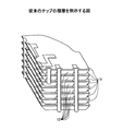
図2は、本発明の第1の実施の形態に係る半導体チップ積層体を例示する断面図である。図2を参照するに、半導体チップ積層体20Aは、配線基板51と、配線基板51上に載置されたチップ積層体52Cとを有する。チップ積層体52Cは、パッド33を含む複数の半導体チップ32と、それぞれのパッド33に接続されたボンディングワイヤ34aと、導電性部材47と、封止樹脂48とを有する。
例えば、外径が6インチ、8インチまたは12インチの半導体ウエハを準備し、バックグラインド等による薄型化を施し、さらに個々の半導体チップにダイシング(個片化)する。ダイシングを終えた半導体チップは、ダイシングテープ上に置かれている。
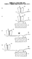
工程a.において、S100で準備した個々の半導体チップを、ダイシングテープからピックアップして、仮接着フィルム上に載置する。仮接着フィルムの材質としては、例えば、ポリエステルフィルムを使用することができる。
個々の半導体チップ32を前出の図5又は図7で示した仮接着フィルム31上から剥離し、ボンディングワイヤ34aを有する半導体チップ32の背面41bに絶縁樹脂42を塗布する。絶縁樹脂42の塗布は、周知のスクリーン印刷法、スピンコート法またはフィルム状シートの貼り付け等により行うことができる。
図8は、ボンディングワイヤ34a及び絶縁樹脂42を有する半導体チップ32が、配線基板51上に載置され、全体としてチップ積層体52Aが形成された状態を示している。個々の半導体チップをピックアップして、チップ積層を行うが、チップ積層体52Aの形成のためには、ダイマウント装置またはフリップチップマウンタ装置を使用し、半導体チップのアライメントと固定を行う。チップ積層体の配線基板への搭載における絶縁樹脂による固定は、例えば、150℃の温度で30分の温度条件により行う。
図9は、半導体チップ32の有するボンディングワイヤ34aの端部が、導電性部材47により配線基板51上の接続端子61と導電接続され、全体としてチップ積層体52Bが形成された状態を示している。前出の図8において積層された半導体チップ32の側面から突出する各ボンディングワイヤ34aの端部は、導電性部材47により配線基板51の接続端子61と導電接続されている。導電性部材47としては、例えば、高粘度でチクソ性を有する銀ペーストやはんだ等を使用することができる。
図9に示す積層体・基板接続工程の後に、チップ積層体、接続端子と接続された導電性連結材及び配線基板について、その全体または一部を封止樹脂48により封止することにより、図2に示す半導体チップ積層体20Aが完成する。
各々の半導体チップに接続されたボンディングワイヤを、導電性部材により配線基板の接続端子と導電接続する際に、各々の半導体チップの側面と導電性部材との間に所定の間隔を空けるようにする。その結果、各々の半導体チップの側面に絶縁膜を形成する工程が不要となり、半導体チップ積層体の形成工程を簡素化して、生産性の向上を図ることができる。
図10は、本発明の第2の実施の形態に係る半導体チップ積層体を例示する断面図である。同図中、図2と同一の構成部分については同一符号を付し、その説明を省略する場合がある。
第1の実施の形態と同様の効果を奏するが、更に以下の効果を奏する。すなわち、半導体チップ積層体に搭載できる半導体チップの種類を増やすことができる。
図11は、本発明の第3の実施の形態に係る半導体チップ積層体を例示する断面図である。同図中、図2と同一の構成部分については同一符号を付し、その説明を省略する場合がある。
第1の実施の形態と同様の効果を奏するが、更に以下の効果を奏する。すなわち、半導体チップ積層体において、ボンディングワイヤの長さを調整することにより、チップサイズが異なる半導体チップを積層することができる。
図12は、本発明の第4の実施の形態に係る半導体チップ積層体を例示する断面図である。同図中、図2と同一の構成部分については同一符号を付し、その説明を省略する場合がある。
第1の実施の形態と同様の効果を奏するが、更に以下の効果を奏する。すなわち、図4又は図6に示す工程と同一工程において、各々の半導体チップの集積回路面側に絶縁樹脂を塗布することができるため、半導体チップ積層体の形成工程を簡素化して、生産性の向上を図ることができる。
図13は、本発明の第5の実施の形態に係る半導体チップ積層体を例示する断面図である。同図中、図2と同一の構成部分については同一符号を付し、その説明を省略する場合がある。
第1の実施の形態と同様の効果を奏するが、更に以下の効果を奏する。すなわち、例えば、KGD(Known Good Die)としてのメモリとロジックの複合した半導体チップの積層体等を構成することができるので、半導体パッケージの設計において、半導体チップ積層体の形態を利用できる半導体チップの範囲を拡大することができる。そして、半導体チップの積層体をコンパクトな形態にすることができるので、さらに性能の向上を図ることができる。
以上、本発明の好ましい実施の形態について詳説したが、本発明は、上述した実施の形態に制限されることはなく、本発明の範囲を逸脱することなく、上述した実施の形態に種々の変形及び置換を加えることができる。
31 仮接着フィルム
32、32A、32B、32C、32D 半導体チップ
33 パッド
34、34a、34b、34c ボンディングワイヤ
35 間隙
36 導電性連結材
37 切断箇所
41a 集積回路面
41b 背面
42、46 絶縁樹脂
47 導電性部材
48 封止樹脂
49 シリンジ
51 配線基板
52A、52B、52C、52D、52E、52F、52G チップ積層体
61 接続端子
70 ボンディングツール
71 底面部
72、73 溝
74 孔部
81 パッド
82 バンプ
83 接続端子
84 絶縁樹脂
h1、h2 深さ
θ1,θ2 開口角度
W1 間隔
Claims (5)
- 接続端子を有する配線基板と、
前記配線基板上に積層された、パッドを有する複数の半導体チップと、
一方の端部が前記複数の半導体チップの前記パッドと接続され、他方の端部が前記複数の半導体チップの側面から突出する導電性連結材と、
前記複数の半導体チップにおける前記導電性連結材の前記他方の端部と前記配線基板の前記接続端子とを接続する導電性部材と、を有し、
前記複数の半導体チップの側面には前記複数の半導体チップの各々を構成する導電性材料が露出しており、前記複数の半導体チップの側面と前記導電性部材との間には間隙が設けられ、
前記導電性部材は、導電性ペースト、又は、はんだの何れか一の材料であり、
前記複数の半導体チップ、前記導電性連結材、前記導電性部材、及び前記間隙は、同一の封止樹脂により覆われている半導体チップ積層体。 - 前記配線基板上に積層された前記複数の半導体チップのうち、隣接する半導体チップにおいて、前記導電性連結材の前記他方の端部が異なる方向に突出している請求項1記載の半導体チップ積層体。
- 前記配線基板上に積層された前記複数の半導体チップのうち、少なくとも1つの半導体チップは、他の半導体チップと大きさが異なる請求項1又は2記載の半導体チップ積層体。
- 前記配線基板上に積層された前記複数の半導体チップのうち、前記配線基板に対向する半導体チップは、前記配線基板とフリップチップ接続されている請求項1乃至3の何れか一項記載の半導体チップ積層体。
- 前記導電性部材は、チクソ性を有する材料である請求項1乃至4の何れか一項記載の半導体チップ積層体。
Priority Applications (2)
| Application Number | Priority Date | Filing Date | Title |
|---|---|---|---|
| JP2009145430A JP5215244B2 (ja) | 2009-06-18 | 2009-06-18 | 半導体装置 |
| US12/768,938 US8058717B2 (en) | 2009-06-18 | 2010-04-28 | Laminated body of semiconductor chips including pads mutually connected to conductive member |
Applications Claiming Priority (1)
| Application Number | Priority Date | Filing Date | Title |
|---|---|---|---|
| JP2009145430A JP5215244B2 (ja) | 2009-06-18 | 2009-06-18 | 半導体装置 |
Publications (3)
| Publication Number | Publication Date |
|---|---|
| JP2011003715A JP2011003715A (ja) | 2011-01-06 |
| JP2011003715A5 JP2011003715A5 (ja) | 2012-06-07 |
| JP5215244B2 true JP5215244B2 (ja) | 2013-06-19 |
Family
ID=43353539
Family Applications (1)
| Application Number | Title | Priority Date | Filing Date |
|---|---|---|---|
| JP2009145430A Expired - Fee Related JP5215244B2 (ja) | 2009-06-18 | 2009-06-18 | 半導体装置 |
Country Status (2)
| Country | Link |
|---|---|
| US (1) | US8058717B2 (ja) |
| JP (1) | JP5215244B2 (ja) |
Families Citing this family (15)
| Publication number | Priority date | Publication date | Assignee | Title |
|---|---|---|---|---|
| US8680686B2 (en) * | 2010-06-29 | 2014-03-25 | Spansion Llc | Method and system for thin multi chip stack package with film on wire and copper wire |
| US9530753B2 (en) * | 2011-09-23 | 2016-12-27 | STATS ChipPAC Pte. Ltd. | Integrated circuit packaging system with chip stacking and method of manufacture thereof |
| US9093457B2 (en) | 2012-08-22 | 2015-07-28 | Freescale Semiconductor Inc. | Stacked microelectronic packages having patterned sidewall conductors and methods for the fabrication thereof |
| US9064977B2 (en) | 2012-08-22 | 2015-06-23 | Freescale Semiconductor Inc. | Stacked microelectronic packages having sidewall conductors and methods for the fabrication thereof |
| US9190390B2 (en) | 2012-08-22 | 2015-11-17 | Freescale Semiconductor Inc. | Stacked microelectronic packages having sidewall conductors and methods for the fabrication thereof |
| US8860202B2 (en) * | 2012-08-29 | 2014-10-14 | Macronix International Co., Ltd. | Chip stack structure and manufacturing method thereof |
| US9299670B2 (en) | 2013-03-14 | 2016-03-29 | Freescale Semiconductor, Inc. | Stacked microelectronic packages having sidewall conductors and methods for the fabrication thereof |
| US9524950B2 (en) | 2013-05-31 | 2016-12-20 | Freescale Semiconductor, Inc. | Stacked microelectronic packages having sidewall conductors and methods for the fabrication thereof |
| KR102099878B1 (ko) * | 2013-07-11 | 2020-04-10 | 삼성전자 주식회사 | 반도체 패키지 |
| US9036363B2 (en) | 2013-09-30 | 2015-05-19 | Freescale Semiconductor, Inc. | Devices and stacked microelectronic packages with parallel conductors and intra-conductor isolator structures and methods of their fabrication |
| US9025340B2 (en) | 2013-09-30 | 2015-05-05 | Freescale Semiconductor, Inc. | Devices and stacked microelectronic packages with in-trench package surface conductors and methods of their fabrication |
| US9305911B2 (en) | 2013-12-05 | 2016-04-05 | Freescale Semiconductor, Inc. | Devices and stacked microelectronic packages with package surface conductors and adjacent trenches and methods of their fabrication |
| US9263420B2 (en) | 2013-12-05 | 2016-02-16 | Freescale Semiconductor, Inc. | Devices and stacked microelectronic packages with package surface conductors and methods of their fabrication |
| US10388607B2 (en) | 2014-12-17 | 2019-08-20 | Nxp Usa, Inc. | Microelectronic devices with multi-layer package surface conductors and methods of their fabrication |
| WO2018182598A1 (en) * | 2017-03-29 | 2018-10-04 | Intel Corporation | Side mounted interconnect bridges |
Family Cites Families (23)
| Publication number | Priority date | Publication date | Assignee | Title |
|---|---|---|---|---|
| US5675180A (en) * | 1994-06-23 | 1997-10-07 | Cubic Memory, Inc. | Vertical interconnect process for silicon segments |
| JP3476383B2 (ja) * | 1999-05-27 | 2003-12-10 | シャープ株式会社 | 半導体積層パッケージ |
| JP3681155B2 (ja) * | 1999-12-22 | 2005-08-10 | 新光電気工業株式会社 | 電子部品の実装構造、電子部品装置、電子部品の実装方法及び電子部品装置の製造方法 |
| JP3708399B2 (ja) * | 2000-03-13 | 2005-10-19 | 株式会社東芝 | 半導体装置及びその製造方法 |
| JP4361670B2 (ja) * | 2000-08-02 | 2009-11-11 | 富士通マイクロエレクトロニクス株式会社 | 半導体素子積層体、半導体素子積層体の製造方法、及び半導体装置 |
| JP2002184937A (ja) * | 2000-12-18 | 2002-06-28 | Shinko Electric Ind Co Ltd | 半導体装置の実装構造 |
| US7215018B2 (en) * | 2004-04-13 | 2007-05-08 | Vertical Circuits, Inc. | Stacked die BGA or LGA component assembly |
| CN100539135C (zh) * | 2004-09-08 | 2009-09-09 | 松下电器产业株式会社 | 立体电路装置、使用它的电子机器及其制造方法 |
| JP4551321B2 (ja) * | 2005-07-21 | 2010-09-29 | 新光電気工業株式会社 | 電子部品実装構造及びその製造方法 |
| JP4566866B2 (ja) * | 2005-09-07 | 2010-10-20 | 新光電気工業株式会社 | 半導体パッケージ、半導体パッケージの実装構造、半導体パッケージの製造方法 |
| KR100794658B1 (ko) * | 2006-07-07 | 2008-01-14 | 삼성전자주식회사 | 반도체 칩 제조 방법, 이에 의해 형성된 반도체 칩 및 이를포함하는 칩 스택 패키지 |
| KR100813625B1 (ko) * | 2006-11-15 | 2008-03-14 | 삼성전자주식회사 | 반도체 소자 패키지 |
| SG146460A1 (en) * | 2007-03-12 | 2008-10-30 | Micron Technology Inc | Apparatus for packaging semiconductor devices, packaged semiconductor components, methods of manufacturing apparatus for packaging semiconductor devices, and methods of manufacturing semiconductor components |
| KR100914977B1 (ko) * | 2007-06-18 | 2009-09-02 | 주식회사 하이닉스반도체 | 스택 패키지의 제조 방법 |
| JP5110995B2 (ja) * | 2007-07-20 | 2012-12-26 | 新光電気工業株式会社 | 積層型半導体装置及びその製造方法 |
| JP5110996B2 (ja) * | 2007-07-20 | 2012-12-26 | 新光電気工業株式会社 | 積層型半導体装置の製造方法 |
| JP5049684B2 (ja) * | 2007-07-20 | 2012-10-17 | 新光電気工業株式会社 | 積層型半導体装置及びその製造方法 |
| US7781877B2 (en) * | 2007-08-07 | 2010-08-24 | Micron Technology, Inc. | Packaged integrated circuit devices with through-body conductive vias, and methods of making same |
| JP2009071095A (ja) * | 2007-09-14 | 2009-04-02 | Spansion Llc | 半導体装置の製造方法 |
| KR101472900B1 (ko) * | 2007-12-06 | 2014-12-15 | 페어차일드코리아반도체 주식회사 | 몰디드 리드리스 패키지 및 그 제조방법 |
| TWI355061B (en) * | 2007-12-06 | 2011-12-21 | Nanya Technology Corp | Stacked-type chip package structure and fabricatio |
| TW200931634A (en) * | 2008-01-10 | 2009-07-16 | Abounion Technology Corp | Multi-channel stacked semiconductor device and method for fabricating the same, and stacking substrate applied to the semiconductor device |
| JP5136449B2 (ja) * | 2009-02-06 | 2013-02-06 | 富士通株式会社 | 半導体装置の製造方法 |
-
2009
- 2009-06-18 JP JP2009145430A patent/JP5215244B2/ja not_active Expired - Fee Related
-
2010
- 2010-04-28 US US12/768,938 patent/US8058717B2/en not_active Expired - Fee Related
Also Published As
| Publication number | Publication date |
|---|---|
| US20100320584A1 (en) | 2010-12-23 |
| JP2011003715A (ja) | 2011-01-06 |
| US8058717B2 (en) | 2011-11-15 |
Similar Documents
| Publication | Publication Date | Title |
|---|---|---|
| JP5215244B2 (ja) | 半導体装置 | |
| US7485490B2 (en) | Method of forming a stacked semiconductor package | |
| JP5529371B2 (ja) | 半導体装置及びその製造方法 | |
| US8786102B2 (en) | Semiconductor device and method of manufacturing the same | |
| TWI277187B (en) | Semiconductor device and manufacturing method for the same | |
| US7332820B2 (en) | Stacked die in die BGA package | |
| US20040245652A1 (en) | Semiconductor device, electronic device, electronic appliance, and method of manufacturing a semiconductor device | |
| TWI330872B (en) | Semiconductor device | |
| CN112530880B (zh) | 半导体装置及半导体装置的制造方法 | |
| US20080316696A1 (en) | Semiconductor memory device and semiconductor memory card using the same | |
| JP2005183923A (ja) | 半導体装置およびその製造方法 | |
| US20090261476A1 (en) | Semiconductor device and manufacturing method thereof | |
| US8860215B2 (en) | Semiconductor device and method of manufacturing the same | |
| JP2003273317A (ja) | 半導体装置及びその製造方法 | |
| WO2007026392A1 (ja) | 半導体装置およびその製造方法 | |
| JP2008166439A (ja) | 半導体装置およびその製造方法 | |
| JP2001223326A (ja) | 半導体装置 | |
| WO2007052476A1 (ja) | 電子回路装置およびその製造方法 | |
| US12040304B2 (en) | Semiconductor package and method of fabricating the same | |
| US8810047B2 (en) | Semiconductor device and method of manufacturing the same | |
| JP4175138B2 (ja) | 半導体装置 | |
| JP3476383B2 (ja) | 半導体積層パッケージ | |
| JP2007214238A (ja) | 半導体装置およびその製造方法 | |
| JP2011023709A (ja) | 半導体装置及びその製造方法 | |
| US20160218080A1 (en) | Method of Thinning and Packaging a Semiconductor Chip |
Legal Events
| Date | Code | Title | Description |
|---|---|---|---|
| A521 | Request for written amendment filed |
Free format text: JAPANESE INTERMEDIATE CODE: A523 Effective date: 20120411 |
|
| A621 | Written request for application examination |
Free format text: JAPANESE INTERMEDIATE CODE: A621 Effective date: 20120411 |
|
| TRDD | Decision of grant or rejection written | ||
| A01 | Written decision to grant a patent or to grant a registration (utility model) |
Free format text: JAPANESE INTERMEDIATE CODE: A01 Effective date: 20130219 |
|
| A977 | Report on retrieval |
Free format text: JAPANESE INTERMEDIATE CODE: A971007 Effective date: 20130221 |
|
| A61 | First payment of annual fees (during grant procedure) |
Free format text: JAPANESE INTERMEDIATE CODE: A61 Effective date: 20130228 |
|
| R150 | Certificate of patent or registration of utility model |
Ref document number: 5215244 Country of ref document: JP Free format text: JAPANESE INTERMEDIATE CODE: R150 Free format text: JAPANESE INTERMEDIATE CODE: R150 |
|
| FPAY | Renewal fee payment (event date is renewal date of database) |
Free format text: PAYMENT UNTIL: 20160308 Year of fee payment: 3 |
|
| LAPS | Cancellation because of no payment of annual fees |