JP5203220B2 - Method of making a transistor with a supported gate electrode and associated device - Google Patents
Method of making a transistor with a supported gate electrode and associated device Download PDFInfo
- Publication number
- JP5203220B2 JP5203220B2 JP2008551316A JP2008551316A JP5203220B2 JP 5203220 B2 JP5203220 B2 JP 5203220B2 JP 2008551316 A JP2008551316 A JP 2008551316A JP 2008551316 A JP2008551316 A JP 2008551316A JP 5203220 B2 JP5203220 B2 JP 5203220B2
- Authority
- JP
- Japan
- Prior art keywords
- layer
- opening
- protective layer
- forming
- gate electrode
- Prior art date
- Legal status (The legal status is an assumption and is not a legal conclusion. Google has not performed a legal analysis and makes no representation as to the accuracy of the status listed.)
- Active
Links
- 238000004519 manufacturing process Methods 0.000 title claims description 34
- 239000010410 layer Substances 0.000 claims description 700
- 239000011241 protective layer Substances 0.000 claims description 281
- 230000004888 barrier function Effects 0.000 claims description 147
- 229910052581 Si3N4 Inorganic materials 0.000 claims description 67
- 238000000034 method Methods 0.000 claims description 67
- HQVNEWCFYHHQES-UHFFFAOYSA-N silicon nitride Chemical compound N12[Si]34N5[Si]62N3[Si]51N64 HQVNEWCFYHHQES-UHFFFAOYSA-N 0.000 claims description 66
- 150000004767 nitrides Chemical class 0.000 claims description 44
- 239000000463 material Substances 0.000 claims description 42
- VYPSYNLAJGMNEJ-UHFFFAOYSA-N Silicium dioxide Chemical compound O=[Si]=O VYPSYNLAJGMNEJ-UHFFFAOYSA-N 0.000 claims description 40
- 238000002161 passivation Methods 0.000 claims description 30
- 238000005530 etching Methods 0.000 claims description 25
- 229910052751 metal Inorganic materials 0.000 claims description 25
- 239000002184 metal Substances 0.000 claims description 25
- 235000012239 silicon dioxide Nutrition 0.000 claims description 20
- 239000000377 silicon dioxide Substances 0.000 claims description 20
- PMHQVHHXPFUNSP-UHFFFAOYSA-M copper(1+);methylsulfanylmethane;bromide Chemical compound Br[Cu].CSC PMHQVHHXPFUNSP-UHFFFAOYSA-M 0.000 claims description 17
- 238000000059 patterning Methods 0.000 claims description 15
- 230000008569 process Effects 0.000 claims description 12
- 238000000137 annealing Methods 0.000 claims description 11
- 239000003989 dielectric material Substances 0.000 claims description 11
- 229920002120 photoresistant polymer Polymers 0.000 claims description 5
- QVGXLLKOCUKJST-UHFFFAOYSA-N atomic oxygen Chemical compound [O] QVGXLLKOCUKJST-UHFFFAOYSA-N 0.000 claims description 4
- 239000001301 oxygen Substances 0.000 claims description 4
- 229910052760 oxygen Inorganic materials 0.000 claims description 4
- 238000004380 ashing Methods 0.000 claims description 3
- 230000000149 penetrating effect Effects 0.000 claims description 3
- 238000001312 dry etching Methods 0.000 claims description 2
- 239000000758 substrate Substances 0.000 description 40
- 229910002601 GaN Inorganic materials 0.000 description 30
- JMASRVWKEDWRBT-UHFFFAOYSA-N Gallium nitride Chemical compound [Ga]#N JMASRVWKEDWRBT-UHFFFAOYSA-N 0.000 description 27
- 230000015572 biosynthetic process Effects 0.000 description 25
- 239000012535 impurity Substances 0.000 description 21
- HBMJWWWQQXIZIP-UHFFFAOYSA-N silicon carbide Chemical compound [Si+]#[C-] HBMJWWWQQXIZIP-UHFFFAOYSA-N 0.000 description 18
- 229910004298 SiO 2 Inorganic materials 0.000 description 17
- 239000004065 semiconductor Substances 0.000 description 16
- 229910010271 silicon carbide Inorganic materials 0.000 description 16
- 239000000203 mixture Substances 0.000 description 11
- BLRPTPMANUNPDV-UHFFFAOYSA-N Silane Chemical compound [SiH4] BLRPTPMANUNPDV-UHFFFAOYSA-N 0.000 description 9
- XUIMIQQOPSSXEZ-UHFFFAOYSA-N Silicon Chemical compound [Si] XUIMIQQOPSSXEZ-UHFFFAOYSA-N 0.000 description 9
- 238000000151 deposition Methods 0.000 description 9
- 229910000077 silane Inorganic materials 0.000 description 9
- 239000010703 silicon Substances 0.000 description 9
- 229910052710 silicon Inorganic materials 0.000 description 9
- IJGRMHOSHXDMSA-UHFFFAOYSA-N Atomic nitrogen Chemical compound N#N IJGRMHOSHXDMSA-UHFFFAOYSA-N 0.000 description 8
- 238000005229 chemical vapour deposition Methods 0.000 description 8
- 239000007789 gas Substances 0.000 description 8
- 238000000623 plasma-assisted chemical vapour deposition Methods 0.000 description 8
- 230000007704 transition Effects 0.000 description 8
- RNQKDQAVIXDKAG-UHFFFAOYSA-N aluminum gallium Chemical compound [Al].[Ga] RNQKDQAVIXDKAG-UHFFFAOYSA-N 0.000 description 7
- 150000001875 compounds Chemical class 0.000 description 7
- JBRZTFJDHDCESZ-UHFFFAOYSA-N AsGa Chemical compound [As]#[Ga] JBRZTFJDHDCESZ-UHFFFAOYSA-N 0.000 description 6
- 238000002513 implantation Methods 0.000 description 6
- 239000002356 single layer Substances 0.000 description 6
- PIGFYZPCRLYGLF-UHFFFAOYSA-N Aluminum nitride Chemical compound [Al]#N PIGFYZPCRLYGLF-UHFFFAOYSA-N 0.000 description 5
- 230000015556 catabolic process Effects 0.000 description 5
- 230000008021 deposition Effects 0.000 description 5
- CPLXHLVBOLITMK-UHFFFAOYSA-N magnesium oxide Inorganic materials [Mg]=O CPLXHLVBOLITMK-UHFFFAOYSA-N 0.000 description 5
- PXHVJJICTQNCMI-UHFFFAOYSA-N nickel Substances [Ni] PXHVJJICTQNCMI-UHFFFAOYSA-N 0.000 description 5
- 230000006911 nucleation Effects 0.000 description 5
- 238000010899 nucleation Methods 0.000 description 5
- BASFCYQUMIYNBI-UHFFFAOYSA-N platinum Substances [Pt] BASFCYQUMIYNBI-UHFFFAOYSA-N 0.000 description 5
- 229910001218 Gallium arsenide Inorganic materials 0.000 description 4
- 239000013078 crystal Substances 0.000 description 4
- 238000004518 low pressure chemical vapour deposition Methods 0.000 description 4
- 229910052757 nitrogen Inorganic materials 0.000 description 4
- 238000001020 plasma etching Methods 0.000 description 4
- 238000001039 wet etching Methods 0.000 description 4
- GYHNNYVSQQEPJS-UHFFFAOYSA-N Gallium Chemical compound [Ga] GYHNNYVSQQEPJS-UHFFFAOYSA-N 0.000 description 3
- 239000004642 Polyimide Substances 0.000 description 3
- 229910008807 WSiN Inorganic materials 0.000 description 3
- 229910052782 aluminium Inorganic materials 0.000 description 3
- XAGFODPZIPBFFR-UHFFFAOYSA-N aluminium Chemical compound [Al] XAGFODPZIPBFFR-UHFFFAOYSA-N 0.000 description 3
- 230000005684 electric field Effects 0.000 description 3
- 229910052733 gallium Inorganic materials 0.000 description 3
- 238000011065 in-situ storage Methods 0.000 description 3
- 239000000395 magnesium oxide Substances 0.000 description 3
- 229910052759 nickel Inorganic materials 0.000 description 3
- TWNQGVIAIRXVLR-UHFFFAOYSA-N oxo(oxoalumanyloxy)alumane Chemical compound O=[Al]O[Al]=O TWNQGVIAIRXVLR-UHFFFAOYSA-N 0.000 description 3
- 229910052697 platinum Inorganic materials 0.000 description 3
- 229920001721 polyimide Polymers 0.000 description 3
- 230000001681 protective effect Effects 0.000 description 3
- 230000009467 reduction Effects 0.000 description 3
- KRHYYFGTRYWZRS-UHFFFAOYSA-N Fluorane Chemical compound F KRHYYFGTRYWZRS-UHFFFAOYSA-N 0.000 description 2
- UFHFLCQGNIYNRP-UHFFFAOYSA-N Hydrogen Chemical compound [H][H] UFHFLCQGNIYNRP-UHFFFAOYSA-N 0.000 description 2
- 229910004166 TaN Inorganic materials 0.000 description 2
- 239000000969 carrier Substances 0.000 description 2
- 230000008859 change Effects 0.000 description 2
- 229910052804 chromium Inorganic materials 0.000 description 2
- 238000007796 conventional method Methods 0.000 description 2
- 238000001816 cooling Methods 0.000 description 2
- 229910052802 copper Inorganic materials 0.000 description 2
- 230000001627 detrimental effect Effects 0.000 description 2
- 239000002019 doping agent Substances 0.000 description 2
- 230000000694 effects Effects 0.000 description 2
- 230000005669 field effect Effects 0.000 description 2
- 239000010931 gold Substances 0.000 description 2
- 238000002248 hydride vapour-phase epitaxy Methods 0.000 description 2
- 239000001257 hydrogen Substances 0.000 description 2
- 229910052739 hydrogen Inorganic materials 0.000 description 2
- 229910052738 indium Inorganic materials 0.000 description 2
- APFVFJFRJDLVQX-UHFFFAOYSA-N indium atom Chemical compound [In] APFVFJFRJDLVQX-UHFFFAOYSA-N 0.000 description 2
- 238000009616 inductively coupled plasma Methods 0.000 description 2
- 229910021334 nickel silicide Inorganic materials 0.000 description 2
- RUFLMLWJRZAWLJ-UHFFFAOYSA-N nickel silicide Chemical compound [Ni]=[Si]=[Ni] RUFLMLWJRZAWLJ-UHFFFAOYSA-N 0.000 description 2
- 239000010955 niobium Substances 0.000 description 2
- 229910052763 palladium Inorganic materials 0.000 description 2
- 238000000206 photolithography Methods 0.000 description 2
- 230000010287 polarization Effects 0.000 description 2
- 229910052594 sapphire Inorganic materials 0.000 description 2
- 239000010980 sapphire Substances 0.000 description 2
- 238000001004 secondary ion mass spectrometry Methods 0.000 description 2
- WNUPENMBHHEARK-UHFFFAOYSA-N silicon tungsten Chemical compound [Si].[W] WNUPENMBHHEARK-UHFFFAOYSA-N 0.000 description 2
- 238000004544 sputter deposition Methods 0.000 description 2
- 239000010936 titanium Substances 0.000 description 2
- 229910000980 Aluminium gallium arsenide Inorganic materials 0.000 description 1
- GPXJNWSHGFTCBW-UHFFFAOYSA-N Indium phosphide Chemical compound [In]#P GPXJNWSHGFTCBW-UHFFFAOYSA-N 0.000 description 1
- ZOKXTWBITQBERF-UHFFFAOYSA-N Molybdenum Chemical compound [Mo] ZOKXTWBITQBERF-UHFFFAOYSA-N 0.000 description 1
- RTAQQCXQSZGOHL-UHFFFAOYSA-N Titanium Chemical compound [Ti] RTAQQCXQSZGOHL-UHFFFAOYSA-N 0.000 description 1
- NRTOMJZYCJJWKI-UHFFFAOYSA-N Titanium nitride Chemical compound [Ti]#N NRTOMJZYCJJWKI-UHFFFAOYSA-N 0.000 description 1
- XLOMVQKBTHCTTD-UHFFFAOYSA-N Zinc monoxide Chemical compound [Zn]=O XLOMVQKBTHCTTD-UHFFFAOYSA-N 0.000 description 1
- UGACIEPFGXRWCH-UHFFFAOYSA-N [Si].[Ti] Chemical compound [Si].[Ti] UGACIEPFGXRWCH-UHFFFAOYSA-N 0.000 description 1
- 229910045601 alloy Inorganic materials 0.000 description 1
- 239000000956 alloy Substances 0.000 description 1
- AJGDITRVXRPLBY-UHFFFAOYSA-N aluminum indium Chemical compound [Al].[In] AJGDITRVXRPLBY-UHFFFAOYSA-N 0.000 description 1
- 238000004458 analytical method Methods 0.000 description 1
- 238000004140 cleaning Methods 0.000 description 1
- 230000006835 compression Effects 0.000 description 1
- 238000007906 compression Methods 0.000 description 1
- 239000004020 conductor Substances 0.000 description 1
- 238000005336 cracking Methods 0.000 description 1
- 230000007547 defect Effects 0.000 description 1
- 238000009792 diffusion process Methods 0.000 description 1
- PZPGRFITIJYNEJ-UHFFFAOYSA-N disilane Chemical compound [SiH3][SiH3] PZPGRFITIJYNEJ-UHFFFAOYSA-N 0.000 description 1
- 238000000572 ellipsometry Methods 0.000 description 1
- 239000008393 encapsulating agent Substances 0.000 description 1
- 238000005538 encapsulation Methods 0.000 description 1
- 230000007613 environmental effect Effects 0.000 description 1
- 230000008020 evaporation Effects 0.000 description 1
- 238000001704 evaporation Methods 0.000 description 1
- PCHJSUWPFVWCPO-UHFFFAOYSA-N gold Chemical compound [Au] PCHJSUWPFVWCPO-UHFFFAOYSA-N 0.000 description 1
- 229910052737 gold Inorganic materials 0.000 description 1
- 230000017525 heat dissipation Effects 0.000 description 1
- 238000010438 heat treatment Methods 0.000 description 1
- 238000010952 in-situ formation Methods 0.000 description 1
- 238000002955 isolation Methods 0.000 description 1
- 238000001459 lithography Methods 0.000 description 1
- AXZKOIWUVFPNLO-UHFFFAOYSA-N magnesium;oxygen(2-) Chemical compound [O-2].[Mg+2] AXZKOIWUVFPNLO-UHFFFAOYSA-N 0.000 description 1
- 238000012423 maintenance Methods 0.000 description 1
- 230000007246 mechanism Effects 0.000 description 1
- 238000002488 metal-organic chemical vapour deposition Methods 0.000 description 1
- 238000001465 metallisation Methods 0.000 description 1
- 150000002739 metals Chemical class 0.000 description 1
- 238000001451 molecular beam epitaxy Methods 0.000 description 1
- 229910052750 molybdenum Inorganic materials 0.000 description 1
- 239000011733 molybdenum Substances 0.000 description 1
- PEUPIGGLJVUNEU-UHFFFAOYSA-N nickel silicon Chemical compound [Si].[Ni] PEUPIGGLJVUNEU-UHFFFAOYSA-N 0.000 description 1
- 229910052758 niobium Inorganic materials 0.000 description 1
- GUCVJGMIXFAOAE-UHFFFAOYSA-N niobium atom Chemical compound [Nb] GUCVJGMIXFAOAE-UHFFFAOYSA-N 0.000 description 1
- 230000003647 oxidation Effects 0.000 description 1
- 238000007254 oxidation reaction Methods 0.000 description 1
- 125000004430 oxygen atom Chemical group O* 0.000 description 1
- 230000003071 parasitic effect Effects 0.000 description 1
- 230000000737 periodic effect Effects 0.000 description 1
- 238000005240 physical vapour deposition Methods 0.000 description 1
- 238000002294 plasma sputter deposition Methods 0.000 description 1
- 239000011148 porous material Substances 0.000 description 1
- 239000003870 refractory metal Substances 0.000 description 1
- 229910052702 rhenium Inorganic materials 0.000 description 1
- WUAPFZMCVAUBPE-UHFFFAOYSA-N rhenium atom Chemical compound [Re] WUAPFZMCVAUBPE-UHFFFAOYSA-N 0.000 description 1
- 239000000523 sample Substances 0.000 description 1
- HYXGAEYDKFCVMU-UHFFFAOYSA-N scandium oxide Chemical compound O=[Sc]O[Sc]=O HYXGAEYDKFCVMU-UHFFFAOYSA-N 0.000 description 1
- 150000004756 silanes Chemical class 0.000 description 1
- 239000002904 solvent Substances 0.000 description 1
- 238000003860 storage Methods 0.000 description 1
- 239000000126 substance Substances 0.000 description 1
- 229910052715 tantalum Inorganic materials 0.000 description 1
- GUVRBAGPIYLISA-UHFFFAOYSA-N tantalum atom Chemical compound [Ta] GUVRBAGPIYLISA-UHFFFAOYSA-N 0.000 description 1
- 229910052719 titanium Inorganic materials 0.000 description 1
- MAKDTFFYCIMFQP-UHFFFAOYSA-N titanium tungsten Chemical compound [Ti].[W] MAKDTFFYCIMFQP-UHFFFAOYSA-N 0.000 description 1
- -1 titanium tungsten nitride Chemical class 0.000 description 1
- WFKWXMTUELFFGS-UHFFFAOYSA-N tungsten Chemical compound [W] WFKWXMTUELFFGS-UHFFFAOYSA-N 0.000 description 1
- 229910052721 tungsten Inorganic materials 0.000 description 1
- 239000010937 tungsten Substances 0.000 description 1
- 230000005533 two-dimensional electron gas Effects 0.000 description 1
Images


Classifications
-
- H—ELECTRICITY
- H01—ELECTRIC ELEMENTS
- H01L—SEMICONDUCTOR DEVICES NOT COVERED BY CLASS H10
- H01L29/00—Semiconductor devices specially adapted for rectifying, amplifying, oscillating or switching and having potential barriers; Capacitors or resistors having potential barriers, e.g. a PN-junction depletion layer or carrier concentration layer; Details of semiconductor bodies or of electrodes thereof ; Multistep manufacturing processes therefor
- H01L29/40—Electrodes ; Multistep manufacturing processes therefor
- H01L29/41—Electrodes ; Multistep manufacturing processes therefor characterised by their shape, relative sizes or dispositions
- H01L29/423—Electrodes ; Multistep manufacturing processes therefor characterised by their shape, relative sizes or dispositions not carrying the current to be rectified, amplified or switched
- H01L29/42312—Gate electrodes for field effect devices
-
- H—ELECTRICITY
- H01—ELECTRIC ELEMENTS
- H01L—SEMICONDUCTOR DEVICES NOT COVERED BY CLASS H10
- H01L29/00—Semiconductor devices specially adapted for rectifying, amplifying, oscillating or switching and having potential barriers; Capacitors or resistors having potential barriers, e.g. a PN-junction depletion layer or carrier concentration layer; Details of semiconductor bodies or of electrodes thereof ; Multistep manufacturing processes therefor
- H01L29/40—Electrodes ; Multistep manufacturing processes therefor
- H01L29/401—Multistep manufacturing processes
-
- H—ELECTRICITY
- H01—ELECTRIC ELEMENTS
- H01L—SEMICONDUCTOR DEVICES NOT COVERED BY CLASS H10
- H01L29/00—Semiconductor devices specially adapted for rectifying, amplifying, oscillating or switching and having potential barriers; Capacitors or resistors having potential barriers, e.g. a PN-junction depletion layer or carrier concentration layer; Details of semiconductor bodies or of electrodes thereof ; Multistep manufacturing processes therefor
- H01L29/40—Electrodes ; Multistep manufacturing processes therefor
- H01L29/402—Field plates
-
- H—ELECTRICITY
- H01—ELECTRIC ELEMENTS
- H01L—SEMICONDUCTOR DEVICES NOT COVERED BY CLASS H10
- H01L29/00—Semiconductor devices specially adapted for rectifying, amplifying, oscillating or switching and having potential barriers; Capacitors or resistors having potential barriers, e.g. a PN-junction depletion layer or carrier concentration layer; Details of semiconductor bodies or of electrodes thereof ; Multistep manufacturing processes therefor
- H01L29/66—Types of semiconductor device ; Multistep manufacturing processes therefor
- H01L29/66007—Multistep manufacturing processes
- H01L29/66075—Multistep manufacturing processes of devices having semiconductor bodies comprising group 14 or group 13/15 materials
- H01L29/66227—Multistep manufacturing processes of devices having semiconductor bodies comprising group 14 or group 13/15 materials the devices being controllable only by the electric current supplied or the electric potential applied, to an electrode which does not carry the current to be rectified, amplified or switched, e.g. three-terminal devices
- H01L29/66409—Unipolar field-effect transistors
- H01L29/66446—Unipolar field-effect transistors with an active layer made of a group 13/15 material, e.g. group 13/15 velocity modulation transistor [VMT], group 13/15 negative resistance FET [NERFET]
- H01L29/66462—Unipolar field-effect transistors with an active layer made of a group 13/15 material, e.g. group 13/15 velocity modulation transistor [VMT], group 13/15 negative resistance FET [NERFET] with a heterojunction interface channel or gate, e.g. HFET, HIGFET, SISFET, HJFET, HEMT
-
- H—ELECTRICITY
- H01—ELECTRIC ELEMENTS
- H01L—SEMICONDUCTOR DEVICES NOT COVERED BY CLASS H10
- H01L29/00—Semiconductor devices specially adapted for rectifying, amplifying, oscillating or switching and having potential barriers; Capacitors or resistors having potential barriers, e.g. a PN-junction depletion layer or carrier concentration layer; Details of semiconductor bodies or of electrodes thereof ; Multistep manufacturing processes therefor
- H01L29/66—Types of semiconductor device ; Multistep manufacturing processes therefor
- H01L29/68—Types of semiconductor device ; Multistep manufacturing processes therefor controllable by only the electric current supplied, or only the electric potential applied, to an electrode which does not carry the current to be rectified, amplified or switched
- H01L29/76—Unipolar devices, e.g. field effect transistors
- H01L29/772—Field effect transistors
- H01L29/778—Field effect transistors with two-dimensional charge carrier gas channel, e.g. HEMT ; with two-dimensional charge-carrier layer formed at a heterojunction interface
- H01L29/7786—Field effect transistors with two-dimensional charge carrier gas channel, e.g. HEMT ; with two-dimensional charge-carrier layer formed at a heterojunction interface with direct single heterostructure, i.e. with wide bandgap layer formed on top of active layer, e.g. direct single heterostructure MIS-like HEMT
- H01L29/7787—Field effect transistors with two-dimensional charge carrier gas channel, e.g. HEMT ; with two-dimensional charge-carrier layer formed at a heterojunction interface with direct single heterostructure, i.e. with wide bandgap layer formed on top of active layer, e.g. direct single heterostructure MIS-like HEMT with wide bandgap charge-carrier supplying layer, e.g. direct single heterostructure MODFET
-
- H—ELECTRICITY
- H01—ELECTRIC ELEMENTS
- H01L—SEMICONDUCTOR DEVICES NOT COVERED BY CLASS H10
- H01L29/00—Semiconductor devices specially adapted for rectifying, amplifying, oscillating or switching and having potential barriers; Capacitors or resistors having potential barriers, e.g. a PN-junction depletion layer or carrier concentration layer; Details of semiconductor bodies or of electrodes thereof ; Multistep manufacturing processes therefor
- H01L29/02—Semiconductor bodies ; Multistep manufacturing processes therefor
- H01L29/12—Semiconductor bodies ; Multistep manufacturing processes therefor characterised by the materials of which they are formed
- H01L29/16—Semiconductor bodies ; Multistep manufacturing processes therefor characterised by the materials of which they are formed including, apart from doping materials or other impurities, only elements of Group IV of the Periodic Table
- H01L29/161—Semiconductor bodies ; Multistep manufacturing processes therefor characterised by the materials of which they are formed including, apart from doping materials or other impurities, only elements of Group IV of the Periodic Table including two or more of the elements provided for in group H01L29/16, e.g. alloys
- H01L29/165—Semiconductor bodies ; Multistep manufacturing processes therefor characterised by the materials of which they are formed including, apart from doping materials or other impurities, only elements of Group IV of the Periodic Table including two or more of the elements provided for in group H01L29/16, e.g. alloys in different semiconductor regions, e.g. heterojunctions
-
- H—ELECTRICITY
- H01—ELECTRIC ELEMENTS
- H01L—SEMICONDUCTOR DEVICES NOT COVERED BY CLASS H10
- H01L29/00—Semiconductor devices specially adapted for rectifying, amplifying, oscillating or switching and having potential barriers; Capacitors or resistors having potential barriers, e.g. a PN-junction depletion layer or carrier concentration layer; Details of semiconductor bodies or of electrodes thereof ; Multistep manufacturing processes therefor
- H01L29/02—Semiconductor bodies ; Multistep manufacturing processes therefor
- H01L29/12—Semiconductor bodies ; Multistep manufacturing processes therefor characterised by the materials of which they are formed
- H01L29/20—Semiconductor bodies ; Multistep manufacturing processes therefor characterised by the materials of which they are formed including, apart from doping materials or other impurities, only AIIIBV compounds
- H01L29/2003—Nitride compounds
-
- H—ELECTRICITY
- H01—ELECTRIC ELEMENTS
- H01L—SEMICONDUCTOR DEVICES NOT COVERED BY CLASS H10
- H01L29/00—Semiconductor devices specially adapted for rectifying, amplifying, oscillating or switching and having potential barriers; Capacitors or resistors having potential barriers, e.g. a PN-junction depletion layer or carrier concentration layer; Details of semiconductor bodies or of electrodes thereof ; Multistep manufacturing processes therefor
- H01L29/66—Types of semiconductor device ; Multistep manufacturing processes therefor
- H01L29/66007—Multistep manufacturing processes
- H01L29/66075—Multistep manufacturing processes of devices having semiconductor bodies comprising group 14 or group 13/15 materials
- H01L29/66227—Multistep manufacturing processes of devices having semiconductor bodies comprising group 14 or group 13/15 materials the devices being controllable only by the electric current supplied or the electric potential applied, to an electrode which does not carry the current to be rectified, amplified or switched, e.g. three-terminal devices
- H01L29/66409—Unipolar field-effect transistors
- H01L29/66431—Unipolar field-effect transistors with a heterojunction interface channel or gate, e.g. HFET, HIGFET, SISFET, HJFET, HEMT
Landscapes
- Engineering & Computer Science (AREA)
- Power Engineering (AREA)
- Microelectronics & Electronic Packaging (AREA)
- Ceramic Engineering (AREA)
- Condensed Matter Physics & Semiconductors (AREA)
- General Physics & Mathematics (AREA)
- Physics & Mathematics (AREA)
- Computer Hardware Design (AREA)
- Manufacturing & Machinery (AREA)
- Junction Field-Effect Transistors (AREA)
- Electrodes Of Semiconductors (AREA)
- Chemical Vapour Deposition (AREA)
- Formation Of Insulating Films (AREA)
Description
本発明は、半導体デバイスに関し、より詳細には、トランジスタおよびそれに関連するデバイスを作製する方法に関する。 The present invention relates to semiconductor devices, and more particularly to methods of making transistors and related devices.
シリコン(Si)およびガリウム砒素(GaAs)等の材料は、比較的低電力用途の半導体デバイスに、また、Siの場合には比較的低周波用途の半導体デバイスに広く応用されている。しかし、これらの比較的一般的な半導体材料は、例えば比較的小さなバンドギャップ(例えば、室温で、Siの場合に1.12eV、GaAsの場合に1.42eV)および/または比較的小さな破壊電圧のために、大電力用途および/または高周波用途に十分に適していない可能性がある。 Materials such as silicon (Si) and gallium arsenide (GaAs) are widely applied to semiconductor devices for relatively low power applications and, in the case of Si, to semiconductor devices for relatively low frequency applications. However, these relatively common semiconductor materials have, for example, a relatively small band gap (eg, at room temperature, 1.12 eV for Si, 1.42 eV for GaAs) and / or a relatively small breakdown voltage. Thus, it may not be well suited for high power and / or high frequency applications.
SiおよびGaAsで生じた問題を考慮して、大電力、高温および/または高周波用途およびデバイスに対する関心は、炭化珪素(アルファSiCの場合、室温で2.996eV)およびIII族窒化物(例えば、GaNの場合、室温で3.36eV)のようなワイドバンドギャップの半導体材料に向いている。これらの材料は一般に、ガリウム砒素および/またはシリコンに比べて高い電界破壊強度および高い電子飽和速度を有している可能性がある。 In view of the problems encountered with Si and GaAs, interest in high power, high temperature and / or high frequency applications and devices is of interest for silicon carbide (2.996 eV at room temperature for alpha SiC) and III-nitrides (eg, GaN In this case, it is suitable for a semiconductor material having a wide band gap such as 3.36 eV at room temperature. These materials may generally have higher field breakdown strengths and higher electron saturation rates compared to gallium arsenide and / or silicon.
大電力および/または高周波用途において特に関心のあるデバイスは、高電子移動度トランジスタ(HEMT)であり、これは変調ドープ型電界効果トランジスタ(MODFET)としても知られている。HEMTデバイスでは、異なるバンドギャップエネルギーを有する2つの半導体材料のヘテロ接合に2次元電子ガス(2DEG)に形成することができる。より小さいバンドギャップの材料は、より広いバンドギャップの材料よりも高い電子親和力を有する可能性がある。2DEGは、アンドープの(「非意図的にドープされた」)より小さなバンドギャップ材料内の蓄積層であり、例えば1013キャリア/cm2を超える比較的高いシート電子濃度を含むことができる。さらに、より広いバンドギャップの半導体で生じた電子が2DEGに移動して、イオン化不純物散乱の減少のために比較的高い電子移動度を可能にすることができる。比較的高いキャリア濃度と比較的高いキャリア移動度のこの組合せは、HEMTに比較的大きなトランスコンダクタンスを与えることができ、金属半導体電界効果トランジスタ(MESFET)に優る性能上の利点を高周波用途にもたらすことができる。 Devices of particular interest in high power and / or high frequency applications are high electron mobility transistors (HEMTs), also known as modulation doped field effect transistors (MODFETs). In a HEMT device, a two-dimensional electron gas (2DEG) can be formed at a heterojunction of two semiconductor materials having different band gap energies. A smaller bandgap material may have a higher electron affinity than a wider bandgap material. 2DEG is a storage layer in an undoped (“unintentionally doped”) smaller bandgap material and can include relatively high sheet electron concentrations, eg, greater than 10 13 carriers / cm 2 . In addition, electrons generated in a wider bandgap semiconductor can migrate to 2DEG, allowing relatively high electron mobility due to reduced ionized impurity scattering. This combination of relatively high carrier concentration and relatively high carrier mobility can provide a relatively high transconductance to the HEMT and provide performance advantages over metal semiconductor field effect transistors (MESFETs) for high frequency applications. Can do.
窒化ガリウム/窒化アルミニウムガリウム(GaN/AlGaN)材料系で作製された高電子移動度トランジスタは、比較的高い破壊電界、比較的広いバンドギャップ、比較的大きな伝導帯オフセット、および/または比較的高い飽和電子ドリフト速度等の材料特性の組合せのために、大量のRF電力を生成することができる。2DEG中の電子の大部分は、AlGaNの分極に帰することができる。 High electron mobility transistors fabricated in gallium nitride / aluminum gallium nitride (GaN / AlGaN) material systems have relatively high breakdown fields, relatively wide band gaps, relatively large conduction band offsets, and / or relatively high saturation. A large amount of RF power can be generated for a combination of material properties such as electron drift velocity. Most of the electrons in 2DEG can be attributed to the polarization of AlGaN.
GaN/AlGaN系のHEMTは、すでに実証されている。例えば、特許文献1および2には、AlGaN/GaNのHEMT構造および製造方法が記載されている。さらに特許文献3には、半絶縁性炭化珪素基板、この基板上の窒化アルミニウム緩衝層、この緩衝層上の絶縁性窒化ガリウム層、この窒化ガリウム層上の窒化アルミニウムガリウム障壁層、およびこの窒化アルミニウムガリウム活性構造上のパシベーション層を備えるHEMTデバイスが記載されている、特許文献3は、参照して本明細書に組み込まれる。さらに、参照して本明細書に組み込まれる特許文献4には、保護層を備えるHEMTデバイス、および/または、デバイスのオーミックコンタクトのアニール中に生じうるトランジスタのゲート領域の半導体に対する損傷を減少させることができる低損傷リセス(recess)作製技術を記載している。
GaN / AlGaN-based HEMTs have already been demonstrated. For example,
HEMTデバイスの作製における1つのステップは、ゲート電極の形成である。従来のゲート電極形成方法は、誘電体を堆積するステップと、マスクおよび/またはその他の犠牲層を使用して誘電体を貫通してエッチングするステップと、この誘電体のエッチングされた部分の中に(「Tゲート」と呼ばれる)T型ゲート電極を堆積するステップを含むことがある。しかし、そのような従来の方法では、誘電体エッチングの等方性のために、誘電体の縁とゲート電極との間に隙間が形成されることがある。このことは、デバイス動作にとって有害であることがある。というのは、この隙間によって露出する不動態化されていない半導体表面は、デバイス内で電流崩壊(current collapse)および/またはドリフトを引き起こすことがあるからである。さらに、ゲート形成後にこの隙間にパシベーション層を形成することができるが、そのようなゲート後(post−gate)パシベーション層のパシベーション特性は、初期のゲート前(pre−gate)誘電体のパシベーション特性よりも劣っていることがある。これは、ゲート前誘電体を比較的高温で形成できることに起因する可能性があり、この高温形成は、いったんゲートメタライゼーションが堆積されてしまうと実施可能でなくなる場合がある。 One step in making a HEMT device is the formation of a gate electrode. Conventional gate electrode formation methods include the steps of depositing a dielectric, etching through the dielectric using a mask and / or other sacrificial layer, and into the etched portion of the dielectric. Depositing a T-type gate electrode (referred to as a “T-gate”) may be included. However, in such a conventional method, a gap may be formed between the edge of the dielectric and the gate electrode due to the isotropic property of the dielectric etching. This can be detrimental to device operation. This is because the non-passivated semiconductor surface exposed by this gap can cause current collapse and / or drift in the device. Further, a passivation layer can be formed in this gap after the gate is formed, but the passivation characteristics of such post-gate passivation layers are more than the passivation characteristics of the initial pre-gate dielectric. May be inferior. This may be due to the ability to form the pre-gate dielectric at a relatively high temperature, which may not be feasible once the gate metallization has been deposited.
したがって、そのような隙間の形成を防ぐために、ゲート電極形成の他の方法が開発されてきた。例えば、誘電体のエッチングされた部分にゲート電極を形成するよりも前に、誘電体から、マスクおよび/またはその他の犠牲層を除去することができる。したがって、ゲート電極は誘電体のエッチングされた部分を完全に埋めることができ、誘電体表面の上に直接にゲート電極の「ウィング」またはサイドローブを形成することができる。そのようなゲート電極は、誘電的に支持された(dielectrically−supported)Tゲートまたは「ガンマ」ゲートと呼ばれる。しかし、誘電体の部分がサイドローブと活性チャネルとの間にサンドイッチ状に挟まれることがあるので、ゲート−ドレインキャパシタンス(cdg)および/またはゲート−ソースキャパシタンス(cgs)が増加することがあり、これがデバイス性能に有害な影響を及ぼすことがある。 Accordingly, other methods of forming the gate electrode have been developed to prevent the formation of such gaps. For example, the mask and / or other sacrificial layer can be removed from the dielectric prior to forming the gate electrode in the etched portion of the dielectric. Thus, the gate electrode can completely fill the etched portion of the dielectric and form a “wing” or side lobe of the gate electrode directly on the dielectric surface. Such a gate electrode is referred to as a dielectrically supported T-gate or “gamma” gate. However, the gate-drain capacitance (c dg ) and / or gate-source capacitance (c gs ) may increase because the dielectric portion may be sandwiched between the side lobe and the active channel. This can have a detrimental effect on device performance.
本発明のいくつかの実施形態によると、トランジスタを作製する方法は、基板上に保護層を形成することを含むことができる。保護層は、貫通する開口を備えることができる。ゲート電極は、この開口の中において、例えば保護層の対向する側壁に直接形成してもよい。ゲート電極の第1の部分は、開口の外側に存在する保護層の表面部分に横方向に延在してもよく、ゲート電極の第2の部分は、保護層から間隔を空けて配置してもよく、かつ第1の部分を越えて横方向に延在してもよい。 According to some embodiments of the present invention, a method for making a transistor can include forming a protective layer on a substrate. The protective layer can include an opening therethrough. The gate electrode may be formed directly in the opening, for example, on the opposite side wall of the protective layer. The first portion of the gate electrode may extend laterally to the surface portion of the protective layer that exists outside the opening, and the second portion of the gate electrode is spaced from the protective layer. And may extend laterally beyond the first portion.
いくつかの実施形態では、ゲート電極が形成される前に、保護層上に第2の層が形成されてもよい。この第2の層は、前記第1の開口よりも広い、貫通する第2の開口を備えることができる。ゲート電極は、ゲート電極の第2の部分が、第2の開口の外側に存在する第2の層の表面部分に横方向に延在するように、第2の開口に形成されてもよい。 In some embodiments, a second layer may be formed on the protective layer before the gate electrode is formed. The second layer may include a second opening that penetrates wider than the first opening. The gate electrode may be formed in the second opening such that the second portion of the gate electrode extends laterally to the surface portion of the second layer that exists outside the second opening.
他の実施形態では、第2の層は、保護層よりも小さな誘電率を有する材料であってもよい。 In other embodiments, the second layer may be a material having a lower dielectric constant than the protective layer.
いくつかの実施形態では、第2の層は、保護層上に形成されてもよく、かつ第2の層を貫通するリセスを含んでもよい。このリセスは、保護層の一部を露出させることができる。第2の層のリセスは、第1の開口を露出させ、かつ第1の開口の相対する側に保護層の表面部分を露出させる第2の開口を画定するように広くされてもよい。 In some embodiments, the second layer may be formed on the protective layer and may include a recess that penetrates the second layer. This recess can expose a portion of the protective layer. The recess in the second layer may be widened to define a second opening that exposes the first opening and that exposes a surface portion of the protective layer on the opposite side of the first opening.
他の実施形態では、保護層および第2の層は、異なる材料で形成されてもよい。第2の層のリセスを広げる前に、保護層を貫通する第1の開口を形成するために、保護層は、第2の層をマスクとして使用してパターニングされてもよい。第2の層のリセスは、第2の層のリセスを対称的に拡大することによって広くされてもよい。そのようなものとして、第2の開口と第1の開口は、自己整合される可能性がある。 In other embodiments, the protective layer and the second layer may be formed of different materials. Prior to expanding the recess in the second layer, the protective layer may be patterned using the second layer as a mask to form a first opening through the protective layer. The recess in the second layer may be widened by symmetrically expanding the recess in the second layer. As such, the second opening and the first opening may be self-aligned.
いくつかの実施形態では、第2の層は、フォトレジスト層であってもよい。第2の層のリセスは、酸素プラズマを使用して第2の層をアッシング(aashing)することによって、かつ/または基板をハードベークすること(hard baking)によって、広くされてもよい。他の実施形態では、第2の層は、ポリイミド層であってもよい。 In some embodiments, the second layer may be a photoresist layer. The recess in the second layer may be widened by ashing the second layer using oxygen plasma and / or by hard baking the substrate. In other embodiments, the second layer may be a polyimide layer.
他の実施形態では、第2の層は、犠牲層であってもよい。そのようなものとして、第2の層は、ゲート電極を形成した後で除去されてもよい。第2の層を除去した後で、パシベーション層が保護層およびゲート電極上に形成されてもよい。 In other embodiments, the second layer may be a sacrificial layer. As such, the second layer may be removed after forming the gate electrode. After removing the second layer, a passivation layer may be formed on the protective layer and the gate electrode.
さらに他の実施形態では、チャネル層が基板上に形成されてもよく、さらに、このチャネル層上に障壁層が形成されてもよい。保護層が障壁層上に形成されてもよい。ゲート電極は、保護層の開口を貫通して延在し、障壁層に接触するように形成されてもよい。チャネル層と障壁層の間の接合は、ヘテロ接合を画定してもよい。 In still other embodiments, a channel layer may be formed on the substrate, and a barrier layer may be formed on the channel layer. A protective layer may be formed on the barrier layer. The gate electrode may be formed to extend through the opening of the protective layer and to contact the barrier layer. The junction between the channel layer and the barrier layer may define a heterojunction.
いくつかの実施形態では、チャネル層は、障壁層よりも小さなバンドギャップを有してもよい。 In some embodiments, the channel layer may have a smaller band gap than the barrier layer.
他の実施形態では、第1と第2のオーミックコンタクト領域が、保護層に近接しかつ保護層から離間して障壁層上に形成されてもよい。そのようなものとして、保護層は、第1と第2のオーミックコンタクト領域の間にある可能性がある。障壁層の一部を露出させるように保護層をパターニングして、パターニングされた保護層に近接しかつパターニングされた保護層から離間されたオーミック金属領域を障壁層の露出された部分の上に形成し、さらにオーミック金属領域をアニールすることによって、第1と第2のオーミックコンタクト領域が形成されてもよい。 In other embodiments, the first and second ohmic contact regions may be formed on the barrier layer proximate to the protective layer and spaced from the protective layer. As such, the protective layer may be between the first and second ohmic contact regions. Patterning the protective layer to expose a portion of the barrier layer to form an ohmic metal region adjacent to and spaced from the patterned protective layer on the exposed portion of the barrier layer Further, the first and second ohmic contact regions may be formed by annealing the ohmic metal region.
いくつかの実施形態では、障壁層は、III族窒化物層で形成されてもよく、チャネル層は、アンドープIII族窒化物層で形成されてもよい。例えば、障壁層は、窒化アルミニウムガリウム(AlGaN)で形成されてもよく、チャネル層は窒化ガリウム(GaN)で形成されてもよい。保護層は、窒化珪素(SiN)、窒化アルミニウム(AlN)、および/または二酸化珪素(SiO2)などの誘電体材料であってもよい。 In some embodiments, the barrier layer may be formed of a III-nitride layer and the channel layer may be formed of an undoped III-nitride layer. For example, the barrier layer may be formed of aluminum gallium nitride (AlGaN), and the channel layer may be formed of gallium nitride (GaN). The protective layer may be a dielectric material such as silicon nitride (SiN), aluminum nitride (AlN), and / or silicon dioxide (SiO 2 ).
本発明のさらなる実施形態によると、トランジスタを作製する方法は、基板上に第1の層を形成することを含むことができる。第1の層は、誘電体材料であってもよい。この第1の層の上に第2の層が形成されてもよい。第2の層は、第1の層の一部を露出させる孔を備えてもよい。第1の層を貫通する第1の開口が、第2の層をマスクとして使用して形成されてもよい。第1の開口を形成した後で、第2の層の孔は、第2の開口を形成するように広くされてもよい。第2の開口は、第1の開口の相対する側の第1の層の表面部分に加えて、第1の開口も露出させることができる。ゲート電極が、第1および第2の開口に形成されてもよい。例えば、ゲート電極は、第1の開口の対向する側壁に直接に形成されてもよい。ゲート電極の第1の部分は、第1の開口の外側に存在する第1の層の表面部分に延在してもよく、ゲート電極の第2の部分は、第2の開口の外側に存在する第2の層の表面部分に延在してもよい。 According to a further embodiment of the present invention, a method of making a transistor can include forming a first layer on a substrate. The first layer may be a dielectric material. A second layer may be formed on the first layer. The second layer may include a hole exposing a part of the first layer. A first opening through the first layer may be formed using the second layer as a mask. After forming the first opening, the holes in the second layer may be widened to form the second opening. In addition to the surface portion of the first layer on the opposite side of the first opening, the second opening can also expose the first opening. A gate electrode may be formed in the first and second openings. For example, the gate electrode may be formed directly on the opposing sidewall of the first opening. The first portion of the gate electrode may extend to the surface portion of the first layer that is outside the first opening, and the second portion of the gate electrode is outside the second opening. It may extend to the surface portion of the second layer.
いくつかの実施形態では、ゲート電極の第1の部分は、開口の外側に存在する第1の層の表面部分で横方向に延在してもよい。ゲート電極の第2の部分は、第2の開口の外側に存在する第2の層の表面部分で、ゲート電極の第1の部分を越えて横方向に延在してもよい。 In some embodiments, the first portion of the gate electrode may extend laterally at the surface portion of the first layer that is outside the opening. The second portion of the gate electrode is a surface portion of the second layer that exists outside the second opening and may extend laterally beyond the first portion of the gate electrode.
他の実施形態では、第1の層および第2の層は、異なる材料で形成されてもよい。例えば、第1の層は、窒化珪素、窒化アルミニウム、および/または二酸化珪素などの誘電体材料で形成されてもよい。第2の層は、第1の層よりも小さな誘電率を有する材料で形成されてもよい。 In other embodiments, the first layer and the second layer may be formed of different materials. For example, the first layer may be formed of a dielectric material such as silicon nitride, aluminum nitride, and / or silicon dioxide. The second layer may be formed of a material having a smaller dielectric constant than the first layer.
いくつかの実施形態では、第2の層の孔は、第2の開口と第1の開口が自己整合されるように第2の層の孔を対称的に拡大することによって広くされてもよい。 In some embodiments, the holes in the second layer may be widened by symmetrically expanding the holes in the second layer so that the second opening and the first opening are self-aligned. .
他の実施形態では、第2の層は、フォトレジスト層であってもよい。第2の層の孔は、酸素プラズマを使用して第2の層をアッシングすることによって、かつ/または基板をハードベークすることによって、広くされてもよい。さらに他の実施形態では、第2の層は、ポリイミド層であってもよい。 In other embodiments, the second layer may be a photoresist layer. The pores in the second layer may be widened by ashing the second layer using oxygen plasma and / or by hard baking the substrate. In still other embodiments, the second layer may be a polyimide layer.
いくつかの実施形態では、第1の層は、孔によって露出された第1の層の部分を、低損傷エッチング技術を使用して選択的にエッチングすることによって、第1の開口を形成するようにパターニングされてもよい。 In some embodiments, the first layer forms the first opening by selectively etching the portion of the first layer exposed by the holes using a low damage etching technique. May be patterned.
他の実施形態では、第2の層の孔は、ウェットエッチングを使用して第2の層を選択的にエッチングすることによって、第2の開口を形成するように広くされてもよい。 In other embodiments, the holes in the second layer may be widened to form the second opening by selectively etching the second layer using wet etching.
いくつかの実施形態では、チャネル層が基板上に形成されてもよく、さらに障壁層がチャネル層上に形成されてもよい。第1の層は、障壁層上に形成されてもよい。ゲート電極は、第1の層の第1の開口を貫通して延在し、障壁層に接触するように形成されもよい。チャネル層と障壁層との間の接合は、ヘテロ接合を画定してもよい。 In some embodiments, a channel layer may be formed on the substrate and a barrier layer may be formed on the channel layer. The first layer may be formed on the barrier layer. The gate electrode may be formed to extend through the first opening of the first layer and to contact the barrier layer. The junction between the channel layer and the barrier layer may define a heterojunction.
本発明の他の実施形態によると、トランジスタは、基板と、基板上の保護層と、ゲート電極とを備えることができる。保護層は、貫通する開口を備えてもよく、ゲート電極がこの開口の中にあってもよい。例えば、ゲート電極は、保護層の開口の対向する側壁に直接に接していてもよい。例えば、ゲート電極は、開口の外側に存在する保護層の表面部分で横方向に延在する第1の部分と、保護層から離間され第1の部分を越えて横方向に延在する第2の部分とを備えることができる。 According to another embodiment of the present invention, the transistor can include a substrate, a protective layer on the substrate, and a gate electrode. The protective layer may have an opening therethrough and the gate electrode may be in this opening. For example, the gate electrode may be in direct contact with the opposite side wall of the opening of the protective layer. For example, the gate electrode includes a first portion that extends laterally at a surface portion of the protective layer that exists outside the opening, and a second portion that is spaced apart from the protective layer and extends laterally beyond the first portion. Can be provided.
いくつかの実施形態では、トランジスタは、保護層上に第2の層を備えることができる。例えば、第2の層は、犠牲層であってもよい。第2の層は、保護層よりも小さな誘電率を有してもよい。第2の層は、第1の開口よりも広い貫通する第2の開口を備えてもよい。ゲート電極は、第2の開口の中にあってもよく、ゲート電極の第2の部分は、第2の開口の外側に存在する第2の層の部分で横方向に延在してもよい。第1および第2の開口は、階段状外形を画定してもよい。 In some embodiments, the transistor can comprise a second layer over the protective layer. For example, the second layer may be a sacrificial layer. The second layer may have a lower dielectric constant than the protective layer. The second layer may include a second opening that penetrates wider than the first opening. The gate electrode may be in the second opening, and the second portion of the gate electrode may extend laterally at a portion of the second layer that is outside the second opening. . The first and second openings may define a stepped profile.
他の実施形態では、トランジスタは、保護層およびゲート電極上にパシベーション層を備えることができる。保護層およびパシベーション層は、同じ材料で形成されてもよい。 In other embodiments, the transistor can include a passivation layer over the protective layer and the gate electrode. The protective layer and the passivation layer may be formed of the same material.
さらに他の実施形態では、トランジスタは、基板上にチャネル層を、さらにチャネル層上に障壁層を備えることができる。保護層は障壁層上にあってもよい。ゲート電極は、障壁層に接触するように保護層の開口を貫通して延在してもよい。チャネル層および障壁層は、高電子移動度トランジスタ(HEMT)を実現するように構成されてもよい。例えば、チャネル層と障壁層は異なる格子定数を有し、そのようなものとして、擬似格子整合HEMTを形成してもよい。 In yet another embodiment, the transistor can comprise a channel layer on the substrate and a barrier layer on the channel layer. The protective layer may be on the barrier layer. The gate electrode may extend through the opening in the protective layer so as to contact the barrier layer. The channel layer and the barrier layer may be configured to realize a high electron mobility transistor (HEMT). For example, the channel layer and the barrier layer have different lattice constants, and as such, a pseudo-lattice matched HEMT may be formed.
いくつかの実施形態では、トランジスタは、第1および第2のオーミックコンタクト領域を障壁層上に備えることができる。第1および第2のオーミックコンタクト領域は、ゲート電極の相対する側に保護層から離間して配置されてもよい。 In some embodiments, the transistor can include first and second ohmic contact regions on the barrier layer. The first and second ohmic contact regions may be disposed on the opposite sides of the gate electrode and spaced from the protective layer.
保護層は、オーミックコンタクト領域の厚さと少なくともほぼ同じ厚さを有してもよい。 The protective layer may have a thickness that is at least about the same as the thickness of the ohmic contact region.
他の実施形態では、障壁層はIII族窒化物層であってもよく、チャネル層はアンドープIII族窒化物層であってもよい。例えば、障壁層は、窒化アルミニウムガリウム(AlGaN)であってもよく、チャネル層は窒化ガリウム(GaN)であってもよい。保護層は誘電体材料であってもよい。例えば、保護層は、窒化珪素、窒化アルミニウム、および/または二酸化珪素であってもよい。他の実施形態では、基板は炭化珪素であってもよい。 In other embodiments, the barrier layer may be a III-nitride layer and the channel layer may be an undoped III-nitride layer. For example, the barrier layer may be aluminum gallium nitride (AlGaN) and the channel layer may be gallium nitride (GaN). The protective layer may be a dielectric material. For example, the protective layer may be silicon nitride, aluminum nitride, and / or silicon dioxide. In other embodiments, the substrate may be silicon carbide.
本発明のいくつかの実施形態によると、トランジスタを作製する方法は、貫通する第1の開口を備える保護層を形成することを含むことができる。誘電体層が保護層の上に形成されてもよい。この誘電体層は、第1の開口よりも広い貫通する第2の開口を備えてもよい。ゲート電極の第1の部分が、第1の開口の外側に存在する保護層の表面部分で横方向に延在し、かつゲート電極の第2の部分が、第2の開口の外側に存在する誘電体層の部分で第1の部分を越えて横方向に延在するように、ゲート電極は、第1および第2の開口に形成されてもよい。 According to some embodiments of the present invention, a method of making a transistor can include forming a protective layer comprising a first opening therethrough. A dielectric layer may be formed on the protective layer. The dielectric layer may include a second opening that penetrates wider than the first opening. The first portion of the gate electrode extends laterally at the surface portion of the protective layer that exists outside the first opening, and the second portion of the gate electrode exists outside the second opening. The gate electrode may be formed in the first and second openings so as to extend laterally beyond the first portion at the portion of the dielectric layer.
いくつかの実施形態では、誘電体層は、保護層よりも小さな誘電率を有してもよい。例えば、誘電体層は、酸化物層であってもよい。より詳細には、誘電体層は、高温酸化物(HTO)層であってもよく、保護層は、高純度窒化物(HPN)層であってもよい。例えば、保護層は化学量論的窒化珪素であってもよく、誘電体層は二酸化珪素であってもよい。 In some embodiments, the dielectric layer may have a lower dielectric constant than the protective layer. For example, the dielectric layer may be an oxide layer. More specifically, the dielectric layer may be a high temperature oxide (HTO) layer, and the protective layer may be a high purity nitride (HPN) layer. For example, the protective layer may be stoichiometric silicon nitride and the dielectric layer may be silicon dioxide.
他の実施形態では、誘電体層は、高品質酸化物層であってもよい。高品質酸化物層は、約1.5未満の誘電率を有していてもよい。 In other embodiments, the dielectric layer may be a high quality oxide layer. The high quality oxide layer may have a dielectric constant less than about 1.5.
いくつかの実施形態では、誘電体層は、保護層の厚さよりも大きな厚さを有してもよい。例えば、誘電体層は、約500オングストローム(Å)から約3000Åの厚さを有してもよく、保護層は約200Åから約2000Åの厚さを有してもよい。誘電体層の厚さ及び/又は誘電率は、デバイスのゲート・ドレイン間キャパシタンス及び/又はゲート・ソース間キャパシタンスを低減するのに十分であってもよい。 In some embodiments, the dielectric layer may have a thickness that is greater than the thickness of the protective layer. For example, the dielectric layer may have a thickness of about 500 angstroms (Å) to about 3000 、, and the protective layer may have a thickness of about 200 Å to about 2000 Å. The thickness and / or dielectric constant of the dielectric layer may be sufficient to reduce the gate-drain capacitance and / or gate-source capacitance of the device.
他の実施形態では、誘電体層の形成は、化学気相成長(CVD)プロセスを使用して保護層上に酸化物層を堆積させることを含んでもよい。酸化物層は、約500℃を超える温度で堆積されてもよい。 In other embodiments, forming the dielectric layer may include depositing an oxide layer over the protective layer using a chemical vapor deposition (CVD) process. The oxide layer may be deposited at a temperature greater than about 500 ° C.
いくつかの実施形態では、貫通する第2の開口を備える誘電体層の形成は、保護層の上に貫通するリセスを含む誘電体層を形成することを含んでもよい。このリセスは、保護層の一部を露出させてもよい。誘電体層内のリセスは、第2の開口を画定するように広くされてもよい。第2の開口は、第1の開口を露出させてもよく、さらに、第1の開口の相対する側に保護層の表面部分を露出させてもよい。 In some embodiments, forming a dielectric layer comprising a second opening therethrough may include forming a dielectric layer including a recess penetrating over the protective layer. This recess may expose part of the protective layer. The recess in the dielectric layer may be widened to define a second opening. The second opening may expose the first opening, and may expose the surface portion of the protective layer on the opposite side of the first opening.
他の実施形態では、保護層および誘電体層は、異なる材料で形成されてもよい。したがって、誘電体層のリセスを拡大する前に、保護層を貫通する第1の開口を形成するために、誘電体層をマスクとして使用して保護層がパターニングされてもよい。 In other embodiments, the protective layer and the dielectric layer may be formed of different materials. Thus, before expanding the recess in the dielectric layer, the protective layer may be patterned using the dielectric layer as a mask to form a first opening through the protective layer.
いくつかの実施形態では、誘電体層のリセスは、第2の開口と第1の開口が自己整合されるように、誘電体層のリセスを対称的に拡大することによって広くされてもよい。例えば、緩衝酸化物エッチング液(BOE)などの保護層に対して選択的なウェット酸化物エッチング液を使用して誘電体層をエッチングすることによって、リセスが対称的に拡大されてもよい。 In some embodiments, the recess in the dielectric layer may be widened by symmetrically expanding the recess in the dielectric layer such that the second opening and the first opening are self-aligned. For example, the recess may be symmetrically enlarged by etching the dielectric layer using a wet oxide etchant selective to a protective layer, such as a buffer oxide etchant (BOE).
他の実施形態では、トランジスタを作製する方法は、チャネル層を形成することと、チャネル層上に障壁層を形成することとを含むことができる。保護層が障壁層の上に形成されてもよい。ゲート電極は、障壁層に接触するように保護層の第1の開口を貫通して形成されてもよい。チャネル層と障壁層の接合は、ヘテロ接合を画定してもよい。 In other embodiments, a method for making a transistor can include forming a channel layer and forming a barrier layer over the channel layer. A protective layer may be formed on the barrier layer. The gate electrode may be formed through the first opening of the protective layer so as to contact the barrier layer. The junction between the channel layer and the barrier layer may define a heterojunction.
いくつかの実施形態では、第1と第2のオーミックコンタクト領域は、保護層が第1と第2のオーミックコンタクト領域の間にあるように、保護層に近接しかつ保護層から離間して障壁層上に形成されてもよい。より詳細には、誘電体層および保護層は、障壁層の第1および第2の部分を露出させるようにパターニングされてもよい。誘電体層および保護層をパターニングした後で、第1および第2のオーミックコンタクト領域が、パターニングされた保護層に近接しかつこの保護層から離間して障壁層の第1および第2の部分にそれぞれ形成されてもよい。第1および第2のオーミック金属領域をアニールして、第1および第2のオーミックコンタクトを形成してもよい。 In some embodiments, the first and second ohmic contact regions are adjacent to and spaced from the protective layer such that the protective layer is between the first and second ohmic contact regions. It may be formed on the layer. More specifically, the dielectric layer and the protective layer may be patterned to expose the first and second portions of the barrier layer. After patterning the dielectric layer and the protective layer, the first and second ohmic contact regions are adjacent to and spaced from the patterned protective layer in the first and second portions of the barrier layer. Each may be formed. The first and second ohmic metal regions may be annealed to form first and second ohmic contacts.
他の実施形態では、誘電体層を形成する前に、障壁層の第1および第2の部分を露出させるように保護層がパターニングされてもよい。誘電体層は、保護層の上に、および障壁層の第1および第2の部分の上に形成されてもよい。障壁層の第1および第2の部分をそれぞれ露出させる第1および第2のリセスを誘電体層に画定するように、誘電体層がパターニングされてもよい。さらに、誘電体層の第1および第2のリセスは、緩衝酸化物エッチング液(BOE)などのウェット酸化物エッチング液を使用して対称的に拡大されてもよい。 In other embodiments, the protective layer may be patterned to expose the first and second portions of the barrier layer prior to forming the dielectric layer. The dielectric layer may be formed on the protective layer and on the first and second portions of the barrier layer. The dielectric layer may be patterned to define first and second recesses in the dielectric layer that expose the first and second portions of the barrier layer, respectively. Further, the first and second recesses in the dielectric layer may be symmetrically enlarged using a wet oxide etchant such as a buffered oxide etchant (BOE).
いくつかの実施形態では、誘電体層は、保護層の第1および第2の部分を露出させるようにパターニングされてもよい。保護層は、障壁層の第1および第2の部分を露出させるために、誘電体層をマスクとして使用してパターニングされてもよい。 In some embodiments, the dielectric layer may be patterned to expose the first and second portions of the protective layer. The protective layer may be patterned using the dielectric layer as a mask to expose the first and second portions of the barrier layer.
他の実施形態では、ゲート電極は、第1の開口の中の保護層の対向する側壁に直接形成されてもよい。 In other embodiments, the gate electrode may be formed directly on the opposing sidewalls of the protective layer in the first opening.
いくつかの実施形態では、第1の開口の中の保護層の対向する側壁に誘電体ライナ(liner)が形成されてもよい。例えば、誘電体ライナは、二酸化珪素ライナまたは窒化物ライナであってもよい。誘電体ライナを形成した後で、ゲート電極が、第1の開口の中の誘電体ライナに直接に形成されてもよい。 In some embodiments, a dielectric liner may be formed on opposite sidewalls of the protective layer in the first opening. For example, the dielectric liner may be a silicon dioxide liner or a nitride liner. After forming the dielectric liner, the gate electrode may be formed directly on the dielectric liner in the first opening.
いくつかの実施形態では、障壁層は、III族窒化物層で形成されてもよく、チャネル層は、アンドープIII族窒化物層で形成されてもよい。例えば、障壁層は、窒化アルミニウムガリウム(AlGaN)で形成されてもよく、チャネル層は窒化ガリウム(GaN)で形成されてもよい。保護層は、窒化珪素(SiN)、窒化アルミニウム(AlN)、および/または二酸化珪素(SiO2)などの誘電体材料であってもよい。 In some embodiments, the barrier layer may be formed of a III-nitride layer and the channel layer may be formed of an undoped III-nitride layer. For example, the barrier layer may be formed of aluminum gallium nitride (AlGaN), and the channel layer may be formed of gallium nitride (GaN). The protective layer may be a dielectric material such as silicon nitride (SiN), aluminum nitride (AlN), and / or silicon dioxide (SiO 2 ).
本発明のさらなる実施形態によると、トランジスタは、貫通する第1の開口を備える保護層と、保護層上の誘電体層とを備えることができる。誘電体層は、第1の開口よりも広い貫通する第2の開口を備えてもよい。トランジスタはまた、第1および第2の開口にゲート電極を含んでもよい。ゲート電極は、第1の開口の外側に存在する保護層の表面部分で横方向に延在する第1の部分と、第2の開口の外側に存在する誘電体層の部分で第1の部分を越えて横方向に延在する第2の部分とを含んでもよい。例えば、第1および第2の開口は、階段状外形を画定してもよい。 According to a further embodiment of the invention, the transistor can comprise a protective layer comprising a first opening therethrough and a dielectric layer on the protective layer. The dielectric layer may include a second opening that penetrates wider than the first opening. The transistor may also include a gate electrode in the first and second openings. The gate electrode includes a first portion extending laterally at the surface portion of the protective layer existing outside the first opening, and a first portion at the portion of the dielectric layer existing outside the second opening. And a second portion extending laterally beyond. For example, the first and second openings may define a stepped profile.
いくつかの実施形態では、誘電体層と保護層は異なる材料で形成されてもよい。誘電体層は、保護層よりも小さな誘電率を有してもよい。例えば、誘電体層は、酸化物層であってもよい。より詳細には、誘電体層は、高温酸化物(HTO)層であってもよく、保護層は、高純度窒化物(HPN)層であってもよい。例えば、保護層は化学量論的窒化珪素であってもよく、誘電体層は二酸化珪素であってもよい。 In some embodiments, the dielectric layer and the protective layer may be formed of different materials. The dielectric layer may have a lower dielectric constant than the protective layer. For example, the dielectric layer may be an oxide layer. More specifically, the dielectric layer may be a high temperature oxide (HTO) layer, and the protective layer may be a high purity nitride (HPN) layer. For example, the protective layer may be stoichiometric silicon nitride and the dielectric layer may be silicon dioxide.
他の実施形態では、誘電体層は、高品質酸化物層であってもよい。高品質酸化物層は、約1.5未満の誘電率を有してもよい。 In other embodiments, the dielectric layer may be a high quality oxide layer. The high quality oxide layer may have a dielectric constant less than about 1.5.
さらに他の実施形態では、誘電体層は、保護層の厚さよりも大きな厚さを有してもよい。例えば、誘電体層は、約500オングストローム(Å)から約3000Åの厚さを有してもよく、保護層は約200Åから約2000Åの厚さを有してもよい。誘電体層の厚さおよび/または誘電率は、デバイスのゲート−ドレインおよび/またはゲート−ソースキャパシタンスを減少させるのに十分であってもよい。 In still other embodiments, the dielectric layer may have a thickness that is greater than the thickness of the protective layer. For example, the dielectric layer may have a thickness of about 500 angstroms (Å) to about 3000 、, and the protective layer may have a thickness of about 200 Å to about 2000 Å. The thickness and / or dielectric constant of the dielectric layer may be sufficient to reduce the gate-drain and / or gate-source capacitance of the device.
いくつかの実施形態では、トランジスタは、チャネル層と、チャネル層上の障壁層とをさらに備えることができる。保護層は障壁層上にあってもよく、ゲート電極は、保護層の第1の開口を貫通して障壁層に接触してもよい。チャネル層および障壁層は、高電子移動度トランジスタ(HEMT)を実現するように構成されてもよい。例えば、チャネル層と障壁層は異なる格子定数を有し、そのようなものとして、擬似格子整合HEMTを実現してもよい。 In some embodiments, the transistor can further comprise a channel layer and a barrier layer on the channel layer. The protective layer may be on the barrier layer, and the gate electrode may contact the barrier layer through the first opening of the protective layer. The channel layer and the barrier layer may be configured to realize a high electron mobility transistor (HEMT). For example, the channel layer and the barrier layer have different lattice constants, and as such, a pseudo lattice matching HEMT may be realized.
他の実施形態では、トランジスタは、ゲート電極の相対する側の障壁層上に保護層から間隔を空けて配置された第1および第2のオーミックコンタクト領域を備えることができる。例えば、誘電体層は、第1および第2のオーミックコンタクト領域と保護層との間に延在することがある。 In other embodiments, the transistor may include first and second ohmic contact regions spaced from the protective layer on the barrier layer opposite the gate electrode. For example, the dielectric layer may extend between the first and second ohmic contact regions and the protective layer.
いくつかの実施形態では、ゲート電極は、保護層の第1の開口の対向する側壁に直接に接してもよい。 In some embodiments, the gate electrode may directly contact the opposing sidewall of the first opening of the protective layer.
他の実施形態では、誘電体ライナは、第1の開口の中で、保護層の側壁とゲート電極との間に延在してもよい。ゲート電極は、誘電体ライナに直接接していてもよい。 In other embodiments, the dielectric liner may extend between the sidewall of the protective layer and the gate electrode in the first opening. The gate electrode may be in direct contact with the dielectric liner.
いくつかの実施形態では、障壁層は、III族窒化物層であってもよく、チャネル層は、アンドープIII族窒化物層であってもよい。例えば、障壁層は、窒化アルミニウムガリウム(AlGaN)であってもよく、チャネル層は窒化ガリウム(GaN)であってもよい。保護層は、また、誘電体材料であってもよい。例えば、保護層は、窒化珪素、窒化アルミニウム、および/または二酸化珪素であってもよい。他の実施形態では、基板は炭化珪素であってもよい。 In some embodiments, the barrier layer may be a III-nitride layer and the channel layer may be an undoped III-nitride layer. For example, the barrier layer may be aluminum gallium nitride (AlGaN) and the channel layer may be gallium nitride (GaN). The protective layer may also be a dielectric material. For example, the protective layer may be silicon nitride, aluminum nitride, and / or silicon dioxide. In other embodiments, the substrate may be silicon carbide.
ここで、本発明の実施形態が示される添付の図面を参照して、以下で本発明がより完全に説明される。しかし、この発明は、本明細書に記載される実施形態に限定されるものと解釈されるべきでない。むしろ、これらの実施形態は、この開示が徹底的で、本発明の範囲を当業者に十分に伝えるように提供される。図面では、層および領域の厚さが、はっきりさせるために誇張されている。同様の番号は、全体を通して同様の要素を参照する。 The present invention will now be described more fully hereinafter with reference to the accompanying drawings, in which embodiments of the invention are shown. However, this invention should not be construed as limited to the embodiments set forth herein. Rather, these embodiments are provided so that this disclosure will be thorough and will fully convey the scope of the invention to those skilled in the art. In the drawings, the thickness of layers and regions are exaggerated for clarity. Like numbers refer to like elements throughout.
理解されることであろうが、層、領域または基板のような要素が、別の要素の「上に」存在する又は「上に」延在すると言われるとき、その要素は、他方の要素の直ぐ上にあってもよく、または他の要素の直ぐ上へ延びてもよく、または、介在要素が存在してもよい。対照的に、ある要素が、別の要素の「直ぐ上に」存在する又は「直ぐ上に」延在すると言われるとき、介在する要素は存在しない。また、理解されることであろうが、ある要素が、別の要素に「接続」または「結合」されていると言われるとき、その要素は、他方の要素に直接に接続または結合されていてもよく、または介在要素が存在してもよい。対照的に、ある要素が、別の要素に「直接に接続」または「直接に結合」されていると言われるとき、介在要素は存在しない。 It will be understood that when an element such as a layer, region or substrate is said to be “on” or extending “on” another element, that element It may be directly above or may extend directly above other elements, or there may be intervening elements. In contrast, when an element is said to be “immediately above” or extend “immediately above” another element, there are no intervening elements present. It will also be understood that when an element is said to be “connected” or “coupled” to another element, that element is directly connected or coupled to the other element. Or there may be intervening elements. In contrast, when an element is said to be “directly connected” or “directly coupled” to another element, there are no intervening elements present.
また理解されることであろうが、第1、第2などの用語は、本明細書で、様々な要素を記述するために使用されることがあるが、これらの要素は、これらの用語によって限定されるべきでない。これらの用語は、1つの要素を別の要素と区別するために使用されだけである。例えば、本発明の範囲から逸脱することなく、第1の要素は第2の要素と呼ぶことができ、同様に、第2の要素は第1の要素と呼ぶことができたものである。 It will also be appreciated that the terms first, second, etc. may be used herein to describe various elements, which are referred to by these terms. Should not be limited. These terms are only used to distinguish one element from another. For example, a first element could be called a second element, and, similarly, a second element could be called a first element, without departing from the scope of the present invention.
さらに、「より下の」または「最下部の」および「より上の」または「最上部の」などの相対的な用語が、図示されるように別の要素に対する1つの要素の関係を記述するために本明細書で使用されることがある。理解されることであろうが、相対的な用語は、図示された位置付けのほかに、デバイスの異なる位置付けを包含する意図である。例えば、1つの図のデバイスがひっくり返されると、他の要素の「より下の」側にあると記述された要素は、そのとき、他の要素の「より上の」側に位置付けされるだろう。したがって、「より下の」という例示的用語は、図の特定の位置付けに応じて、「より下の」と「より上の」の両方の位置付けを包含することができる。同様に、1つの図のデバイスがひっくり返されると、そのとき、他の要素「の下の」または「の真下の」と記述された要素は、他の要素「の上に」位置付けされるだろう。したがって、「の下の」または「の真下の」という例示的用語は、上と下の両方の位置付けを包含することができる。 Further, relative terms such as “below” or “bottom” and “above” or “top” describe the relationship of one element to another as shown. May be used herein for this purpose. As will be appreciated, the relative terms are intended to encompass different positioning of the device in addition to the illustrated positioning. For example, if a device in one figure is flipped, an element described as being “below” the other element will then be positioned on the “above” side of the other element. . Thus, the exemplary term “below” can encompass both “below” and “above” positioning, depending on the particular positioning of the figure. Similarly, when a device of one figure is turned over, then the element described as “under” or “under” the other element will be positioned “above” the other element. . Thus, the exemplary terms “under” or “underneath” can encompass both top and bottom positioning.
本明細書において本発明の説明で使用される専門用語は、特定の実施形態を説明することのみを目的としており、本発明を限定する意図ではない。本発明の説明および添付の特許請求の範囲で使用されるとき、単数形(「a」、「an」、「the」)は、文脈が明らかにそうではないと示さない限り、複数形も含むことが意図されている。また理解されることであろうが、本明細書で使用される用語「および/または」は、関連付けて列挙された項目の1つまたは複数の可能なすべての組み合わせを言及し、かつ包含する。さらに理解されることであろうが、用語「備える」、「含む」(「comprise」)は、この明細書で使用されるとき、述べられた形体、完全体(integer)、ステップ、作業、要素、および/または部品の存在を明示するが、1つまたは複数の他の形体、完全体、ステップ、作業、要素、部品および/またはそれらのグループの存在または追加を排除しない。 The terminology used in the description of the invention herein is for the purpose of describing particular embodiments only and is not intended to be limiting of the invention. As used in the description of the invention and the appended claims, the singular forms ("a", "an", "the") also include the plural unless the context clearly indicates otherwise. Is intended. It will also be appreciated that the term “and / or” as used herein refers to and encompasses all possible combinations of one or more of the associated listed items. It will be further understood that the terms “comprise”, “comprise”, as used herein, are the stated forms, integrators, steps, operations, elements And / or clarifying the presence of a part does not exclude the presence or addition of one or more other features, wholes, steps, operations, elements, parts and / or groups thereof.
本発明の実施形態は、本明細書で、本発明の理想化された実施形態(および中間構造(intermedeiate structure))の模式図である断面図を参照して説明される。そのようなものとして、例えば製造技術および/または公差の結果としての図示の形からの変化は、予想されることである。したがって、本発明の実施形態は、本明細書に図示された領域の特定の形に限定されるように解釈されるべきでなく、例えば製造に起因する形のずれを含むものである。例えば、長方形として図示された注入領域は、一般に、注入領域から非注入領域への2値的な変化ではなく、縁部に、円形の若しくは湾曲した形体および/または注入濃度の勾配を有している。同様に、注入によって形成された埋め込み領域は、埋め込み領域と注入が行われた表面との間の領域にいくらかの注入をもたらす可能性がある。したがって、図示された領域は、本質的に模式的なものであり、それの形は、デバイスの領域の実際の形を図示する意図でなく、さらに、本発明の範囲を限定する意図でない。 Embodiments of the present invention are described herein with reference to cross-section illustrations that are schematic illustrations of idealized embodiments of the present invention (and intermediate structures). As such, changes from the illustrated form, for example as a result of manufacturing techniques and / or tolerances, are to be expected. Accordingly, embodiments of the present invention should not be construed as limited to the particular shapes of regions illustrated herein but are to include deviations in shapes that result, for example, from manufacturing. For example, an implantation region illustrated as a rectangle generally has a circular or curved feature at the edge and / or a gradient of implantation concentration, rather than a binary change from an implanted region to a non-implanted region. Yes. Similarly, a buried region formed by implantation can result in some implantation in the region between the buried region and the surface where the implantation was performed. Accordingly, the illustrated area is schematic in nature and its shape is not intended to illustrate the actual shape of the area of the device, nor is it intended to limit the scope of the invention.
別段の定めがない限り、技術的および科学的用語を含む、本発明の実施形態の開示で使用されるすべての用語は、本発明が属する分野の当業者によって一般的に理解されるのと同じ意味を有し、本発明が説明される時に知られている特定の定義に必ずしも限定されない。したがって、これらの用語は、そのような時の後でつくられる同等な用語を含むことができる。さらに理解されることであろうが、一般に使用される辞書で定義されるものなどの用語は、本明細書および関連技術の文脈での意味と一致した意味を有するものとして解釈されるべきであり、本明細書でそうであると明確に定義されなければ、理想化された意味、または過度に形式的な意味で解釈されないだろう。本明細書で言及されるすべての出版物、特許出願、特許、その他の文献は、その全体が参照して組み込まれる。 Unless otherwise defined, all terms used in disclosing embodiments of the invention, including technical and scientific terms, are the same as commonly understood by one of ordinary skill in the art to which this invention belongs. It has meaning and is not necessarily limited to the specific definitions known at the time the invention is described. Thus, these terms can include equivalent terms made after such a time. It will be further understood that terms such as those defined in commonly used dictionaries should be construed as having a meaning consistent with the meaning in the present specification and the context of the related art. Unless specifically defined otherwise, it will not be interpreted in an idealized or overly formal sense. All publications, patent applications, patents, and other references mentioned herein are incorporated by reference in their entirety.
本発明の実施形態は、III族窒化物ベースのデバイスなどの窒化物ベースのHEMTで使用するのに特に適している可能性がある。本明細書で使用されるとき、「III族窒化物」という用語は、窒素と周期律表のIII族の元素、通常アルミニウム(Al)、ガリウム(Ga)、および/またはインジウム(In)との間で形成される半導体化合物を意味する。また、この用語は、AlGaNおよびAlInGaNのような三元および四元化合物も意味する。当業者がよく理解しているように、III族元素は、二元(例えば、GaN)、三元(例えば、AlGaN、AlInN)、および四元(例えば、AlInGaN)化合物を形成するように窒素と結合することができる。これらの化合物は、すべて、1モルの窒素が合計1モルのIII族元素と結合される実験式を有している可能性がある。したがって、AlxGa1-xN(0≦x≦1)のような式がこれらの化合物を記述するために使用されることがある。 Embodiments of the present invention may be particularly suitable for use in nitride-based HEMTs such as III-nitride based devices. As used herein, the term “Group III nitride” refers to nitrogen and Group III elements of the Periodic Table, usually aluminum (Al), gallium (Ga), and / or indium (In). It means a semiconductor compound formed between them. The term also refers to ternary and quaternary compounds such as AlGaN and AlInGaN. As is well understood by those skilled in the art, group III elements can be combined with nitrogen to form binary (eg, GaN), ternary (eg, AlGaN, AlInN), and quaternary (eg, AlInGaN) compounds. Can be combined. All of these compounds may have an empirical formula in which 1 mole of nitrogen is combined with a total of 1 mole of Group III elements. Accordingly, formulas such as Al x Ga 1-x N (0 ≦ x ≦ 1) may be used to describe these compounds.
本発明の実施形態を利用することができるGaNベースのHEMTの適切な構造は、特許文献3、および5〜7に記載されており、これらの開示は、参照してその全体が本明細書に組み込まれる。 Suitable structures for GaN-based HEMTs in which embodiments of the present invention can be utilized are described in US Pat. Nos. 6,028,027 and 5,7, the disclosures of which are hereby incorporated by reference in their entirety. Incorporated.
(例えば、X帯域周波数範囲より高い)比較的高周波で動作するデバイス、特にミリ波無線周波(RF)デバイスには、最高電界および/または表面関連捕獲の最小化と、比較的小さなキャパシタンス値の維持との間にトレードオフが存在することがあるという認識から、本発明のいくつかの実施形態が生じる可能性がある。したがって、本発明のいくつかの実施形態は、(比較的小さなゲート抵抗および/または比較的小さなcgdおよびcgsなどの)Tゲートの優れた側面のいくつかと、(ゲート前パシベーションおよび/または最高電界減少など)ガンマゲートの優れた特性のいくつかとを兼ね備えるトランジスタデバイスを提供する。 For devices operating at relatively high frequencies (eg, above the X-band frequency range), particularly millimeter wave radio frequency (RF) devices, minimizing the highest electric field and / or surface-related capture and maintaining a relatively small capacitance value Some embodiments of the present invention may arise from the recognition that there may be a trade-off between. Thus, some embodiments of the present invention provide some of the excellent aspects of T-gates (such as relatively small gate resistance and / or relatively small c gd and c gs ) and pre-gate passivation and / or maximum A transistor device that combines some of the superior properties of gamma gates (such as electric field reduction).
図1から9は、本発明のいくつかの実施形態に従ってトランジスタデバイスを作製する方法における例示的な中間作製ステップを示す断面図である。ここで図1を参照すると、トランジスタデバイスがその上に形成されてもよい基板10が用意される。チャネル層20が基板10上に形成され、障壁層22がチャネル層20上に形成されている。基板10は、例えば4Hポリタイプの炭化珪素であってもよい半絶縁性炭化珪素(SiC)基板であることがある。他の炭化珪素候補のポリタイプには、3C、6H、および15Rポリタイプがある可能性がある。用語「半絶縁性」は、絶対的な意味ではなく、本明細書では記述的に使用される。本発明のいくつかの実施形態では、炭化珪素バルク結晶は、室温で約1×10⁵Ω−cm以上の抵抗率を有することができる。
1-9 are cross-sectional views illustrating exemplary intermediate fabrication steps in a method of fabricating a transistor device according to some embodiments of the present invention. Referring now to FIG. 1, a substrate 10 is provided on which transistor devices may be formed. A
炭化珪素は、III族窒化物デバイス用の一般的な基板材料である可能性のあるサファイア(Al2O3)よりも(チャネル層20および/または障壁層22で使用されることがある)III族窒化物に対して遥かに近い結晶格子整合を有している。より近い格子整合によって、一般にサファイア上で利用可能なものよりも高品質のIII族窒化物膜がもたらされる。炭化珪素は、また、比較的高い熱伝導率を有し、そのようなものとして、炭化珪素上に形成されたIII族窒化物デバイスの全出力電力は、サファイアおよび/またはシリコン上に形成された同様なデバイスほど基板の熱散逸によって制限されない可能性がある。また、半絶縁性炭化珪素基板は、デバイス分離および寄生キャパシタンスの減少を可能にする可能性がある。本発明のいくつかの実施形態で使用されてもよい例示的SiC基板は、本件特許出願人によって製造され、そのような基板を製造する方法は、例えば、特許文献8〜11に記載され、これらの開示はその全体が参照して本明細書に組み込まれる。同様に、III族窒化物のエピタキシャル成長の技術は、例えば、特許文献12〜15に開示されており、これらの開示は、また、参照してその全体が本明細書に組み込まれる。
Silicon carbide (sometimes used in
理解されるべきことであるが、炭化珪素が基板として使用されてもよいが、本発明の実施形態は、サファイア(Al2O3)、窒化アルミニウム(AlN)、窒化アルミニウムガリウム(AlGaN)、窒化ガリウム(GaN)、シリコン(Si)、ガリウム砒素(GaAs)、LGO、酸化亜鉛(ZnO)、LAO、インジウム燐(InP)などの基板10に適したどんな基板でも利用することができる。 It should be understood that although silicon carbide may be used as the substrate, embodiments of the present invention include sapphire (Al 2 O 3 ), aluminum nitride (AlN), aluminum gallium nitride (AlGaN), nitride Any substrate suitable for the substrate 10 such as gallium (GaN), silicon (Si), gallium arsenide (GaAs), LGO, zinc oxide (ZnO), LAO, indium phosphide (InP) can be used.
随意の緩衝層、核形成層および/または遷移層(図示せず)もまた基板10上に形成されてもよい。例えば、炭化珪素基板とデバイスの残りの部分との間に適切な結晶構造遷移を提供するためにAlN緩衝層を設けてもよい。さらに、特許文献16及び17に記載されているように、歪み平衡遷移層(strain balancing transition layer)がまた設けられてもよい。これらの開示は、あたかも本明細書で完全に述べられたかのように参照して本明細書に組み込まれる。 Optional buffer layers, nucleation layers, and / or transition layers (not shown) may also be formed on the substrate 10. For example, an AlN buffer layer may be provided to provide an appropriate crystal structure transition between the silicon carbide substrate and the rest of the device. In addition, a strain balancing transition layer may also be provided, as described in US Pat. These disclosures are hereby incorporated by reference as if fully set forth herein.
依然として図1を参照すると、チャネル層20が基板10上に設けられている。チャネル層20は、上で説明されたように緩衝層、遷移層および/または核形成層を使用して基板10上に堆積されてもよい。チャネル層20は圧縮歪みを受けていることがある。さらに、チャネル層20および/または緩衝層、核形成層および/または遷移層は、有機金属化学気相成長法(MOCVD)によって、または分子線ビームエピタキシ(MBE)および/または水素化物気相エピタキシ(HVPE)などの当業者に知られている他の技術によって堆積されてもよい。本発明のいくつかの実施形態では、チャネル層20は、GaNなどのIII族窒化物層であってもよい。チャネル層20はまた、窒化インジウムガリウム(InGaN)、窒化アルミニウムインジウムガリウム(AlInGaN)などの他のIII族窒化物層を含んでもよい。チャネル層20は、アンドープ(すなわち、「非意図的にドープされた」)であってもよく、約20Åを超える厚さに成長されてもよい。チャネル層20はまた、GaN、AlGaNなどの超格子または組み合わせなどの多層構造であってもよい。
Still referring to FIG. 1, a
さらに図1に示されるように、障壁層22がチャネル層20上に形成される。例えば、障壁層22は、チャネル層20上に堆積されてもよい。障壁層22は、AlxGa1-xN(0<x<1)などのIII族窒化物層であってもよい。障壁層22は、また、AlInGaN、AlNおよび/またはこれらの層の組み合わせなどの他のIII族窒化物層も含んでもよい。障壁層22は、例えば、厚さが約0.1nmから約100nmであってもよいが、亀裂(cracking)または実質的な欠陥形成を生じさせるほど厚くてはいけない。本発明のある特定の実施形態では、障壁層22は、高濃度ドープn型層であることがある。例えば、障壁層22は、約1019cm-3未満の濃度にドープされることがある。
As further shown in FIG. 1, a
本発明のいくつかの実施形態は、高電子移動度トランジスタ(HEMT)に応用可能である可能性がある。より詳細には、チャネル層20および障壁層22は、チャネル層と障壁層との間の界面がヘテロ接合を画定するように異なるバンドギャップを有する材料から形成されてもよい。例えば、チャネル層20は、障壁層22のバンドギャップよりも小さなバンドギャップであってもよい。そのようなものとして、チャネル層20の伝導帯端のエネルギーは、チャネル層20と障壁層22との間の接合での障壁層22の伝導帯端のエネルギーよりも小さい可能性があり、さらにチャネル層20は、障壁層22よりも大きな電子親和力を有する可能性がある。例えば、チャネル層20と障壁層22の両方がIII族窒化物層で形成される場合、チャネル層20はGaN層であってもよく、障壁層22はAlGaN層であってもよい。
Some embodiments of the present invention may be applicable to high electron mobility transistors (HEMTs). More specifically, the
本発明のある特定の実施形態に従った層の例は、特許文献6に記載されており、この開示は、あたかも本明細書で完全に述べられたかのように参照して本明細書に組み込まれる。本発明の特定の実施形態では、障壁層22は、障壁層22がオーミックコンタクト金属の下に埋め込まれているときに、チャネル層20と障壁層22との間の界面に分極効果によってかなりのキャリア濃度を誘起するのに十分な厚さ、Al成分、および/またはドーピングを有することができる。また、障壁層22は、障壁層22とその後で形成される保護層との間の界面に堆積されたイオン化不純物によるチャネル中の電子の散乱を減少させるか、または最小限にすることができるほど十分に厚くてもよい。
Examples of layers in accordance with certain embodiments of the present invention are described in US Pat. No. 6,057,028, the disclosure of which is hereby incorporated by reference as if fully set forth herein. . In certain embodiments of the present invention, the
さらに、本発明の他の実施形態では、チャネル層20および障壁層22は、異なる格子定数を有してもよい。例えば、これら2つの層の間の界面で障壁層22が「伸びる(strech)」ように、障壁層22は、チャネル層20よりも小さな格子定数を有する比較的薄い層であってもよい。したがって、擬似格子整合HEMT(pHEMT)デバイスが実現されることがある。
Furthermore, in other embodiments of the present invention, the
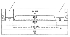
図2は、障壁層22上の保護層24の形成を示している。保護層24は、窒化珪素(SixNy)、窒化アルミニウム(AlN)、二酸化珪素(SiO2)、および/または他の適切な保護材料などの誘電体材料であってもよい。また、他の材料が保護層24に利用されてもよい。例えば、保護層24は、また、酸化マグネシウム、酸化スカンジウム、酸化アルミニウムおよび/または酸窒化アルミニウムを含んでもよい。さらに、保護層24は、単層であってもよく、または、均一組成および/または不均一組成の多層を含んでもよい。
FIG. 2 shows the formation of the
保護層24は、障壁層22の上に一面に形成されてもよい。例えば、保護層24は、高品質スパッタリングおよび/またはプラズマ増速化学気相成長法(PECVD)によって形成された窒化珪素(SiN)層であってもよい。保護層24は、約30nmの厚さである可能性があるが、他の厚さの層も利用されてもよい。例えば、保護層は、オーミックコンタクトの後のアニール中に下にある層を保護するように十分に厚くてもよい。そのような目的のために、2または3の単分子層程度の薄い層で十分である可能性がある。しかし、一般に、保護層24は、約10nmから約500nmの厚さを有する可能性がある。また、高品質SiN保護層は、III族窒化物層のMOCVD成長と共にその場(in−situ)成長されてもよい。
The
本発明の特定の実施形態では、保護層24はSiNであってもよい。SiN保護層は、PVDおよび/またはCVDによって形成されてもよく、圧縮または引っ張り歪みのために非化学量論的である可能性がある。例えば、SiN保護層は、約−100MPaから約100MPaの応力を受ける可能性がある。本発明のある特定の実施形態では、SiN保護層は、633nm波長で約1.6から約2.2の屈折率を有することがある。特定の実施形態では、SiN保護層の屈折率は、1.98±0.05であることがある。
In certain embodiments of the invention, the
図3は、障壁層22上へのオーミックコンタクト領域30の形成を示している。ここで図3を参照すると、保護層24は、障壁層22の部分を露出させるようにパターニングされ、第1および第2のオーミックコンタクト領域30が障壁層22上に形成される。例えば、下にある障壁層22を露出させるために、保護層24に窓がエッチングされてもよい。この窓は、パターニングされたマスクと障壁層22に対する低損傷エッチングとを利用して、エッチングされてもよい。低損傷エッチング技術の例には、誘導結合プラズマ、電子サイクロトロン共鳴(ECR)またはプラズマに対してDC成分のない下流プラズマエッチング(downstream plasma etching)などの、反応性イオンエッチング以外のエッチング技術が挙げられる。例えば、SiO2障壁層に対しては、緩衝フッ化水素酸を用いたウェットエッチングが使用されてもよい。ITO、SCO、MgOなどのエッチング停止層に対するSiNおよび/またはSiO2の選択エッチング、およびこれに続くエッチング停止層の低損傷除去が、行われてもよい。SiN障壁層の場合、SiO2がエッチング停止層として使用されてもよい。そのような実施形態では、保護層24は、エッチング停止層だけでなくSiN層、AlN層、および/またはSiO2層を含んでもよい。このように、本発明のある特定の実施形態では、保護層24は多層を含むことができる。
FIG. 3 shows the formation of the
依然として図3を参照すると、引き続いてフォトリソグラフィステップおよび蒸着を使用して、障壁層22の露出部分にオーミック金属が形成される。オーミック金属は、保護層24の窓よりも小さくなるようにパターニングされ、オーミック金属は第1および第2のオーミックコンタクト領域30を形成するようにアニールされる。そのようなものとして、オーミックコンタクト領域30の縁は近接した保護層24から間隔を空けて配置される可能性がある。
Still referring to FIG. 3, ohmic metal is subsequently formed in the exposed portions of the
アニールは、比較的高温のアニールであってもよい。例えば、アニールは、約900℃を超える温度で行われてもよい。そのようなオーミックコンタクトアニールを使用することによって、オーミックコンタクト領域30の抵抗は、比較的高抵抗から例えば約1Ω−mm未満に減少させることができる。したがって、本明細書で使用されるとき、用語「オーミックコンタクト」は、約1Ω−mm未満の接触抵抗を有する非整流性コンタクトを意味することができる。高温プロセスステップ中に保護層24が存在することで、そのようなステップで生じることがある障壁層22の損傷が減少し、かつ/または抑制されることがある。したがって、例えば、高温オーミックコンタクトアニール後のゲート領域21(すなわち、オーミックコンタクト領域30間のチャネルの長さ)のシート抵抗は、成長されたまま(すなわち、コンタクトアニール前)のゲート領域21のシート抵抗と実質的に同じである可能性がある。
The annealing may be a relatively high temperature annealing. For example, the anneal may be performed at a temperature above about 900 degrees Celsius. By using such an ohmic contact anneal, the resistance of the
オーミックコンタクト領域30は、オーミックコンタクト金属の形成および/またはパターニングでの位置合わせ不整合公差(misalignment torelance)を許容するのに十分な距離だけ保護層24から間隔を空けて配置される可能性がある。例えば、オーミックコンタクト領域30の端は、約0.1マイクロメートル(μm)から約0.2μmの距離だけ保護層24から間隔を空けて配置されることがある。その後の加熱ステップ中に金属が保護層24に拡散する可能性を減少させるために、オーミック金属と保護層24との接触を防ぐことが望ましい可能性があり、この金属拡散は、ゲートコンタクトとオーミックコンタクト領域30との間のショートをもたらすことがある。しかし、オーミックコンタクト領域30と保護層24との間の隙間は、保護層24の保護目的を駄目にするほど(かつ/またはデバイスの性能を実質的に悪くするほど)大きい必要はないが、オーミック材料と保護層24との間の接触のおそれがあるほど小さくてはいけない。したがって、本発明のある特定の実施形態では、この隙間は、約0.1マイクロメートル(μm)から約0.5μmの範囲であってもよい。
The
図4は、オーミックコンタクト領域30および保護層24の上への第2の層31の形成を示している。第2の層31は、保護層24よりも小さな誘電率を有する誘電体層であってもよい。例えば、第2の層31は、高温酸化物(HTO)層などの高品質酸化物層であってもよい。また、第2の層31は犠牲層であってもよく、この犠牲層は、後のステップで除去される可能性がある。例えば、第2の層31は、フォトレジスト層であってもよい。また、第2の層31は、ポリイミド層であってもよい。図4に示されるように、第2の層31は、第2の層31を貫通して保護層24の一部を露出させる孔またはリセス3を含む。例えば、第2の層31は、リセス3を形成するようにフォトリソグラフィでパターニングされてもよい。
FIG. 4 shows the formation of the
図5は、保護層24への開口または「窓」の形成を示し、その後のステップで、ここにゲート電極が形成されてもよい。図5に示されるように、開口4は、保護層24を貫通して障壁層22の一部を露出させるように形成される。より詳細には、開口4を形成するために、第2の層31をマスクとして使用して保護層24の露出部分がパターニングされる。障壁層22の露出表面への低漏れショットキーゲートコンタクトの形成を容易にするために、上述のように、第2の層31のリセス3によって露出された保護層24の部分を、低損傷エッチング技術を使用して選択的にエッチングすることによって、開口4が形成されてもよい。留意されたいことであるが、保護層24の開口4は、エッチングの等方性(すなわち、アンダーカット)のために第2の層31のリセス3よりも広くなる可能性がある。特定の実施形態では、オーミックコンタクト30はソースコンタクト及びドレインコンタクトを与えることができ、開口4が、したがってゲートコンタクトが、ドレインコンタクトよりもソースコンタクトに近くなるように、開口4がソースコンタクトとドレインコンタクトとの間で片寄っていることがある。
FIG. 5 shows the formation of an opening or “window” in the
ここで図6を参照すると、第2の層31のリセス3は、第1の開口4よりも広い第2の開口5を画定するように広くされる。そのようなものとして、第2の開口5は、第1の開口4と、第1の開口4の相対する側の保護層24の表面部を露出させる。第2の層31のリセス3は、第2の開口5と第1の開口4が自己整合されるように対称的に拡大されてもよい。例えば、第2の層31が保護層24と異なる材料で形成されている場合、第2の層31のリセス3は、ウェットエッチング技術を使用して第2の層31を選択的にエッチングすることによって広くされてもよい。より詳細には、第2の層31が酸化物層である場合、リセス3は、緩衝酸化物エッチング液(BOE)を使用して第2の層31を選択的にエッチングして広くされてもよい。その上または代替的に、第2の層31がフォトレジスト層である場合、酸素プラズマを使用して第2の層31をアッシングし、かつ/または、例えば摂氏100度(C)より高いが150度Cより低い温度で、デバイスをハードベークすることによって、このリセスが広くされてもよい。
Referring now to FIG. 6, the
したがって、図5および6に示されるように、第1の開口4を形成するために第2の層31をマスクとして使用して、保護層24が選択的にエッチングされてもよく、第2の層31のリセス3は、第2の開口5を形成するように第1の開口4のまわりで選択的に広くされてもよい。そのようなものとして、第1の開口4と第2の開口5は自己整合される可能性がある。いくつかの実施形態では、第2の層31は、保護層24に対して選択的にエッチング可能などんな材料であってもよい。
Thus, as shown in FIGS. 5 and 6, the
図7は、ゲート電極32の形成を示している。図7に示されるように、ゲート電極32は、第2の開口5および第1の開口4に形成され、保護層24を貫通して延在し、障壁層22の露出部分に接触する。ゲート電極32は、ゲート電極32と保護層24との間に隙間が形成されないように、保護層24の対向する側壁に直接に接して第1の開口4に形成されてもよい。適切なゲート材料は、障壁層24の組成に依存する可能性がある。しかし、ある特定の実施形態では、Ni、Pt、NiSix、Cu、Pd、Cr、TaN、Wおよび/またはWSiNなどの、窒化物ベースの半導体材料に対してショットキーコンタクトを作ることができる従来の材料が使用されてもよい。
FIG. 7 shows the formation of the
依然として図7を参照すると、ゲート電極32の第1の部分6(「ウィング」または「サイドローブ」とも呼ばれる。)は、第1の開口4の外側に存在する保護層24の表面部分で横方向に延在し、さらに、保護層24から縦方向に間隔を空けて配置されたゲート電極32の第2の部分7は、第2の開口5の外側に存在する第2の層31の表面部分で横方向に延在している。本明細書で使用されるとき、用語「横方向」は、基板の表面に対して実質的に平行な方向を意味する。ゲート電極32の第2の部分7は、第1の部分6を越えて横方向に延在してもよい。第1の開口4と第2の開口5は、これまで説明されたプロセスによって自己整合される可能性があるので、ゲート電極32の第1の部分6が保護層24上に延在する長さは、制御される可能性がある。そのようなものとして、本発明のいくつかの実施形態によると、ゲート電極32の保護層24上での延長によって生じる可能性があるトランジスタデバイスのゲート−ドレインキャパシタンス(cgd)および/またはゲート−ソースキャパシタンス(cgs)は、また、制御される可能性がある。したがって、自己整合サイドローブ6を備える修正ガンマゲート32が形成される可能性がある。
Still referring to FIG. 7, the first portion 6 (also referred to as “wing” or “sidelobe”) of the
図8は、犠牲的な第2の層31の除去を示している。図8に示されるように、第2の層31は、ゲート電極32が形成された後に除去される。第2の層31は、第2の層31の組成に応じて従来の技術を使用して形成されてもよい。
FIG. 8 shows the removal of the sacrificial
図9は、パシベーション層34の形成を示している。パシベーション層34は、トランジスタデバイスのための環境保護を行うことができる。例えば、パシベーション層34は、比較的厚い窒化物または比較的ローkの封入層であってもよく、保護層24の被覆率を改善するために形成されることがある。パシベーション層34は、第2の層31の除去後に、図8の構造の上に一面に堆積されてもよい。そのようなものとして、ゲート電極32の第2の部分7は、パシベーション層34の部分の上で横方向に延在する。特定の実施形態では、パシベーション層34は、保護層24とオーミックコンタクト30との間の隙間を実質的に埋めるように堆積されることがある。本発明のある特定の実施形態では、パシベーション層34は、窒化珪素、窒化アルミニウム、二酸化珪素、および/または酸窒化物であってもよい。さらに、パシベーション層34は、均一組成および/または不均一組成の単層または多層であってもよい。
FIG. 9 shows the formation of the
図10は、本発明のさらなる実施形態に従った高電子移動度トランジスタ(HEMT)デバイス100を示す断面図である。図10に示されるように、HEMTデバイス100のゲート電極32は、保護層24を貫通して延在し、障壁層22に接触している。ゲート電極32は、開口の外側に存在する保護層24の表面部分で横方向に延在する第1の部分6と、パシベーション層34によって保護層24から縦方向に間隔を空けて配置され、かつパシベーション層34の部分の上で第1の部分6を越えて横方向に延在する第2の部分7とを備える。言い換えると、ゲート電極32の第1および第2の部分6および7は、階段状外形を画定している。ゲート電極32の第2の部分7は、保護層24から約1000オングストローム(Å)から約6000Åだけ間隔を空けて配置されてもよい。ゲート電極32は、また、ゲート電極32と保護層24との間に隙間が存在しないように、保護層24の開口の対向する側壁に直接に接して延びている。ゲート電極32の第1の部分6は、また、保護層24上に直接に形成されてもよい。
FIG. 10 is a cross-sectional view illustrating a high electron mobility transistor (HEMT)
その上、(保護層24の中の)第1の開口および(図6の第2の層31の中の)第2の開口は、上述のプロセスによって自己整合される可能性があるので、第2の開口の幅(LG2として示される)は、第1の開口の幅のまわりに自己整合され、かつ対称である可能性があり、この第1の開口の幅がゲート長LG1を画定する。そのようなものとして、保護層24の開口の形成に基づいて関心のある動作周波数を得るように、ゲート長LG1が調整されてもよい。例えば、ゲート長LG1は、約0.05マイクロメートル(μm)から約2.0μmであってもよい。その上、ゲート電極32の第1の部分6が保護層24の上に延在する長さΔLGは、また、上述のように犠牲的な第2の層の開口を広くすることによって制御されてもよい。ピークゲート−ドレイン電圧VGDに確実に耐え、かつゲート−ドレインキャパシタンスcgdおよびゲート−ソースキャパシタンスcgsを最小限にし、かつ/または減少させるように、保護層24の厚さd1およびゲート電極32の第1の部分の長さΔLGが最適化されてもよい。例えば、長さΔLGは約0.1マイクロメートル(μm)から約0.6μmであってもよく、厚さd1は約300オングストローム(Å)から約5000Åであってもよい。その上、第1の開口を画定する保護層24の側壁の角度Φは、また、例えば、約45度から約90度の間で最適化されてもよい。
Moreover, since the first opening (in the protective layer 24) and the second opening (in the
上述のように、いくつかの実施形態では、保護層24はSiNであってもよく、障壁層22はAlGaNであってもよく、さらにチャネル層20はGaNであってもよい。上でも述べられたように、トランジスタ100は、また、基板10とチャネル層20の間に核形成層15を備える。
As described above, in some embodiments, the
また、図10は、オーミックコンタクト領域がソース/ドレインコンタクト領域30であってもよいことを示している。保護層24は、オーミックコンタクト領域と少なくともほぼ同じくらいの厚さに形成されてもよい。例えば、保護層24は、約500オングストローム(Å)から約5000Åの範囲の厚さに形成されてもよい。その上、パシベーション層34は、保護層24とソース/ドレイン領域30との間の隙間を実質的に埋めることができる。本発明のある特定の実施形態では、パシベーション層34は、保護層24と同じ材料で形成されてもよい。そのようなものとして、パシベーション層34は、窒化珪素、窒化アルミニウム、二酸化珪素および/または酸窒化物であってもよい。さらに、パシベーション層34は、均一組成および/または不均一組成の単層または多層であってもよい。
FIG. 10 also shows that the ohmic contact region may be the source /
本発明の他の実施形態では、第2の層31は犠牲層でなくてもよい。そのようなものとして、第2の層31は除去されなくてもよく、パシベーション層34は形成されなくてもよい。したがって、図7は、本発明の他の実施形態に従った高電子移動度トランジスタ(HEMT)デバイスを示している。例えば、上で言及されたように、第2の層31は誘電体層であってもよい。より詳細には、第2の層31は、HTO層および/または他の高品質酸化物層などの酸化物層であってもよく、さらに保護層24は、高純度窒化物(HPN)層などの窒化物層、および/または酸化物層に対して選択的にエッチング可能な他の保護層であってもよい。そのような酸化物層は、パシベーション層34に比較して低不純物濃度および/または他の改善された電気的特性を実現することができる。したがって、本発明のさらなる実施形態は、図11から18を参照して説明される。
In other embodiments of the present invention, the
図11から18は、本発明のさらなる実施形態に従ったトランジスタデバイスを作製する方法における中間(intermediate)作製ステップの例を示す断面図である。ここで図11を参照すると、図1を参照して上で説明されたように、トランジスタデバイスが形成されてもよい基板10に障壁層22およびチャネル層20が形成されてもよい。例えば、基板10は、半絶縁性炭化珪素(SiC)基板であってもよい。例えば、炭化珪素基板とデバイスの残りの部分との間に適切な結晶構造遷移をもたらすために、随意の緩衝層、核形成層および/または遷移層(図示せず)が基板10上に形成されてもよい。チャネル層20は、超格子等の単層または多層III族窒化物層であってもよい。障壁層22は、AlxGa1-xN(0<x<1)などのIII族窒化物層であってもよい。障壁層22は、また、AlInGaN、AlNおよび/またはこれらの層の組み合わせなどの他のIII族窒化物層も備えてもよい。
11 to 18 are cross-sectional views illustrating examples of intermediate fabrication steps in a method of fabricating a transistor device according to a further embodiment of the present invention. Referring now to FIG. 11, a
チャネル層20および障壁層22は、チャネル層と障壁層との間の界面がヘテロ接合を画定するように、異なるバンドギャップを有する材料で形成されてもよい。より詳細には、チャネル層20は、障壁層22のバンドギャップよりも小さなバンドギャップを有してもよい。例えば、チャネル層20及び障壁層22の両方がIII族窒化物層で形成されている場合、チャネル層20はGaN層であってもよく、障壁層22はAlGaN層であってもよい。さらに、チャネル層20および障壁層22は、異なる格子定数を有してもよい。例えば、それら2つの層の間の界面で障壁層22が「伸びる」ように、障壁層22は、チャネル層20よりも小さな格子定数を有する比較的薄い層であってもよい。したがって、擬似格子整合HEMT(pHEMT)デバイスが形成される可能性がある。
The
依然として図11を参照すると、保護層24が障壁層22上に形成されている。保護層24は、窒化珪素(SixNy)、窒化アルミニウム(AlN)、二酸化珪素(SiO2)、および/または他の適切な保護材料などの誘電体材料であってもよい。保護層24は、単層であってもよく、または、均一組成および/または不均一組成の多層を含んでもよい。また、他の材料が保護層24に利用されてもよい。
Still referring to FIG. 11, a
本発明のいくつかの実施形態では、保護層24は高純度窒化物(HPN)層であってもよい。本明細書で説明されるように、HPN層は、いくつかの他の窒化物層に比べてかなり低い全不純物レベルを有する窒化物層を意味することができる。より詳細には、HPN層の不純物レベルは、一般に、PECVDおよび/またはスパッタリングによって成長された窒化物層の不純物レベルよりも1桁から3桁小さい可能性がある。例えば、HPNは、Si3N4層と下の層との界面だけでなく、Si3N4層自体に比較的低い不純物濃度を有するほぼ化学量論的な窒化珪素(すなわち、Si3N4)を意味することができる。これは、下の層と同じ反応炉でHPN層を堆積し、かつ本明細書でさらに述べられる条件を使用することによって、達成される可能性がある。
In some embodiments of the present invention, the
例えば、保護層24は、特許文献18に記載されるような高純度SiN層を含んでもよく、この開示は、あたかも本明細書で完全に述べられたかのように参照して本明細書に組み込まれる。SiN層は、例えば、減圧化学気相成長法(LPCVD)および/または有機金属化学気相成長法(MOCVD)によって形成されてもよい。特に、本発明のある特定の実施形態に従って、SiN保護層24は、III族窒化物層のMOCVD成長と共にその場で(例えば、約700℃より高い)比較的高温で成長されてもよい。例えば、チャネル層20がGaNである場合、保護層24は、III族窒化物層の成長温度から基板10を冷やすことなくGaNエピタキシャル反応炉で成長されてもよい。特定の実施形態では、SiN層は、約900℃から約1000℃の範囲の温度で成長されてもよい。そのような高温成長はまた、SiN層の不純物レベル、およびIII族窒化物層とSiN層との間の界面の不純物レベルの減少を助長することができる。その上、SiN層に組み込まれるバックグラウンド反応炉不純物(background reactor impurity)のレベルの減少を助長することができる高成長速度が使用されてもよい。
For example, the
SiN層のその場形成は、また、一番上のIII族窒化物層の上面および/またはSiN層自体に組み込まれる不純物のレベルを減少させることができる。特に、デバイスが反応炉から取り出され、さらにSiN層が、例えばスパッタリングまたはPECVDのようなMOCVD後の成長プロセスによって形成されるとき、いくつかの異なるメカニズムで不純物が導入される可能性がある。例えば、特許文献19に詳細に述べられているように、III族窒化物層の成長中にMOCVD反応炉に水素が存在すると、成長に続く反応炉の冷却中に水素がIII族窒化物層に混入する傾向がある可能性がある。同様に、反応炉から取り出してすぐにデバイスを大気にさらすと、酸素原子の混入が可能になる場合がある。さらに、デバイスの取り扱いおよび/またはデバイスの化学洗浄の結果として、特にデバイスの外側表面の近接に、様々な他の不純物が取り込まれる可能性がある。ウェットエッチング、電極堆積、アニーリングステップなどの成長後処理が、SiN保護/パシベーション層の堆積前に行われる場合には、また、不純物が追加される可能性がある。望ましくない、かつ/または制御/再現し難い可能性のあるやり方で、これらの不純物は、III族窒化物層とSiN層との間の界面の表面状態を変える可能性がある。例えば、不純物が存在することで、SiN層と下のIII族窒化物層との間の界面での捕獲(trapping)が増加し、それによってチャネルのシート抵抗が高くなることがある。 In situ formation of the SiN layer can also reduce the level of impurities incorporated into the top surface of the top III-nitride layer and / or the SiN layer itself. In particular, when the device is removed from the reactor and the SiN layer is formed by a post-MOCVD growth process such as sputtering or PECVD, impurities can be introduced by several different mechanisms. For example, as described in detail in U.S. Patent No. 6,053,099, if hydrogen is present in the MOCVD reactor during the growth of the III nitride layer, the hydrogen is transferred to the III nitride layer during the reactor cooling following the growth. May have a tendency to mix. Similarly, exposure of the device to the atmosphere immediately after removal from the reactor may allow oxygen atoms to be incorporated. In addition, various other impurities may be incorporated, particularly in the vicinity of the outer surface of the device, as a result of device handling and / or chemical cleaning of the device. Impurities may also be added if post-growth processes such as wet etching, electrode deposition, annealing steps, etc. are performed prior to deposition of the SiN protection / passivation layer. In ways that may be undesirable and / or difficult to control / reproduce, these impurities can change the surface state of the interface between the III-nitride layer and the SiN layer. For example, the presence of impurities may increase trapping at the interface between the SiN layer and the underlying III-nitride layer, thereby increasing the channel sheet resistance.
本発明のある特定の実施形態では、窒化珪素層は、高純度シリコンガス(例えば、純度99.99%)供給源を使用して形成されてもよい。例えば、高純度シラン(SiH4)が、SiN層の成長で供給源ガスとして使用されてもよい。当業者には知られているように、シランは、n型ドープIII族窒化物層の成長において、シリコンドーパントの供給源としてしばしば使用される。一般に、希釈シランガスは、純粋シランよりも高価でなくかつ使用し易いので、そのような用途に使用され、純粋シランは非常に燃えやすい可能性がある。そのような純粋シランを使用することで、例えば、III族窒化物層とSiN層との界面および/またはSiN層中の不純物のレベルを減少させることが容易になる可能性があり、このことは、ある特定の環境で、デバイスの性能および/または再現性を改善する可能性がある。特に、より高品質の(すなわち、より純粋な)SiN層は、絶縁層の本体中の捕獲を減少させ、または最小限にするのに役立ち、それによってより高い破壊臨界電界を可能にする可能性がある。純粋ジシラン(Si2H6)または他の純粋シリコンガス供給源が、高純度シラン(SiH4)の代わりに使用されてもよい。そのような純粋シランガス供給源が反応炉に含まれるとき、例えばn型ドープまたはコドープ(co−doped)III族窒化物層の成長中に希釈シランガスをドーパントガス供給源として使用することができるように、希釈シラン供給源も含むことがいっそう望ましい可能性がある。 In certain embodiments of the invention, the silicon nitride layer may be formed using a high purity silicon gas (eg, 99.99% purity) source. For example, high purity silane (SiH 4 ) may be used as the source gas in the growth of the SiN layer. As is known to those skilled in the art, silane is often used as a source of silicon dopant in the growth of n-type doped group III-nitride layers. In general, diluted silane gas is less expensive and easier to use than pure silane, so it is used in such applications, and pure silane can be very flammable. By using such pure silanes, for example, it may be easier to reduce the level of impurities in the interface between the group III nitride layer and the SiN layer and / or in the SiN layer, May improve device performance and / or reproducibility in certain circumstances. In particular, a higher quality (ie, purer) SiN layer may help reduce or minimize trapping in the body of the insulating layer, thereby allowing a higher breakdown critical field There is. Pure disilane (Si 2 H 6 ) or other pure silicon gas source may be used instead of high purity silane (SiH 4 ). When such a pure silane gas source is included in the reactor, for example, dilute silane gas can be used as a dopant gas source during the growth of an n-type doped or co-doped III-nitride layer. It may be even more desirable to include a diluted silane source.
いくつかの実施形態では、高純度SiN層24は、化学量論的である可能性がある。用語「化学量論」は、化学量論的化合物中の元素のモル比を意味することができる。そのような化学量論的化合物では、モル比は整数である。例えば、Si3N4におけるシリコンおよび窒素の化学量論は、約3:4である。SiN層の化学量論は、また、この層の屈折率に影響を及ぼす可能性がある。本発明のある特定の実施形態では、SiN保護層24は、633nmの波長で約1.6から約2.2の屈折率を有することがある。化学量論的SiNは、また、緩衝酸化物エッチング液(BOE)で比較的小さなエッチング速度を特徴とする可能性がある。例えば、化学量論的SiNのBOEでのエッチング速度は、約10オングストローム/分よりも小さいことがある。対照的に、PECVD窒化珪素は、約100オングストローム/分のオーダのBOEエッチング速度を有することがあり、スパッタ窒化珪素は、約1000オングストローム/分以上のオーダのBOEエッチング速度を有することがある。SiN層の化学量論は、例えば、CVDプロセスにおいてSiH4およびNH3の供給源ガスの相対的な流速を調整することによって、調整されてもよい。さらに、比較的高温で形成されるとき、CVD成長のSiNは化学量論的である傾向がある。
In some embodiments, the high
本発明のいくつかの実施形態では、保護層24は、その後の高温プロセスステップ時の障壁層22への損傷を減少させ、かつ/または妨げるように、十分に厚いHPN層を含んでもよい。例えば、HPN層22は、約200オングストローム(Å)から約2000Åの厚さを有してもよい。さらに、保護層24は、HPNおよび二酸化珪素(SiO2)および/またはプラズマ化学気相成長(PECVD)窒化珪素(SiN)の多層を含んでもよい。理解されることであろうが、用語「SixNy」、「SiN」および「窒化珪素」は、本明細書では、化学量論的窒化珪素と非化学量論的窒化珪素の両方を意味するように交換可能に使用される。しかし、本発明の実施形態は、これらの例によって限定されず、例えば、どんなHPNでも高品質誘電体保護層24として使用されることがある。もっと一般的に、保護層24の材料は、適切な界面特性を持つべきであり、比較的高温に耐えることができるべきであり、さらに、下にある障壁層22を大きく損傷することなく除去可能であるべきである。
In some embodiments of the present invention, the
図12は、保護層24上への酸化物層33などの誘電体層の形成を示している。例えば、酸化物層33は、約500℃を超える温度の化学気相成長(CVD)プロセスを使用して保護層24上に堆積されてもよい。その上かつ/または代わりに、酸化物層33は、その場形成されてもよい。酸化物層33は、保護層24の厚さよりも大きな厚さに形成されてもよい。例えば、酸化物層33は、約300オングストローム(Å)から約5000Åの厚さを有してもよい。
FIG. 12 shows the formation of a dielectric layer such as an
酸化物層33はまた、保護層24よりも小さな誘電率を有する可能性がある。例えば、酸化物層33は、高温酸化物(HTO)層等の高品質酸化物層であってもよい。高品質酸化物層33は、約1.5未満の誘電定数または誘電率を有する可能性がある。さらに、高品質酸化物層33は比較的低不純物濃度を有する可能性があり、これは例えば、二次イオン質量スペクトロスコピー(SIMS)分析によって測定されることがある。そのようなものとして、本発明のいくつかの実施形態に従った高品質酸化物層は、図10のゲート後パシベーション層34などのPECVDプロセスによって形成された層に比べて改善された電気特性を有している可能性がある。
The
例えば、いくつかの実施形態では、HTO層は、約900℃の温度のLPCVDプロセスで堆積された二酸化珪素(SiO2)層であってもよい。この堆積のLPCVDの性質によって、下の半導体層に及ぼすマイナスの影響を減らしながら、かつ/または最小限にしながら酸化物層33を形成することができるようになることがある。さらに、堆積が比較的高温であることで、約8〜9MV/cmの測定絶縁耐力(measured dielectric strength)(すなわち、SiO2の理論値の約80〜90%)を有する比較的高密度の酸化物層33の形成が可能になることがある。
For example, in some embodiments, the HTO layer may be a silicon dioxide (SiO 2 ) layer deposited by an LPCVD process at a temperature of about 900 ° C. The LPCVD nature of this deposition may allow the
本発明のある実施形態では、酸化物層33は、化学量論的SiO2であってもよい。このSiO2層は、633nmの波長で約1.36から約1.56の屈折率を有することがある。特定の実施形態では、SiO2保護層の屈折率は、偏光解析法で測定された場合に1.46±0.03であることがある。さらに、このSiO2層は、電荷、トラップ、および他の電気的に活性な非理想的性質(不純物)のレベルの減少を実現することができ、これは、ある特定の環境で、デバイスの性能および/または再現性を改善する可能性がある。特に、高品質の(すなわち、いっそう純粋な)SiO2層は、絶縁層の本体中の捕獲を減少させるか、最小限にするのに役立ち、それによっていっそう高い破壊臨界電界を可能にする可能性がある。もっと一般的に、酸化物層33は、HEMTデバイスのゲート−ドレインおよび/またはゲート−ソースキャパシタンスを減少させるのに十分である可能性のある厚さ、不純物濃度、誘電率および/または他の特性を与えるように選ばれてもよい。
In some embodiments of the invention, the
ここで図13を参照すると、酸化物層33および保護層24は、障壁層22の部分を露出させるようにパターニングされている。例えば、保護層24の第1および第2の部分を露出させるリセス9を画定するために、パターンニングされたマスク(図示せず)を利用して酸化物層33がパターニングされてもよく、さらに、障壁層22の部分を露出させる窓8を画定するために、酸化物層33をマスクとして利用して保護層24がパターニングされてもよい。より詳細には、酸化物層33にリセス9を画定するためにドライエッチングプロセスが使用されてもよく、窓8を画定するように保護層24を選択的にエッチングするために、低損傷ウェットエッチングプロセスが使用されてもよい。ITO、SCO、MgOなどのエッチング停止層までの保護層24の選択エッチング、その後に続くエッチング停止層の低損傷除去が、また、行われてもよい。そのような実施形態では、保護層24は、エッチング停止層だけでなくSiN層、AlN層、および/またはSiO2層を含むことがある。あるいは、層33と24の両方が堆積された状態で、酸化物層33と保護層24の両方を通して単一ステップでエッチングするために、低損傷ドライエッチングが使用されてもよい。そのような低損傷エッチング技術の例には、誘導結合プラズマエッチングまたは電子サイクロトロン共鳴(ECR)エッチングまたはプラズマに対してDC成分のない下流プラズマエッチングなどの反応性イオンエッチング以外のエッチング技術がある可能性がある。
Referring now to FIG. 13, the
また、いくつかの実施形態では、保護層24は、酸化物層33を形成する前に、障壁層22の部分を露出させる窓8を画定するようにパターニングされてもよい。そのようなものとして、酸化物層は、保護層24の上に、さらに障壁層22の第1および第2の部分の上に形成されてもよい。酸化物層は、次に、障壁層22の部分を露出させるリセス9を画定するようにパターニングされてもよい。リセス9は、保護層24にエッチングされた窓8よりも狭くてもよい。そのようなものとして、保護層24の窓8の側壁に沿って酸化物層33の部分が残っている可能性がある。したがって、次のステップで、オーミックコンタクト領域が障壁層22に形成されたとき、オーミックコンタクト領域と保護層24との間に酸化物層33が存在するために、オーミックコンタクト領域の縁は、近接した保護層24から間隔を空けて配置されている可能性がある。
Also, in some embodiments, the
図14は、障壁層24へのオーミックコンタクト30の形成を示している。ここで図14を参照すると、障壁層22にオーミック金属領域を形成するために、窓8およびリセス9によって露出された障壁層22の部分に、蒸着によって金属が堆積されもよい。適切な金属には、チタン(Ti)、タングステン(W)、チタンタングステン(TiW)、シリコン(Si)、窒化チタンタングステン(TiWN)、タングステンシリサイド(WSi)、レニウム(Re)、ニオブ(Nb)、ニッケル(Ni)、金(Au)、アルミニウム(Al)、タンタル(Ta)、モリブデン(Mo)、ニッケルシリサイド(NiSi)、チタンシリサイド(TiSi)、窒化チタン(TiN)、窒化タングステンシリコン(WSiN)、白金(Pt)などの耐熱金属がある可能性がある。どんな不要な金属も、例えば溶媒を使用して除去されてもよい。オーミック金属領域は、保護層24の窓よりも小さくなるようにパターニングされてもよく、さらに、第1および第2のオーミックコンタクト領域30を形成するようにアニールされてもよい。そのようなものとして、オーミックコンタクト領域30は、オーミックコンタクト金属の形成および/またはパターニングでの位置合わせ不良公差(misalignment tolerance)を許容するのに十分な距離だけ保護層24から間隔を空けて配置される可能性がある。例えば、オーミックコンタクト領域30の縁は、約0.1マイクロメートル(μm)から約0.5μmの距離だけ保護層24から間隔を空けて配置されてもよい。
FIG. 14 shows the formation of the
依然として図14を参照すると、アニールは比較的高温のアニールであってもよい。例えば、アニールは、約900℃を超える温度で行われてもよい。そのようなオーミックコンタクトアニールを使用することによって、オーミックコンタクト領域30の抵抗は、比較的高い抵抗から例えば約1Ω−mm未満に減少することがある。したがって、本明細書で使用されるとき、用語「オーミックコンタクト」は、約1Ω−mm未満の接触抵抗を有する非整流性コンタクトを意味することができる。高温プロセスステップ中に保護層24が存在することで、そのようなステップで生じることがある障壁層22への損傷が減少し、かつ/または妨げられる可能性がある。したがって、例えば、高温オーミックコンタクトアニール後のゲート領域21(すなわち、オーミックコンタクト領域30間のチャネル長さ)のシート抵抗は、成長されたまま(すなわち、コンタクトアニール前)のゲート領域21のシート抵抗と実質的に同じである可能性がある。
Still referring to FIG. 14, the anneal may be a relatively high temperature anneal. For example, the anneal may be performed at a temperature above about 900 degrees Celsius. By using such an ohmic contact anneal, the resistance of the
理解されることであろうが、いくつかの実施形態では、オーミックコンタクト30を形成するために、堆積された金属をアニールすることは必要でないことがある。例えば、障壁層22の注入ソース/ドレイン領域にオーミックコンタクト30が形成される場合、金属は、堆積されたままでオーミックであることがある。コンタクトアニールは必要でない可能性があるので、オーミックコンタクト30の金属が保護層24に接触することは許容できることがある。したがって、本発明のいくつかの実施形態では、オーミックコンタクト30が保護層24から確実に間隔を空けて配置されるようにするために、さもなれれば、必要とされることがあるリソグラフィステップは、障壁層22中への不純物注入の結果として、回避される可能性がある。その上、オーミックコンタクト30は、注入領域に形成されてもよいので、このオーミックコンタクトは、非注入領域に形成されたオーミックコンタクトよりも低い抵抗率を有している可能性がある。したがって、本発明のいくつかの実施形態に従って形成されたデバイスのオン抵抗は、小さくなる可能性がある。さらに、本発明のいくつかの実施形態は、特許文献20及び21に述べられているような半導体作製方法を使用することができる。これらの開示は、参照してその全体が本明細書に組み込まれる。
As will be appreciated, in some embodiments, it may not be necessary to anneal the deposited metal to form the
図15は、酸化物層33への孔またはリセス3の形成を示している。より詳細には、オーミックコンタクト30および酸化物層33の上にマスク(図示せず)が形成され、リセス3を形成するように酸化物層33がパターニングされる。酸化物層33は、例えば、上述のエッチング技術の1つによって選択的にパターニングされてもよい。リセス3は、酸化物層33を貫通して延在し、保護層24の一部を露出させる。
FIG. 15 shows the formation of holes or recesses 3 in the
図16は、次のステップでゲート電極が形成されてもよい保護層24の開口または「窓」の形成を示している。図16に示されるように、開口4は、障壁層22の一部を露出させるように保護層24を貫通して形成される。より詳細には、開口4を形成するために、酸化物層33をマスクとして使用して保護層24の露出部分がパターニングされる。酸化物層33のリセス3によって露出された保護層24の部分を、上述のように低損傷エッチング技術を使用して選択的にエッチングすることによって、開口4は形成され、それによって、障壁層22の露出表面への低漏れ(low−leakage)ショットキーゲートコンタクトの形成を容易にすることができる。留意されたいことであるが、このエッチングの等方性(すなわち、アンダーカット)のために、保護層24の開口4は、酸化物層33のリセス3よりも広くなる可能性がある。特定の実施形態では、オーミックコンタクト30は、ソースコンタクトおよびドレインコンタクトを与えることができ、開口4が、また後でゲートコンタクトが、ドレインコンタクトよりもソースコンタクトに近くなるように、開口4は、ソースコンタクトとドレインコンタクトの間で片寄っていてもよい。
FIG. 16 illustrates the formation of an opening or “window” in the
理解されるべきことであるが、いくつかの実施形態では、障壁層22を露出させるように酸化物層33のリセス3および保護層24の開口4を画定するために、酸化物層33と保護層24の両方を通して単一ステップでエッチングするように低損傷ドライエッチングが使用されてもよい。その上、いくつかの実施形態では、酸化物層33および保護層24は、単一マスクを使用してリセス3および9ならびに開口4および8を画定するようにパターニングされてもよい。もっと一般的には、いくつかのステップは、特定の中間作製ステップを参照して図示され、説明されたが、本発明の特定の実施形態では、組み合わされ、分割され、かつ/または削除されてもよい。
It should be understood that in some embodiments, the
ここで図17を参照すると、酸化物層33のリセス3は、第1の開口4よりも広い第2の開口5を画定するように広くされている。そのようなものとして、第2の開口5は、第1の開口4と、第1の開口4の相対する側の保護層24の表面部分を露出させる。酸化物層33のリセス3は、第2の開口5と第1の開口4が自己整合されるように対称的に広げられてもよい。例えば、酸化物層33のリセス3は、緩衝酸化物エッチング液(BOE)を使用して酸化物層33を選択的にエッチングすることによって広くされてもよい。さらに、いくつかの実施形態では、オーミックコンタクト30の形成で使用される酸化物層33のリセス9は、また、緩衝酸化物エッチング液(BOE)によって対称的に広げられてもよい。
Referring now to FIG. 17, the
したがって、図16および17に示されるように、保護層24は、第1の開口4を形成するために酸化物層33をマスクとして使用して選択的にエッチングされてもよく、酸化物層33のリセス3は、第2の開口5を形成するように第1の開口4のまわりに選択的に広くされてもよい。そのようなものとして、第1の開口4と第2の開口5は、自己整合される可能性がある。いくつかの実施形態では、酸化物層33は、保護層24に対して選択的にエッチングされる可能性のある他の高品質誘電体材料で形成されてもよい。
Accordingly, as shown in FIGS. 16 and 17, the
図18は、本発明のさらなる実施形態に従った高電子移動度トランジスタ(HEMT)デバイス200を実現するためのゲート電極32の形成を示している。図18に示されるように、オーミックコンタクト領域は、ソース/ドレインコンタクト領域30であることがある。また、ゲート電極32は、第2の開口5および第1の開口4に形成され、保護層24を貫通して障壁層22の露出部分に接触している。ゲート電極32は、保護層24とゲート電極32の間に隙間が形成されないように、第1の開口の中の保護層24の対向する側壁に直接に形成されてもよい。その上および/または代わりに、高品質二酸化珪素ライナまたは窒化物ライナなどの誘電体ライナ(図示せず)が、第1の開口の中の保護層24の対向する側壁に形成されてもよい。金属−絶縁体−半導体(MIS)HEMTデバイスを形成するように、ゲート電極32が誘電体ライナに直接に形成されてもよい。
FIG. 18 illustrates the formation of a
適切なゲート材料は、障壁層24の組成に依存する可能性がある。しかし、ある特定の実施形態では、窒化物ベースの半導体材料に対してショットキーコンタクトを作ることができる従来の材料、Ni、Pt、NiSix、Cu、Pd、Cr、TaN、Wおよび/またはWSiNなどが、使用されてもよい。さらに、いくつかの実施形態では、ゲート材料は、また、ゲート電極32の形成中にソース/ドレインコンタクト領域30に堆積されてもよい。より詳細には、ゲート材料は、保護層24の第1の開口4の中に、および酸化物層33の第2の開口5およびリセス9の中に堆積されてもよい。次に、ゲート材料は、ゲート材料の部分がリセス9のソース/ドレインコンタクト領域30上に残ったままになるようなやり方でゲート電極32を画定するように、パターニングされてもよい。ソース/ドレインコンタクト領域30上にゲート材料(または、他の導電材料)を形成することで、例えばプローブアクセス(probe access)および/またはワイヤボンディングのために、比較的小さなソース/ドレインコンタクト領域30への接触が容易になる可能性がある。
A suitable gate material may depend on the composition of the
依然として図18を参照すると、ゲート電極32の第1の部分6(「ウィング」または「サイドローブ」とも呼ばれる。)は、第1の開口4の外側に存在する保護層24の表面部分で横方向に延在し、さらに保護層24から縦方向に間隔を空けて配置されたゲート電極32の第2の部分7は、第2の開口5の外側に存在する酸化物層33の部分の上で横方向に延在している。本明細書で使用されるとき、用語「横方向」は、基板の表面に対して実質的に平行な方向を意味する。ゲート電極32の第2の部分7は、第1の部分6を越えて横方向に延在してもよい。言い換えると、ゲート電極32の第1および第2の部分6および7は、階段状外形を画定する。したがって、自己整合(self−aligned)サイドローブ6を有する(modified)修正ガンマゲート32が形成される可能性がある。
Still referring to FIG. 18, the first portion 6 (also referred to as “wing” or “sidelobe”) of the
また、図18に示されるように、上述のように酸化物層33の開口を広くすることによって、第1の開口4と第2の開口5は自己整合される可能性があるので、ゲート電極32の第1の部分6が保護層24上に延在する長さΔLGは制御される可能性がある。さらに、ゲート電極32の第2の部分7は、酸化物層33の厚さに基づいて、保護層24から間隔を空けて配置される可能性がある。そのようなものとして、本発明のいくつかの実施形態によると、ゲート電極32の保護層24上への延長によって生じる可能性があるトランジスタデバイスのゲート−ドレインキャパシタンス(cgd)および/またはゲート−ソースキャパシタンス(cgs)もまた、制御される可能性がある。高品質酸化物層33の比較的小さな誘電率は、ゲート−ドレインおよび/またはゲート−ソースキャパシタンスの減少にさらに寄与する可能性がある。
Also, as shown in FIG. 18, since the first opening 4 and the
ピークゲート−ドレイン電圧VGDに確実に耐えるように、かつ/またはゲート−ドレインキャパシタンスcgdおよび/またはゲート−ソースキャパシタンスcgsを最小限にしかつ/または減少させるように、保護層24の厚さd1およびゲート電極32の第1の部分の長さΔLGが、また、最適化されてもよい。例えば、長さΔLGは、約0.1マイクロメートル(μm)から約0.6μmであってもよく、厚さd1は約200オングストローム(Å)から約2000Åであってもよい。さらに、酸化物層33の厚さd2は、約500オングストローム(Å)から約3000Åであってもよい。第1の開口を画定する保護層24の側壁の角度φは、また、例えば約45度から約90度の間で、最適化されてもよい。また、(LG2として示されている)第2の開口の幅は、ゲート長LG1を画定する第1の開口の幅のまわりに自己整合され、対称である。そのようなものとして、ゲート長LG1は、保護層24への開口の形成に基づいて、関心のある動作周波数を得るように調整されてもよい。例えば、ゲート長LG1は、約0.05マイクロメートル(μm)から約2.0μmであってもよい。
The thickness of the
したがって、本発明のいくつかの実施形態は、Tゲートの肯定的特性の多くを誘電的に支持されたゲート電極、またはガンマゲートの肯定的特性と組み合わせることができる。したがって、自己整合ウィング/サイドローブを有する修正ガンマゲート構造が、比較的小さなゲート抵抗、比較的小さなゲート−ドレインおよび/またはゲート−ソースキャパシタンス、および比較的高い利得を有するように実現される。さらに、ゲート電極と保護層との間の隙間は、減少され、かつ/または生じないようにされる可能性があり、ピーク電界は減少される可能性がある。 Thus, some embodiments of the present invention can combine many of the positive characteristics of T-gates with the positive characteristics of dielectric supported gate electrodes, or gamma gates. Thus, a modified gamma gate structure with a self-aligned wing / sidelobe is realized with a relatively small gate resistance, a relatively small gate-drain and / or gate-source capacitance, and a relatively high gain. Furthermore, the gap between the gate electrode and the protective layer may be reduced and / or prevented from occurring, and the peak electric field may be reduced.
本発明の実施形態を特定のHEMT構造を参照して本明細書で説明したが、本発明は、そのような構造に限定されるものと解釈すべきでなく、擬似格子整合HEMT(pHEMT)(GaAs/AlGaAs pHEMTを含む)および/またはGaN MESFETなどの多くの異なるトランジスタ構造のゲート電極の形成に応用してもよい。より一般的に、ゲート電極が形成される可能性があり、かつ/または成長されたままの表面特性の維持が絶対必要である可能性がある電子デバイスのいずれにおいても、本発明の実施形態を応用してもよい。例えば、窒化珪素および/またはその他の除去可能な封入剤を、AlGaN金属−半導体−金属(MSM)検出器、RFリミッタダイオード構造、および/または電力スイッチングショットキーダイオードの作製シーケンスにおいて使用することが可能である。 Although embodiments of the present invention have been described herein with reference to particular HEMT structures, the present invention should not be construed as limited to such structures, and is not limited to such a pseudo-lattice matched HEMT (pHEMT) ( It may be applied to the formation of gate electrodes of many different transistor structures such as GaAs / AlGaAs pHEMT) and / or GaN MESFETs. More generally, embodiments of the present invention can be used in any electronic device where a gate electrode may be formed and / or maintenance of surface properties as grown may be absolutely necessary. You may apply. For example, silicon nitride and / or other removable encapsulants can be used in the fabrication sequence of AlGaN metal-semiconductor-metal (MSM) detectors, RF limiter diode structures, and / or power switching Schottky diodes. It is.
また、依然として本発明の教示の恩恵を受けながら、トランジスタデバイスに追加の層が含まれることがある。そのような追加の層には、例えば、非特許文献1または特許文献5に記載されるようなGaNキャップ層がある可能性があり、これらの開示は、あたかも本明細書で完全に述べられたかのように参照して組み込まれる。いくつかの実施形態では、SiNxのような絶縁層、または比較的高品質のAlNが、MISHEMTを作るために、かつ/または表面にパシベーション膜を被せるために、堆積されることがある。これらの追加の層は、また、1つまたは複数の組成傾斜遷移層を含むことがある。さらに、上述の障壁層22は多層を含むことがある。したがって、本発明の実施形態は、障壁層を単一層に限定するように解釈されるべきでなく、例えば、GaN層、AlGaN層および/またはAlN層の組み合わせを有する障壁層を含むことができる。例えば、GaN、AlN構造が、合金散乱を減少させ、または防ぐために利用されることがある。
Also, additional layers may be included in the transistor device while still benefiting from the teachings of the present invention. Such additional layers may include, for example, a GaN cap layer as described in
図面および明細書で本発明の代表的な実施形態が開示され、また、特定の用語が使用されたが、これらの用語は、一般的な記述的な意味でだけ使用され、限定する目的に使用されていない。 While representative embodiments of the present invention are disclosed in the drawings and specification and specific terms are used, these terms are used only in a general descriptive sense and are used for limiting purposes. It has not been.
Claims (46)
前記チャネル層上に障壁層を形成するステップと、
前記障壁上に保護層を形成するステップであって、前記保護層は、前記保護層を貫通して延在する第1の開口を有するステップと、
前記保護層が第1と第2のオーミックコンタクト領域の間にあるように、前記保護層に近接しかつ前記保護層から間隔を空けて配置された前記第1および第2のオーミックコンタクト領域を前記障壁層上に形成するステップと、
前記保護層上に第2の層を形成するステップであって、前記第2の層は、前記第2の層を貫通して延在する第2の開口を有し、前記第1および第2の開口が自己整合されるステップと、
前記第1および第2の開口にゲート電極を形成するステップと
を含み、
前記第2の開口は、前記第1の開口よりも広く、ゲート電極の第1の部分が、前記第1の開口の外側に存在する前記保護層の表面部分で横方向に延在し、かつ、前記保護層から間隔を空けて配置された前記ゲート電極の第2の部分が、前記第1の部分を越えて、前記第2の開口の外側に存在する前記第2の層の部分で横方向に延在し、
前記第1の開口の幅は、傾斜することによって前記障壁層から前記第2の層に向かって大きくなることを特徴とするトランジスタを作製する方法。Forming a channel layer;
Forming a barrier layer on the channel layer;
Forming a protective layer on the barrier, the protective layer having a first opening extending through the protective layer;
The first and second ohmic contact regions disposed adjacent to and spaced from the protective layer such that the protective layer is between the first and second ohmic contact regions. Forming on the barrier layer;
Forming a second layer on the protective layer, wherein the second layer has a second opening extending through the second layer, the first and second A step of self-aligning the opening of
Forming a gate electrode in the first and second openings,
The second opening is wider than the first opening, the first portion of the gate electrode extends laterally at the surface portion of the protective layer present outside the first opening; and A second portion of the gate electrode spaced apart from the protective layer is transverse to the portion of the second layer that is outside the second opening beyond the first portion. Extending in the direction,
A method for manufacturing a transistor, wherein the width of the first opening increases from the barrier layer toward the second layer by being inclined .
前記第2の層を貫通して前記保護層の一部を露出させるリセスを含む前記第2の層を前記保護層上に形成するステップと、
前記第1の開口を露出させ、かつ前記第1の開口の相対する側に前記保護層の表面部分を露出させる前記第2の開口を画定するように、前記第2の層の前記リセスを広くするステップと
を含むことを特徴とする請求項3に記載の方法。Forming the second layer having the second opening existing through the second layer;
Forming the second layer on the protective layer including a recess penetrating the second layer to expose a portion of the protective layer;
The recess in the second layer is widened so as to define the second opening exposing the first opening and exposing a surface portion of the protective layer on the opposite side of the first opening. The method of claim 3, further comprising the step of:
酸素プラズマを使用して前記第2の層をアッシングするステップ、および/または前記第2の層をハードベークするステップを含むことを特徴とする請求項7に記載の方法。Widening the recess in the second layer comprises:
8. The method of claim 7, comprising ashing the second layer using an oxygen plasma and / or hard baking the second layer.
前記開口の中の前記保護層の対向する側壁に直接に前記ゲート電極を形成するステップを含むことを特徴とする請求項1に記載の方法。Forming the gate electrode comprises:
The method of claim 1, comprising forming the gate electrode directly on opposing sidewalls of the protective layer in the opening.
前記障壁層の部分を露出させるように前記保護層をパターニングするステップと、
前記パターニングされた保護層に近接し、かつ前記パターニングされた保護層から間隔を空けて配置されたオーミック金属領域を前記障壁層の前記露出部分に形成するステップと、
前記オーミック金属領域をアニールするステップと
を含むことを特徴とする請求項1に記載の方法。Forming the first and second ohmic contact regions comprises:
Patterning the protective layer to expose portions of the barrier layer;
Forming an ohmic metal region in the exposed portion of the barrier layer proximate to the patterned protective layer and spaced from the patterned protective layer;
2. The method of claim 1, comprising annealing the ohmic metal region.
前記酸化物層を貫通して前記保護層の一部を露出させるリセスを含む前記誘電体層を前記保護層上に形成するステップと、
前記保護層を貫通して延在する前記第1の開口を形成するために、前記誘電体層をマスクとして使用して前記保護層をパターニングするステップと、
前記第1の開口を露出させ、かつ前記第1の開口の相対する側に前記保護層の表面部分を露出させる前記第2の開口を画定するように、前記酸化物層の前記リセスを広くするステップと
を含み、
前記保護層および前記酸化物層は異なる材料を備え、前記酸化物層の前記リセスを広くするステップは、ウェット酸化物エッチング液を使用して前記酸化物層をエッチングすることによって、前記第2の開口と前記第1の開口が自己整合されるように、前記酸化物層の前記リセスを対称的に広げるステップを含み、前記ウェット酸化物エッチング液は、前記保護層に対して選択であることを特徴とする請求項15に記載の方法。Forming the oxide layer having the second opening extending through the oxide layer comprises:
Forming the dielectric layer on the protective layer including a recess penetrating the oxide layer to expose a portion of the protective layer;
Patterning the protective layer using the dielectric layer as a mask to form the first opening extending through the protective layer;
The recess of the oxide layer is widened to define the second opening exposing the first opening and exposing a surface portion of the protective layer on the opposite side of the first opening. Including steps,
The protective layer and the oxide layer comprise different materials, and the step of widening the recess of the oxide layer comprises etching the oxide layer using a wet oxide etchant. Symmetrically widening the recess of the oxide layer such that an opening and the first opening are self-aligned, wherein the wet oxide etchant is selective to the protective layer The method according to claim 15, characterized in that:
前記酸化物層および前記保護層をパターニングした後で、前記保護層が第1と第2のオーミックコンタクト領域の間にあるように、前記パターニングされた保護層に近接しかつ前記パターニングされた保護層から間隔を空けて配置された前記第1および第2のオーミックコンタクト領域を、前記障壁層の前記第1および第2の部分にそれぞれ形成するステップと
を含むことを特徴とする請求項15に記載の方法。Patterning the oxide layer and the protective layer to expose first and second portions of the barrier layer;
After patterning the oxide layer and the protective layer, the patterned protective layer is proximate to the patterned protective layer and is between the first and second ohmic contact regions. Forming the first and second ohmic contact regions spaced apart from each other in the first and second portions of the barrier layer, respectively. the method of.
前記酸化物層を形成するステップの前に、前記障壁層の前記第1および第2の部分を露出させるように前記保護層をパターニングするステップであって、前記酸化物層を形成するステップは、前記保護層上、ならびに前記障壁層の前記第1および第2の部分上に前記酸化物層を形成するステップを含むステップと、
前記障壁層の前記第1および第2の部分をそれぞれ露出させる第1および第2のリセスを前記酸化物層に画定するように前記酸化物層をパターニングするステップと
を含むことを特徴とする請求項23に記載の方法。Patterning the oxide layer and the protective layer comprises:
Patterning the protective layer to expose the first and second portions of the barrier layer prior to forming the oxide layer, the forming the oxide layer comprising: Forming the oxide layer on the protective layer and on the first and second portions of the barrier layer;
Patterning the oxide layer to define first and second recesses in the oxide layer that expose the first and second portions of the barrier layer, respectively. Item 24. The method according to Item 23.
前記保護層の第1および第2の部分を露出させるように前記酸化物層をパターニングするステップと、
前記障壁層の前記第1および第2の部分を露出させるために前記酸化物層をマスクとして使用して前記保護層をパターニングするステップと
を含むことを特徴とする請求項24に記載の方法。Patterning the oxide layer and the protective layer comprises:
Patterning the oxide layer to expose first and second portions of the protective layer;
25. The method of claim 24, comprising patterning the protective layer using the oxide layer as a mask to expose the first and second portions of the barrier layer.
前記第1の開口の中の前記保護層の対向する側壁に誘電体ライナを形成するステップと、
前記誘電体ライナを形成した後で、前記第1の開口の中の前記誘電体ライナに直接に前記ゲート電極を形成するステップと
を含むことを特徴とする請求項15に記載の方法。Forming the gate electrode comprises:
Forming a dielectric liner on opposing sidewalls of the protective layer in the first opening;
The method of claim 15, further comprising: forming the gate electrode directly on the dielectric liner in the first opening after forming the dielectric liner.
前記チャネル層上に障壁層を形成するステップであって、前記チャネル層と前記障壁層との間の接合は、へテロ接合を画定するものであるステップと、
前記障壁層上に窒化物層を含む保護層を形成するステップと、
前記窒化物層上に酸化物層を含む第2の層を形成するステップであって、前記酸化物層は、前記窒化物層の一部を露出させる孔を備えるものであるステップと、
前記酸化物層をマスクとして使用して、前記窒化物層を貫通して延在する第1の開口を形成するステップと、
前記第1の開口を形成した後で、前記第2の開口と前記第1の開口が自己整合されるように、前記第1の開口を露出させ、かつ前記第1の開口の相対する側に前記窒化物層の表面部分を露出させる第2の開口を形成するように前記酸化物層の前記孔を対称的に広げるステップと、
前記障壁層に接触するように前記窒化物層の前記第1の開口を貫通して延在するゲート電極を前記第1および第2の開口に形成するステップと
を含み、
前記ゲート電極の第1の部分は、前記第1の開口の外側の、相対する側の前記窒化物層の表面部分に延在し、前記ゲート電極の第2の部分は、前記第2の開口の外側の、相対する側の前記酸化物層の表面部分に延在し、
前記第1の開口の幅は、傾斜することによって前記障壁層から前記第2の層に向かって大きくなることを特徴とする高電子移動度トランジスタ(HEMT)を作製する方法。Forming a channel layer;
Forming a barrier layer on the channel layer, wherein the junction between the channel layer and the barrier layer defines a heterojunction;
Forming a protective layer including a nitride layer on the barrier layer;
Forming a second layer including an oxide layer on the nitride layer, the oxide layer comprising a hole exposing a portion of the nitride layer;
Forming a first opening extending through the nitride layer using the oxide layer as a mask;
After forming the first opening, the first opening is exposed and on the opposite side of the first opening so that the second opening and the first opening are self-aligned. Symmetrically widening the holes in the oxide layer to form a second opening exposing a surface portion of the nitride layer;
Forming a gate electrode in the first and second openings extending through the first opening in the nitride layer so as to contact the barrier layer;
The first portion of the gate electrode extends to the surface portion of the nitride layer on the opposite side outside the first opening, and the second portion of the gate electrode extends to the second opening. Extending to the surface portion of the oxide layer on the opposite side of the
A method of manufacturing a high electron mobility transistor (HEMT), wherein the width of the first opening increases from the barrier layer toward the second layer by being inclined .
前記第1の開口の中の相対する側壁に直接に前記ゲート電極を形成するステップをさらに含むことを特徴とする請求項28に記載の方法。Forming the gate electrode comprises:
29. The method of claim 28, further comprising forming the gate electrode directly on opposing sidewalls in the first opening.
前記チャネル層上の障壁層と、
貫通して延在する第1の開口を有する前記障壁層上の保護層と、
前記保護層が第1と第2のオーミックコンタクト領域の間にあるように前記保護層に近接しかつ前記保護層から間隔を空けて配置された、前記障壁層上の前記第1および第2のオーミックコンタクト領域と、
前記保護層上の第2の層であって、該第2の層を貫通して延在する第2の開口を有し、前記第1および第2の開口が自己整合される前記第2の層と、
前記第1および第2の開口の中のゲート電極と
を備え、
前記第2の開口は、前記第1の開口よりも広く、前記ゲート電極は、前記第1の開口の外側に存在する前記保護層の表面部分で横方向に延在する第1の部分と、前記保護層から間隔を空けて配置され、前記第1の部分を越えて、前記第2の開口の外側に存在する前記第2の層の部分で横方向に延在する第2の部分とを有し、
前記第1の開口の幅は、傾斜することによって前記障壁層から前記第2の層に向かって大きくなることを特徴とするトランジスタ。A channel layer;
A barrier layer on the channel layer;
A protective layer on the barrier layer having a first opening extending therethrough;
The first and second on the barrier layer disposed adjacent to and spaced from the protective layer such that the protective layer is between the first and second ohmic contact regions An ohmic contact region;
A second layer on the protective layer, the second layer extending through the second layer, wherein the first and second openings are self-aligned. Layers,
A gate electrode in the first and second openings,
The second opening is wider than the first opening, and the gate electrode extends in a lateral direction at a surface portion of the protective layer existing outside the first opening; A second portion that is spaced from the protective layer and extends laterally across the portion of the second layer that is outside the second opening beyond the first portion. Have
The width of the first opening increases from the barrier layer toward the second layer by being inclined .
Applications Claiming Priority (5)
| Application Number | Priority Date | Filing Date | Title |
|---|---|---|---|
| US11/333,726 US7592211B2 (en) | 2006-01-17 | 2006-01-17 | Methods of fabricating transistors including supported gate electrodes |
| US11/333,726 | 2006-01-17 | ||
| US11/493,069 | 2006-07-26 | ||
| US11/493,069 US7709269B2 (en) | 2006-01-17 | 2006-07-26 | Methods of fabricating transistors including dielectrically-supported gate electrodes |
| PCT/US2007/001045 WO2007084465A1 (en) | 2006-01-17 | 2007-01-16 | Methods of fabricating transistors including supported gate electrodes and related devices |
Related Child Applications (1)
| Application Number | Title | Priority Date | Filing Date |
|---|---|---|---|
| JP2012237917A Division JP5805608B2 (en) | 2006-01-17 | 2012-10-29 | Method of making a transistor with a supported gate electrode and associated device |
Publications (3)
| Publication Number | Publication Date |
|---|---|
| JP2009524242A JP2009524242A (en) | 2009-06-25 |
| JP2009524242A5 JP2009524242A5 (en) | 2012-03-22 |
| JP5203220B2 true JP5203220B2 (en) | 2013-06-05 |
Family
ID=38057295
Family Applications (2)
| Application Number | Title | Priority Date | Filing Date |
|---|---|---|---|
| JP2008551316A Active JP5203220B2 (en) | 2006-01-17 | 2007-01-16 | Method of making a transistor with a supported gate electrode and associated device |
| JP2012237917A Active JP5805608B2 (en) | 2006-01-17 | 2012-10-29 | Method of making a transistor with a supported gate electrode and associated device |
Family Applications After (1)
| Application Number | Title | Priority Date | Filing Date |
|---|---|---|---|
| JP2012237917A Active JP5805608B2 (en) | 2006-01-17 | 2012-10-29 | Method of making a transistor with a supported gate electrode and associated device |
Country Status (5)
| Country | Link |
|---|---|
| US (2) | US7709269B2 (en) |
| EP (1) | EP1974373B1 (en) |
| JP (2) | JP5203220B2 (en) |
| CA (1) | CA2634068C (en) |
| WO (1) | WO2007084465A1 (en) |
Families Citing this family (167)
| Publication number | Priority date | Publication date | Assignee | Title |
|---|---|---|---|---|
| WO2006080109A1 (en) * | 2005-01-25 | 2006-08-03 | Fujitsu Limited | Semiconductor device provided with mis structure and method for manufacturing the same |
| US7525122B2 (en) * | 2005-06-29 | 2009-04-28 | Cree, Inc. | Passivation of wide band-gap based semiconductor devices with hydrogen-free sputtered nitrides |
| US7855401B2 (en) * | 2005-06-29 | 2010-12-21 | Cree, Inc. | Passivation of wide band-gap based semiconductor devices with hydrogen-free sputtered nitrides |
| US9040398B2 (en) * | 2006-05-16 | 2015-05-26 | Cree, Inc. | Method of fabricating seminconductor devices including self aligned refractory contacts |
| US8399911B2 (en) * | 2006-06-07 | 2013-03-19 | Imec | Enhancement mode field effect device and the method of production thereof |
| TW200830550A (en) * | 2006-08-18 | 2008-07-16 | Univ California | High breakdown enhancement mode gallium nitride based high electron mobility transistors with integrated slant field plate |
| US7964895B2 (en) * | 2006-10-05 | 2011-06-21 | International Rectifier Corporation | III-nitride heterojunction semiconductor device and method of fabrication |
| KR100795242B1 (en) * | 2006-11-03 | 2008-01-15 | 학교법인 포항공과대학교 | Method for forming gate of semiconductor device and its gate structure |
| US8987784B2 (en) | 2007-01-10 | 2015-03-24 | International Rectifier Corporation | Active area shaping of III-nitride devices utilizing multiple dielectric materials |
| WO2008086001A2 (en) * | 2007-01-10 | 2008-07-17 | International Rectifier Corporation | Active area shaping for iii-nitride device and process for its manufacture |
| US9318592B2 (en) | 2007-01-10 | 2016-04-19 | Infineon Technologies Americas Corp. | Active area shaping of III-nitride devices utilizing a source-side field plate and a wider drain-side field plate |
| US9525052B2 (en) | 2007-01-10 | 2016-12-20 | Infineon Technologies Americas Corp. | Active area shaping of III-nitride devices utilizing a field plate defined by a dielectric body |
| US8946778B2 (en) | 2007-01-10 | 2015-02-03 | International Rectifier Corporation | Active area shaping of III-nitride devices utilizing steps of source-side and drain-side field plates |
| US7973304B2 (en) * | 2007-02-06 | 2011-07-05 | International Rectifier Corporation | III-nitride semiconductor device |
| JP5332113B2 (en) * | 2007-02-15 | 2013-11-06 | 富士通株式会社 | Semiconductor device and manufacturing method thereof |
| US20090072269A1 (en) * | 2007-09-17 | 2009-03-19 | Chang Soo Suh | Gallium nitride diodes and integrated components |
| US7915643B2 (en) * | 2007-09-17 | 2011-03-29 | Transphorm Inc. | Enhancement mode gallium nitride power devices |
| US7800132B2 (en) * | 2007-10-25 | 2010-09-21 | Northrop Grumman Systems Corporation | High electron mobility transistor semiconductor device having field mitigating plate and fabrication method thereof |
| US8431962B2 (en) * | 2007-12-07 | 2013-04-30 | Northrop Grumman Systems Corporation | Composite passivation process for nitride FET |
| JP5345328B2 (en) * | 2008-02-22 | 2013-11-20 | 住友電工デバイス・イノベーション株式会社 | Manufacturing method of semiconductor device |
| US8519438B2 (en) | 2008-04-23 | 2013-08-27 | Transphorm Inc. | Enhancement mode III-N HEMTs |
| US8289065B2 (en) | 2008-09-23 | 2012-10-16 | Transphorm Inc. | Inductive load power switching circuits |
| JP2010118556A (en) * | 2008-11-13 | 2010-05-27 | Furukawa Electric Co Ltd:The | Semiconductor device and its manufacturing method |
| US7898004B2 (en) | 2008-12-10 | 2011-03-01 | Transphorm Inc. | Semiconductor heterostructure diodes |
| JP5564815B2 (en) * | 2009-03-31 | 2014-08-06 | サンケン電気株式会社 | Semiconductor device and manufacturing method of semiconductor device |
| TWI514568B (en) | 2009-04-08 | 2015-12-21 | Efficient Power Conversion Corp | Enhancement mode gan hemt device and method for fabricating the same |
| US8754496B2 (en) * | 2009-04-14 | 2014-06-17 | Triquint Semiconductor, Inc. | Field effect transistor having a plurality of field plates |
| US8742459B2 (en) | 2009-05-14 | 2014-06-03 | Transphorm Inc. | High voltage III-nitride semiconductor devices |
| JP2010278150A (en) * | 2009-05-27 | 2010-12-09 | Fujitsu Ltd | Compound semiconductor device and method of manufacturing the same |
| US8105889B2 (en) * | 2009-07-27 | 2012-01-31 | Cree, Inc. | Methods of fabricating transistors including self-aligned gate electrodes and source/drain regions |
| US8390000B2 (en) * | 2009-08-28 | 2013-03-05 | Transphorm Inc. | Semiconductor devices with field plates |
| CA2789391A1 (en) * | 2009-09-10 | 2011-06-03 | The Regents Of The University Of Michigan | Methods of preparing flexible photovoltaic devices using epitaxial liftoff, and preserving the integrity of growth substrates used in epitaxial growth |
| JP5625336B2 (en) * | 2009-11-30 | 2014-11-19 | サンケン電気株式会社 | Semiconductor device |
| US8389977B2 (en) | 2009-12-10 | 2013-03-05 | Transphorm Inc. | Reverse side engineered III-nitride devices |
| US9378965B2 (en) * | 2009-12-10 | 2016-06-28 | Infineon Technologies Americas Corp. | Highly conductive source/drain contacts in III-nitride transistors |
| US9548206B2 (en) | 2010-02-11 | 2017-01-17 | Cree, Inc. | Ohmic contact structure for group III nitride semiconductor device having improved surface morphology and well-defined edge features |
| US8563372B2 (en) * | 2010-02-11 | 2013-10-22 | Cree, Inc. | Methods of forming contact structures including alternating metal and silicon layers and related devices |
| US9214352B2 (en) | 2010-02-11 | 2015-12-15 | Cree, Inc. | Ohmic contact to semiconductor device |
| JP2012019069A (en) * | 2010-07-08 | 2012-01-26 | Toshiba Corp | Field-effect transistor and method of manufacturing field-effect transistor |
| JP5725749B2 (en) * | 2010-07-28 | 2015-05-27 | 住友電工デバイス・イノベーション株式会社 | Manufacturing method of semiconductor device |
| KR101652403B1 (en) * | 2010-08-13 | 2016-08-31 | 삼성전자주식회사 | Power electronic device and manufacturing method of the same |
| JP5185341B2 (en) * | 2010-08-19 | 2013-04-17 | 株式会社東芝 | Semiconductor device and manufacturing method thereof |
| US8357571B2 (en) * | 2010-09-10 | 2013-01-22 | Cree, Inc. | Methods of forming semiconductor contacts |
| JP5636867B2 (en) * | 2010-10-19 | 2014-12-10 | 富士通株式会社 | Semiconductor device and manufacturing method of semiconductor device |
| JP2012094726A (en) * | 2010-10-28 | 2012-05-17 | Fujitsu Ltd | Field-effect transistor and method of manufacturing the same |
| JP5789959B2 (en) * | 2010-11-12 | 2015-10-07 | 富士通株式会社 | Compound semiconductor device and manufacturing method thereof |
| KR101736914B1 (en) * | 2010-12-06 | 2017-05-19 | 한국전자통신연구원 | Method of manufacturing high frequency device structures |
| US8742460B2 (en) | 2010-12-15 | 2014-06-03 | Transphorm Inc. | Transistors with isolation regions |
| US8643062B2 (en) | 2011-02-02 | 2014-02-04 | Transphorm Inc. | III-N device structures and methods |
| US8772842B2 (en) | 2011-03-04 | 2014-07-08 | Transphorm, Inc. | Semiconductor diodes with low reverse bias currents |
| US8716141B2 (en) | 2011-03-04 | 2014-05-06 | Transphorm Inc. | Electrode configurations for semiconductor devices |
| JP5694020B2 (en) | 2011-03-18 | 2015-04-01 | トランスフォーム・ジャパン株式会社 | Transistor circuit |
| US9070758B2 (en) | 2011-06-20 | 2015-06-30 | Imec | CMOS compatible method for manufacturing a HEMT device and the HEMT device thereof |
| US8901604B2 (en) | 2011-09-06 | 2014-12-02 | Transphorm Inc. | Semiconductor devices with guard rings |
| US9257547B2 (en) | 2011-09-13 | 2016-02-09 | Transphorm Inc. | III-N device structures having a non-insulating substrate |
| JP5942371B2 (en) * | 2011-09-21 | 2016-06-29 | 富士通株式会社 | Compound semiconductor device and manufacturing method thereof |
| JP5784440B2 (en) | 2011-09-28 | 2015-09-24 | トランスフォーム・ジャパン株式会社 | Semiconductor device manufacturing method and semiconductor device |
| JP5825018B2 (en) * | 2011-09-29 | 2015-12-02 | 富士通株式会社 | Compound semiconductor device and manufacturing method thereof |
| JP5998446B2 (en) * | 2011-09-29 | 2016-09-28 | 富士通株式会社 | Compound semiconductor device and manufacturing method thereof |
| US8598937B2 (en) | 2011-10-07 | 2013-12-03 | Transphorm Inc. | High power semiconductor electronic components with increased reliability |
| US8884308B2 (en) | 2011-11-29 | 2014-11-11 | Taiwan Semiconductor Manufacturing Company, Ltd. | High electron mobility transistor structure with improved breakdown voltage performance |
| US8530978B1 (en) * | 2011-12-06 | 2013-09-10 | Hrl Laboratories, Llc | High current high voltage GaN field effect transistors and method of fabricating same |
| KR101848244B1 (en) * | 2011-12-13 | 2018-05-29 | 한국전자통신연구원 | Semiconductor device including step index gate electrode and fabrication method thereof |
| JP2013131650A (en) * | 2011-12-21 | 2013-07-04 | Fujitsu Ltd | Semiconductor device and method of manufacturing the same |
| US9165766B2 (en) | 2012-02-03 | 2015-10-20 | Transphorm Inc. | Buffer layer structures suited for III-nitride devices with foreign substrates |
| US9093366B2 (en) | 2012-04-09 | 2015-07-28 | Transphorm Inc. | N-polar III-nitride transistors |
| WO2013185088A1 (en) * | 2012-06-07 | 2013-12-12 | Iqe Kc, Llc | Enhancement-mode high electron mobility transistor structure and method of making same |
| JP5740356B2 (en) * | 2012-06-20 | 2015-06-24 | 株式会社東芝 | Semiconductor device |
| US10957790B2 (en) * | 2012-06-26 | 2021-03-23 | Nxp Usa, Inc. | Semiconductor device with selectively etched surface passivation |
| US10825924B2 (en) * | 2012-06-26 | 2020-11-03 | Nxp Usa, Inc. | Semiconductor device with selectively etched surface passivation |
| US10522670B2 (en) * | 2012-06-26 | 2019-12-31 | Nxp Usa, Inc. | Semiconductor device with selectively etched surface passivation |
| US9111868B2 (en) * | 2012-06-26 | 2015-08-18 | Freescale Semiconductor, Inc. | Semiconductor device with selectively etched surface passivation |
| US9184275B2 (en) | 2012-06-27 | 2015-11-10 | Transphorm Inc. | Semiconductor devices with integrated hole collectors |
| US9812338B2 (en) | 2013-03-14 | 2017-11-07 | Cree, Inc. | Encapsulation of advanced devices using novel PECVD and ALD schemes |
| US8994073B2 (en) | 2012-10-04 | 2015-03-31 | Cree, Inc. | Hydrogen mitigation schemes in the passivation of advanced devices |
| US9991399B2 (en) | 2012-10-04 | 2018-06-05 | Cree, Inc. | Passivation structure for semiconductor devices |
| US9911813B2 (en) | 2012-12-11 | 2018-03-06 | Massachusetts Institute Of Technology | Reducing leakage current in semiconductor devices |
| EP2747143A1 (en) | 2012-12-19 | 2014-06-25 | Nxp B.V. | GaN HEMTs and GaN diodes |
| US9525054B2 (en) * | 2013-01-04 | 2016-12-20 | Taiwan Semiconductor Manufacturing Company, Ltd. | High electron mobility transistor and method of forming the same |
| US10164038B2 (en) * | 2013-01-30 | 2018-12-25 | Taiwan Semiconductor Manufacturing Company, Ltd. | Method of implanting dopants into a group III-nitride structure and device formed |
| US9171730B2 (en) | 2013-02-15 | 2015-10-27 | Transphorm Inc. | Electrodes for semiconductor devices and methods of forming the same |
| US9343561B2 (en) | 2013-03-13 | 2016-05-17 | Cree, Inc. | Semiconductor device with self-aligned ohmic contacts |
| US8969927B2 (en) | 2013-03-13 | 2015-03-03 | Cree, Inc. | Gate contact for a semiconductor device and methods of fabrication thereof |
| US9087718B2 (en) | 2013-03-13 | 2015-07-21 | Transphorm Inc. | Enhancement-mode III-nitride devices |
| US9245992B2 (en) | 2013-03-15 | 2016-01-26 | Transphorm Inc. | Carbon doping semiconductor devices |
| US9048184B2 (en) * | 2013-03-15 | 2015-06-02 | Northrop Grumman Systems Corporation | Method of forming a gate contact |
| US9076812B2 (en) | 2013-06-27 | 2015-07-07 | Iqe Kc, Llc | HEMT structure with iron-doping-stop component and methods of forming |
| JP6241100B2 (en) * | 2013-07-17 | 2017-12-06 | 豊田合成株式会社 | MOSFET |
| JP6197427B2 (en) * | 2013-07-17 | 2017-09-20 | 豊田合成株式会社 | Schottky barrier diode |
| US9443938B2 (en) | 2013-07-19 | 2016-09-13 | Transphorm Inc. | III-nitride transistor including a p-type depleting layer |
| JP6241915B2 (en) * | 2013-07-31 | 2017-12-06 | 住友電工デバイス・イノベーション株式会社 | Manufacturing method of semiconductor device |
| US9263569B2 (en) * | 2013-08-05 | 2016-02-16 | Taiwan Semiconductor Manufacturing Company, Ltd. | MISFET device and method of forming the same |
| JP6240460B2 (en) * | 2013-10-02 | 2017-11-29 | トランスフォーム・ジャパン株式会社 | Field effect type compound semiconductor device and manufacturing method thereof |
| JP6301640B2 (en) * | 2013-11-28 | 2018-03-28 | ルネサスエレクトロニクス株式会社 | Semiconductor device and manufacturing method of semiconductor device |
| EP2930754A1 (en) * | 2014-04-11 | 2015-10-14 | Nxp B.V. | Semiconductor device |
| US10276712B2 (en) | 2014-05-29 | 2019-04-30 | Hrl Laboratories, Llc | III-nitride field-effect transistor with dual gates |
| US9318593B2 (en) | 2014-07-21 | 2016-04-19 | Transphorm Inc. | Forming enhancement mode III-nitride devices |
| US9536967B2 (en) | 2014-12-16 | 2017-01-03 | Transphorm Inc. | Recessed ohmic contacts in a III-N device |
| US9536966B2 (en) | 2014-12-16 | 2017-01-03 | Transphorm Inc. | Gate structures for III-N devices |
| CN106328719A (en) * | 2015-06-15 | 2017-01-11 | 北京大学 | Schottky diode processing method and Schottky diode |
| US9583607B2 (en) * | 2015-07-17 | 2017-02-28 | Mitsubishi Electric Research Laboratories, Inc. | Semiconductor device with multiple-functional barrier layer |
| US9812532B1 (en) | 2015-08-28 | 2017-11-07 | Hrl Laboratories, Llc | III-nitride P-channel transistor |
| US9461137B1 (en) * | 2015-09-11 | 2016-10-04 | Applied Materials, Inc. | Tungsten silicide nitride films and methods of formation |
| CN108292678B (en) | 2015-11-19 | 2021-07-06 | Hrl实验室有限责任公司 | Group III nitride field effect transistor with dual gates |
| JP6888013B2 (en) | 2016-01-15 | 2021-06-16 | トランスフォーム テクノロジー,インコーポレーテッド | Enhancement Mode Group III Nitride Devices with AL (1-x) Si (x) O-Gate Insulators |
| CN107104045A (en) * | 2016-02-23 | 2017-08-29 | 北京大学 | The preparation method of pressure-resistant gallium nitride Schottky diode |
| CN107104047A (en) * | 2016-02-23 | 2017-08-29 | 北京大学 | The manufacture method of gallium nitride Schottky diode |
| JP2017168768A (en) * | 2016-03-18 | 2017-09-21 | 三菱電機株式会社 | Field-effect transistor and method of manufacturing the same |
| CN107230621A (en) * | 2016-03-25 | 2017-10-03 | 北京大学 | The manufacture method of gallium nitride transistor |
| WO2017171873A1 (en) * | 2016-04-01 | 2017-10-05 | Intel Corporation | Dopant diffusion barrier for source/drain to curb dopant atom diffusion |
| WO2017210323A1 (en) | 2016-05-31 | 2017-12-07 | Transphorm Inc. | Iii-nitride devices including a graded depleting layer |
| US10446662B2 (en) * | 2016-10-07 | 2019-10-15 | Taiwan Semiconductor Manufacturing Co., Ltd. | Reducing metal gate overhang by forming a top-wide bottom-narrow dummy gate electrode |
| US10224426B2 (en) | 2016-12-02 | 2019-03-05 | Vishay-Siliconix | High-electron-mobility transistor devices |
| US10381473B2 (en) | 2016-12-02 | 2019-08-13 | Vishay-Siliconix | High-electron-mobility transistor with buried interconnect |
| US10580879B2 (en) * | 2016-12-31 | 2020-03-03 | South China University Of Technology | Enhancement-mode GaN-based HEMT device on Si substrate and manufacturing method thereof |
| US10224285B2 (en) * | 2017-02-21 | 2019-03-05 | Raytheon Company | Nitride structure having gold-free contact and methods for forming such structures |
| US10096550B2 (en) * | 2017-02-21 | 2018-10-09 | Raytheon Company | Nitride structure having gold-free contact and methods for forming such structures |
| IT201700064147A1 (en) * | 2017-06-09 | 2018-12-09 | St Microelectronics Srl | HEMT TRANSISTOR NORMALLY OFF WITH SELECTIVE GENERATION OF 2DEG CHANNEL AND RELATIVE MANUFACTURING METHOD |
| JP6972830B2 (en) * | 2017-09-21 | 2021-11-24 | 住友電気工業株式会社 | Manufacturing method of field effect transistor |
| DE102017127182A1 (en) * | 2017-11-17 | 2019-05-23 | Forschungsverbund Berlin E.V. | Gate structure and method for its production |
| JP2019165056A (en) * | 2018-03-19 | 2019-09-26 | 住友電気工業株式会社 | Method for manufacturing semiconductor device |
| CN108597997B (en) | 2018-02-28 | 2021-03-23 | 中国电子科技集团公司第十三研究所 | Preparation method of ohmic contact electrode of GaN-based device |
| DE112018007473T5 (en) * | 2018-04-13 | 2020-12-24 | Mitsubishi Electric Corporation | Field effect transistor |
| US10693288B2 (en) | 2018-06-26 | 2020-06-23 | Vishay SIliconix, LLC | Protection circuits with negative gate swing capability |
| US10833063B2 (en) | 2018-07-25 | 2020-11-10 | Vishay SIliconix, LLC | High electron mobility transistor ESD protection structures |
| US10741496B2 (en) | 2018-12-04 | 2020-08-11 | Nxp Usa, Inc. | Semiconductor devices with a protection layer and methods of fabrication |
| JP6752304B2 (en) * | 2019-01-17 | 2020-09-09 | 三菱電機株式会社 | Field effect transistor |
| JP7163806B2 (en) * | 2019-02-05 | 2022-11-01 | 富士通株式会社 | Compound semiconductor device, method for manufacturing compound semiconductor device, and amplifier |
| US11302786B2 (en) * | 2019-04-04 | 2022-04-12 | Hrl Laboratories Llc | Miniature field plate T-gate and method of fabricating the same |
| US10971612B2 (en) | 2019-06-13 | 2021-04-06 | Cree, Inc. | High electron mobility transistors and power amplifiers including said transistors having improved performance and reliability |
| US10923585B2 (en) | 2019-06-13 | 2021-02-16 | Cree, Inc. | High electron mobility transistors having improved contact spacing and/or improved contact vias |
| CN110808211A (en) * | 2019-11-08 | 2020-02-18 | 中国电子科技集团公司第十三研究所 | Gallium oxide field effect transistor with inclined gate structure and preparation method thereof |
| US11658233B2 (en) | 2019-11-19 | 2023-05-23 | Wolfspeed, Inc. | Semiconductors with improved thermal budget and process of making semiconductors with improved thermal budget |
| CN111223925A (en) * | 2019-11-27 | 2020-06-02 | 西安电子科技大学 | Bidirectional blocking power device based on AlN/GaN superlattice channel and manufacturing method |
| US11521846B2 (en) * | 2019-12-16 | 2022-12-06 | Taiwan Semiconductor Manufacturing Company Limited | Methods for patterning a silicon oxide-silicon nitride-silicon oxide stack and structures formed by the same |
| JP7439551B2 (en) * | 2020-02-06 | 2024-02-28 | 住友電気工業株式会社 | Manufacturing method of semiconductor device |
| US11670605B2 (en) | 2020-04-03 | 2023-06-06 | Wolfspeed, Inc. | RF amplifier devices including interconnect structures and methods of manufacturing |
| US11837457B2 (en) | 2020-09-11 | 2023-12-05 | Wolfspeed, Inc. | Packaging for RF transistor amplifiers |
| US20210313293A1 (en) | 2020-04-03 | 2021-10-07 | Cree, Inc. | Rf amplifier devices and methods of manufacturing |
| US11356070B2 (en) | 2020-06-01 | 2022-06-07 | Wolfspeed, Inc. | RF amplifiers having shielded transmission line structures |
| US11769768B2 (en) | 2020-06-01 | 2023-09-26 | Wolfspeed, Inc. | Methods for pillar connection on frontside and passive device integration on backside of die |
| US11228287B2 (en) | 2020-06-17 | 2022-01-18 | Cree, Inc. | Multi-stage decoupling networks integrated with on-package impedance matching networks for RF power amplifiers |
| US11533025B2 (en) | 2020-06-18 | 2022-12-20 | Wolfspeed, Inc. | Integrated doherty amplifier with added isolation between the carrier and the peaking transistors |
| US11581859B2 (en) | 2020-06-26 | 2023-02-14 | Wolfspeed, Inc. | Radio frequency (RF) transistor amplifier packages with improved isolation and lead configurations |
| CN111952360B (en) * | 2020-08-19 | 2023-02-21 | 深圳方正微电子有限公司 | Field effect transistor and preparation method thereof |
| JP7543773B2 (en) | 2020-08-25 | 2024-09-03 | 富士通株式会社 | Semiconductor device and its manufacturing method |
| US11887945B2 (en) | 2020-09-30 | 2024-01-30 | Wolfspeed, Inc. | Semiconductor device with isolation and/or protection structures |
| US11862718B2 (en) * | 2020-10-12 | 2024-01-02 | Bae Systems Information And Electronic Systems Integration Inc. | III-nitride thermal management based on aluminum nitride substrates |
| US20220139852A1 (en) | 2020-10-30 | 2022-05-05 | Cree, Inc. | Transistor packages with improved die attach |
| EP4244890A1 (en) | 2020-11-13 | 2023-09-20 | Wolfspeed, Inc. | Packaged rf power device with pcb routing |
| US11721743B2 (en) * | 2020-12-22 | 2023-08-08 | Applied Materials, Inc. | Implantation enabled precisely controlled source and drain etch depth |
| US12015075B2 (en) | 2021-05-20 | 2024-06-18 | Macom Technology Solutions Holdings, Inc. | Methods of manufacturing high electron mobility transistors having a modified interface region |
| US12009417B2 (en) | 2021-05-20 | 2024-06-11 | Macom Technology Solutions Holdings, Inc. | High electron mobility transistors having improved performance |
| US11842937B2 (en) | 2021-07-30 | 2023-12-12 | Wolfspeed, Inc. | Encapsulation stack for improved humidity performance and related fabrication methods |
| KR102668554B1 (en) * | 2021-08-23 | 2024-05-23 | 한국전자통신연구원 | Nitride-based high electron mobility transistor and manufacturing method therefor |
| US20230075505A1 (en) | 2021-09-03 | 2023-03-09 | Wolfspeed, Inc. | Metal pillar connection topologies for heterogeneous packaging |
| US20230078017A1 (en) | 2021-09-16 | 2023-03-16 | Wolfspeed, Inc. | Semiconductor device incorporating a substrate recess |
| JPWO2023189082A1 (en) * | 2022-03-29 | 2023-10-05 | ||
| US20240072130A1 (en) * | 2022-08-29 | 2024-02-29 | Raytheon Company | T-gate transistor with mini field plate and angled gate stem |
| US20240105824A1 (en) | 2022-09-23 | 2024-03-28 | Wolfspeed, Inc. | Barrier Structure for Sub-100 Nanometer Gate Length Devices |
| US20240106397A1 (en) | 2022-09-23 | 2024-03-28 | Wolfspeed, Inc. | Transistor amplifier with pcb routing and surface mounted transistor die |
| US20240105823A1 (en) | 2022-09-23 | 2024-03-28 | Wolfspeed, Inc. | Barrier Structure for Dispersion Reduction in Transistor Devices |
| US20240120202A1 (en) | 2022-10-06 | 2024-04-11 | Wolfspeed, Inc. | Implanted Regions for Semiconductor Structures with Deep Buried Layers |
| US20240266426A1 (en) | 2023-02-03 | 2024-08-08 | Wolfspeed, Inc. | Semiconductor Structure for Improved Radio Frequency Thermal Management |
| US20240266419A1 (en) | 2023-02-03 | 2024-08-08 | Wolfspeed, Inc. | Semiconductor Device Having Semiconductor Structure with Polarity Inverting Layer |
| KR20240127511A (en) | 2023-02-15 | 2024-08-23 | 알에프에이치아이씨 주식회사 | High electron mobility transister with recess thin oxide layer |
| US20240304702A1 (en) | 2023-03-06 | 2024-09-12 | Wolfspeed, Inc. | Field Reducing Structures for Nitrogen-Polar Group III-Nitride Semiconductor Devices |
Family Cites Families (188)
| Publication number | Priority date | Publication date | Assignee | Title |
|---|---|---|---|---|
| US2938136A (en) * | 1958-08-26 | 1960-05-24 | Gen Electric | Electroluminescent lamp |
| US3919656A (en) | 1973-04-23 | 1975-11-11 | Nathan O Sokal | High-efficiency tuned switching power amplifier |
| FR2465317A2 (en) | 1979-03-28 | 1981-03-20 | Thomson Csf | FIELD EFFECT TRANSISTOR WITH HIGH BREAKAGE FREQUENCY |
| EP0033037B1 (en) * | 1979-12-28 | 1990-03-21 | Fujitsu Limited | Heterojunction semiconductor devices |
| US4947232A (en) | 1980-03-22 | 1990-08-07 | Sharp Kabushiki Kaisha | High voltage MOS transistor |
| US4551905A (en) | 1982-12-09 | 1985-11-12 | Cornell Research Foundation, Inc. | Fabrication of metal lines for semiconductor devices |
| JPH088350B2 (en) * | 1985-04-08 | 1996-01-29 | 日本電気株式会社 | Semiconductor device |
| JPS62114265A (en) * | 1985-11-13 | 1987-05-26 | Mitsubishi Electric Corp | Semiconductor memory device |
| JPS62156877A (en) * | 1985-12-28 | 1987-07-11 | Sumitomo Electric Ind Ltd | Schottky gate field effect transistor and manufacture of the same |
| US5181087A (en) * | 1986-02-28 | 1993-01-19 | Hitachi, Ltd. | Semiconductor device and method of producing the same |
| US4700462A (en) * | 1986-10-08 | 1987-10-20 | Hughes Aircraft Company | Process for making a T-gated transistor |
| US4755867A (en) * | 1986-08-15 | 1988-07-05 | American Telephone And Telegraph Company, At&T Bell Laboratories | Vertical Enhancement-mode Group III-V compound MISFETs |
| US4788156A (en) | 1986-09-24 | 1988-11-29 | Microwave Technology, Inc. | Subchannel doping to reduce short-gate effects in field effect transistors |
| US5373171A (en) | 1987-03-12 | 1994-12-13 | Sumitomo Electric Industries, Ltd. | Thin film single crystal substrate |
| US4866005A (en) * | 1987-10-26 | 1989-09-12 | North Carolina State University | Sublimation of silicon carbide to produce large, device quality single crystals of silicon carbide |
| US5411914A (en) | 1988-02-19 | 1995-05-02 | Massachusetts Institute Of Technology | III-V based integrated circuits having low temperature growth buffer or passivation layers |
| EP0334006A1 (en) | 1988-02-22 | 1989-09-27 | Siemens Aktiengesellschaft | Stacked channel heterojunction fet |
| US5196359A (en) * | 1988-06-30 | 1993-03-23 | Texas Instruments Incorporated | Method of forming heterostructure field effect transistor |
| US5030583A (en) * | 1988-12-02 | 1991-07-09 | Advanced Technolgy Materials, Inc. | Method of making single crystal semiconductor substrate articles and semiconductor device |
| US5006914A (en) * | 1988-12-02 | 1991-04-09 | Advanced Technology Materials, Inc. | Single crystal semiconductor substrate articles and semiconductor devices comprising same |
| US5231038A (en) * | 1989-04-04 | 1993-07-27 | Mitsubishi Denki Kabushiki Kaisha | Method of producing field effect transistor |
| US4946547A (en) | 1989-10-13 | 1990-08-07 | Cree Research, Inc. | Method of preparing silicon carbide surfaces for crystal growth |
| US5053348A (en) | 1989-12-01 | 1991-10-01 | Hughes Aircraft Company | Fabrication of self-aligned, t-gate hemt |
| US5128279A (en) * | 1990-03-05 | 1992-07-07 | Vlsi Technology, Inc. | Charge neutralization using silicon-enriched oxide layer |
| US5057897A (en) | 1990-03-05 | 1991-10-15 | Vlsi Technology, Inc. | Charge neutralization using silicon-enriched oxide layer |
| US5210051A (en) * | 1990-03-27 | 1993-05-11 | Cree Research, Inc. | High efficiency light emitting diodes from bipolar gallium nitride |
| US5172197A (en) | 1990-04-11 | 1992-12-15 | Hughes Aircraft Company | Hemt structure with passivated donor layer |
| US5292501A (en) * | 1990-06-25 | 1994-03-08 | Degenhardt Charles R | Use of a carboxy-substituted polymer to inhibit plaque formation without tooth staining |
| US5200022A (en) * | 1990-10-03 | 1993-04-06 | Cree Research, Inc. | Method of improving mechanically prepared substrate surfaces of alpha silicon carbide for deposition of beta silicon carbide thereon and resulting product |
| US5223458A (en) * | 1990-12-18 | 1993-06-29 | Raytheon Company | Method of manufacturing a III-V semiconductor device using a self-biased substrate and a plasma containing an electronegative species |
| US5192987A (en) * | 1991-05-17 | 1993-03-09 | Apa Optics, Inc. | High electron mobility transistor with GaN/Alx Ga1-x N heterojunctions |
| US5311055A (en) * | 1991-11-22 | 1994-05-10 | The United States Of America As Represented By The Secretary Of The Navy | Trenched bipolar transistor structures |
| DE69202554T2 (en) * | 1991-12-25 | 1995-10-19 | Nippon Electric Co | Tunnel transistor and its manufacturing process. |
| JPH05275463A (en) | 1992-03-30 | 1993-10-22 | Matsushita Electric Ind Co Ltd | Semiconductor device |
| JPH05326561A (en) * | 1992-05-22 | 1993-12-10 | Nec Corp | Manufacture of field effect transistor |
| DE4323814A1 (en) * | 1992-09-25 | 1994-03-31 | Siemens Ag | MISFET with minimal current - comprises diamond insulating layer between gate electrodes and semiconductor |
| JPH06224225A (en) * | 1993-01-27 | 1994-08-12 | Fujitsu Ltd | Field effect semiconductor device |
| US5364816A (en) | 1993-01-29 | 1994-11-15 | The United States Of America As Represented By The Secretary Of The Navy | Fabrication method for III-V heterostructure field-effect transistors |
| JPH06267991A (en) | 1993-03-12 | 1994-09-22 | Hitachi Ltd | Semiconductor device and its manufacture |
| US5422901A (en) * | 1993-11-15 | 1995-06-06 | Motorola, Inc. | Semiconductor device with high heat conductivity |
| US5393993A (en) * | 1993-12-13 | 1995-02-28 | Cree Research, Inc. | Buffer structure between silicon carbide and gallium nitride and resulting semiconductor devices |
| US5679152A (en) | 1994-01-27 | 1997-10-21 | Advanced Technology Materials, Inc. | Method of making a single crystals Ga*N article |
| US5686737A (en) | 1994-09-16 | 1997-11-11 | Cree Research, Inc. | Self-aligned field-effect transistor for high frequency applications |
| US5592501A (en) * | 1994-09-20 | 1997-01-07 | Cree Research, Inc. | Low-strain laser structures with group III nitride active layers |
| US5523589A (en) * | 1994-09-20 | 1996-06-04 | Cree Research, Inc. | Vertical geometry light emitting diode with group III nitride active layer and extended lifetime |
| JPH0897236A (en) | 1994-09-27 | 1996-04-12 | Mitsubishi Electric Corp | Electrode of semiconductor device and its manufacture |
| JP3157690B2 (en) | 1995-01-19 | 2001-04-16 | 沖電気工業株式会社 | Method for manufacturing pn junction element |
| US5534462A (en) | 1995-02-24 | 1996-07-09 | Motorola, Inc. | Method for forming a plug and semiconductor device having the same |
| JP3295267B2 (en) | 1995-03-24 | 2002-06-24 | 株式会社クボタ | Diesel engine subchamber combustion chamber |
| US5670798A (en) * | 1995-03-29 | 1997-09-23 | North Carolina State University | Integrated heterostructures of Group III-V nitride semiconductor materials including epitaxial ohmic contact non-nitride buffer layer and methods of fabricating same |
| US5661312A (en) | 1995-03-30 | 1997-08-26 | Motorola | Silicon carbide MOSFET |
| SE9501311D0 (en) | 1995-04-10 | 1995-04-10 | Abb Research Ltd | Method of producing a semiconductor device having a semiconductor layer of SiC |
| US6002148A (en) * | 1995-06-30 | 1999-12-14 | Motorola, Inc. | Silicon carbide transistor and method |
| US5659267A (en) | 1995-11-03 | 1997-08-19 | Motorola, Inc. | High gain K-band power amplifier with unconditionally stable MMIC FET cells |
| US5688704A (en) * | 1995-11-30 | 1997-11-18 | Lucent Technologies Inc. | Integrated circuit fabrication |
| KR0167273B1 (en) * | 1995-12-02 | 1998-12-15 | 문정환 | High voltage mosfet device and manufacturing method thereof |
| US6670693B1 (en) | 1996-12-05 | 2003-12-30 | Nathaniel R. Quick | Laser synthesized wide-bandgap semiconductor electronic devices and circuits |
| KR100195269B1 (en) | 1995-12-22 | 1999-06-15 | 윤종용 | Manufacture method of liquid crystal display device |
| DE19600116C2 (en) * | 1996-01-03 | 2001-03-15 | Siemens Ag | Double heterostructure HEMT |
| JPH09232827A (en) | 1996-02-21 | 1997-09-05 | Oki Electric Ind Co Ltd | Semiconductor device and transmission/reception changeover antenna switch circuit |
| US5872415A (en) * | 1996-08-16 | 1999-02-16 | Kobe Steel Usa Inc. | Microelectronic structures including semiconductor islands |
| US6936839B2 (en) | 1996-10-16 | 2005-08-30 | The University Of Connecticut | Monolithic integrated circuit including a waveguide and quantum well inversion channel devices and a method of fabricating same |
| US7872728B1 (en) * | 1996-10-22 | 2011-01-18 | Seiko Epson Corporation | Liquid crystal panel substrate, liquid crystal panel, and electronic device and projection display device using the same |
| US6533874B1 (en) * | 1996-12-03 | 2003-03-18 | Advanced Technology Materials, Inc. | GaN-based devices using thick (Ga, Al, In)N base layers |
| JP2904167B2 (en) | 1996-12-18 | 1999-06-14 | 日本電気株式会社 | Method for manufacturing semiconductor device |
| US6677619B1 (en) * | 1997-01-09 | 2004-01-13 | Nichia Chemical Industries, Ltd. | Nitride semiconductor device |
| US6448648B1 (en) | 1997-03-27 | 2002-09-10 | The United States Of America As Represented By The Secretary Of The Navy | Metalization of electronic semiconductor devices |
| JPH10335637A (en) * | 1997-05-30 | 1998-12-18 | Sony Corp | Hetero-junction field effect transistor |
| US6150239A (en) | 1997-05-31 | 2000-11-21 | Max Planck Society | Method for the transfer of thin layers monocrystalline material onto a desirable substrate |
| JP3958404B2 (en) | 1997-06-06 | 2007-08-15 | 三菱電機株式会社 | Semiconductor device having lateral high voltage element |
| JP3120756B2 (en) * | 1997-06-16 | 2000-12-25 | 日本電気株式会社 | Field effect transistor and method of manufacturing the same |
| US6316820B1 (en) * | 1997-07-25 | 2001-11-13 | Hughes Electronics Corporation | Passivation layer and process for semiconductor devices |
| JP2002110702A (en) * | 1997-08-28 | 2002-04-12 | Nec Corp | Manufacturing method of compound semiconductor device |
| US6242327B1 (en) * | 1997-09-19 | 2001-06-05 | Fujitsu Limited | Compound semiconductor device having a reduced source resistance |
| US6201262B1 (en) * | 1997-10-07 | 2001-03-13 | Cree, Inc. | Group III nitride photonic devices on silicon carbide substrates with conductive buffer interlay structure |
| US6346451B1 (en) * | 1997-12-24 | 2002-02-12 | Philips Electronics North America Corporation | Laterial thin-film silicon-on-insulator (SOI) device having a gate electrode and a field plate electrode |
| DE19800647C1 (en) | 1998-01-09 | 1999-05-27 | Siemens Ag | SOI HV switch with FET structure |
| JP3372470B2 (en) * | 1998-01-20 | 2003-02-04 | シャープ株式会社 | Nitride III-V compound semiconductor device |
| US6608327B1 (en) | 1998-02-27 | 2003-08-19 | North Carolina State University | Gallium nitride semiconductor structure including laterally offset patterned layers |
| US6051849A (en) | 1998-02-27 | 2000-04-18 | North Carolina State University | Gallium nitride semiconductor structures including a lateral gallium nitride layer that extends from an underlying gallium nitride layer |
| US6150680A (en) | 1998-03-05 | 2000-11-21 | Welch Allyn, Inc. | Field effect semiconductor device having dipole barrier |
| US6396864B1 (en) * | 1998-03-13 | 2002-05-28 | Jds Uniphase Corporation | Thermally conductive coatings for light emitting devices |
| US6086673A (en) | 1998-04-02 | 2000-07-11 | Massachusetts Institute Of Technology | Process for producing high-quality III-V nitride substrates |
| US6316793B1 (en) | 1998-06-12 | 2001-11-13 | Cree, Inc. | Nitride based transistors on semi-insulating silicon carbide substrates |
| JP3111985B2 (en) | 1998-06-16 | 2000-11-27 | 日本電気株式会社 | Field-effect transistor |
| US6246076B1 (en) * | 1998-08-28 | 2001-06-12 | Cree, Inc. | Layered dielectric on silicon carbide semiconductor structures |
| JP3180776B2 (en) | 1998-09-22 | 2001-06-25 | 日本電気株式会社 | Field-effect transistor |
| JP2000174166A (en) | 1998-10-02 | 2000-06-23 | Sumitomo Electric Ind Ltd | Semiconductor mounting package |
| US6255198B1 (en) | 1998-11-24 | 2001-07-03 | North Carolina State University | Methods of fabricating gallium nitride microelectronic layers on silicon layers and gallium nitride microelectronic structures formed thereby |
| US6177688B1 (en) * | 1998-11-24 | 2001-01-23 | North Carolina State University | Pendeoepitaxial gallium nitride semiconductor layers on silcon carbide substrates |
| US6297092B1 (en) | 1998-12-02 | 2001-10-02 | Micron Technology, Inc. | Method and structure for an oxide layer overlaying an oxidation-resistant layer |
| JP3180907B2 (en) * | 1998-12-17 | 2001-07-03 | 日本電気株式会社 | Field effect transistor and method of manufacturing the same |
| US6744800B1 (en) * | 1998-12-30 | 2004-06-01 | Xerox Corporation | Method and structure for nitride based laser diode arrays on an insulating substrate |
| JP3209270B2 (en) | 1999-01-29 | 2001-09-17 | 日本電気株式会社 | Heterojunction field effect transistor |
| JP3348673B2 (en) * | 1999-03-03 | 2002-11-20 | 日本電気株式会社 | Field effect transistor |
| US6582906B1 (en) * | 1999-04-05 | 2003-06-24 | Affymetrix, Inc. | Proportional amplification of nucleic acids |
| US6184142B1 (en) * | 1999-04-26 | 2001-02-06 | United Microelectronics Corp. | Process for low k organic dielectric film etch |
| US6218680B1 (en) * | 1999-05-18 | 2001-04-17 | Cree, Inc. | Semi-insulating silicon carbide without vanadium domination |
| JP2000353708A (en) * | 1999-06-10 | 2000-12-19 | Nec Corp | Semiconductor device and manufacture thereof |
| US6522587B1 (en) * | 1999-06-23 | 2003-02-18 | Seiko Epson Corporation | Non-volatile semiconductor memory devices |
| JP4584379B2 (en) * | 1999-07-16 | 2010-11-17 | 三菱電機株式会社 | Manufacturing method of semiconductor device |
| JP2001085670A (en) | 1999-09-14 | 2001-03-30 | Nec Corp | Field effect type transistor and its manufacturing method |
| US6812053B1 (en) * | 1999-10-14 | 2004-11-02 | Cree, Inc. | Single step pendeo- and lateral epitaxial overgrowth of Group III-nitride epitaxial layers with Group III-nitride buffer layer and resulting structures |
| US6521514B1 (en) | 1999-11-17 | 2003-02-18 | North Carolina State University | Pendeoepitaxial methods of fabricating gallium nitride semiconductor layers on sapphire substrates |
| JP4592938B2 (en) | 1999-12-08 | 2010-12-08 | パナソニック株式会社 | Semiconductor device |
| US6639255B2 (en) | 1999-12-08 | 2003-10-28 | Matsushita Electric Industrial Co., Ltd. | GaN-based HFET having a surface-leakage reducing cap layer |
| US6380108B1 (en) | 1999-12-21 | 2002-04-30 | North Carolina State University | Pendeoepitaxial methods of fabricating gallium nitride semiconductor layers on weak posts, and gallium nitride semiconductor structures fabricated thereby |
| JP3393602B2 (en) | 2000-01-13 | 2003-04-07 | 松下電器産業株式会社 | Semiconductor device |
| US6448642B1 (en) | 2000-01-27 | 2002-09-10 | William W. Bewley | Pressure-bonded heat-sink system |
| US6586781B2 (en) | 2000-02-04 | 2003-07-01 | Cree Lighting Company | Group III nitride based FETs and HEMTs with reduced trapping and method for producing the same |
| US6403451B1 (en) | 2000-02-09 | 2002-06-11 | Noerh Carolina State University | Methods of fabricating gallium nitride semiconductor layers on substrates including non-gallium nitride posts |
| AU2001239182A1 (en) | 2000-02-15 | 2001-08-27 | Osram Opto Semiconductors Gmbh | Semiconductor component which emits radiation, and method for producing the same |
| JP4667556B2 (en) | 2000-02-18 | 2011-04-13 | 古河電気工業株式会社 | Vertical GaN-based field effect transistor, bipolar transistor and vertical GaN-based field effect transistor manufacturing method |
| US6261929B1 (en) | 2000-02-24 | 2001-07-17 | North Carolina State University | Methods of forming a plurality of semiconductor layers using spaced trench arrays |
| US6475889B1 (en) | 2000-04-11 | 2002-11-05 | Cree, Inc. | Method of forming vias in silicon carbide and resulting devices and circuits |
| US6521961B1 (en) * | 2000-04-28 | 2003-02-18 | Motorola, Inc. | Semiconductor device using a barrier layer between the gate electrode and substrate and method therefor |
| JP4022708B2 (en) | 2000-06-29 | 2007-12-19 | 日本電気株式会社 | Semiconductor device |
| JP4186032B2 (en) | 2000-06-29 | 2008-11-26 | 日本電気株式会社 | Semiconductor device |
| DE10032838B4 (en) * | 2000-07-06 | 2015-08-20 | Osram Opto Semiconductors Gmbh | Radiation emitting semiconductor chip and method for its production |
| US6515316B1 (en) * | 2000-07-14 | 2003-02-04 | Trw Inc. | Partially relaxed channel HEMT device |
| TWI257179B (en) | 2000-07-17 | 2006-06-21 | Fujitsu Quantum Devices Ltd | High-speed compound semiconductor device operable at large output power with minimum leakage current |
| US7008832B1 (en) * | 2000-07-20 | 2006-03-07 | Advanced Micro Devices, Inc. | Damascene process for a T-shaped gate electrode |
| US6403456B1 (en) * | 2000-08-22 | 2002-06-11 | Advanced Micro Devices, Inc. | T or T/Y gate formation using trim etch processing |
| US6690042B2 (en) * | 2000-09-27 | 2004-02-10 | Sensor Electronic Technology, Inc. | Metal oxide semiconductor heterostructure field effect transistor |
| KR100436941B1 (en) | 2000-11-07 | 2004-06-23 | 주성엔지니어링(주) | apparatus and method for depositing thin film |
| FR2817395B1 (en) * | 2000-11-27 | 2003-10-31 | Soitec Silicon On Insulator | METHOD FOR MANUFACTURING A SUBSTRATE, IN PARTICULAR FOR OPTICS, ELECTRONICS OR OPTOELECTRONICS AND SUBSTRATE OBTAINED THEREBY |
| FR2835096B1 (en) * | 2002-01-22 | 2005-02-18 | PROCESS FOR MANUFACTURING SELF-CARRIER SUBSTRATE OF SINGLE-CRYSTALLINE SEMICONDUCTOR MATERIAL | |
| EP1346085B1 (en) * | 2000-11-30 | 2011-10-12 | North Carolina State University | Method for producing group iii metal nitride based materials |
| US6548333B2 (en) * | 2000-12-01 | 2003-04-15 | Cree, Inc. | Aluminum gallium nitride/gallium nitride high electron mobility transistors having a gate contact on a gallium nitride based cap segment |
| JP2002220299A (en) | 2001-01-19 | 2002-08-09 | Hoya Corp | SINGLE CRYSTAL SiC AND METHOD OF PRODUCING THE SAME AND SiC SEMI CONDUCTOR DEVICE AND SiC COMPOSITE MATERIAL |
| US6497763B2 (en) | 2001-01-19 | 2002-12-24 | The United States Of America As Represented By The Secretary Of The Navy | Electronic device with composite substrate |
| US6956250B2 (en) | 2001-02-23 | 2005-10-18 | Nitronex Corporation | Gallium nitride materials including thermally conductive regions |
| US6468878B1 (en) | 2001-02-27 | 2002-10-22 | Koninklijke Philips Electronics N.V. | SOI LDMOS structure with improved switching characteristics |
| US6593193B2 (en) | 2001-02-27 | 2003-07-15 | Matsushita Electric Industrial Co., Ltd. | Semiconductor device and method for fabricating the same |
| US6699770B2 (en) | 2001-03-01 | 2004-03-02 | John Tarje Torvik | Method of making a hybride substrate having a thin silicon carbide membrane layer |
| JP2002265296A (en) | 2001-03-09 | 2002-09-18 | Kobe Steel Ltd | Diamond thin film and manufacturing method therefor |
| GB0107408D0 (en) * | 2001-03-23 | 2001-05-16 | Koninkl Philips Electronics Nv | Field effect transistor structure and method of manufacture |
| US6686676B2 (en) * | 2001-04-30 | 2004-02-03 | General Electric Company | UV reflectors and UV-based light sources having reduced UV radiation leakage incorporating the same |
| US6849882B2 (en) * | 2001-05-11 | 2005-02-01 | Cree Inc. | Group-III nitride based high electron mobility transistor (HEMT) with barrier/spacer layer |
| US6706114B2 (en) * | 2001-05-21 | 2004-03-16 | Cree, Inc. | Methods of fabricating silicon carbide crystals |
| US6646293B2 (en) * | 2001-07-18 | 2003-11-11 | Motorola, Inc. | Structure for fabricating high electron mobility transistors utilizing the formation of complaint substrates |
| EP2267784B1 (en) * | 2001-07-24 | 2020-04-29 | Cree, Inc. | INSULATING GATE AlGaN/GaN HEMT |
| JP2003037074A (en) | 2001-07-26 | 2003-02-07 | Toshiba Corp | Semiconductor device and its manufacturing method |
| US6770966B2 (en) * | 2001-07-31 | 2004-08-03 | Intel Corporation | Electronic assembly including a die having an integrated circuit and a layer of diamond to transfer heat |
| JP4093395B2 (en) * | 2001-08-03 | 2008-06-04 | 富士通株式会社 | Semiconductor device and manufacturing method thereof |
| US6634770B2 (en) | 2001-08-24 | 2003-10-21 | Densen Cao | Light source using semiconductor devices mounted on a heat sink |
| JP2003086608A (en) * | 2001-09-14 | 2003-03-20 | Toshiba Corp | Field effect transistor and manufacturing method therefor |
| AU2002339582A1 (en) | 2001-11-01 | 2003-05-12 | Koninklijke Philips Electronics N.V. | Lateral soi field-effect transistor |
| US6670283B2 (en) * | 2001-11-20 | 2003-12-30 | International Business Machines Corporation | Backside protection films |
| US7030428B2 (en) | 2001-12-03 | 2006-04-18 | Cree, Inc. | Strain balanced nitride heterojunction transistors |
| KR100445904B1 (en) | 2001-12-12 | 2004-08-25 | 한국전자통신연구원 | Extended drain MOSFET(EDMOSFET) having the source field plate and method for fabricating the same |
| DE10206739C1 (en) | 2002-02-18 | 2003-08-21 | Infineon Technologies Ag | transistor device |
| JP4182323B2 (en) | 2002-02-27 | 2008-11-19 | ソニー株式会社 | Composite substrate, substrate manufacturing method |
| JP3908572B2 (en) * | 2002-03-18 | 2007-04-25 | 株式会社東芝 | Semiconductor element |
| JP3705431B2 (en) | 2002-03-28 | 2005-10-12 | ユーディナデバイス株式会社 | Semiconductor device and manufacturing method thereof |
| US6559513B1 (en) * | 2002-04-22 | 2003-05-06 | M/A-Com, Inc. | Field-plate MESFET |
| JP3986887B2 (en) | 2002-05-17 | 2007-10-03 | 松下電器産業株式会社 | Semiconductor device |
| CN1663049A (en) * | 2002-06-26 | 2005-08-31 | 剑桥半导体有限公司 | Lateral semiconductor device |
| JP3951048B2 (en) * | 2002-06-27 | 2007-08-01 | 光洋機械工業株式会社 | End face grinding method and apparatus, and work holder |
| US7535100B2 (en) * | 2002-07-12 | 2009-05-19 | The United States Of America As Represented By The Secretary Of The Navy | Wafer bonding of thinned electronic materials and circuits to high performance substrates |
| US6982204B2 (en) * | 2002-07-16 | 2006-01-03 | Cree, Inc. | Nitride-based transistors and methods of fabrication thereof using non-etched contact recesses |
| US6841001B2 (en) * | 2002-07-19 | 2005-01-11 | Cree, Inc. | Strain compensated semiconductor structures and methods of fabricating strain compensated semiconductor structures |
| JP3853711B2 (en) * | 2002-07-24 | 2006-12-06 | 日本電信電話株式会社 | Manufacturing method of semiconductor device |
| US6884704B2 (en) * | 2002-08-05 | 2005-04-26 | Hrl Laboratories, Llc | Ohmic metal contact and channel protection in GaN devices using an encapsulation layer |
| US20040021152A1 (en) * | 2002-08-05 | 2004-02-05 | Chanh Nguyen | Ga/A1GaN Heterostructure Field Effect Transistor with dielectric recessed gate |
| US6903385B2 (en) * | 2002-10-09 | 2005-06-07 | Sensor Electronic Technology, Inc. | Semiconductor structure having a textured nitride-based layer |
| KR100573720B1 (en) | 2003-01-29 | 2006-04-26 | 가부시끼가이샤 도시바 | Power semiconductor device |
| JP2004253484A (en) * | 2003-02-18 | 2004-09-09 | Sony Corp | Semiconductor device and its fabricating process |
| JP2004253620A (en) * | 2003-02-20 | 2004-09-09 | Nec Compound Semiconductor Devices Ltd | Field effect transistor and its manufacturing method |
| JP4746825B2 (en) | 2003-05-15 | 2011-08-10 | 富士通株式会社 | Compound semiconductor device |
| WO2004107406A2 (en) * | 2003-05-23 | 2004-12-09 | Board Of Regents, The University Of Texas System | Semiconductor electronic devices and methods |
| JP2004356227A (en) * | 2003-05-27 | 2004-12-16 | Sumitomo Electric Ind Ltd | Forming method of gate electrode |
| JP2005038971A (en) * | 2003-07-17 | 2005-02-10 | Ebara Corp | Semiconductor device and its manufacturing method |
| US7501669B2 (en) | 2003-09-09 | 2009-03-10 | Cree, Inc. | Wide bandgap transistor devices with field plates |
| JP2005086171A (en) * | 2003-09-11 | 2005-03-31 | Fujitsu Ltd | Semiconductor device and method of fabricating same |
| JP4417677B2 (en) | 2003-09-19 | 2010-02-17 | 株式会社東芝 | Power semiconductor device |
| US6867078B1 (en) * | 2003-11-19 | 2005-03-15 | Freescale Semiconductor, Inc. | Method for forming a microwave field effect transistor with high operating voltage |
| US7012014B2 (en) * | 2003-12-04 | 2006-03-14 | Taiwan Semiconductor Manufacturing Co., Ltd | Recessed gate structure with reduced current leakage and overlap capacitance |
| US7071498B2 (en) * | 2003-12-17 | 2006-07-04 | Nitronex Corporation | Gallium nitride material devices including an electrode-defining layer and methods of forming the same |
| US20050139838A1 (en) * | 2003-12-26 | 2005-06-30 | Matsushita Electric Industrial Co., Ltd. | Semiconductor device and method for manufacturing semiconductor device |
| US7045404B2 (en) * | 2004-01-16 | 2006-05-16 | Cree, Inc. | Nitride-based transistors with a protective layer and a low-damage recess and methods of fabrication thereof |
| US7033912B2 (en) | 2004-01-22 | 2006-04-25 | Cree, Inc. | Silicon carbide on diamond substrates and related devices and methods |
| US7221039B2 (en) * | 2004-06-24 | 2007-05-22 | Taiwan Semiconductor Manufacturing Co., Ltd. | Thin film transistor (TFT) device structure employing silicon rich silicon oxide passivation layer |
| JP2006032552A (en) * | 2004-07-14 | 2006-02-02 | Toshiba Corp | Semiconductor device containing nitride |
| US7238560B2 (en) * | 2004-07-23 | 2007-07-03 | Cree, Inc. | Methods of fabricating nitride-based transistors with a cap layer and a recessed gate |
| US7312481B2 (en) * | 2004-10-01 | 2007-12-25 | Texas Instruments Incorporated | Reliable high-voltage junction field effect transistor and method of manufacture therefor |
| US7236053B2 (en) | 2004-12-31 | 2007-06-26 | Cree, Inc. | High efficiency switch-mode power amplifier |
| US20070018199A1 (en) * | 2005-07-20 | 2007-01-25 | Cree, Inc. | Nitride-based transistors and fabrication methods with an etch stop layer |
-
2006
- 2006-07-26 US US11/493,069 patent/US7709269B2/en active Active
-
2007
- 2007-01-16 JP JP2008551316A patent/JP5203220B2/en active Active
- 2007-01-16 EP EP07718065.1A patent/EP1974373B1/en active Active
- 2007-01-16 CA CA2634068A patent/CA2634068C/en active Active
- 2007-01-16 WO PCT/US2007/001045 patent/WO2007084465A1/en active Application Filing
-
2010
- 2010-03-16 US US12/724,656 patent/US8049252B2/en active Active
-
2012
- 2012-10-29 JP JP2012237917A patent/JP5805608B2/en active Active
Also Published As
| Publication number | Publication date |
|---|---|
| JP2013058774A (en) | 2013-03-28 |
| WO2007084465A1 (en) | 2007-07-26 |
| US20070164322A1 (en) | 2007-07-19 |
| US7709269B2 (en) | 2010-05-04 |
| US8049252B2 (en) | 2011-11-01 |
| US20100171150A1 (en) | 2010-07-08 |
| EP1974373A1 (en) | 2008-10-01 |
| CA2634068C (en) | 2015-06-30 |
| CA2634068A1 (en) | 2007-07-26 |
| JP5805608B2 (en) | 2015-11-04 |
| JP2009524242A (en) | 2009-06-25 |
| EP1974373B1 (en) | 2021-03-31 |
Similar Documents
| Publication | Publication Date | Title |
|---|---|---|
| JP5805608B2 (en) | Method of making a transistor with a supported gate electrode and associated device | |
| US7960756B2 (en) | Transistors including supported gate electrodes | |
| JP5730481B2 (en) | Semiconductor device provided with self-aligned heat-resistant contact and method for manufacturing the same | |
| US8105889B2 (en) | Methods of fabricating transistors including self-aligned gate electrodes and source/drain regions | |
| US9318594B2 (en) | Semiconductor devices including implanted regions and protective layers | |
| JP5926216B2 (en) | Method for fabricating a semiconductor device including an implanted region for forming a low resistance contact in a buried layer and related devices | |
| US11316028B2 (en) | Nitride-based transistors with a protective layer and a low-damage recess | |
| US9711633B2 (en) | Methods of forming group III-nitride semiconductor devices including implanting ions directly into source and drain regions and annealing to activate the implanted ions | |
| US9666707B2 (en) | Nitride-based transistors with a cap layer and a recessed gate | |
| EP2614529B1 (en) | Methods of forming semiconductor contacts and related semiconductor devices | |
| EP2117039B1 (en) | Semiconductor devices including shallow inplanted regions and methods of forming the same |
Legal Events
| Date | Code | Title | Description |
|---|---|---|---|
| RD02 | Notification of acceptance of power of attorney |
Free format text: JAPANESE INTERMEDIATE CODE: A7422 Effective date: 20101207 |
|
| RD04 | Notification of resignation of power of attorney |
Free format text: JAPANESE INTERMEDIATE CODE: A7424 Effective date: 20110301 |
|
| A521 | Request for written amendment filed |
Free format text: JAPANESE INTERMEDIATE CODE: A523 Effective date: 20120202 |
|
| A977 | Report on retrieval |
Free format text: JAPANESE INTERMEDIATE CODE: A971007 Effective date: 20120210 |
|
| A131 | Notification of reasons for refusal |
Free format text: JAPANESE INTERMEDIATE CODE: A131 Effective date: 20120217 |
|
| A521 | Request for written amendment filed |
Free format text: JAPANESE INTERMEDIATE CODE: A523 Effective date: 20120517 |
|
| A02 | Decision of refusal |
Free format text: JAPANESE INTERMEDIATE CODE: A02 Effective date: 20120629 |
|
| A521 | Request for written amendment filed |
Free format text: JAPANESE INTERMEDIATE CODE: A523 Effective date: 20121029 |
|
| A911 | Transfer to examiner for re-examination before appeal (zenchi) |
Free format text: JAPANESE INTERMEDIATE CODE: A911 Effective date: 20121105 |
|
| A131 | Notification of reasons for refusal |
Free format text: JAPANESE INTERMEDIATE CODE: A131 Effective date: 20130104 |
|
| A521 | Request for written amendment filed |
Free format text: JAPANESE INTERMEDIATE CODE: A523 Effective date: 20130111 |
|
| TRDD | Decision of grant or rejection written | ||
| A01 | Written decision to grant a patent or to grant a registration (utility model) |
Free format text: JAPANESE INTERMEDIATE CODE: A01 Effective date: 20130205 |
|
| A61 | First payment of annual fees (during grant procedure) |
Free format text: JAPANESE INTERMEDIATE CODE: A61 Effective date: 20130213 |
|
| R150 | Certificate of patent or registration of utility model |
Free format text: JAPANESE INTERMEDIATE CODE: R150 Ref document number: 5203220 Country of ref document: JP Free format text: JAPANESE INTERMEDIATE CODE: R150 |
|
| FPAY | Renewal fee payment (event date is renewal date of database) |
Free format text: PAYMENT UNTIL: 20160222 Year of fee payment: 3 |
|
| R250 | Receipt of annual fees |
Free format text: JAPANESE INTERMEDIATE CODE: R250 |
|
| R250 | Receipt of annual fees |
Free format text: JAPANESE INTERMEDIATE CODE: R250 |
|
| R250 | Receipt of annual fees |
Free format text: JAPANESE INTERMEDIATE CODE: R250 |
|
| R250 | Receipt of annual fees |
Free format text: JAPANESE INTERMEDIATE CODE: R250 |
|
| R250 | Receipt of annual fees |
Free format text: JAPANESE INTERMEDIATE CODE: R250 |
|
| R250 | Receipt of annual fees |
Free format text: JAPANESE INTERMEDIATE CODE: R250 |
|
| R250 | Receipt of annual fees |
Free format text: JAPANESE INTERMEDIATE CODE: R250 |
|
| R250 | Receipt of annual fees |
Free format text: JAPANESE INTERMEDIATE CODE: R250 |
|
| R250 | Receipt of annual fees |
Free format text: JAPANESE INTERMEDIATE CODE: R250 |