JP2004253620A - Field effect transistor and its manufacturing method - Google Patents
Field effect transistor and its manufacturing method Download PDFInfo
- Publication number
- JP2004253620A JP2004253620A JP2003042512A JP2003042512A JP2004253620A JP 2004253620 A JP2004253620 A JP 2004253620A JP 2003042512 A JP2003042512 A JP 2003042512A JP 2003042512 A JP2003042512 A JP 2003042512A JP 2004253620 A JP2004253620 A JP 2004253620A
- Authority
- JP
- Japan
- Prior art keywords
- insulating film
- opening
- operation layer
- drain electrode
- inclined portion
- Prior art date
- Legal status (The legal status is an assumption and is not a legal conclusion. Google has not performed a legal analysis and makes no representation as to the accuracy of the status listed.)
- Pending
Links
- 230000005669 field effect Effects 0.000 title claims abstract description 28
- 238000004519 manufacturing process Methods 0.000 title claims description 22
- 239000004065 semiconductor Substances 0.000 claims abstract description 54
- 238000005530 etching Methods 0.000 claims description 29
- 229920002120 photoresistant polymer Polymers 0.000 claims description 21
- 238000000034 method Methods 0.000 claims description 20
- 230000005684 electric field Effects 0.000 abstract description 28
- 230000002040 relaxant effect Effects 0.000 abstract 1
- 229910004298 SiO 2 Inorganic materials 0.000 description 20
- 230000003071 parasitic effect Effects 0.000 description 15
- 239000000523 sample Substances 0.000 description 13
- 239000002184 metal Substances 0.000 description 11
- 229910052751 metal Inorganic materials 0.000 description 11
- 238000010586 diagram Methods 0.000 description 10
- 230000000694 effects Effects 0.000 description 8
- 238000012545 processing Methods 0.000 description 7
- 230000007423 decrease Effects 0.000 description 6
- 239000007789 gas Substances 0.000 description 6
- 230000015556 catabolic process Effects 0.000 description 5
- 239000006185 dispersion Substances 0.000 description 4
- 238000001312 dry etching Methods 0.000 description 4
- 238000000206 photolithography Methods 0.000 description 4
- 229910001218 Gallium arsenide Inorganic materials 0.000 description 3
- 238000000992 sputter etching Methods 0.000 description 3
- 239000000758 substrate Substances 0.000 description 3
- VYPSYNLAJGMNEJ-UHFFFAOYSA-N Silicium dioxide Chemical compound O=[Si]=O VYPSYNLAJGMNEJ-UHFFFAOYSA-N 0.000 description 2
- 238000011156 evaluation Methods 0.000 description 2
- 239000010931 gold Substances 0.000 description 2
- 238000004904 shortening Methods 0.000 description 2
- XUIMIQQOPSSXEZ-UHFFFAOYSA-N Silicon Chemical compound [Si] XUIMIQQOPSSXEZ-UHFFFAOYSA-N 0.000 description 1
- 238000013459 approach Methods 0.000 description 1
- QVGXLLKOCUKJST-UHFFFAOYSA-N atomic oxygen Chemical compound [O] QVGXLLKOCUKJST-UHFFFAOYSA-N 0.000 description 1
- 230000015572 biosynthetic process Effects 0.000 description 1
- 229910052681 coesite Inorganic materials 0.000 description 1
- 150000001875 compounds Chemical class 0.000 description 1
- 238000011109 contamination Methods 0.000 description 1
- 229910052906 cristobalite Inorganic materials 0.000 description 1
- 230000003247 decreasing effect Effects 0.000 description 1
- 238000013461 design Methods 0.000 description 1
- 230000006866 deterioration Effects 0.000 description 1
- PCHJSUWPFVWCPO-UHFFFAOYSA-N gold Chemical compound [Au] PCHJSUWPFVWCPO-UHFFFAOYSA-N 0.000 description 1
- 229910052737 gold Inorganic materials 0.000 description 1
- 238000005304 joining Methods 0.000 description 1
- 239000001301 oxygen Substances 0.000 description 1
- 229910052760 oxygen Inorganic materials 0.000 description 1
- 238000001020 plasma etching Methods 0.000 description 1
- 229910052710 silicon Inorganic materials 0.000 description 1
- 239000010703 silicon Substances 0.000 description 1
- 239000000377 silicon dioxide Substances 0.000 description 1
- 235000012239 silicon dioxide Nutrition 0.000 description 1
- WNUPENMBHHEARK-UHFFFAOYSA-N silicon tungsten Chemical compound [Si].[W] WNUPENMBHHEARK-UHFFFAOYSA-N 0.000 description 1
- 229910052682 stishovite Inorganic materials 0.000 description 1
- 229910052905 tridymite Inorganic materials 0.000 description 1
- 238000001039 wet etching Methods 0.000 description 1
Images


Classifications
-
- H—ELECTRICITY
- H01—ELECTRIC ELEMENTS
- H01L—SEMICONDUCTOR DEVICES NOT COVERED BY CLASS H10
- H01L29/00—Semiconductor devices adapted for rectifying, amplifying, oscillating or switching, or capacitors or resistors with at least one potential-jump barrier or surface barrier, e.g. PN junction depletion layer or carrier concentration layer; Details of semiconductor bodies or of electrodes thereof ; Multistep manufacturing processes therefor
- H01L29/66—Types of semiconductor device ; Multistep manufacturing processes therefor
- H01L29/66007—Multistep manufacturing processes
- H01L29/66075—Multistep manufacturing processes of devices having semiconductor bodies comprising group 14 or group 13/15 materials
- H01L29/66227—Multistep manufacturing processes of devices having semiconductor bodies comprising group 14 or group 13/15 materials the devices being controllable only by the electric current supplied or the electric potential applied, to an electrode which does not carry the current to be rectified, amplified or switched, e.g. three-terminal devices
- H01L29/66409—Unipolar field-effect transistors
- H01L29/66848—Unipolar field-effect transistors with a Schottky gate, i.e. MESFET
-
- H—ELECTRICITY
- H01—ELECTRIC ELEMENTS
- H01L—SEMICONDUCTOR DEVICES NOT COVERED BY CLASS H10
- H01L29/00—Semiconductor devices adapted for rectifying, amplifying, oscillating or switching, or capacitors or resistors with at least one potential-jump barrier or surface barrier, e.g. PN junction depletion layer or carrier concentration layer; Details of semiconductor bodies or of electrodes thereof ; Multistep manufacturing processes therefor
- H01L29/40—Electrodes ; Multistep manufacturing processes therefor
- H01L29/41—Electrodes ; Multistep manufacturing processes therefor characterised by their shape, relative sizes or dispositions
- H01L29/423—Electrodes ; Multistep manufacturing processes therefor characterised by their shape, relative sizes or dispositions not carrying the current to be rectified, amplified or switched
- H01L29/42312—Gate electrodes for field effect devices
- H01L29/42316—Gate electrodes for field effect devices for field-effect transistors
-
- H—ELECTRICITY
- H01—ELECTRIC ELEMENTS
- H01L—SEMICONDUCTOR DEVICES NOT COVERED BY CLASS H10
- H01L29/00—Semiconductor devices adapted for rectifying, amplifying, oscillating or switching, or capacitors or resistors with at least one potential-jump barrier or surface barrier, e.g. PN junction depletion layer or carrier concentration layer; Details of semiconductor bodies or of electrodes thereof ; Multistep manufacturing processes therefor
- H01L29/66—Types of semiconductor device ; Multistep manufacturing processes therefor
- H01L29/68—Types of semiconductor device ; Multistep manufacturing processes therefor controllable by only the electric current supplied, or only the electric potential applied, to an electrode which does not carry the current to be rectified, amplified or switched
- H01L29/76—Unipolar devices, e.g. field effect transistors
- H01L29/772—Field effect transistors
- H01L29/80—Field effect transistors with field effect produced by a PN or other rectifying junction gate, i.e. potential-jump barrier
- H01L29/812—Field effect transistors with field effect produced by a PN or other rectifying junction gate, i.e. potential-jump barrier with a Schottky gate
- H01L29/8128—Field effect transistors with field effect produced by a PN or other rectifying junction gate, i.e. potential-jump barrier with a Schottky gate with recessed gate
Abstract
Description
【0001】
【発明の属する技術分野】
本発明は、ゲート電極に印加する電圧により、ソース電極とドレイン電極間に流れる電流を制御する電界効果型トランジスタおよびその製造方法に関する。
【0002】
【従来の技術】
従来、電界効果型トランジスタ(FET:Field Effect Transistor)のうち、空乏層およびチャネルを生じさせる半導体動作層(以下、単に動作層と称する)にゲート電極を接合させたMES(Metal Semiconductor)FETは、ゲート電極に印加する電圧に対応して、動作層内の空乏層の広がりを変化させることにより、ソース電極とドレイン電極間に流れる電流を制御する。MESFETのうち、特に、GaAs等の化合物半導体を動作層とするFETは、シリコン半導体に比べて電子移動度が数倍大きく、高周波用のFETとして利用されることが多い。
【0003】
上記高周波用のFETでは、ゲート電極とドレイン電極の間の半導体表面において表面空乏層が広がることで、高い周波数の信号に対してゲートが空乏層を制御できなくなるパルス分散が発生し、出力低下や歪の劣化等の問題を引き起こすことがある。一方、高周波用のFETを高出力化する場合、高電圧動作が有効だが、高電圧動作にはFETの高い耐圧を必要とする。高い耐圧を得るためにはゲート電極とドレイン電極の間の距離を広げたりする必要があるが、半導体表面の荒れや汚染によって表面空乏層が影響を受けやすくなり、上記パルス分散により高電圧にしても電圧に伴った出力が出ず効率が低下してしまう。これを改善するため、ゲート電極にFP(Field−modulated Plate)を備えたFETであるFPFETが提案されている(例えば、特許文献1参照)。
【0004】
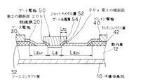
図11は、従来のFPFETの一構成例を示す断面構造図である。図11に示すように、ゲート電極150に備えたFPの長さであるLfpを1.0μmと長くすることで、絶縁膜120下の動作層12に発生する電界集中が緩和され、耐圧が向上する。一方、FPが半導体表面の一部を覆うため、FPにて表面空乏層を制御することが出来、パルス分散の発生が抑制される。このように、FPを備えることで、高耐圧を得つつ、パルス分散を抑制することが可能となる。
【0005】
【特許文献1】
特開2000−100831号公報
【0006】
【発明が解決しようとする課題】
しかし、上述のFPFETは、FP長が長いため、絶縁膜をFPおよび動作層で挟んで形成されてしまう容量(寄生容量)が増加することで、利得が低下するという問題があった。寄生容量を減らすためにFPを短くすると、FPによる電界緩和の効果が急激に消滅してしまう。このことから、FPによる電界緩和と利得はトレードオフにあり、利得の要求が厳しいデバイスではFPの適用は困難であった。
【0007】
本発明は上記したような従来の技術が有する問題点を解決するためになされたものであり、電界緩和効果を得るとともに、利得を向上させた電界効果型トランジスタおよびその製造方法を提供することを目的とする。
【0008】
【課題を解決するための手段】
上記目的を達成するための本発明の電界効果型トランジスタは、半導体動作層上に形成されたソース電極およびドレイン電極と、
前記半導体動作層上の前記ソース電極と前記ドレイン電極間に形成される、前記ドレイン電極側の側壁が前記半導体動作層上面と垂直な面から前記ドレイン電極側に傾いて形成された第1の傾斜部を備えた開口を有する絶縁膜と、
前記開口を介して前記半導体動作層と接合された、少なくとも前記ドレイン電極側の側壁を覆うゲート電極と、
を有する構成である。
【0009】
本発明では、ゲート電極が第1の傾斜部を覆っているため、ゲート電極への電圧印加時における開口端に集中する電界がドレイン電極側に分散し、半導体動作層内に生じる電界集中が緩和される。
【0010】
また、上記本発明の電界効果型トランジスタにおいて、前記半導体動作層上面に対して前記第1の傾斜部の角度が30〜60度であることとしてもよい。
【0011】
本発明では、半導体動作層上面に対して第1の傾斜部の角度が30度より大きければ、絶縁膜をゲート電極と半導体動作層で挟んで形成されてしまう容量(寄生容量)が大きくなることで発生する、利得の低下をより抑制できる。また、半導体動作層上面に対して第1の傾斜部の角度が60度より小さければ、ゲート電極への電圧印加時における開口端に集中する電界がよりドレイン電極側に分散し、半導体動作層内に生じる電界集中が十分に緩和される。
【0012】
また、上記本発明の電界効果型トランジスタにおいて、前記開口は、前記ソース電極側の側壁が前記半導体動作層上面と垂直な面から前記ソース電極側に傾いて形成された第2の傾斜部を備え、
前記ゲート電極の前記ソース電極側の側壁が前記第2の傾斜部上に形成されたこととしてもよい。
【0013】
本発明では、ゲート電極のソース電極側の側壁が第2の傾斜部上にあるため、ソース電極側のゲート電極の寄生容量が低減される。そのため、利得がより向上する。
【0014】
さらに、上記本発明の電界効果型トランジスタにおいて、前記開口から前記ソース電極側に形成された前記絶縁膜の一部が前記ゲート電極で覆われ、
前記絶縁膜の一部における最大膜厚が、前記第1の傾斜部の上端から前記ドレイン電極側の前記絶縁膜の膜厚に比べて厚いこととしてもよい。
【0015】
本発明では、開口からソース電極側の絶縁膜の一部における最大膜厚が第1の傾斜部上端からドレイン電極側の絶縁膜の膜厚より厚いため、ソース電極側の寄生容量が低減される。そのため、利得がさらに向上する。
【0016】
一方、上記目的を達成するための本発明の電界効果型トランジスタの製造方法は、半導体動作層上のソース電極およびドレイン電極間にゲート電極を有する電界効果型トランジスタの製造方法であって、
前記半導体動作層上の前記ソース電極と前記ドレイン電極間に形成された絶縁膜に、前記ドレイン電極側の側壁が前記半導体動作層上面と垂直な面から前記ドレイン電極側に傾いて形成された傾斜部を備える、前記半導体動作層の一部を露出させるための開口を形成し、
少なくとも前記傾斜部と前記開口の前記半導体動作層上面を覆う前記ゲート電極を形成するものである。
【0017】
本発明では、半導体動作層上の絶縁膜に、ドレイン電極側の側壁が半導体動作層上面と垂直な面からドレイン電極側に傾いて形成された傾斜部を備える開口を形成し、この傾斜部を覆うようにゲート電極を形成しているため、ゲート電極への電圧印加時における開口端に集中する電界がドレイン電極側に分散し、半導体動作層内に生じる電界集中が緩和される。
【0018】
また、上記本発明の電界効果型トランジスタの製造方法において、前記絶縁膜は、
前記傾斜部上端から前記ドレイン電極側の部位よりも前記開口の前記ソース電極側の端から前記ソース電極側の部位の膜厚が厚いこととしてもよい。
【0019】
本発明では、絶縁膜のうち、開口の傾斜部上端からドレイン電極側の部位よりも開口のソース電極側の端からソース電極側の部位の膜厚が厚いため、ゲート電極形成の際、半導体動作層が損傷を受けるのを十分に防止できる。
【0020】
また、上記本発明の電界効果型トランジスタの製造方法において、前記開口を形成するためのフォトレジストを前記絶縁膜上に形成し、
前記絶縁膜よりも前記フォトレジストのエッチング速度が大きい条件で、かつ前記半導体動作層上面に対して前記傾斜部の角度が60度よりも小さくなるように前記絶縁膜をエッチングすることで、前記開口を形成することとしてもよい。
【0021】
本発明では、開口形成の際、絶縁膜よりもフォトレジストのエッチング速度が大きいため、半導体動作層上面に対して傾斜部の角度が45度より大きく形成され、また、その角度が60度を越えないようにすることで、ゲート電極への電圧印加時における開口端に集中する電界がよりドレイン電極側に分散し、半導体動作層内に生じる電界集中が十分に緩和される。
【0022】
また、上記本発明の電界効果型トランジスタの製造方法において、前記開口を形成するためのフォトレジストを前記絶縁膜上に形成し、
前記絶縁膜よりも前記フォトレジストのエッチング速度が小さい条件で、かつ前記半導体動作層上面に対して前記傾斜部の角度が30度よりも大きくなるように前記絶縁膜をエッチングすることで、前記開口を形成することとしてもよい。
【0023】
本発明では、開口形成の際、絶縁膜よりもフォトレジストのエッチング速度が小さいため、半導体動作層上面に対して傾斜部の角度が45度よりも小さく形成され、また、その角度が30度よりも大きくなるようにすることで、ゲート電極による寄生容量の増加を防ぎ、利得の低下をより抑制できる。
【0024】
さらに、上記本発明の電界効果型トランジスタの製造方法において、前記開口を形成するためのフォトレジストを前記絶縁膜上に形成し、
前記絶縁膜と前記フォトレジストのエッチング速度が等しい条件で前記絶縁膜をエッチングすることで、前記開口を形成することとしてもよい。
【0025】
本発明では、開口形成の際、絶縁膜とフォトレジストのエッチング速度が等しいため、半導体動作層上面に対してドレイン電極側傾斜部の角度が45度に形成される。そのため、ゲート電極への電圧印加時における開口端に集中する電界がドレイン電極側に分散し、半導体動作層内に生じる電界集中が十分に緩和される。また、ゲート電極による寄生容量の増加を防ぎ、利得の低下を抑制できる。
【0026】
【発明の実施の形態】
本発明の電界効果型トランジスタは、ゲート電極が動作層に接合される開口を有する絶縁膜に、ドレイン電極側の側壁が動作層上面と垂直な面からドレイン電極側に傾いて形成された傾斜部を設けたことを特徴とする。
【0027】
(第1実施例)
本実施例の電界効果型トランジスタ(以下、FETと称する)について説明する。
【0028】
図1は本実施例のFETの一構成例を示す断面構造図である。
【0029】
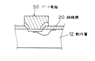
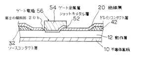
図1に示すように、本実施例のFETは、ソース電極30およびドレイン電極40間の半導体基板10上に形成された動作層12表面における幅広の窪み部であるワイドリセス部に、動作層12上の絶縁膜20に形成された開口を介して動作層12にショットキ接合したゲート電極50が形成されている。絶縁膜20の開口は、ドレイン電極40側の側壁が動作層12上面と垂直な面からドレイン電極40側に傾いて形成された第1の傾斜部20aと、ソース電極30側の側壁が動作層12上面と垂直な面からソース電極30側に傾いて形成された第2の傾斜部20bとを有する構成である。本実施例では、第1の傾斜部20aおよび第2の傾斜部20bはゲート電極50に覆われている。
【0030】
ゲート電極50は、第1の傾斜部20a、第2の傾斜部20b、および開口の動作層12に接触するショットキメタル層52と、ショットキメタル層52上に形成されたゲート金属層54とを有する構成である。ゲート電極50のうち、動作層12に接触しない部位のドレイン電極40側がFP部となる。なお、本実施例のFETは、上述したように、ゲート電極50にFP部を含む構成であるため、一体型FPFETと称する。
【0031】
図1に示す絶縁膜20の膜厚は、第1の傾斜部20aおよび第2の傾斜部20bを除いた領域では200nmであり、第1の傾斜部20aおよび第2の傾斜部20bではショットキ接合部に近づくにつれて薄くなっている。
【0032】
動作層12上面に対する第1の傾斜部20aの角度、および動作層12上面に対する第2の傾斜部20bの角度である傾斜部角度は、45度に形成されている。この角度は30度から60度の範囲であることが望ましい。傾斜部角度が30度より小さい場合には、傾斜部の長さが長くなり、傾斜部上に形成されるゲート電極50の面積が増えることで寄生容量が増加し、利得が低下する。傾斜部角度が60度より大きい場合には、FPの電界緩和効果が低下するため、FP長を長くする必要が生じ、角度が30度より小さい場合と同様に、寄生容量が増加し、利得が低下することになる。
【0033】
また、図1に示すように、ショットキ接合部端からドレイン電極40側のゲート電極50の長さLfpは0.5μmに形成されている。ショットキ接合部端からソース電極30側ゲート電極50の長さが0.5μmに形成されている。ワイドリセス部の長さのうち、ゲート電極50と動作層12とのショットキ接合部の長さであるゲート長Lgを除いたソース電極30側の長さをLgsrとし、ドレイン電極40側の長さをLgdrとすると、Lgsr=1.0μm、Lgdr=2.5μmに形成されている。
【0034】
なお、Lfp、Lgsr、およびLgdrの寸法は、上記値に限定されない。また、以下では、ゲート電極50と動作層12とのショットキ接合部において、Lgと直交する方向の寸法をゲート幅と称する。
【0035】
次に、上述した構成のFETの製造方法について説明する。なお、ソース電極30およびドレイン電極40の形成、ならびに配線形成等の工程は、従来のFET製造方法と同様なため、その詳細な説明を省略する。
【0036】
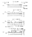
図2は本実施例のFETの製造方法を示す断面構造図である。
【0037】
図2(a)に示すように、半導体基板10上にGaAs半導体の動作層12を成膜し、動作層12の上にn+GaAs半導体のコンタクト層を形成する。コンタクト層にワイドリセス部を形成してソースコンタクト層32およびドレインコンタクト層42を形成する。その後、ソースコンタクト層32、ドレインコンタクト層42、および動作層12上に、絶縁膜として酸化膜(SiO2膜)22を形成する。
【0038】
続いて、周知のフォトリソグラフィ工程(以下、「フォトリソ工程」と称する)により、SiO2膜22の上に、ゲート電極50を動作層12に接合するための開口以外のSiO2膜22を覆うためのフォトレジスト(PR)であるゲート開口PR62を形成する(図2(b))。なお、このゲート開口PR62が、この後のエッチング工程におけるサイドエッチングにより広がることを考慮して、予めマスクパターンの開口を細めに設計したり、露光量を調節したりする必要がある。
【0039】
その後、ECR(Electron Cyclotron Resonance)プラズマエッチング装置を用いて、エッチングガスSF6、圧力0.5〜0.9mTorr、マイクロ波パワー100〜150W、RFパワー5〜10Wの条件でSiO2膜22をドライエッチングして開口を形成する。このドライエッチングにより、SiO2膜22およびゲート開口PR62がサイドエッチングされるため、SiO2膜22のエッチングが進むにつれてゲート開口PR62の開口幅が広がり、SiO2膜22開口に断面エッチング形状が斜めの第1の傾斜部22aおよび第2の傾斜部22bが形成される(図2(c))。第1の傾斜部22aおよび第2の傾斜部22bの傾斜部角度は、ゲート開口PR62のサイドエッチング速度、およびSiO2膜22のエッチング速度で決定される。ここでは、これらのエッチング速度を同じにしたため、傾斜部角度は45度になった。
【0040】
なお、ゲート開口PR62に用いられるPRの種類、ならびにドライエッチング処理におけるガスの種類、圧力、および温度等の処理条件を最適化し、ゲート開口PR62とSiO2膜22の選択エッチング特性を変えることにより、傾斜部角度を任意の値に形成できる。ゲート開口PR62のサイドエッチング速度とSiO2膜22のエッチング速度とを比較して、ゲート開口PR62の方が大きければ、傾斜部角度は45度よりも大きくなる。反対に、SiO2膜22のエッチング速度の方が大きければ、傾斜部角度は45度よりも小さくなる。
【0041】
続いて、ゲート開口PR62を除去した後、ショットキメタル層52としてタングステンシリサイド(WSi)を形成し、その上にゲート金属層54として金(Au)を形成する。そして、フォトリソ工程により、FPを含むゲート電極部を覆うゲート加工PR64を形成した後、イオンミリング処理によりゲート電極50を形成する(図2(d))。なお、FP部は、図2(d)に示すように、傾斜部22bを覆い、SiO2膜22の平坦部に達する長さに形成している。
【0042】
その後、従来と同様に、ソースコンタクト層32およびドレインコンタクト層42上のSiO2膜22に開口を設け、AuGeNi金属によるソース電極30およびドレイン電極40を形成する。
【0043】
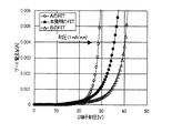
次に、ゲート電極とドレイン電極間の2端子耐圧特性評価に用いた実験サンプルついて説明する。
【0044】
図3は、従来技術によるFETの一構成例を示す断面構造図である。図4は、上述した構成の本実施例の断面構造図である。なお、図3および図4は、ゲート電極形状、および電界強度の様子を説明するための模式図であり、ソース電極およびドレイン電極等の構成を示すことを省略している。
【0045】
図3に示す実験サンプルAは、図10に示した従来のFET(以下、「実験サンプルB」とする)に比べてFP長の短いゲート電極を有する構成である。図3および図10に示すように、実験サンプルAおよびBは、ゲート電極150、152と絶縁膜120の接触面が動作層12上面に対してほぼ垂直になっている。
【0046】
次に、2端子耐圧特性評価の結果について説明する。
【0047】
図5は、上記3つの実験サンプルについて、2端子耐圧特性を比較した結果を示すグラフである。横軸はゲート電極に印加する電圧値を示し、縦軸はゲート電極とドレイン電極間に流れるゲート電流Igを示す。耐圧値は、ゲート幅の単位長さあたりの電流値で規定し、Igが1mA/mmになるときの電圧値とした。
【0048】
図5に示すグラフから、耐圧値は、実験サンプルAのFETが28V程度であるのに対して、本実施例のFETは36Vであり、実験サンプルBのFETは40V程度であった。本実施例のFETにおいても、FPの特徴である耐圧向上効果が認められた。これは、図4に示すように、ゲート電極と絶縁膜との接触面に傾斜部を設けることで、ゲート電極下での電界が緩和されたためと考えられる。
【0049】
図3および図4に、電界強度を模式的に示す。図3に示すように、実験サンプルAでは、ショットキ接合部のドレイン電極側端で電界が異常に大きくなって、電界強度の緩和が不十分であると考えられる。これに対して、図4に示すように、本実施例では、電界強度がドレイン電極側に分散し、電界強度の極大部が、図3に比べて小さくなっており、電界強度が十分に緩和されていると考えられる。
【0050】
次に、上記3つの実験サンプルのRF特性について説明する。
【0051】
図6は、上記3つの実験サンプルについて、RF特性を比較した結果を示すグラフである。横軸は入力電力を示し、縦軸は出力電力を示す。評価には、ゲート幅4mmのFETにて、動作電圧18V、周波数1.5GHzで行った。FETの特性を十分に引き出すために、入力側は利得整合、出力側はパワー整合とした。
【0052】
図6に示すように、入力電力が20dBmより大きくなると、実験サンプルAの出力電力の値が飽和する。これに対して、本実施例および実験サンプルBのグラフの傾きは緩くなるが出力電力が増加し、実験サンプルAに比べて、出力電力が1dB向上していることがわかる。これは、実験サンプルAに対して、実験サンプルBおよび本実施例のFETは、パルス分散の発生が抑制されたためと考えられる。
【0053】
一方、図6に示すように、入力電力に対して出力電力が線形に変化する領域のうち、入力電力10dBmにおける出力電力を比較すると、本実施例が実験サンプルBに比べて、利得が2dB向上していることがわかる。FP長を短くしたことによって寄生容量が低減し、利得が向上した。
【0054】
上述の結果から、本実施例のFETは、動作層上の絶縁膜に、ドレイン電極側の側壁が動作層上面と垂直な面からドレイン電極側に傾いて形成された傾斜部を備える開口が形成され、この傾斜部を覆うようにゲート電極が形成されている。そのため、ゲート電極への電圧印加時における開口端に集中する電界がドレイン電極側に分散し、動作層内に生じる電界集中が緩和される。また、FP部を短くしたことにより寄生容量が低減し、十分な利得を得ることができる。
【0055】
なお、絶縁膜としてSiO2膜22をエッチングする際、エッチングに用いられるガスは、上記SF6の代わりに、CF4および酸素(O2)を含む混合ガスであってもよい。CF4ガスは主にSiO2膜22をエッチングし、O2ガスは主にゲート開口PR62をエッチングするので、この二つのガスの混合比を調節することで、傾斜部角度を任意の角度に形成できる。
【0056】
(第2実施例)
本実施例のFETは、第1実施例のゲート電極のソース電極側部分を短くしたことを特徴とする。
【0057】
本実施例のFETの構成について説明する。
【0058】
図7は本実施例のFETの構成を示す断面構造図である。図7に示すように、本実施例のFETは、第1実施例で示したゲート電極のソース電極側部分が短く、ゲート電極56のソース電極側の側壁が第2の傾斜部20b上に形成されている。
【0059】
本実施例のFETのゲート電極56は、第1実施例で示した図2(d)において、ゲート加工PR64形成のためのマスク寸法を調整し、ソース電極側の傾斜部上のショットキメタル層52およびゲート金属層54をイオンミリングにて除去することで形成される。
【0060】
本実施例では、ゲート電極のソース電極側部分を短くしたことにより、ソース電極側の不要な寄生容量をなくし、利得を上げることが可能である。
【0061】
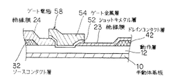
(第3実施例)
本実施例のFETは、ゲート電極に覆われる絶縁膜のうち、ソース電極側をドレイン電極側に比べて膜厚を厚くしたことを特徴とする。
【0062】
本実施例のFETの構成について説明する。
【0063】
図8は本実施例のFETの構成を示す断面構造図である。図8に示すように、本実施例のFETは、ショットキ接合部端からソース電極側の絶縁膜24がドレイン電極側の絶縁膜23に比べて膜厚が厚く、ソース電極側の傾斜部角度がより垂直に近い構成である。
【0064】
本実施例のFETの製造方法について説明する。なお、第1実施例と同様の工程については、その詳細な説明を省略する。
【0065】
図9は本実施例のFETの製造方法を示す断面構造図である。
【0066】
上述の第1実施例と同様にして、ソースコンタクト層32およびドレインコンタクト層42を形成した後、絶縁膜としてSiO2膜25を200nm形成する。続いて、フォトリソ工程により、ショットキ接合部のソース電極側の端からソース電極形成部側を覆う片側PR66を形成し、図9(a)に示すように、上記ショットキ接合部および接合部のソース電極側の端からドレイン電極形成部側のSiO2膜25をウェットエッチングにより除去する。そして、片側PR66を除去した後、絶縁膜としてSiO2膜26を200nm形成し、第1実施例と同様に、ゲート開口PR62を形成する(図9(b))。その後、第1実施例と同様の条件で、ドライエッチングにてSiO2膜26をエッチングする(図9(c))。その後、ゲート開口PR62を除去し、第1実施例と同様に処理を行う。
【0067】
図9(c)に示したように、SiO2膜の膜厚が、ドレイン電極側ではSiO2膜26の200nmであるのに対して、ソース電極側ではSiO2膜25およびSiO2膜26の400nmと厚くなるので、SiO2膜25およびSiO2膜26を有する絶縁膜24の傾斜部角度はソース電極側がより垂直に近くなる。
【0068】
本実施例では、ショットキ接合部端からソース電極側の絶縁膜の膜厚が従来に比べて厚いため、マスクとの合わせずれで、ゲート加工PR64がドレイン電極側にずれても、ゲート加工の際、イオンミリングにより動作層12が損傷することを防げる。
【0069】
また、ソース電極側のゲート電極の長さが長くても、絶縁膜の膜厚を従来よりも厚くしているため寄生容量を低減できる。
【0070】
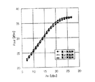
上述した第1実施例〜第3実施例のFETについて、RF入出力特性のグラフを図10に示す。グラフの横軸は入力電力を示し、縦軸は出力電力を示す。
【0071】
図10に示すように、第2実施例および第3実施例のFETは、第1実施例のFETよりも0.5dB程度利得が向上している。
【0072】
なお、第1実施例〜第3実施例において、絶縁膜20、23、24は、上記SiO2膜に限らず、SiN膜などの他の絶縁膜であってもよい。絶縁膜20、23の成膜膜厚は、上述の場合の200nmに限らないが、FPの効果を高めるために、300nm以下であることが望ましい。
【0073】
【発明の効果】
本発明は以上説明したように構成されているので、以下に記載する効果を奏する。
【0074】
本発明では、動作層上の絶縁膜に、ドレイン電極側の側壁が動作層上面と垂直な面からドレイン電極側に傾いて形成された傾斜部を備える開口が形成され、この傾斜部を覆うようにゲート電極が形成されている。そのため、ゲート電極への電圧印加時における開口端に集中する電界がドレイン電極側に分散し、FPによる電界緩和効果が保持される。
【0075】
また、ゲート電極のソース電極側の側壁が絶縁膜の傾斜部上に形成されるようにすることで、ソース電極側のゲート電極の寄生容量が低減され、利得がより向上する。
【0076】
さらに、動作層上に形成された絶縁膜のうち、ドレイン電極側の傾斜部上端からドレイン電極側の部位よりも開口のソース電極側の端からソース電極側の部位の膜厚を厚くすることで、ソース電極側の寄生容量が低減され、利得がさらに向上する。
【図面の簡単な説明】
【図1】第1実施例のFETの一構成例を示す断面構造図である。
【図2】第1実施例のFETの製造方法の一例を示す断面構造図である。
【図3】FPを有していない、従来のFETの断面構造図、および電界の強さを示す模式図である。
【図4】第1実施例のFETの断面構造図、および電界の強さを示す模式図である。
【図5】従来技術と第1実施例のFETについて、耐圧特性を比較した結果を示すグラフである。
【図6】従来技術と第1実施例のFETについて、RF特性を比較した結果を示すグラフである。
【図7】第2実施例のFETの断面構造図である。
【図8】第3実施例のFETの断面構造図である。
【図9】第3実施例のFETの製造方法を示す断面構造図である。
【図10】第1実施例〜第3実施例のFETの入出力特性を示すグラフである。
【図11】従来のFPFETの一構成例を示す断面構造図である。
【符号の説明】
10 半導体基板
12 動作層
20、23、24、120 絶縁膜
20a、22a 第1の傾斜部
20b、22b 第2の傾斜部
22、25、26 SiO2膜
30 ソース電極
32 ソースコンタクト層
40 ドレイン電極
42 ドレインコンタクト層
50、56、58、150、152 ゲート電極
52 ショットキメタル層
54 ゲート金属層
62 ゲート開口PR
64 ゲート加工PR
66 片側PR[0001]
TECHNICAL FIELD OF THE INVENTION
The present invention relates to a field-effect transistor that controls a current flowing between a source electrode and a drain electrode by a voltage applied to a gate electrode, and a method for manufacturing the same.
[0002]
[Prior art]
2. Description of the Related Art Conventionally, among field effect transistors (FETs), MES (Metal Semiconductor) FETs in which a gate electrode is joined to a semiconductor operation layer (hereinafter, simply referred to as an operation layer) that generates a depletion layer and a channel, The current flowing between the source electrode and the drain electrode is controlled by changing the spread of the depletion layer in the operation layer according to the voltage applied to the gate electrode. Among MESFETs, in particular, an FET using a compound semiconductor such as GaAs as an active layer has an electron mobility several times larger than that of a silicon semiconductor and is often used as a high-frequency FET.
[0003]
In the high-frequency FET described above, the surface depletion layer spreads on the semiconductor surface between the gate electrode and the drain electrode, so that pulse dispersion occurs in which the gate cannot control the depletion layer for high-frequency signals, and the output decreases and This may cause problems such as deterioration of distortion. On the other hand, when increasing the output of a high-frequency FET, high-voltage operation is effective, but high-voltage operation requires a high withstand voltage of the FET. In order to obtain a high withstand voltage, it is necessary to increase the distance between the gate electrode and the drain electrode.However, the surface depletion layer is easily affected by roughness and contamination of the semiconductor surface. In this case, the output is not generated according to the voltage, and the efficiency is reduced. In order to improve this, an FPFET, which is an FET provided with an FP (Field-Modulated Plate) as a gate electrode, has been proposed (for example, see Patent Document 1).
[0004]
FIG. 11 is a cross-sectional structure diagram showing a configuration example of a conventional FPFET. As shown in FIG. 11, by increasing Lfp, which is the length of the FP provided in the gate electrode 150, to 1.0 μm, the electric field concentration generated in the
[0005]
[Patent Document 1]
JP-A-2000-100831
[0006]
[Problems to be solved by the invention]
However, since the FPFET has a long FP length, there is a problem in that the capacitance (parasitic capacitance) formed by sandwiching the insulating film between the FP and the operation layer increases, and the gain decreases. If the FP is shortened in order to reduce the parasitic capacitance, the effect of the FP to alleviate the electric field rapidly disappears. For this reason, there is a trade-off between the electric field relaxation and the gain by the FP, and it has been difficult to apply the FP to a device requiring a strict gain.
[0007]
The present invention has been made in order to solve the problems of the conventional technology as described above, and an object of the present invention is to provide a field-effect transistor having an improved electric field relaxation effect and an improved gain, and a method of manufacturing the same. Aim.
[0008]
[Means for Solving the Problems]
The field effect transistor of the present invention for achieving the above object, a source electrode and a drain electrode formed on a semiconductor operation layer,
A first slope formed between the source electrode and the drain electrode on the semiconductor operation layer, wherein a side wall on the drain electrode side is inclined from a plane perpendicular to an upper surface of the semiconductor operation layer toward the drain electrode; An insulating film having an opening with a portion,
A gate electrode joined to the semiconductor operation layer through the opening, and covering at least a side wall on the drain electrode side;
It is a structure which has.
[0009]
In the present invention, since the gate electrode covers the first inclined portion, the electric field concentrated on the opening end when a voltage is applied to the gate electrode is dispersed on the drain electrode side, and the electric field concentration generated in the semiconductor operation layer is reduced. Is done.
[0010]
In the field effect transistor according to the present invention, the angle of the first inclined portion with respect to the upper surface of the semiconductor operation layer may be 30 to 60 degrees.
[0011]
In the present invention, if the angle of the first inclined portion with respect to the upper surface of the semiconductor operation layer is larger than 30 degrees, the capacitance (parasitic capacitance) formed by sandwiching the insulating film between the gate electrode and the semiconductor operation layer is increased. , And a decrease in the gain that occurs in the above can be further suppressed. Further, if the angle of the first inclined portion with respect to the upper surface of the semiconductor operation layer is smaller than 60 degrees, the electric field concentrated on the opening end when voltage is applied to the gate electrode is more dispersed on the drain electrode side, and Is sufficiently reduced.
[0012]
Further, in the field effect transistor according to the present invention, the opening includes a second inclined portion in which a side wall on the source electrode side is inclined from a plane perpendicular to an upper surface of the semiconductor operation layer toward the source electrode. ,
A side wall of the gate electrode on the source electrode side may be formed on the second inclined portion.
[0013]
In the present invention, since the side wall of the gate electrode on the source electrode side is on the second inclined portion, the parasitic capacitance of the gate electrode on the source electrode side is reduced. Therefore, the gain is further improved.
[0014]
Further, in the field-effect transistor of the present invention, a part of the insulating film formed on the source electrode side from the opening is covered with the gate electrode,
A maximum thickness of a part of the insulating film may be larger than a thickness of the insulating film on the drain electrode side from an upper end of the first inclined portion.
[0015]
In the present invention, since the maximum thickness of a part of the insulating film on the source electrode side from the opening is larger than the thickness of the insulating film on the drain electrode side from the upper end of the first inclined portion, the parasitic capacitance on the source electrode side is reduced. . Therefore, the gain is further improved.
[0016]
On the other hand, a method for manufacturing a field-effect transistor of the present invention for achieving the above object is a method for manufacturing a field-effect transistor having a gate electrode between a source electrode and a drain electrode on a semiconductor operation layer,
In the insulating film formed between the source electrode and the drain electrode on the semiconductor operation layer, a slope formed such that a sidewall on the drain electrode side is inclined from a plane perpendicular to the upper surface of the semiconductor operation layer toward the drain electrode. Forming an opening for exposing a part of the semiconductor operation layer,
Forming the gate electrode covering at least the inclined portion and the upper surface of the semiconductor operation layer in the opening;
[0017]
In the present invention, in the insulating film on the semiconductor operation layer, an opening having a slope formed by inclining the side wall on the drain electrode side from the surface perpendicular to the upper surface of the semiconductor operation layer toward the drain electrode side is formed, and this slope is formed. Since the gate electrode is formed so as to cover, the electric field concentrated at the opening end when a voltage is applied to the gate electrode is dispersed toward the drain electrode, and the electric field concentration generated in the semiconductor operation layer is reduced.
[0018]
In the method for manufacturing a field-effect transistor according to the present invention, the insulating film may include:
The thickness of a portion of the opening closer to the source electrode than the end of the opening closer to the source electrode may be thicker than a portion of the opening closer to the drain electrode than a portion closer to the drain electrode.
[0019]
In the present invention, the thickness of the insulating film is larger at the portion from the upper end of the opening to the drain electrode than at the portion from the upper end of the opening to the drain electrode, so that when the gate electrode is formed, The layer can be sufficiently prevented from being damaged.
[0020]
In the method of manufacturing a field-effect transistor according to the present invention, a photoresist for forming the opening is formed on the insulating film;
The opening is formed by etching the insulating film under the condition that the etching rate of the photoresist is higher than that of the insulating film and the angle of the inclined portion with respect to the upper surface of the semiconductor operation layer is smaller than 60 degrees. May be formed.
[0021]
In the present invention, since the etching rate of the photoresist is higher than that of the insulating film when forming the opening, the angle of the inclined portion is formed larger than 45 degrees with respect to the upper surface of the semiconductor operation layer, and the angle exceeds 60 degrees. By avoiding this, the electric field concentrated on the opening end when a voltage is applied to the gate electrode is more dispersed on the drain electrode side, and the electric field concentration generated in the semiconductor operation layer is sufficiently reduced.
[0022]
In the method of manufacturing a field-effect transistor according to the present invention, a photoresist for forming the opening is formed on the insulating film;
By etching the insulating film under the condition that the etching rate of the photoresist is lower than that of the insulating film and the angle of the inclined portion with respect to the upper surface of the semiconductor operation layer is larger than 30 degrees, the opening is formed. May be formed.
[0023]
In the present invention, since the etching rate of the photoresist is lower than that of the insulating film when forming the opening, the angle of the inclined portion with respect to the upper surface of the semiconductor operation layer is formed smaller than 45 degrees, and the angle is set smaller than 30 degrees. Is increased, the increase in the parasitic capacitance due to the gate electrode can be prevented, and the decrease in gain can be further suppressed.
[0024]
Further, in the method for manufacturing a field-effect transistor according to the present invention, a photoresist for forming the opening is formed on the insulating film;
The opening may be formed by etching the insulating film under the condition that the etching rates of the insulating film and the photoresist are equal.
[0025]
In the present invention, since the etching rate of the insulating film and that of the photoresist are equal when forming the opening, the angle of the inclined portion on the drain electrode side with respect to the upper surface of the semiconductor operation layer is formed at 45 degrees. Therefore, the electric field concentrated on the opening end when a voltage is applied to the gate electrode is dispersed on the drain electrode side, and the electric field concentration generated in the semiconductor operation layer is sufficiently reduced. In addition, an increase in parasitic capacitance due to the gate electrode can be prevented, and a decrease in gain can be suppressed.
[0026]
BEST MODE FOR CARRYING OUT THE INVENTION
The field-effect transistor according to the present invention has an inclined portion in which an insulating film having an opening in which a gate electrode is joined to an operation layer has a side wall on the drain electrode side inclined from a plane perpendicular to the upper surface of the operation layer toward the drain electrode side. Is provided.
[0027]
(First embodiment)
A field effect transistor (hereinafter referred to as an FET) of the present embodiment will be described.
[0028]
FIG. 1 is a cross-sectional structure diagram showing one configuration example of the FET of this embodiment.
[0029]
As shown in FIG. 1, the FET of the present embodiment has a wide recess portion, which is a wide recess on the surface of the
[0030]
The
[0031]
The thickness of the insulating
[0032]
The angle of the first inclined portion 20a with respect to the upper surface of the
[0033]
Further, as shown in FIG. 1, the length Lfp of the
[0034]
The dimensions of Lfp, Lgsr, and Lgdr are not limited to the above values. In the following, a dimension in a direction orthogonal to Lg at a Schottky junction between
[0035]
Next, a method of manufacturing the FET having the above configuration will be described. Since the steps of forming the
[0036]
FIG. 2 is a sectional structural view showing the method for manufacturing the FET of this embodiment.
[0037]
As shown in FIG. 2A, an
[0038]
Subsequently, by a known photolithography process (hereinafter, referred to as “photolithography process”), SiO 2 is formed. 2 On the
[0039]
Thereafter, using an ECR (Electron Cyclotron Resonance) plasma etching apparatus, the etching gas SF is used. 6 At a pressure of 0.5 to 0.9 mTorr, a microwave power of 100 to 150 W, and an RF power of 5 to 10 W. 2 An opening is formed by dry etching the
[0040]
The type of PR used for the gate opening PR62 and the processing conditions such as the type, pressure, and temperature of the gas in the dry etching process are optimized, and the gate opening PR62 and the SiO 2 By changing the selective etching characteristics of the
[0041]
Subsequently, after removing the gate opening PR62, tungsten silicide (WSi) is formed as the
[0042]
Thereafter, as in the conventional case, the SiO 2 on the
[0043]
Next, an experimental sample used for evaluating the two-terminal breakdown voltage characteristics between the gate electrode and the drain electrode will be described.
[0044]
FIG. 3 is a cross-sectional structure diagram showing one configuration example of a conventional FET. FIG. 4 is a sectional structural view of the present embodiment having the above-described configuration. FIGS. 3 and 4 are schematic diagrams for explaining the shape of the gate electrode and the state of the electric field intensity, and omit the configuration of the source electrode, the drain electrode, and the like.
[0045]
The experimental sample A shown in FIG. 3 has a configuration having a gate electrode with a shorter FP length than the conventional FET shown in FIG. 10 (hereinafter referred to as “experimental sample B”). As shown in FIGS. 3 and 10, in the experimental samples A and B, the contact surfaces between the gate electrodes 150 and 152 and the insulating film 120 are substantially perpendicular to the upper surface of the
[0046]
Next, the results of the two-terminal breakdown voltage characteristic evaluation will be described.
[0047]
FIG. 5 is a graph showing the results of comparing the two-terminal breakdown voltage characteristics of the three experimental samples. The horizontal axis indicates the voltage value applied to the gate electrode, and the vertical axis indicates the gate current Ig flowing between the gate electrode and the drain electrode. The withstand voltage value was defined by a current value per unit length of the gate width, and was defined as a voltage value when Ig became 1 mA / mm.
[0048]
From the graph shown in FIG. 5, the withstand voltage value was about 28 V for the FET of the experimental sample A, 36 V for the FET of the present example, and about 40 V for the FET of the experimental sample B. Also in the FET of this example, the effect of improving the breakdown voltage, which is a feature of the FP, was recognized. This is probably because the electric field under the gate electrode was reduced by providing an inclined portion on the contact surface between the gate electrode and the insulating film as shown in FIG.
[0049]
3 and 4 schematically show the electric field strength. As shown in FIG. 3, in the experimental sample A, the electric field becomes abnormally large at the end of the Schottky junction on the drain electrode side, and it is considered that the relaxation of the electric field intensity is insufficient. On the other hand, as shown in FIG. 4, in this embodiment, the electric field intensity is dispersed on the drain electrode side, and the maximum portion of the electric field intensity is smaller than that in FIG. It is thought that it is.
[0050]
Next, the RF characteristics of the above three experimental samples will be described.
[0051]
FIG. 6 is a graph showing the results of comparing the RF characteristics of the three experimental samples. The horizontal axis shows the input power, and the vertical axis shows the output power. The evaluation was performed using an FET having a gate width of 4 mm at an operating voltage of 18 V and a frequency of 1.5 GHz. In order to sufficiently bring out the characteristics of the FET, gain matching was performed on the input side, and power matching was performed on the output side.
[0052]
As shown in FIG. 6, when the input power becomes larger than 20 dBm, the value of the output power of the experimental sample A saturates. On the other hand, although the slopes of the graphs of the present embodiment and the experimental sample B become gentler, the output power increases, and the output power is improved by 1 dB as compared with the experimental sample A. This is considered to be because the occurrence of pulse dispersion was suppressed in the experimental sample B and the FET of the present example in comparison with the experimental sample A.
[0053]
On the other hand, as shown in FIG. 6, when the output power at the input power of 10 dBm is compared in the region where the output power changes linearly with respect to the input power, the gain of the present embodiment is improved by 2 dB as compared with the experimental sample B. You can see that it is doing. By reducing the FP length, the parasitic capacitance was reduced and the gain was improved.
[0054]
From the above results, in the FET of this example, an opening was formed in the insulating film on the operation layer, having an inclined portion in which the side wall on the drain electrode side was inclined from the plane perpendicular to the upper surface of the operation layer to the drain electrode side. A gate electrode is formed so as to cover this inclined portion. Therefore, the electric field concentrated on the opening end when a voltage is applied to the gate electrode is dispersed on the drain electrode side, and the electric field concentration generated in the operation layer is reduced. Further, the parasitic capacitance is reduced by shortening the FP section, and a sufficient gain can be obtained.
[0055]
Note that SiO 2 is used as an insulating film. 2 When etching the
[0056]
(Second embodiment)
The FET of this embodiment is characterized in that the portion of the gate electrode of the first embodiment on the source electrode side is shortened.
[0057]
The configuration of the FET according to the present embodiment will be described.
[0058]
FIG. 7 is a sectional structural view showing the configuration of the FET of this embodiment. As shown in FIG. 7, in the FET of this embodiment, the portion of the gate electrode shown in the first embodiment on the source electrode side is short, and the side wall of the gate electrode 56 on the source electrode side is formed on the second inclined portion 20b. Have been.
[0059]
The gate electrode 56 of the FET of the present embodiment is obtained by adjusting the mask dimension for forming the gate processing PR 64 in FIG. 2D shown in the first embodiment, and by setting the
[0060]
In the present embodiment, by shortening the portion of the gate electrode on the source electrode side, unnecessary parasitic capacitance on the source electrode side can be eliminated, and the gain can be increased.
[0061]
(Third embodiment)
The FET of this embodiment is characterized in that the source electrode side of the insulating film covered by the gate electrode is thicker than the drain electrode side.
[0062]
The configuration of the FET according to the present embodiment will be described.
[0063]
FIG. 8 is a sectional structural view showing the configuration of the FET of this embodiment. As shown in FIG. 8, in the FET of this embodiment, the insulating film 24 on the source electrode side from the Schottky junction end is thicker than the insulating film 23 on the drain electrode side, and the angle of the inclined part on the source electrode side is small. It is a configuration that is closer to vertical.
[0064]
A method for manufacturing the FET of this embodiment will be described. The detailed description of the same steps as in the first embodiment is omitted.
[0065]
FIG. 9 is a sectional structural view showing the method for manufacturing the FET of this embodiment.
[0066]
After forming the
[0067]
As shown in FIG. 2 The thickness of the film is SiO 2 on the drain electrode side. 2 While the
[0068]
In the present embodiment, since the thickness of the insulating film on the source electrode side from the end of the Schottky junction is thicker than before, even if the gate processing PR64 is shifted to the drain electrode side due to misalignment with the mask, the gate processing is difficult. In addition, it is possible to prevent the
[0069]
Further, even if the length of the gate electrode on the source electrode side is long, the parasitic capacitance can be reduced because the thickness of the insulating film is made larger than in the conventional case.
[0070]
FIG. 10 shows a graph of the RF input / output characteristics of the FETs of the above-described first to third embodiments. The horizontal axis of the graph indicates input power, and the vertical axis indicates output power.
[0071]
As shown in FIG. 10, the gains of the FETs of the second and third embodiments are improved by about 0.5 dB as compared with the FET of the first embodiment.
[0072]
In the first to third embodiments, the insulating
[0073]
【The invention's effect】
Since the present invention is configured as described above, the following effects can be obtained.
[0074]
In the present invention, an opening having an inclined portion in which the side wall on the drain electrode side is inclined from the surface perpendicular to the upper surface of the operation layer toward the drain electrode side is formed in the insulating film on the operation layer so as to cover the inclined portion. Is formed with a gate electrode. Therefore, the electric field concentrated on the opening end when a voltage is applied to the gate electrode is dispersed on the drain electrode side, and the electric field relaxation effect by the FP is maintained.
[0075]
Further, by forming the side wall of the gate electrode on the source electrode side on the inclined portion of the insulating film, the parasitic capacitance of the gate electrode on the source electrode side is reduced, and the gain is further improved.
[0076]
Furthermore, in the insulating film formed on the operation layer, the thickness of the portion on the source electrode side from the end on the source electrode side of the opening is made thicker than the portion on the drain electrode side from the upper end of the inclined portion on the drain electrode side. In addition, the parasitic capacitance on the source electrode side is reduced, and the gain is further improved.
[Brief description of the drawings]
FIG. 1 is a cross-sectional structure diagram illustrating a configuration example of an FET according to a first embodiment.
FIG. 2 is a sectional structural view illustrating an example of a method for manufacturing the FET of the first embodiment.
FIG. 3 is a cross-sectional structure diagram of a conventional FET having no FP, and a schematic diagram showing the strength of an electric field.
FIG. 4 is a cross-sectional structure diagram of the FET of the first embodiment and a schematic diagram showing the intensity of an electric field.
FIG. 5 is a graph showing the result of comparing the withstand voltage characteristics of the FET of the prior art and the first embodiment.
FIG. 6 is a graph showing the results of comparing the RF characteristics of the FET according to the related art and the first embodiment.
FIG. 7 is a sectional structural view of an FET according to a second embodiment.
FIG. 8 is a sectional structural view of an FET according to a third embodiment.
FIG. 9 is a sectional structural view showing the method of manufacturing the FET of the third embodiment.
FIG. 10 is a graph showing input / output characteristics of the FETs of the first to third embodiments.
FIG. 11 is a cross-sectional structure diagram illustrating a configuration example of a conventional FPFET.
[Explanation of symbols]
10 Semiconductor substrate
12 Working layer
20, 23, 24, 120 insulating film
20a, 22a First inclined portion
20b, 22b Second inclined portion
22, 25, 26 SiO 2 film
30 source electrode
32 source contact layer
40 drain electrode
42 Drain contact layer
50, 56, 58, 150, 152 Gate electrode
52 Schottky metal layer
54 Gate metal layer
62 Gate opening PR
64 Gate processing PR
66 One side PR
Claims (9)
前記半導体動作層上の前記ソース電極と前記ドレイン電極間に形成される、前記ドレイン電極側の側壁が前記半導体動作層上面と垂直な面から前記ドレイン電極側に傾いて形成された第1の傾斜部を備えた開口を有する絶縁膜と、
前記開口を介して前記半導体動作層と接合された、少なくとも前記ドレイン電極側の側壁を覆うゲート電極と、
を有する電界効果型トランジスタ。A source electrode and a drain electrode formed on the semiconductor operation layer,
A first slope formed between the source electrode and the drain electrode on the semiconductor operation layer, wherein a side wall on the drain electrode side is inclined from a plane perpendicular to an upper surface of the semiconductor operation layer toward the drain electrode; An insulating film having an opening with a portion,
A gate electrode joined to the semiconductor operation layer through the opening, and covering at least a side wall on the drain electrode side;
A field-effect transistor having:
前記ゲート電極の前記ソース電極側の側壁が前記第2の傾斜部上に形成された請求項1または2記載の電界効果型トランジスタ。The opening includes a second inclined portion in which a side wall on the source electrode side is inclined from a plane perpendicular to the upper surface of the semiconductor operation layer toward the source electrode side,
3. The field effect transistor according to claim 1, wherein a side wall of the gate electrode on the side of the source electrode is formed on the second inclined portion.
前記絶縁膜の一部における最大膜厚が、前記第1の傾斜部の上端から前記ドレイン電極側の前記絶縁膜の膜厚に比べて厚い請求項1乃至3のいずれか1項記載の電界効果型トランジスタ。A part of the insulating film formed on the source electrode side from the opening is covered with the gate electrode;
4. The field effect according to claim 1, wherein a maximum thickness of a part of the insulating film is larger than a thickness of the insulating film on the drain electrode side from an upper end of the first inclined portion. 5. Type transistor.
前記半導体動作層上の前記ソース電極と前記ドレイン電極間に形成された絶縁膜に、前記ドレイン電極側の側壁が前記半導体動作層上面と垂直な面から前記ドレイン電極側に傾いて形成された傾斜部を備える、前記半導体動作層の一部を露出させるための開口を形成し、
少なくとも前記傾斜部と前記開口の前記半導体動作層上面を覆う前記ゲート電極を形成する電界効果型トランジスタの製造方法。A method for manufacturing a field-effect transistor having a gate electrode between a source electrode and a drain electrode on a semiconductor operation layer,
In the insulating film formed between the source electrode and the drain electrode on the semiconductor operation layer, a slope formed such that a sidewall on the drain electrode side is inclined from a plane perpendicular to the upper surface of the semiconductor operation layer toward the drain electrode. Forming an opening for exposing a part of the semiconductor operation layer,
A method of manufacturing a field-effect transistor, wherein the gate electrode covers at least the inclined portion and the upper surface of the semiconductor operation layer in the opening.
前記傾斜部上端から前記ドレイン電極側の部位よりも前記開口の前記ソース電極側の端から前記ソース電極側の部位の膜厚が厚い請求項5記載の電界効果型トランジスタの製造方法。The insulating film,
6. The method for manufacturing a field-effect transistor according to claim 5, wherein a film thickness of a portion on the source electrode side from the end of the opening on the source electrode side is thicker than a portion on the drain electrode side from the upper end of the inclined portion.
前記絶縁膜よりも前記フォトレジストのエッチング速度が大きい条件で、かつ前記半導体動作層上面に対して前記傾斜部の角度が60度よりも小さくなるように前記絶縁膜をエッチングすることで、前記開口を形成する請求項5または6記載の電界効果型トランジスタの製造方法。Forming a photoresist for forming the opening on the insulating film;
The opening is formed by etching the insulating film under the condition that the etching rate of the photoresist is higher than that of the insulating film and the angle of the inclined portion with respect to the upper surface of the semiconductor operation layer is smaller than 60 degrees. 7. The method for manufacturing a field-effect transistor according to claim 5, wherein
前記絶縁膜よりも前記フォトレジストのエッチング速度が小さい条件で、かつ前記半導体動作層上面に対して前記傾斜部の角度が30度よりも大きくなるように前記絶縁膜をエッチングすることで、前記開口を形成する請求項5または6記載の電界効果型トランジスタの製造方法。Forming a photoresist for forming the opening on the insulating film;
By etching the insulating film under the condition that the etching rate of the photoresist is lower than that of the insulating film and the angle of the inclined portion with respect to the upper surface of the semiconductor operation layer is larger than 30 degrees, the opening is formed. 7. The method for manufacturing a field-effect transistor according to claim 5, wherein
前記絶縁膜と前記フォトレジストのエッチング速度が等しい条件で前記絶縁膜をエッチングすることで、前記開口を形成する請求項5または6記載の電界効果型トランジスタの製造方法。Forming a photoresist for forming the opening on the insulating film;
7. The method for manufacturing a field effect transistor according to claim 5, wherein the opening is formed by etching the insulating film under the condition that the etching rates of the insulating film and the photoresist are equal.
Priority Applications (2)
| Application Number | Priority Date | Filing Date | Title |
|---|---|---|---|
| JP2003042512A JP2004253620A (en) | 2003-02-20 | 2003-02-20 | Field effect transistor and its manufacturing method |
| US10/778,199 US20040164374A1 (en) | 2003-02-20 | 2004-02-17 | Field effect transistor and method of manufacturing the same |
Applications Claiming Priority (1)
| Application Number | Priority Date | Filing Date | Title |
|---|---|---|---|
| JP2003042512A JP2004253620A (en) | 2003-02-20 | 2003-02-20 | Field effect transistor and its manufacturing method |
Publications (1)
| Publication Number | Publication Date |
|---|---|
| JP2004253620A true JP2004253620A (en) | 2004-09-09 |
Family
ID=32866436
Family Applications (1)
| Application Number | Title | Priority Date | Filing Date |
|---|---|---|---|
| JP2003042512A Pending JP2004253620A (en) | 2003-02-20 | 2003-02-20 | Field effect transistor and its manufacturing method |
Country Status (2)
| Country | Link |
|---|---|
| US (1) | US20040164374A1 (en) |
| JP (1) | JP2004253620A (en) |
Cited By (17)
| Publication number | Priority date | Publication date | Assignee | Title |
|---|---|---|---|---|
| JP2007516615A (en) * | 2003-12-17 | 2007-06-21 | ニトロネックス・コーポレーション | Gallium nitride material device including electrode defining layer and method of forming the same |
| JP2007180510A (en) * | 2005-12-01 | 2007-07-12 | Sharp Corp | Semiconductor device |
| JP2008243848A (en) * | 2007-03-23 | 2008-10-09 | Sanken Electric Co Ltd | Semiconductor device |
| JP2009004504A (en) * | 2007-06-20 | 2009-01-08 | Fujitsu Ltd | Compound semiconductor device and method of manufacturing the same |
| JP2010238838A (en) * | 2009-03-31 | 2010-10-21 | Sanken Electric Co Ltd | Semiconductor device, and method of manufacturing the same |
| JP2011114267A (en) * | 2009-11-30 | 2011-06-09 | Sanken Electric Co Ltd | Semiconductor device |
| JP2012023214A (en) * | 2010-07-14 | 2012-02-02 | Fujitsu Ltd | Compound semiconductor device and method for manufacturing the same |
| JP2012094726A (en) * | 2010-10-28 | 2012-05-17 | Fujitsu Ltd | Field-effect transistor and method of manufacturing the same |
| JP2013503483A (en) * | 2009-08-28 | 2013-01-31 | トランスフォーム インコーポレーテッド | Semiconductor device having field plate |
| JP2013058774A (en) * | 2006-01-17 | 2013-03-28 | Cree Inc | Methods of fabricating transistors including supported gate electrodes and related devices |
| US9318593B2 (en) | 2014-07-21 | 2016-04-19 | Transphorm Inc. | Forming enhancement mode III-nitride devices |
| US9536967B2 (en) | 2014-12-16 | 2017-01-03 | Transphorm Inc. | Recessed ohmic contacts in a III-N device |
| US9536966B2 (en) | 2014-12-16 | 2017-01-03 | Transphorm Inc. | Gate structures for III-N devices |
| US9590060B2 (en) | 2013-03-13 | 2017-03-07 | Transphorm Inc. | Enhancement-mode III-nitride devices |
| US10224401B2 (en) | 2016-05-31 | 2019-03-05 | Transphorm Inc. | III-nitride devices including a graded depleting layer |
| US11322599B2 (en) | 2016-01-15 | 2022-05-03 | Transphorm Technology, Inc. | Enhancement mode III-nitride devices having an Al1-xSixO gate insulator |
| US11527629B2 (en) | 2018-04-13 | 2022-12-13 | Mitsubishi Electric Corporation | Field effect transistor |
Families Citing this family (3)
| Publication number | Priority date | Publication date | Assignee | Title |
|---|---|---|---|---|
| CN102931238A (en) * | 2011-08-10 | 2013-02-13 | 美丽微半导体股份有限公司 | Constant-current semiconductor element with Schottky barrier |
| CN105118867B (en) * | 2015-08-26 | 2018-01-12 | 西安电子科技大学 | A kind of preparation method of the 4H SiC metal-semiconductor field effect transistors with part sinking raceway groove |
| DE102017127182A1 (en) * | 2017-11-17 | 2019-05-23 | Forschungsverbund Berlin E.V. | Gate structure and method for its production |
Family Cites Families (1)
| Publication number | Priority date | Publication date | Assignee | Title |
|---|---|---|---|---|
| US6159861A (en) * | 1997-08-28 | 2000-12-12 | Nec Corporation | Method of manufacturing semiconductor device |
-
2003
- 2003-02-20 JP JP2003042512A patent/JP2004253620A/en active Pending
-
2004
- 2004-02-17 US US10/778,199 patent/US20040164374A1/en not_active Abandoned
Cited By (27)
| Publication number | Priority date | Publication date | Assignee | Title |
|---|---|---|---|---|
| JP2007516615A (en) * | 2003-12-17 | 2007-06-21 | ニトロネックス・コーポレーション | Gallium nitride material device including electrode defining layer and method of forming the same |
| JP2007180510A (en) * | 2005-12-01 | 2007-07-12 | Sharp Corp | Semiconductor device |
| US7928480B2 (en) | 2005-12-01 | 2011-04-19 | Sharp Kabushiki Kaisha | Semiconductor device |
| JP4723463B2 (en) * | 2005-12-01 | 2011-07-13 | シャープ株式会社 | Semiconductor device |
| JP2013058774A (en) * | 2006-01-17 | 2013-03-28 | Cree Inc | Methods of fabricating transistors including supported gate electrodes and related devices |
| JP2008243848A (en) * | 2007-03-23 | 2008-10-09 | Sanken Electric Co Ltd | Semiconductor device |
| JP2009004504A (en) * | 2007-06-20 | 2009-01-08 | Fujitsu Ltd | Compound semiconductor device and method of manufacturing the same |
| JP2010238838A (en) * | 2009-03-31 | 2010-10-21 | Sanken Electric Co Ltd | Semiconductor device, and method of manufacturing the same |
| US9831315B2 (en) | 2009-08-28 | 2017-11-28 | Transphorm Inc. | Semiconductor devices with field plates |
| JP2013503483A (en) * | 2009-08-28 | 2013-01-31 | トランスフォーム インコーポレーテッド | Semiconductor device having field plate |
| US9111961B2 (en) | 2009-08-28 | 2015-08-18 | Transphorm Inc. | Semiconductor devices with field plates |
| US9373699B2 (en) | 2009-08-28 | 2016-06-21 | Transphorm Inc. | Semiconductor devices with field plates |
| JP2011114267A (en) * | 2009-11-30 | 2011-06-09 | Sanken Electric Co Ltd | Semiconductor device |
| JP2012023214A (en) * | 2010-07-14 | 2012-02-02 | Fujitsu Ltd | Compound semiconductor device and method for manufacturing the same |
| JP2012094726A (en) * | 2010-10-28 | 2012-05-17 | Fujitsu Ltd | Field-effect transistor and method of manufacturing the same |
| US10535763B2 (en) | 2013-03-13 | 2020-01-14 | Transphorm Inc. | Enhancement-mode III-nitride devices |
| US10043898B2 (en) | 2013-03-13 | 2018-08-07 | Transphorm Inc. | Enhancement-mode III-nitride devices |
| US9590060B2 (en) | 2013-03-13 | 2017-03-07 | Transphorm Inc. | Enhancement-mode III-nitride devices |
| US9318593B2 (en) | 2014-07-21 | 2016-04-19 | Transphorm Inc. | Forming enhancement mode III-nitride devices |
| US9935190B2 (en) | 2014-07-21 | 2018-04-03 | Transphorm Inc. | Forming enhancement mode III-nitride devices |
| US9536966B2 (en) | 2014-12-16 | 2017-01-03 | Transphorm Inc. | Gate structures for III-N devices |
| US9536967B2 (en) | 2014-12-16 | 2017-01-03 | Transphorm Inc. | Recessed ohmic contacts in a III-N device |
| US11322599B2 (en) | 2016-01-15 | 2022-05-03 | Transphorm Technology, Inc. | Enhancement mode III-nitride devices having an Al1-xSixO gate insulator |
| US10224401B2 (en) | 2016-05-31 | 2019-03-05 | Transphorm Inc. | III-nitride devices including a graded depleting layer |
| US10629681B2 (en) | 2016-05-31 | 2020-04-21 | Transphorm Technology, Inc. | III-nitride devices including a graded depleting layer |
| US11121216B2 (en) | 2016-05-31 | 2021-09-14 | Transphorm Technology, Inc. | III-nitride devices including a graded depleting layer |
| US11527629B2 (en) | 2018-04-13 | 2022-12-13 | Mitsubishi Electric Corporation | Field effect transistor |
Also Published As
| Publication number | Publication date |
|---|---|
| US20040164374A1 (en) | 2004-08-26 |
Similar Documents
| Publication | Publication Date | Title |
|---|---|---|
| JP2004253620A (en) | Field effect transistor and its manufacturing method | |
| TWI433317B (en) | Single voltage supply pseudomorphic high electron mobility transistor (phemt) power device and process for manufacturing the same | |
| KR970004846B1 (en) | Semiconductor device | |
| US6653667B2 (en) | GaAs-based semiconductor field-effect transistor | |
| US20040104443A1 (en) | Semiconductor device having T-shaped gate electrode and method of manufacturing the same | |
| JPH03194931A (en) | Manufacture of semiconductor device | |
| JPH08306708A (en) | Semiconductor device and its fabrication | |
| US5719088A (en) | Method of fabricating semiconductor devices with a passivated surface | |
| JPH03116839A (en) | Method of manufacturing microwave fet with sub-micron long gate | |
| CN109727918B (en) | Structure of integrated enhancement mode and depletion mode field effect transistor and manufacturing method thereof | |
| JP3214453B2 (en) | Field effect transistor and method of manufacturing the same | |
| JP3381694B2 (en) | Semiconductor device and manufacturing method thereof | |
| KR100695670B1 (en) | Method for offset wide-recess of High electron mobility transistors | |
| JP2893776B2 (en) | Method for manufacturing semiconductor device | |
| JP2888993B2 (en) | Method for manufacturing field effect transistor | |
| JPH10125695A (en) | Semiconductor device and its manufacture | |
| JP2000021900A (en) | Manufacturing field effect transistor | |
| JP3509166B2 (en) | Method for manufacturing semiconductor device | |
| JPS59114826A (en) | Manufacture of semiconductor device | |
| JP3373676B2 (en) | Method of manufacturing field effect transistor device | |
| JP3309909B2 (en) | Method for manufacturing semiconductor device | |
| KR100376874B1 (en) | Method for manufacturing transistor of semiconductor device | |
| JP3425877B2 (en) | Power MOSFET and method of manufacturing the same | |
| CN117672861A (en) | Method for forming semiconductor structure | |
| JPH0855861A (en) | Field-effect transistor and its manufacture |
Legal Events
| Date | Code | Title | Description |
|---|---|---|---|
| RD03 | Notification of appointment of power of attorney |
Free format text: JAPANESE INTERMEDIATE CODE: A7423 Effective date: 20050106 |
|
| RD04 | Notification of resignation of power of attorney |
Free format text: JAPANESE INTERMEDIATE CODE: A7424 Effective date: 20050106 |
|
| A977 | Report on retrieval |
Free format text: JAPANESE INTERMEDIATE CODE: A971007 Effective date: 20050802 |
|
| RD04 | Notification of resignation of power of attorney |
Free format text: JAPANESE INTERMEDIATE CODE: A7424 Effective date: 20060130 |
|
| A711 | Notification of change in applicant |
Free format text: JAPANESE INTERMEDIATE CODE: A712 Effective date: 20060426 |
|
| A131 | Notification of reasons for refusal |
Free format text: JAPANESE INTERMEDIATE CODE: A131 Effective date: 20060606 |
|
| A02 | Decision of refusal |
Free format text: JAPANESE INTERMEDIATE CODE: A02 Effective date: 20061011 |