JP2005038971A - Semiconductor device and its manufacturing method - Google Patents
Semiconductor device and its manufacturing method Download PDFInfo
- Publication number
- JP2005038971A JP2005038971A JP2003198663A JP2003198663A JP2005038971A JP 2005038971 A JP2005038971 A JP 2005038971A JP 2003198663 A JP2003198663 A JP 2003198663A JP 2003198663 A JP2003198663 A JP 2003198663A JP 2005038971 A JP2005038971 A JP 2005038971A
- Authority
- JP
- Japan
- Prior art keywords
- wiring
- insulating film
- barrier layer
- semiconductor device
- alloy
- Prior art date
- Legal status (The legal status is an assumption and is not a legal conclusion. Google has not performed a legal analysis and makes no representation as to the accuracy of the status listed.)
- Withdrawn
Links
Images


Classifications
-
- H—ELECTRICITY
- H01—ELECTRIC ELEMENTS
- H01L—SEMICONDUCTOR DEVICES NOT COVERED BY CLASS H10
- H01L21/00—Processes or apparatus adapted for the manufacture or treatment of semiconductor or solid state devices or of parts thereof
- H01L21/70—Manufacture or treatment of devices consisting of a plurality of solid state components formed in or on a common substrate or of parts thereof; Manufacture of integrated circuit devices or of parts thereof
- H01L21/71—Manufacture of specific parts of devices defined in group H01L21/70
- H01L21/768—Applying interconnections to be used for carrying current between separate components within a device comprising conductors and dielectrics
- H01L21/76838—Applying interconnections to be used for carrying current between separate components within a device comprising conductors and dielectrics characterised by the formation and the after-treatment of the conductors
- H01L21/76885—By forming conductive members before deposition of protective insulating material, e.g. pillars, studs
-
- H—ELECTRICITY
- H01—ELECTRIC ELEMENTS
- H01L—SEMICONDUCTOR DEVICES NOT COVERED BY CLASS H10
- H01L21/00—Processes or apparatus adapted for the manufacture or treatment of semiconductor or solid state devices or of parts thereof
- H01L21/70—Manufacture or treatment of devices consisting of a plurality of solid state components formed in or on a common substrate or of parts thereof; Manufacture of integrated circuit devices or of parts thereof
- H01L21/71—Manufacture of specific parts of devices defined in group H01L21/70
- H01L21/768—Applying interconnections to be used for carrying current between separate components within a device comprising conductors and dielectrics
- H01L21/76838—Applying interconnections to be used for carrying current between separate components within a device comprising conductors and dielectrics characterised by the formation and the after-treatment of the conductors
- H01L21/76841—Barrier, adhesion or liner layers
- H01L21/7685—Barrier, adhesion or liner layers the layer covering a conductive structure
- H01L21/76852—Barrier, adhesion or liner layers the layer covering a conductive structure the layer also covering the sidewalls of the conductive structure
-
- H—ELECTRICITY
- H01—ELECTRIC ELEMENTS
- H01L—SEMICONDUCTOR DEVICES NOT COVERED BY CLASS H10
- H01L23/00—Details of semiconductor or other solid state devices
- H01L23/52—Arrangements for conducting electric current within the device in operation from one component to another, i.e. interconnections, e.g. wires, lead frames
- H01L23/522—Arrangements for conducting electric current within the device in operation from one component to another, i.e. interconnections, e.g. wires, lead frames including external interconnections consisting of a multilayer structure of conductive and insulating layers inseparably formed on the semiconductor body
- H01L23/5226—Via connections in a multilevel interconnection structure
-
- H—ELECTRICITY
- H01—ELECTRIC ELEMENTS
- H01L—SEMICONDUCTOR DEVICES NOT COVERED BY CLASS H10
- H01L23/00—Details of semiconductor or other solid state devices
- H01L23/52—Arrangements for conducting electric current within the device in operation from one component to another, i.e. interconnections, e.g. wires, lead frames
- H01L23/522—Arrangements for conducting electric current within the device in operation from one component to another, i.e. interconnections, e.g. wires, lead frames including external interconnections consisting of a multilayer structure of conductive and insulating layers inseparably formed on the semiconductor body
- H01L23/532—Arrangements for conducting electric current within the device in operation from one component to another, i.e. interconnections, e.g. wires, lead frames including external interconnections consisting of a multilayer structure of conductive and insulating layers inseparably formed on the semiconductor body characterised by the materials
- H01L23/53204—Conductive materials
- H01L23/53209—Conductive materials based on metals, e.g. alloys, metal silicides
- H01L23/53228—Conductive materials based on metals, e.g. alloys, metal silicides the principal metal being copper
- H01L23/53238—Additional layers associated with copper layers, e.g. adhesion, barrier, cladding layers
-
- H—ELECTRICITY
- H01—ELECTRIC ELEMENTS
- H01L—SEMICONDUCTOR DEVICES NOT COVERED BY CLASS H10
- H01L23/00—Details of semiconductor or other solid state devices
- H01L23/52—Arrangements for conducting electric current within the device in operation from one component to another, i.e. interconnections, e.g. wires, lead frames
- H01L23/522—Arrangements for conducting electric current within the device in operation from one component to another, i.e. interconnections, e.g. wires, lead frames including external interconnections consisting of a multilayer structure of conductive and insulating layers inseparably formed on the semiconductor body
- H01L23/532—Arrangements for conducting electric current within the device in operation from one component to another, i.e. interconnections, e.g. wires, lead frames including external interconnections consisting of a multilayer structure of conductive and insulating layers inseparably formed on the semiconductor body characterised by the materials
- H01L23/53204—Conductive materials
- H01L23/53209—Conductive materials based on metals, e.g. alloys, metal silicides
- H01L23/53242—Conductive materials based on metals, e.g. alloys, metal silicides the principal metal being a noble metal, e.g. gold
- H01L23/53252—Additional layers associated with noble-metal layers, e.g. adhesion, barrier, cladding layers
-
- H—ELECTRICITY
- H01—ELECTRIC ELEMENTS
- H01L—SEMICONDUCTOR DEVICES NOT COVERED BY CLASS H10
- H01L2924/00—Indexing scheme for arrangements or methods for connecting or disconnecting semiconductor or solid-state bodies as covered by H01L24/00
- H01L2924/0001—Technical content checked by a classifier
- H01L2924/0002—Not covered by any one of groups H01L24/00, H01L24/00 and H01L2224/00
Abstract
Description
【0001】
【発明の属する技術分野】
本発明は、半導体装置及びその製造方法に関し、特に下層配線(第1層の配線)と該下層配線の上方に形成される上層配線(第2層の配線)とをビアホール内に埋込んだビアプラグで電気的に接続した多層配線構造を有する半導体装置及びその製造方法に関する。
【0002】
【従来の技術】
半導体装置の多層配線形成プロセスとして、配線溝及びビアホールに金属(導電体)を埋込むようにしたプロセス(いわゆる、デュアルダマシンプロセス)が使用されつつある。これは、層間絶縁膜に予め形成した配線溝及びビアホールに、アルミニウム、近年では銅や銀等の金属を埋め込んだ後、余分な金属を化学的機械的研磨(CMP)によって除去し平坦化するプロセス技術である。
【0003】
この種の配線、例えば配線材料として銅を使用した銅配線にあっては、平坦化後、銅からなる配線の表面が外部に露出しており、配線(銅)の熱拡散を防止したり、例えばその後の酸化性雰囲気の絶縁膜(酸化膜)を積層して多層配線構造の半導体装置を作る場合等に、配線(銅)の酸化を防止したりするため、表面が露出している配線形成部のみならず、基板の全表面にSiNやSiC等のバリア層(配線保護層)を形成して、配線の熱拡散や酸化を防止することが一般に行われていた。
【0004】
図11は、デュアルダマシンプロセスを使用して形成した銅配線からなる従来の多層配線構造の一般的な構成を示す。図11に示すように、半導体素子を形成した半導体基板10の表面の絶縁膜11上に堆積させた、例えばSiO2やlow−k膜等の絶縁膜(層間絶縁膜)12の内部に、例えばリソグラフィ・エッチング技術により配線溝14を形成し、この上にTaN等からなるバリア層(拡散防止層)16を形成している。そして、配線溝14の内部に銅を埋め込んで第1層の銅配線(下層配線)18を形成し、この銅配線18の露出表面を含む全表面にSiN等からなるバリア層(配線保護層)20を形成して第1層の配線構造(下層配線構造)を構成している。
【0005】
ここで、この銅配線18は、銅めっきを施すことで、配線溝14の内部に銅を充填させるとともに、絶縁膜12上に銅を堆積させ、その後、化学的機械的研磨(CMP)により、絶縁膜12上の余剰な銅及びバリア層を除去して、配線溝14に充填させた銅の表面と絶縁膜12の表面とをほぼ同一平面にすることで形成される。
【0006】
そして、この第1層の配線構造を有する半導体基板10の上面に、例えばSiO2やlow−k膜等の絶縁膜(層間絶縁膜)22を堆積させ、この絶縁膜22の内部に、例えばリソグラフィ・エッチング技術により配線18に達するビアホール24及び該ビアホール24に連続した配線溝26を形成し、その上にTaN等からなるバリア層(拡散防止層)30を形成している。そして、ビアホール24及び配線溝26の内部に銅を埋め込んで第2層の銅配線(上層配線)32及び該銅配線32と上記第1層の銅配線18を電気的に繋ぐビアプラグ34を形成し、この銅配線32の露出表面を含む全表面にSiN等からなるバリア層(配線保護層)36を形成して第2層の配線構造(上層配線構造)を構成している。
【0007】
なお、この銅配線32は、銅めっきを施し、しかる後、化学的機械的研磨(CMP)により、余剰な金属膜を除去し平坦化して形成されることは前述と同様である。
また、CMPにより余剰な金属膜を研磨除去する前に、銅配線(銅めっき膜)に熱処理(アニール処理)を行うことで、銅配線の再結晶化を図ることも一般に行われている。
【0008】
【発明が解決しようとする課題】
しかしながら、従来のデュアルダマシンプロセスを使用した多層配線構造にあっては、特にビアホールと配線溝の内部に銅等の配線材料を電解めっき等により斑無く均一に埋込むことが一般に困難で、図11に示すように、この内部にボイドVが生じて配線の信頼性の低下や配線の抵抗の増加を招き、実用的なプロセス構築が困難であるという問題があった。しかも、配線材料の埋込みは、一般に電解めっきによって行われ、電解めっきに先立ってバリア層の表面に銅シード層が形成されるが、この銅シード層は、一般に高価な真空技術を用いるPVDやCVDによって形成されるため、コストアップに繋がってしまう。更に、配線の微細化に伴い、均一な膜厚の薄膜シード層の形成が一般に困難であった。
【0009】
また、基板の全表面にSiN等の配線保護膜としてのバリア層20を形成すると、このバリア層20の誘電率kの方が通常の層間絶縁膜12,22の誘電率kより一般に高く、特に層間絶縁膜12,22としてlow−k膜を使用した場合にこの誘電率の差が顕著になって、層間絶縁膜全体として誘電率が上昇して配線遅延を誘発し、配線材料として銅や銀のような低抵抗材料を使用したとしても、半導体装置として能力向上を阻害してしまう。
【0010】
更に、配線溝やビアホールの内部に埋込まれた配線やビアプラグの持つストレスを緩和できず、このため、エレクトロンマイグレーション(EM)やストレスマイグレーション(SM)の問題が顕在化して配線の信頼性の低下に繋がってしまう。
【0011】
本発明は上記事情に鑑みて為されたもので、信頼性が高く、かつ実行誘電率が低い多層配線構造を有し、しかも比較的安価なプロセスにより容易に製造できるようにした半導体装置及びその製造方法を提供することを目的とする。
【0012】
【課題を解決するための手段】
請求項1に記載の発明は、周囲をバリア層で包囲した下層配線と上層配線とを、周囲をバリア層で包囲したビアプラグで電気的に接続して、これらの配線及びビアプラグを絶縁膜中に埋設したこと特徴とする半導体装置である。
これにより、下層配線、上層配線及びビアプラグの周囲をバリア層で包囲して保護し、絶縁膜の内部に該絶縁膜のほぼ全域に拡がるSiN等のバリア層を設ける必要をなくして、絶縁膜全体として実行誘電率を低く抑えることができる。特に、絶縁膜としてlow−k膜を使用した場合に、この効果が顕著となる。
【0013】
請求項2に記載の発明は、前記配線及びビアプラグは、Cu,Cu合金,Ag,Ag合金,AuまたはAu合金からなることを特徴とする請求項1記載の半導体装置である。このように、配線材料及びビア材料として、Cu,Cu合金,Ag,Ag合金,AuまたはAu合金を使用することで、半導体装置の高速化、高密度化を図ることができる。
【0014】
請求項3に記載の発明は、前記バリア層は、Co,Co合金,Ni,Ni合金,Ti,Ti合金,TaまたはTa合金、またはそれらの窒化膜からなることを特徴とする請求項1または2記載の半導体装置である。このCo合金としては、CoP,CoB,CoWPまたはCoWB合金等が挙げられ、Ni合金としては、NiP,NiB,NiWPまたはNiWB合金等が挙げられる。
【0015】
請求項4に記載の発明は、前記配線の底面を覆うバリア層は、Pd,Ag,Au,Pt,Co,NiまたはSnの少なくとも1種、またはそれらの合金からなる下地膜の表面に形成されていることを特徴とする請求項1乃至3のいずれかに記載の半導体装置である。
【0016】
請求項5に記載の発明は、絶縁膜の表面に周囲をバリア層で包囲した下層配線を該絶縁膜の表面から突出させて形成し、前記絶縁膜の表面に第1層間絶縁膜を前記下層配線の表面を露出させて形成し、前記下層配線の表面に周囲をバリア層で包囲したビアプラグを前記下層配線に電気的に接続させ前記第1層間絶縁膜の表面から突出させて形成し、前記第1層間絶縁膜及び下層配線の表面に第2層間絶縁膜を前記ビアプラグの表面を露出させて形成し、前記第2層間絶縁膜の表面に周囲をバリア層で包囲した上層配線を前記ビアプラグに電気的に接続させ前記第2層間絶縁膜の表面から突出させて形成することを特徴とする半導体装置の製造方法である。
これにより、デュアルダマシンプロセスを使用することなく、比較的安価なプロセスで多層配線構造を備えた半導体装置を製造し、しかもスループットを向上させることができる。
【0017】
請求項6に記載の発明は、前記第1層間絶縁膜及び前記第2層間絶縁膜を、絶縁膜材料を塗布後、キュアして形成することを特徴とする請求項5記載の半導体装置の製造方法である。
このように、キュアし焼き固めて層間絶縁膜を形成することで、層間絶縁膜の強度を高めるとともに、ポーラス状にして内部に空洞を作って、誘電率kを下げることができる。このキュアは、例えば200〜500℃のN2雰囲気中に、基板を0.5〜2時間晒すことで行われる。
請求項7に記載の発明は、キュア後の前記第1層間絶縁膜の表面及び前記第2層間絶縁膜の表面を研磨して余剰な層間絶縁膜を除去し平坦化することを特徴とする請求項6記載の半導体装置の製造方法である。
請求項8に記載の発明は、前記平坦化をCMPで行うことを特徴とする請求項7記載の半導体装置の製造方法である。
【0018】
請求項9に記載の発明は、前記配線及び前記ビアプラグは、Cu,Cu合金,Ag,Ag合金,AuまたはAu合金からなることを特徴とする請求項5乃至8のいずれかに記載の半導体装置の製造方法である。
請求項10に記載の発明は、前記バリア層は、Co,Co合金,Ni,Ni合金,Ti,Ti合金,TaまたはTa合金、またはそれらの窒化膜からなることを特徴とする請求項5乃至9のいずれかに記載の半導体装置の製造方法である。
【0019】
請求項11に記載の発明は、前記絶縁膜の表面に下地膜を形成し、この下地膜の表面にバリア層を形成し、このバリア層の表面にレジストで配線パターンを形成し、この配線パターンの内部に配線材料を埋込んで該配線材料からなる配線を形成し、前記バリア層上のレジスト、余剰なバリア層及び下地膜を除去し、前記配線の露出面全面にバリア層を選択的に形成して、前記周囲をバリア層で包囲した下層配線及び上層配線をそれぞれ形成することを特徴とする請求項5乃至10のいずれかに記載の半導体装置の製造方法である。
【0020】
請求項12に記載の発明は、前記配線パターンの内部に配線材料を埋込んだ後、表面を研磨して余剰な配線材料を除去し平坦化することを特徴とする請求項11記載の半導体装置の製造方法である。
請求項13に記載の発明は、前記平坦化をCMPで行うことを特徴とする請求項12記載の半導体装置の製造方法である。
請求項14に記載の発明は、前記バリア層上のレジスト、余剰なバリア層及び下地膜を除去した後、前記配線を熱処理することを特徴とする請求項11乃至13のいずれかに記載の半導体装置の製造方法である。
このように、配線に熱処理(アニール)を施して、例えば銅からなる配線を再結晶化させることで、配線の比抵抗(ρ)を低下させ、更に配線のストレスを緩和させて、ストレスマイグレーション及びエレクトロマイグレーション耐性を向上させることができる。この熱処理は、例えば温度が50〜1000℃のN2雰囲気、N2+H2雰囲気、Ar雰囲気、真空雰囲気、還元雰囲気中に、基板を5時間以下晒すことで行われる。
【0021】
請求項15に記載の発明は、前記下地膜は、Pd,Ag,Au,Pt,Co,NiまたはSnの少なくとも1種、またはそれらの合金からなることを特徴とする請求項11乃至14のいずれかに記載の半導体装置の製造方法である。
この下地膜は、電解めっき際にはシード層としての役割を、無電解めっきの際には触媒層としての役割を果たすもので、例えばPVD、CVDまたは湿式処理によって形成される。
【0022】
請求項16に記載の発明は、前記配線材料の埋込みを、電解めっきまたは無電解めっきによるボトムアップ成形で選択的に行うことを特徴とする請求項11乃至15のいずれかに記載の半導体装置の製造方法である。
このように、配線をめっきによるボトムアップ成形、つまりボトムの底からめっき膜を成長させて形成することで、配線の内部にボイドが生成されることを防止することができる。
【0023】
請求項17に記載の発明は、前記余剰なバリア層及び下地膜の除去を、前記配線をマスクとした選択的エッチングで行うことを特徴とする請求項11乃至16のいずれかに記載の半導体装置の製造方法である。
【0024】
請求項18に記載の発明は、前記配線の露出面全面に、該配線を触媒とした無電解めっきによってバリア層を選択的に形成することを特徴とする請求項11乃至17のいずれかに記載の半導体装置の製造方法である。
これにより、配線の露出面全面に形成したバリア層で配線を保護することができ、しかもバリア層を配線の露出面全面に選択的に形成することで、絶縁膜のほぼ全域に拡がるSiN等のバリア層を設ける必要をなくして、絶縁膜としての実行誘電率を低く抑えることができる。
【0025】
請求項19に記載の発明は、前記第1層間絶縁膜及び下層配線の表面にレジストでビアパターンを形成し、このビアパターンの内部に金属を埋込んで該金属からなるビアプラグを形成し、前記第1層間絶縁膜上及び下層配線上のレジストを除去し、前記ビアプラグの露出面全面にバリア層を選択的に形成して前記周囲をバリア層で包囲したビアプラグを形成することを特徴とする請求項5記載の半導体装置の製造方法である。
【0026】
請求項20に記載の発明は、前記第1層間絶縁膜上及び下層配線上のレジストを除去した後、前記ビアプラグを熱処理することを特徴とする請求項19記載の半導体装置の製造方法である。
このようにビアプラグに熱処理(アニール)を施して、例えば銅からなるビアプラグを再結晶化させることで、ビアプラグの比抵抗(ρ)を低下させ、更にビアプラグのストレスを緩和させて、ストレスマイグレーション及びエレクトロマイグレーション耐性を向上させることができる。この熱処理の条件は、前述の配線の場合と同様である。
【0027】
請求項21に記載の発明は、前記金属の埋込みを、無電解めっきによるボトムアップ成形で選択的に行うことを特徴とする請求項19または20記載の半導体装置の製造方法である。このように、ビアプラグをめっきによるボトムアップ成形、つまりボトムの底からめっき膜を成長させて形成することで、ビアプラグの内部にボイドが生成されることを防止することができる。
【0028】
請求項22に記載の発明は、前記ビアプラグの露出面全面に、該ビアプラグを触媒とした無電解めっきによってバリア層を選択的に形成することを特徴とする請求項19乃至21のいずれかに記載の半導体装置の製造方法である。
これにより、ビアプラグの露出面全面に選択的に形成したバリア層でビアプラグを保護することで、絶縁膜としての実行誘電率を高めることなく、ビアプラグを保護することができる。
【0029】
【発明の実施の形態】
以下、本発明の実施の形態を図面を参照して説明する。この実施の形態は、配線材料及びビア材料として銅を使用した例を示しているが、配線材料及びビア材料として、銅以外のものを使用しても良いことは勿論である。
【0030】
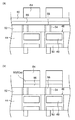
図1は、2層の埋込み配線構造を有する本発明の実施の形態の半導体装置の断面構造を示す。図1に示すように、例えばW(タングステン)からなるプラグ40を有する半導体基板42の絶縁膜43の表面には、例えばSiO2やlow−k膜等の絶縁膜(第1層間絶縁膜)44が堆積されている。そして、この第1層間絶縁膜44の内部に、周囲をバリア層46で包囲した、銅からなる下層配線(第1層の配線)48が、下地膜50の表面に位置して埋設されている。つまり、下層配線48は、下面層46a、周囲層46b及び上面層46cからなるバリア層46によって全周囲を包囲され、この下面層46aは、下地膜50の表面に形成されている。これによって、第1層の配線構造(下層配線構造)が構成されている。
【0031】
下地膜50は、例えば下層配線48の周囲を包囲するバリア層46の下面層46aを無電解めっきで形成するときには触媒層としての役割を、電解めっきで形成する時にはシード層としての役割を果たすもので、例えばPd,Ag,Au,Pt,Co,NiまたはSnの少なくとも1種、またはそれらの合金、この例ではCoから構成されている。また、バリア層46は、下層配線48を保護する配線保護層及び/または配線(銅)48の拡散を防止する拡散防止層としての役割を果たすもので、例えばCo,Co合金,Ni,Ni合金,Ti,Ti合金,TaまたはTa合金、またはそれらの窒化膜、この例ではCoWB合金から構成されている。このことは、下記の下地膜及びバリア層においても同様である。
【0032】
そして、第1層間絶縁膜44の表面に、low−k膜等からなる絶縁膜(第2層間絶縁膜)52が堆積され、この第2層間絶縁膜52の内部に、円筒状で、周囲をバリア層54で包囲した銅からなるビアプラグ56が、下端を前記下層配線48に電気的に接続して埋設されている。
【0033】
そして、この第2層間絶縁膜52の表面に、low−k膜等からなる絶縁膜(第3層間絶縁膜)60が堆積され、この第3層間絶縁膜60の内部に、周囲をバリア層62で包囲した、銅からなる上層配線(第2層の配線)64が、下地膜66の表面に位置し、かつ前記ビアプラグ56に電気的に接続されて埋設されている。つまり、上層配線64は、下面層62a、周囲層62b及び上面層62cからなるバリア層62によって全周囲を包囲され、この下面層62aは、下地膜66の表面に形成されている。これによって、第1層の配線構造の下層配線48とビアプラグ56によって電気的に接続された上層配線64を有する第2層の配線構造(上層配線構造)が構成されている。
【0034】
このように、下層配線48、上層配線64及びビアプラグ56を、CoWB合金等からなり、保護層及び/または銅拡散防止層としての役割を果たすバリア層46,54,62で包囲して保護し、絶縁膜の内部に該絶縁膜のほぼ全域に拡がるSiN等のバリア層を設ける必要をなくして、絶縁膜として実行誘電率を低く抑えることができる。特に、絶縁膜としてlow−k膜を使用した場合に、この効果が顕著となる。
【0035】
次に、図2乃至図10を参照して、図1に示す半導体装置の製造例を工程順に説明する。
先ず、図2(a)に示すように、Wからなるプラグ40を有し、絶縁膜43の表面を必要に応じてCMP等で平坦化した半導体基板42を用意し、この半導体基板42の全表面に、例えばCo膜からなる下地膜50を、例えばスパッタリング(PVD)で形成(成膜)する。この下地膜50は、例えば下記のバリア層70を無電解めっきで形成する場合には触媒層としての、電解めっきで形成する場合にはシード層として役割を果たすもので、PVDの他にCVDや湿式処理、更にはこれらを組み合わせて形成してもよい。
【0036】
この下地膜50をPVDやCVDで形成する場合には、膜厚を、例えば100nm以下とし、湿式処理で形成する場合には、非連続な触媒担持膜とする。
【0037】
次に、図2(b)に示すように、Co層からなる下地膜50の全面に、これを触媒とした無電解めっきで、CoWB合金等からなるバリア層70を形成する。このバリア層70は、Co層からなる下地膜50をシード層とした電解めっきで形成してもよい。またPVDやCVDで、例えばNi合金や他のCo合金等からなる下地膜を成膜するようにしてもよい。
【0038】
そして、図2(c)に示すように、例えばレジスト72を使用して、所定の位置に上下に連通する開口部(トレンチ)72aを有する配線パターンを形成する。この配線パターンは、例えばレジスト塗布、光露光、EB露光及びレジスト現像からなる一連のフォトレジストパターン形成工程によって形成される。
【0039】
次に、図3(a)に示すように、配線パターンのレジスト72で囲まれたトレンチ72a内に、配線材料(銅)を、例えばバリア層70を触媒とした無電解めっきによるボトムアップ成形によって選択的に形成して埋込み、しかる後、必要に応じて、CMPによって余剰な銅を除去し表面を平坦化して、銅からなる下層配線(第1層の配線)48を形成する。この無電解めっきに際し、バリア膜70がCo合金またはNi合金の時には、還元剤としてジメチルアミンボラン(DMAB)等を使用し、下地膜50がPd,Ag,Au,PtまたはSnの時には、還元剤としてグリオキシル酸(GOA)等を使用する。このように、下層配線48を無電解めっきによるボトムアップ成形、つまりボトムの底からめっき膜を成長させて形成することで、下層配線48の内部にボイドが生成されることを防止することができる。このボトムアップ成形による配線材料の埋込みを、電解めっきによって行うようにしてもよい。
【0040】
そして、図3(b)に示すように、バリア層70上の不要なレジスト72を除去する。更に、図3(c)に示すように、絶縁膜43上の余剰なバリア層70と下地膜50を、例えば下層配線48をマスクとして湿式エッチング除去する。これにより、バリア層70で図1に示す下面層46aを構成する。
【0041】
この状態で、下層配線48に、例えば、N2+H2環境下で400℃の30分の熱処理(アニール)を施して、例えば銅からなる下層配線48を再結晶化させることで、下層配線48の比抵抗(ρ)を低下させる。このように、下層配線48を外部に露出させた状態で下層配線48に熱処理を施すことで、下層配線48をダマシン配線構造のように拘束することなく、下層配線48のストレスを緩和させ、これによって、下層配線48のストレスマイグレーション及びエレクトロマイグレーション耐性を向上させることができる。この熱処理(アニール)は、N2+H2雰囲気の他に、N2雰囲気、N2+H2雰囲気、Ar雰囲気、真空雰囲気または還元雰囲気中で行ってもよく、また50〜1000℃の温度に5時間以下晒すことで行われる。
【0042】
次に、図4(a)に示すように、下層配線48を触媒として、下層配線48の露出面全面にバリア層74を無電解めっきで選択的に形成し、これによって、下層配線48の全周囲を前記バリア層70から構成される下面層46a及び該バリア層74で構成される周囲層46b及び上面層46cからなるバリア層46で包囲して下層配線48を保護する。このように、下層配線48の露出面全面にバリア層74を無電解めっきで選択的に形成することで、絶縁膜のほぼ全域に拡がるSiN等のバリア層を設ける必要をなくして、絶縁膜として実行誘電率を低く抑えることができる。なお、このバリア層74は、選択的CVDで形成するようにしてもよい。
【0043】
また、銅からなる配線(下層配線48)にアニール処理を施すと、アニール後の銅配線の表面にアモルファスC膜が形成される。この場合には、無電解めっきの前処理で、H2SO4を用いたエッチング処理を行うことで、このアモルファスC膜をエッチング除去する。
【0044】
そして、図4(b)に示すように、絶縁膜43の表面に、例えば塗布式(スピンコート)でlow−k膜材料を塗布し、この材料をキュアして焼き固めることで、low−k膜等からなる絶縁膜(第1層間絶縁膜)44を形成する。このように、キュアし焼き固めて層間絶縁膜44を形成することで、層間絶縁膜44の強度を高めるとともに、ポーラス状にして内部に空洞を作って、誘電率kを下げることができる。このキュアは、例えば200〜500℃のN2雰囲気中に、基板を0.5〜2時間晒すことで行われる。次に、図4(c)に示すように、第1層間絶縁膜44の表面を、この表面が下層配線48の上面を覆うバリア層46の上面層46cの表面と面一となるまで研磨し平坦化して、第1層の配線構造(下層配線構造)を完成する。
【0045】
そして、図5(a)に示すように、前述の配線パターンとほぼ同様にして、第1層間絶縁膜44と下層配線48の上面を覆うバリア層46の上面層46cの表面に、例えばレジスト76を使用して、所定の位置に上下に連通する開口部(ビアホール)76aを有するビアパターンを形成する。しかる後、図5(b)に示すように、前述とほぼ同様にして、ビアパターンのレジスト76で囲まれたビアホール76a内に、ビア金属(銅)を、例えばビアホール76aの底部のバリア層70を触媒とした無電解めっきによるボトムアップ成形によって選択的に形成して埋込み、しかる後、必要に応じて、CMPによって余剰な銅を除去し表面を平坦化して、銅からなるビアプラグ56を形成する。
【0046】
次に、図5(c)に示すように、第1層間絶縁膜44と下層配線48の上面を覆うバリア層46の上面層46cの表面の不要となったレジスト76を除去する。この状態で、前述と同様に、ビアプラグ56に熱処理(アニール)を施して、ビアプラグ56を構成する銅の比抵抗を低下させるとともに、ストレスマイグレーション及びエレクトロマイグレーション耐性を向上させる。
【0047】
次に、図6(a)に示すように、ビアプラグ56の露出面全面に、ビアプラグ56を触媒とした無電解めっきでバリア層78を選択的に形成し、これによって、ビアプラグ56の周囲をバリア層78で包囲してビアプラグ56を保護するする。このように、ビアプラグ56の露出面全面にバリア層78を無電解めっきで選択的に形成することで、絶縁膜のほぼ全域に拡がるSiN等のバリア層を設ける必要をなくして、絶縁膜として実行誘電率を低く抑えることができることは前述と同様である。
【0048】
そして、図6(b)に示すように、第1層間絶縁膜44及びビアプラグ56を覆うバリア層78の表面に、例えば塗布式(スピンコート)でlow−k膜材料を塗布し、この材料をキュアして焼き固めることで、low−k膜等からなる絶縁膜(第2層間絶縁膜)52を形成する。このように、キュアし焼き固めて層間絶縁膜52を形成することで、層間絶縁膜52の強度を高めるとともに、ポーラス状にして内部に空洞を作って、誘電率kを下げることができることは前述と同様である。次に、図6(c)に示すように、第2層間絶縁膜52の表面を、この表面がビアプラグ56の上面と面一となるまで、ビアプラグ56上のバリア層78のエッチバックを含む研磨を施し平坦化する。これによって、下層配線48の一端と電気的に接続させ、周囲をバリア層78、つまり図1に示すバリア層54で包囲して保護したビアプラグ56を形成する。なお、例えばバリア層78のエッチバックが悪いケースの場合等にあっては、バリア層78の上面と面一となるまで平坦化してもよい。
【0049】
前述のようにして、第1層の配線(下層配線)と該第1層の配線の一端に電気的に接続したビアメタルの形成が終了し、この上に第2層の配線(上層配線)を形成する際には、前述の第1層の配線を形成する時と同じ操作を繰り返し、更にビアプラグを形成する際には、前述のビアプラグを形成する操作を繰り返す。ここでは、更に第2層の配線(上層配線)を形成する例を説明する。
【0050】
すなわち、図7(a)に示すように、第2層間絶縁膜52の全表面に、例えばCoからなる下地膜66を、例えばスパッタリング(PVD)で形成(成膜)する。そして、図7(b)に示すように、この下地膜66の全面に、これを触媒とした無電解めっきで、CoWB合金等からなるバリア層80を形成する。更に、図8(a)に示すように、このバリア層80の表面に、例えばレジスト82を使用して、所定の位置に上下に連通する開口部(トレンチ)82aを有する配線パターンを形成する。次に、図8(b)に示すように、配線パターンのレジスト82で囲まれたトレンチ82a内に、配線材料(銅)を、例えば無電解めっきによるボトムアップ成形によって選択的に形成して埋込み、しかる後、必要に応じて、CMPによって余剰な銅を除去し表面を平坦化して、銅からなる上層配線(第2層の配線)64を形成する。
【0051】
そして、図9(a)に示すように、バリア層80上の不要なレジスト82を、例えば湿式で除去した後、図9(b)に示すように、第2層間絶縁膜52上の余剰なバリア層80と下地膜66を、例えば上層配線64をマスクとして湿式エッチング除去し、これによって、バリア層80で図1に示すバリア層62の下面層62aを構成する。この状態で、上層配線64に、例えば、N2+H2環境下で400℃の30分の熱処理(アニール)を施して、例えば銅からなる上層配線64を再結晶化させることで、上層配線64の比抵抗(ρ)を低下させ、同時に、上層配線64のストレスマイグレーション及びエレクトロマイグレーション耐性を向上させる。
【0052】
そして、図10に示すように、上層配線64の露出面全面にバリア層84を無電解めっきで選択的に形成し、これによって、上層配線64の全周囲を前記バリア層80から構成される下面層62a及び該バリア層84で構成される周囲層62b及び上面層62cからなるバリア層62で包囲して上層配線64を保護する。そして、図示しないが、第2層間絶縁膜52の表面に、例えば塗布式(スピンコート)でlow−k膜材料を塗布し、この材料をキュアして焼き固めることで、low−k膜等からなる絶縁膜(第3層間絶縁膜)60(図1参照)を形成し、この第3層間絶縁膜60の表面を、この表面が上層配線64の上面を覆うバリア層62の上面層62cの表面と面一となるまで研磨し平坦化して、図1に示すように、第2層の配線構造(下層配線構造)を完成する。
【0053】
【実施例】
次に、図1に示す多層配線構造を有する半導体装置を図2乃至図10に示す工程で実際の製造した時の実施例について説明する。先ず、図2(a)に示す、CMP後のプラグ40が露出した絶縁膜43の表面に、スパッタリングにより5nmのCo層からなる下地膜50を形成した。そして、この上に、図2(b)に示すように、この下地膜(Co層)50を触媒として、20nmのCoWB合金膜からなるバリア層70を無電解めっきにより形成した。
【0054】
次に、図2(c)に示すように、フォトレジストパターン成形により、レジスト72で、例えば幅50nm、厚み100nmでAR(アスペスト比)が2.0の開口部(トレンチ)72aをパターン形成した。そして、図3(a)に示すように、バリア層(CoWB合金層)70を触媒とした無電解めっきによる選択的なボトムアップ成形により、トレンチ72aの内部に銅からなる配線材料を埋込んで、銅からなる第1層の配線(下層配線)48を形成した。そして、図3(b)に示すように、不要なレジスト72を除去し、更に図3(c)に示すように、下層配線48をマスクとして、余剰のバリア層(CoWB合金層)70及び下地膜(Co層)50を湿式エッチング除去した。この状態で、下層配線48に、N2+H2環境下で、400℃の30分の熱処理(アニール)を施し、これによって、下層配線48の低抵抗化、ストレス緩和によるストレスマイグレーション及びエレクトロマイグレーション耐性の向上を図った。
【0055】
次に、図4(a)に示すように、下層配線48を触媒として、下層配線48の露出面全面に、CoWB合金膜からなるバリア層74を無電解めっきにより選択的に形成した。そして、図4(b)に示すように、絶縁膜43の表面に、塗布タイプのlow−k膜材料を塗布しキュアして焼き固めたlow−k膜により第1層間絶縁膜44を形成し、しかる後、図4(c)に示すように、下層配線48を覆うバリア層74の上面に合わせて、第1層間絶縁膜44をCMPにより研磨し平坦化した。
【0056】
次に、図5(a)に示すように、フォトレジストパターン成形により、レジスト76で、例えばφ50nm、高さ100nmでAR(アスペスト比)が2.0の開口部(ビアホール)76aをパターン形成した。そして、図5(b)に示すように、ビアホール底のバリア層(CoWB合金層)46(74)を触媒とした無電解めっきによる選択的なボトムアップ成形により、ビアホール76aの内部に銅からなるビア金属を埋込んでビアプラグ56を形成した。そして、図5(c)に示すように、不要なレジスト76を除去した。この状態で、ビアプラグ56に、N2+H2環境下で、400℃の30minの熱処理(アニール)を施し、これによって、ビアプラグ56の低抵抗化、ストレス緩和によるストレスマイグレーション及びエレクトロマイグレーション耐性の向上を図った。
【0057】
次に、図6(a)に示すように、ビアプラグ56を触媒して、ビアプラグ56の露出面全面にCoWB合金膜からなるバリア層78を無電解めっきにより選択的に形成した。そして、図6(b)に示すように、第1層間絶縁膜44の表面に、塗布タイプのlow−k膜材料を塗布しキュアして焼き固めたlow−k膜により第2層間絶縁膜52を形成した。しかる後、図6(c)に示すように、ビアプラグ56の上面を覆うバリア層78のエッチバックを含め、第2層間絶縁膜52の表面をCMPにより研磨し平坦化した。
【0058】
更に、図7(a)に示すように、CMP後の第2層間絶縁膜52及びビアプラグ56の露出面に、スパッタリングにより、5nmのCo膜からなる下地膜66を形成し、更にこの上に、図7(b)に示すように、下地膜(Co層)66を触媒として、20nmのCoWB合金膜からなるバリア層80を無電解めっきにより形成した。そして、図8(a)に示すように、フォトレジストパターン成形により、レジスト82で、例えば幅80nm、厚み160nmでAR(アスペスト比)が2.0の開口部(トレンチ)82aをパターン形成した。そして、図8(b)に示すように、バリア層(CoWB合金層)80を触媒とした無電解めっきによる選択的なボトムアップ成形により、トレンチ82aの内部に銅からなる配線材料を埋込んで、銅からなる第2層の配線(上層配線)64を形成した。
【0059】
そして、図9(a)に示すように、バリア層80上の不要なレジスト82を除去し、更に、図9(b)に示すように、上層配線64をマスクとして、第2層間絶縁膜52上の余剰のバリア層80及び下地膜66を湿式エッチングにより除去した。この状態で、上層配線64に、N2+H2環境下で、400℃の30分の熱処理(アニール)を施し、これによって、上層配線64の低抵抗化、ストレス緩和によるストレスマイグレーション及びエレクトロマイグレーション耐性の向上を図った。
そして、図10に示すように、上層配線64を触媒として、上層配線64の露出面全面に、CoWB合金膜からなるバリア層84を無電解めっきにより選択的に形成した。
【0060】
【発明の効果】
以上詳細に説明したように、本発明によれば、信頼性が高く、かつ配線及びビアプラグの周囲にのみ選択的にバリア層を形成することで、実行誘電率が低い多層配線構造を有する半導体装置を、比較的安価なプロセスにより、容易かつ高いスループットで製造することができる。しかも、選択的なボトムアップめっきにより選択的な埋込みを行うことができ、これによって、デュアルダマシン構造の埋込みめっきとは異なり、ボイドがない信頼性の高い多層配線を形成することができる。
【0061】
更に、デュアルダマシン構造の埋込みめっき配線のアニールと異なり、配線及びビアプラグを開放形状でアニールすることができるので、配線及びビアプラグのストレスを容易に緩和して、ストレスマイグレーション耐性及びエレクトロマイグレーション耐性を向上させることができる。
【図面の簡単な説明】
【図1】本発明の実施の形態における多層配線構造を有する半導体装置の断面図である。
【図2】図1に示す半導体装置の製造工程の配線パターンを形成する迄を工程順に示す断面図である。
【図3】図1に示す半導体装置の製造工程の下層配線を形成する迄を工程順に示す断面図である。
【図4】図1に示す半導体装置の製造工程の第1層絶縁膜の表面を平坦化する迄を工程順に示す断面図である。
【図5】図1に示す半導体装置の製造工程のビアプラグを形成する迄を工程順に示す断面図である。
【図6】図1に示す半導体装置の製造工程の第2層絶縁膜の表面を平坦化する迄を工程順に示す断面図である。
【図7】図1に示す半導体装置の製造工程の上層配線用のバリア層を形成する迄を工程順に示す断面図である。
【図8】図1に示す半導体装置の製造工程の第3層絶縁膜の表面を平坦化する迄を工程順に示す断面図である。
【図9】図1に示す半導体装置の製造工程の上層配線を形成する迄を工程順に示す断面図である。
【図10】図1に示す半導体装置の製造工程の上層配線の露出面全面にバリア層を形成した状態を示す断面図である。
【図11】従来の多層配線構造を有する半導体装置の断面図である。
【符号の説明】
40 プラグ
42 半導体基板
43 絶縁膜
44 第1層間絶縁膜
46,54,62 バリア層
48 下層配線
50,66 下地膜
52 第2層間絶縁膜
56 ビアプラグ
60 第3層間絶縁膜
64 上層配線
70,74,78,80,84 バリア層
72,76,82 レジスト
72a,82a 開口部(トレンチ)
76a 開口部(ビアホール)[0001]
BACKGROUND OF THE INVENTION
The present invention relates to a semiconductor device and a manufacturing method thereof, and more particularly, a via plug in which a lower layer wiring (first layer wiring) and an upper layer wiring (second layer wiring) formed above the lower layer wiring are embedded in a via hole. The present invention relates to a semiconductor device having a multilayer wiring structure electrically connected to each other and a manufacturing method thereof.
[0002]
[Prior art]
As a multilayer wiring formation process of a semiconductor device, a process (so-called dual damascene process) in which metal (conductor) is embedded in wiring trenches and via holes is being used. This is a process in which aluminum, in recent years, copper, silver, or other metal is embedded in wiring trenches and via holes previously formed in the interlayer insulating film, and then the excess metal is removed by chemical mechanical polishing (CMP) and planarized. Technology.
[0003]
In this type of wiring, for example, copper wiring using copper as the wiring material, the surface of the wiring made of copper is exposed to the outside after planarization, preventing thermal diffusion of the wiring (copper), For example, when a semiconductor device having a multilayer wiring structure is formed by laminating an insulating film (oxide film) in an oxidizing atmosphere after that, the wiring formation in which the surface is exposed is used to prevent the wiring (copper) from being oxidized. In general, a barrier layer (wiring protection layer) such as SiN or SiC is formed on the entire surface of the substrate as well as the portion to prevent thermal diffusion and oxidation of the wiring.
[0004]
FIG. 11 shows a general configuration of a conventional multilayer wiring structure composed of copper wiring formed using a dual damascene process. As shown in FIG. 11, for example,
[0005]
Here, the
[0006]
Then, on the upper surface of the
[0007]
The
In addition, the copper wiring is generally recrystallized by subjecting the copper wiring (copper plating film) to heat treatment (annealing) before polishing and removing the excess metal film by CMP.
[0008]
[Problems to be solved by the invention]
However, in the conventional multilayer wiring structure using the dual damascene process, it is generally difficult to uniformly embed a wiring material such as copper into the via holes and the wiring grooves without any spots by electrolytic plating or the like. As shown in FIG. 5, there is a problem that void V is generated inside the wiring, resulting in a decrease in wiring reliability and an increase in wiring resistance, making it difficult to construct a practical process. Moreover, the wiring material is generally embedded by electrolytic plating, and a copper seed layer is formed on the surface of the barrier layer prior to electrolytic plating. This copper seed layer is generally formed by PVD or CVD using an expensive vacuum technique. This leads to an increase in cost. Further, with the miniaturization of wiring, it has been generally difficult to form a thin film seed layer having a uniform thickness.
[0009]
Further, when the
[0010]
Furthermore, the stress of wiring and via plugs embedded in wiring trenches and via holes cannot be relieved, which causes problems of electron migration (EM) and stress migration (SM) and decreases the reliability of wiring. It will lead to.
[0011]
The present invention has been made in view of the above circumstances, and has a multilayer wiring structure with high reliability and low effective dielectric constant, and a semiconductor device that can be easily manufactured by a relatively inexpensive process, and its semiconductor device An object is to provide a manufacturing method.
[0012]
[Means for Solving the Problems]
According to the first aspect of the present invention, the lower layer wiring and the upper layer wiring that are surrounded by the barrier layer are electrically connected by the via plug that is surrounded by the barrier layer, and the wiring and the via plug are placed in the insulating film. The semiconductor device is characterized by being embedded.
As a result, the surroundings of the lower layer wiring, the upper layer wiring and the via plug are surrounded and protected by the barrier layer, and it is not necessary to provide a barrier layer such as SiN which extends almost all over the insulating film inside the insulating film. As a result, the effective dielectric constant can be kept low. In particular, when a low-k film is used as the insulating film, this effect becomes remarkable.
[0013]
The invention according to
[0014]
The invention according to claim 3 is characterized in that the barrier layer is made of Co, Co alloy, Ni, Ni alloy, Ti, Ti alloy, Ta or Ta alloy, or a nitride film thereof. 2. The semiconductor device according to 2. Examples of the Co alloy include CoP, CoB, CoWP, and CoWB alloy. Examples of the Ni alloy include NiP, NiB, NiWP, and NiWB alloy.
[0015]
According to a fourth aspect of the present invention, the barrier layer covering the bottom surface of the wiring is formed on the surface of the base film made of at least one of Pd, Ag, Au, Pt, Co, Ni or Sn, or an alloy thereof. The semiconductor device according to claim 1, wherein the semiconductor device is a semiconductor device.
[0016]
According to a fifth aspect of the present invention, a lower layer wiring surrounded by a barrier layer is formed on the surface of the insulating film so as to protrude from the surface of the insulating film, and a first interlayer insulating film is formed on the surface of the insulating film. Forming the surface of the wiring so as to be exposed, forming a via plug surrounded by a barrier layer on the surface of the lower layer wiring so as to be electrically connected to the lower layer wiring and projecting from the surface of the first interlayer insulating film, A second interlayer insulating film is formed on the surface of the first interlayer insulating film and the lower layer wiring so that the surface of the via plug is exposed, and an upper layer wiring surrounded by a barrier layer on the surface of the second interlayer insulating film is used as the via plug. It is a method for manufacturing a semiconductor device, wherein the semiconductor device is formed by being electrically connected and projecting from the surface of the second interlayer insulating film.
As a result, a semiconductor device having a multilayer wiring structure can be manufactured by a relatively inexpensive process without using a dual damascene process, and the throughput can be improved.
[0017]
According to a sixth aspect of the present invention, in the semiconductor device manufacturing method according to the fifth aspect, the first interlayer insulating film and the second interlayer insulating film are formed by applying an insulating film material and then curing. Is the method.
Thus, by curing and baking and forming the interlayer insulating film, the strength of the interlayer insulating film can be increased, and a cavity can be formed in a porous shape to reduce the dielectric constant k. This cure is, for example, 200-500 ° C N 2 The substrate is exposed to the atmosphere for 0.5 to 2 hours.
The invention described in claim 7 is characterized in that the surface of the first interlayer insulating film and the surface of the second interlayer insulating film after curing are polished to remove excess interlayer insulating film and planarize. Item 7. A method for manufacturing a semiconductor device according to Item 6.
The invention according to claim 8 is the method of manufacturing a semiconductor device according to claim 7, wherein the planarization is performed by CMP.
[0018]
The invention according to claim 9 is characterized in that the wiring and the via plug are made of Cu, Cu alloy, Ag, Ag alloy, Au or Au alloy. It is a manufacturing method.
The invention according to
[0019]
According to an eleventh aspect of the present invention, a base film is formed on the surface of the insulating film, a barrier layer is formed on the surface of the base film, and a wiring pattern is formed with a resist on the surface of the barrier layer. A wiring material is embedded in the wiring to form a wiring made of the wiring material, the resist on the barrier layer, the excess barrier layer and the base film are removed, and the barrier layer is selectively formed on the entire exposed surface of the wiring. 11. The method of manufacturing a semiconductor device according to claim 5, wherein a lower layer wiring and an upper layer wiring are formed to surround the periphery with a barrier layer.
[0020]
According to a twelfth aspect of the present invention, after a wiring material is embedded in the wiring pattern, the surface is polished to remove excess wiring material and planarize the semiconductor device. It is a manufacturing method.
According to a thirteenth aspect of the present invention, in the semiconductor device manufacturing method according to the twelfth aspect, the planarization is performed by CMP.
14. The semiconductor device according to
In this way, the wiring is subjected to heat treatment (annealing) to recrystallize the wiring made of, for example, copper, thereby reducing the specific resistance (ρ) of the wiring and further reducing the stress of the wiring. Electromigration resistance can be improved. This heat treatment is performed, for example, at a temperature of 50 to 1000 ° C. 2 Atmosphere, N 2 + H 2 The substrate is exposed to an atmosphere, an Ar atmosphere, a vacuum atmosphere, or a reducing atmosphere for 5 hours or less.
[0021]
The invention according to claim 15 is characterized in that the base film is made of at least one of Pd, Ag, Au, Pt, Co, Ni, or Sn, or an alloy thereof. A method for manufacturing a semiconductor device according to claim 1.
The base film serves as a seed layer during electroplating and serves as a catalyst layer during electroless plating, and is formed by, for example, PVD, CVD, or wet processing.
[0022]
According to a sixteenth aspect of the present invention, in the semiconductor device according to any one of the eleventh to fifteenth aspects, the embedding of the wiring material is selectively performed by bottom-up molding by electrolytic plating or electroless plating. It is a manufacturing method.
As described above, by forming the wiring by bottom-up molding by plating, that is, by growing the plating film from the bottom of the bottom, it is possible to prevent voids from being generated inside the wiring.
[0023]
The semiconductor device according to any one of
[0024]
The invention according to
As a result, the wiring can be protected by the barrier layer formed on the entire exposed surface of the wiring, and by selectively forming the barrier layer on the entire exposed surface of the wiring, the insulating film such as SiN which extends over almost the entire area can be used. It is not necessary to provide a barrier layer, and the effective dielectric constant as the insulating film can be kept low.
[0025]
According to a nineteenth aspect of the present invention, a via pattern is formed with a resist on the surfaces of the first interlayer insulating film and the lower layer wiring, and a via plug made of the metal is formed by embedding a metal in the via pattern. The resist on the first interlayer insulating film and the lower layer wiring is removed, a barrier layer is selectively formed on the entire exposed surface of the via plug, and a via plug surrounding the periphery with the barrier layer is formed. Item 6. A method for manufacturing a semiconductor device according to Item 5.
[0026]
The invention according to
In this way, the via plug is heat-treated (annealed) to recrystallize the via plug made of, for example, copper, thereby lowering the specific resistance (ρ) of the via plug, further reducing the stress of the via plug, and performing stress migration and electromigration. Migration resistance can be improved. The conditions for this heat treatment are the same as those for the aforementioned wiring.
[0027]
The invention according to claim 21 is the method of manufacturing a semiconductor device according to claim 19 or 20, wherein the metal is selectively embedded by bottom-up molding by electroless plating. Thus, by forming the via plug in bottom-up molding by plating, that is, by growing a plating film from the bottom of the bottom, it is possible to prevent voids from being generated inside the via plug.
[0028]
The invention according to
As a result, the via plug can be protected without increasing the effective dielectric constant as the insulating film by protecting the via plug with the barrier layer selectively formed on the entire exposed surface of the via plug.
[0029]
DETAILED DESCRIPTION OF THE INVENTION
Hereinafter, embodiments of the present invention will be described with reference to the drawings. Although this embodiment shows an example in which copper is used as the wiring material and via material, it goes without saying that materials other than copper may be used as the wiring material and via material.
[0030]
FIG. 1 shows a cross-sectional structure of a semiconductor device according to an embodiment of the present invention having a two-layer buried wiring structure. As shown in FIG. 1, on the surface of the insulating
[0031]
For example, the
[0032]
Then, an insulating film (second interlayer insulating film) 52 made of a low-k film or the like is deposited on the surface of the first
[0033]
Then, an insulating film (third interlayer insulating film) 60 made of a low-k film or the like is deposited on the surface of the second
[0034]
Thus, the
[0035]
Next, an example of manufacturing the semiconductor device shown in FIG. 1 will be described in the order of steps with reference to FIGS.
First, as shown in FIG. 2A, a
[0036]
When this
[0037]
Next, as shown in FIG. 2B, a
[0038]
Then, as shown in FIG. 2C, for example, a resist
[0039]
Next, as shown in FIG. 3A, in the
[0040]
Then, as shown in FIG. 3B, unnecessary resist 72 on the
[0041]
In this state, for example, N 2 + H 2 By performing a heat treatment (annealing) for 30 minutes at 400 ° C. in an environment, the
[0042]
Next, as shown in FIG. 4A, using the
[0043]
Further, when an annealing process is performed on the wiring made of copper (lower layer wiring 48), an amorphous C film is formed on the surface of the annealed copper wiring. In this case, in the pretreatment of electroless plating, 2 SO 4 The amorphous C film is removed by etching using the etching process.
[0044]
Then, as shown in FIG. 4B, a low-k film material is applied to the surface of the insulating
[0045]
Then, as shown in FIG. 5A, a resist 76 is formed on the surface of the
[0046]
Next, as shown in FIG. 5C, the unnecessary resist 76 on the surface of the
[0047]
Next, as shown in FIG. 6A, a
[0048]
Then, as shown in FIG. 6B, a low-k film material is applied to the surface of the
[0049]
As described above, the formation of the first layer wiring (lower layer wiring) and the via metal electrically connected to one end of the first layer wiring is completed, and the second layer wiring (upper layer wiring) is formed thereon. When forming, the same operation as that for forming the first layer wiring is repeated, and when forming a via plug, the operation for forming the via plug is repeated. Here, an example in which a second layer wiring (upper layer wiring) is further formed will be described.
[0050]
That is, as shown in FIG. 7A, a
[0051]
Then, as shown in FIG. 9A, unnecessary resist 82 on the
[0052]
Then, as shown in FIG. 10, a
[0053]
【Example】
Next, an embodiment when the semiconductor device having the multilayer wiring structure shown in FIG. 1 is actually manufactured in the steps shown in FIGS. 2 to 10 will be described. First, a
[0054]
Next, as shown in FIG. 2C, by patterning a photoresist pattern, an opening (trench) 72a having a width of 50 nm, a thickness of 100 nm, and an AR (aspect ratio) of 2.0 is formed by resist pattern molding. . Then, as shown in FIG. 3A, a wiring material made of copper is embedded in the
[0055]
Next, as shown in FIG. 4A, using the
[0056]
Next, as shown in FIG. 5A, by patterning a photoresist pattern, an opening (via hole) 76a having a diameter of 50 nm, a height of 100 nm, and an AR (aspect ratio) of 2.0 is formed by resist pattern molding. . Then, as shown in FIG. 5B, the inside of the via
[0057]
Next, as shown in FIG. 6A, the via
[0058]
Further, as shown in FIG. 7A, a
[0059]
Then, unnecessary resist 82 on the
Then, as shown in FIG. 10, using the
[0060]
【The invention's effect】
As described above in detail, according to the present invention, a semiconductor device having a multilayer wiring structure with high reliability and a low effective dielectric constant by selectively forming a barrier layer only around wiring and via plugs. Can be manufactured easily and with high throughput by a relatively inexpensive process. Moreover, selective embedding can be performed by selective bottom-up plating, which makes it possible to form a highly reliable multi-layer wiring without voids unlike the embedding plating with a dual damascene structure.
[0061]
Furthermore, unlike the annealing of embedded wiring with a dual damascene structure, the wiring and via plugs can be annealed in an open shape, so that stress on the wiring and via plugs can be easily relieved to improve stress migration resistance and electromigration resistance. be able to.
[Brief description of the drawings]
FIG. 1 is a cross-sectional view of a semiconductor device having a multilayer wiring structure in an embodiment of the present invention.
2 is a cross-sectional view showing a sequence of processes until a wiring pattern in a manufacturing process of the semiconductor device shown in FIG. 1 is formed;
3 is a cross-sectional view showing a sequence of steps until a lower layer wiring is formed in the manufacturing process of the semiconductor device shown in FIG. 1;
4 is a cross-sectional view showing steps until the surface of the first insulating film in the manufacturing process of the semiconductor device shown in FIG. 1 is planarized. FIG.
5 is a cross-sectional view showing a sequence of processes until a via plug is formed in the manufacturing process of the semiconductor device shown in FIG. 1. FIG.
6 is a cross-sectional view showing steps until the surface of the second insulating film in the manufacturing process of the semiconductor device shown in FIG. 1 is planarized. FIG.
7 is a cross-sectional view showing, in order of steps, a process until a barrier layer for upper wiring is formed in the manufacturing process of the semiconductor device shown in FIG.
8 is a cross-sectional view showing steps until the surface of a third-layer insulating film in the manufacturing process of the semiconductor device shown in FIG. 1 is planarized.
9 is a cross-sectional view showing a sequence of processes until an upper layer wiring is formed in the manufacturing process of the semiconductor device shown in FIG. 1;
10 is a cross-sectional view showing a state in which a barrier layer is formed on the entire exposed surface of the upper layer wiring in the manufacturing process of the semiconductor device shown in FIG. 1;
FIG. 11 is a cross-sectional view of a semiconductor device having a conventional multilayer wiring structure.
[Explanation of symbols]
40 plugs
42 Semiconductor substrate
43 Insulating film
44 First interlayer insulating film
46, 54, 62 Barrier layer
48 Lower layer wiring
50, 66 Underlayer
52 Second interlayer insulating film
56 Via plug
60 Third interlayer insulating film
64 Upper layer wiring
70, 74, 78, 80, 84 Barrier layer
72,76,82 resist
72a, 82a Opening (trench)
76a Opening (via hole)
Claims (22)
前記絶縁膜の表面に第1層間絶縁膜を前記下層配線の表面を露出させて形成し、
前記下層配線の表面に周囲をバリア層で包囲したビアプラグを前記下層配線に電気的に接続させ前記第1層間絶縁膜の表面から突出させて形成し、
前記第1層間絶縁膜及び下層配線の表面に第2層間絶縁膜を前記ビアプラグの表面を露出させて形成し、
前記第2層間絶縁膜の表面に周囲をバリア層で包囲した上層配線を前記ビアプラグに電気的に接続させ前記第2層間絶縁膜の表面から突出させて形成することを特徴とする半導体装置の製造方法。A lower layer wiring surrounded by a barrier layer on the surface of the insulating film is formed so as to protrude from the surface of the insulating film,
Forming a first interlayer insulating film on the surface of the insulating film, exposing the surface of the lower wiring;
A via plug surrounded by a barrier layer on the surface of the lower wiring is electrically connected to the lower wiring so as to protrude from the surface of the first interlayer insulating film;
Forming a second interlayer insulating film on the surface of the first interlayer insulating film and the lower wiring, exposing the surface of the via plug;
An upper layer wiring surrounded by a barrier layer is formed on the surface of the second interlayer insulating film so as to be electrically connected to the via plug and protrude from the surface of the second interlayer insulating film. Method.
この下地膜の表面にバリア層を形成し、
このバリア層の表面にレジストで配線パターンを形成し、
この配線パターンの内部に配線材料を埋込んで該配線材料からなる配線を形成し、
前記バリア層上のレジスト、余剰なバリア層及び下地膜を除去し、
前記配線の露出面全面にバリア層を選択的に形成して、前記周囲をバリア層で包囲した下層配線及び上層配線をそれぞれ形成することを特徴とする請求項5乃至10のいずれかに記載の半導体装置の製造方法。Forming a base film on the surface of the insulating film;
A barrier layer is formed on the surface of this base film,
Form a wiring pattern with resist on the surface of this barrier layer,
A wiring material is embedded in the wiring pattern to form a wiring made of the wiring material,
Removing the resist, excess barrier layer and underlayer on the barrier layer;
The barrier layer is selectively formed on the entire exposed surface of the wiring, and a lower layer wiring and an upper layer wiring that surround the periphery with a barrier layer are formed, respectively. A method for manufacturing a semiconductor device.
このビアパターンの内部に金属を埋込んで該金属からなるビアプラグを形成し、
前記第1層間絶縁膜上及び下層配線上のレジストを除去し、
前記ビアプラグの露出面全面にバリア層を選択的に形成して前記周囲をバリア層で包囲したビアプラグを形成することを特徴とする請求項5記載の半導体装置の製造方法。Forming a via pattern with a resist on the surface of the first interlayer insulating film and the lower wiring;
A via plug made of the metal is formed by embedding a metal in the via pattern,
Removing the resist on the first interlayer insulating film and the lower wiring;
6. The method of manufacturing a semiconductor device according to claim 5, wherein a barrier layer is selectively formed on the entire exposed surface of the via plug to form a via plug having the periphery surrounded by the barrier layer.
Priority Applications (2)
| Application Number | Priority Date | Filing Date | Title |
|---|---|---|---|
| JP2003198663A JP2005038971A (en) | 2003-07-17 | 2003-07-17 | Semiconductor device and its manufacturing method |
| US10/893,244 US7157370B2 (en) | 2003-07-17 | 2004-07-19 | Semiconductor device and method for manufacturing the same |
Applications Claiming Priority (1)
| Application Number | Priority Date | Filing Date | Title |
|---|---|---|---|
| JP2003198663A JP2005038971A (en) | 2003-07-17 | 2003-07-17 | Semiconductor device and its manufacturing method |
Publications (2)
| Publication Number | Publication Date |
|---|---|
| JP2005038971A true JP2005038971A (en) | 2005-02-10 |
| JP2005038971A5 JP2005038971A5 (en) | 2006-08-24 |
Family
ID=34113600
Family Applications (1)
| Application Number | Title | Priority Date | Filing Date |
|---|---|---|---|
| JP2003198663A Withdrawn JP2005038971A (en) | 2003-07-17 | 2003-07-17 | Semiconductor device and its manufacturing method |
Country Status (2)
| Country | Link |
|---|---|
| US (1) | US7157370B2 (en) |
| JP (1) | JP2005038971A (en) |
Cited By (2)
| Publication number | Priority date | Publication date | Assignee | Title |
|---|---|---|---|---|
| JP2013145899A (en) * | 2006-05-22 | 2013-07-25 | Samsung Electronics Co Ltd | Semiconductor integrated circuit element having mim capacitor, and method of manufacturing the same |
| JP2014236177A (en) * | 2013-06-05 | 2014-12-15 | 日本電信電話株式会社 | Wiring structure and formation method thereof |
Families Citing this family (24)
| Publication number | Priority date | Publication date | Assignee | Title |
|---|---|---|---|---|
| CN1327508C (en) * | 2003-04-28 | 2007-07-18 | 富士通株式会社 | Manufacture of semiconductor device |
| JP2006202852A (en) * | 2005-01-18 | 2006-08-03 | Toshiba Corp | Semiconductor device |
| US7138714B2 (en) * | 2005-02-11 | 2006-11-21 | International Business Machines Corporation | Via barrier layers continuous with metal line barrier layers at notched or dielectric mesa portions in metal lines |
| TWI256105B (en) * | 2005-02-17 | 2006-06-01 | Touch Micro System Tech | Method of forming chip type low-k dielectric layer |
| US7913644B2 (en) * | 2005-09-30 | 2011-03-29 | Lam Research Corporation | Electroless deposition system |
| US7592211B2 (en) * | 2006-01-17 | 2009-09-22 | Cree, Inc. | Methods of fabricating transistors including supported gate electrodes |
| US7709269B2 (en) * | 2006-01-17 | 2010-05-04 | Cree, Inc. | Methods of fabricating transistors including dielectrically-supported gate electrodes |
| DE102006004429A1 (en) * | 2006-01-31 | 2007-08-02 | Advanced Micro Devices, Inc., Sunnyvale | Forming metallization layers for high-density integrated circuit component interconnection, also deposits dielectric material of low permitivity |
| WO2007089495A1 (en) * | 2006-01-31 | 2007-08-09 | Advanced Micro Devices, Inc. | A semiconductor device comprising a metallization layer stack with a porous low-k material having an enhanced integrity |
| KR100727691B1 (en) * | 2006-06-20 | 2007-06-13 | 동부일렉트로닉스 주식회사 | Method for forming semiconductor device metal-wiring |
| US20080054466A1 (en) * | 2006-08-31 | 2008-03-06 | Kabushiki Kaisha Toshiba | Semiconductor device and method of manufacturing semiconductor device |
| JP4539684B2 (en) * | 2007-06-21 | 2010-09-08 | 株式会社デンソー | Silicon carbide semiconductor device and manufacturing method thereof |
| KR20130092570A (en) * | 2010-08-31 | 2013-08-20 | 도쿄엘렉트론가부시키가이샤 | Method for manufacturing semiconductor device |
| US8518818B2 (en) | 2011-09-16 | 2013-08-27 | Taiwan Semiconductor Manufacturing Co., Ltd. | Reverse damascene process |
| US9209082B2 (en) * | 2014-01-03 | 2015-12-08 | International Business Machines Corporation | Methods of localized hardening of dicing channel by applying localized heat in wafer kerf |
| SG11201610662QA (en) * | 2014-07-25 | 2017-01-27 | Intel Corp | Tungsten alloys in semiconductor devices |
| US9431343B1 (en) | 2015-03-11 | 2016-08-30 | Samsung Electronics Co., Ltd. | Stacked damascene structures for microelectronic devices |
| CN106409754B (en) * | 2015-07-29 | 2020-03-10 | 中芯国际集成电路制造(上海)有限公司 | Semiconductor structure and manufacturing method thereof |
| WO2017087005A1 (en) * | 2015-11-21 | 2017-05-26 | Intel Corporation | Metallization stacks with enclosed vias |
| US9899260B2 (en) * | 2016-01-21 | 2018-02-20 | Micron Technology, Inc. | Method for fabricating a semiconductor device |
| US10535560B2 (en) * | 2017-07-18 | 2020-01-14 | Taiwan Semiconductor Manufacturing Co., Ltd. | Interconnection structure of semiconductor device |
| CN109411406A (en) * | 2017-08-18 | 2019-03-01 | 中芯国际集成电路制造(上海)有限公司 | Semiconductor structure and forming method thereof |
| US10600656B2 (en) * | 2017-11-21 | 2020-03-24 | International Business Machines Corporation | Directed self-assembly for copper patterning |
| WO2019135985A1 (en) * | 2018-01-03 | 2019-07-11 | Corning Incorporated | Methods for making electrodes and providing electrical connections in sensors |
Family Cites Families (9)
| Publication number | Priority date | Publication date | Assignee | Title |
|---|---|---|---|---|
| US5674787A (en) | 1996-01-16 | 1997-10-07 | Sematech, Inc. | Selective electroless copper deposited interconnect plugs for ULSI applications |
| US5695810A (en) | 1996-11-20 | 1997-12-09 | Cornell Research Foundation, Inc. | Use of cobalt tungsten phosphide as a barrier material for copper metallization |
| US6114243A (en) | 1999-11-15 | 2000-09-05 | Chartered Semiconductor Manufacturing Ltd | Method to avoid copper contamination on the sidewall of a via or a dual damascene structure |
| US6815329B2 (en) * | 2000-02-08 | 2004-11-09 | International Business Machines Corporation | Multilayer interconnect structure containing air gaps and method for making |
| US6555909B1 (en) * | 2001-01-11 | 2003-04-29 | Advanced Micro Devices, Inc. | Seedless barrier layers in integrated circuits and a method of manufacture therefor |
| US6555467B2 (en) * | 2001-09-28 | 2003-04-29 | Sharp Laboratories Of America, Inc. | Method of making air gaps copper interconnect |
| JP3778045B2 (en) * | 2001-10-09 | 2006-05-24 | 三菱電機株式会社 | Manufacturing method of low dielectric constant material, low dielectric constant material, insulating film and semiconductor device using the low dielectric constant material |
| JP4555540B2 (en) * | 2002-07-08 | 2010-10-06 | ルネサスエレクトロニクス株式会社 | Semiconductor device |
| TWI313066B (en) * | 2003-02-11 | 2009-08-01 | United Microelectronics Corp | Capacitor in an interconnect system and method of manufacturing thereof |
-
2003
- 2003-07-17 JP JP2003198663A patent/JP2005038971A/en not_active Withdrawn
-
2004
- 2004-07-19 US US10/893,244 patent/US7157370B2/en active Active
Cited By (2)
| Publication number | Priority date | Publication date | Assignee | Title |
|---|---|---|---|---|
| JP2013145899A (en) * | 2006-05-22 | 2013-07-25 | Samsung Electronics Co Ltd | Semiconductor integrated circuit element having mim capacitor, and method of manufacturing the same |
| JP2014236177A (en) * | 2013-06-05 | 2014-12-15 | 日本電信電話株式会社 | Wiring structure and formation method thereof |
Also Published As
| Publication number | Publication date |
|---|---|
| US7157370B2 (en) | 2007-01-02 |
| US20050029669A1 (en) | 2005-02-10 |
Similar Documents
| Publication | Publication Date | Title |
|---|---|---|
| JP2005038971A (en) | Semiconductor device and its manufacturing method | |
| KR100550304B1 (en) | Borderless vias with hsq gap filled patterned metal layers | |
| US20040004288A1 (en) | Semiconductor device and manufacturing method of the same | |
| JP4790972B2 (en) | Hybrid low dielectric constant interconnect structure composed of two spin-on dielectric materials | |
| US7834459B2 (en) | Semiconductor device and semiconductor device manufacturing method | |
| JP3182608B2 (en) | Method of forming contact plug of semiconductor device having contact holes of different sizes | |
| TWI260740B (en) | Semiconductor device with low-resistance inlaid copper/barrier interconnects and method for manufacturing the same | |
| US20040043598A1 (en) | Method for creating a damascene interconnect using a two-step electroplating process | |
| JP2000077411A (en) | Semiconductor device and manufacture thereof | |
| JP2005038971A5 (en) | ||
| TWI513378B (en) | Method and structure to improve the conductivity of narrow copper filled vias | |
| US6046106A (en) | High density plasma oxide gap filled patterned metal layers with improved electromigration resistance | |
| US8404577B2 (en) | Semiconductor device having a grain orientation layer | |
| US6225226B1 (en) | Method for processing and integrating copper interconnects | |
| US20070072413A1 (en) | Methods of forming copper interconnect structures on semiconductor substrates | |
| US20020127849A1 (en) | Method of manufacturing dual damascene structure | |
| US7572717B2 (en) | Method of manufacturing semiconductor device | |
| JP2006196642A (en) | Semiconductor device and its manufacturing method | |
| US20070178690A1 (en) | Semiconductor device comprising a metallization layer stack with a porous low-k material having an enhanced integrity | |
| KR100945503B1 (en) | Method for forming metal interconnection layer of semiconductor device | |
| JP3939270B2 (en) | Method for forming wiring structure | |
| JP4152164B2 (en) | Manufacturing method of semiconductor device | |
| US6403474B1 (en) | Controlled anneal conductors for integrated circuit interconnects | |
| JP4064595B2 (en) | Manufacturing method of semiconductor device | |
| KR100833451B1 (en) | Method of forming a copper wiring in a semiconductor device |
Legal Events
| Date | Code | Title | Description |
|---|---|---|---|
| A521 | Written amendment |
Free format text: JAPANESE INTERMEDIATE CODE: A523 Effective date: 20060710 |
|
| A621 | Written request for application examination |
Free format text: JAPANESE INTERMEDIATE CODE: A621 Effective date: 20060710 |
|
| A761 | Written withdrawal of application |
Free format text: JAPANESE INTERMEDIATE CODE: A761 Effective date: 20070713 |