JP5179077B2 - 投影露光装置の照明デバイスの光学システム - Google Patents
投影露光装置の照明デバイスの光学システム Download PDFInfo
- Publication number
- JP5179077B2 JP5179077B2 JP2007064831A JP2007064831A JP5179077B2 JP 5179077 B2 JP5179077 B2 JP 5179077B2 JP 2007064831 A JP2007064831 A JP 2007064831A JP 2007064831 A JP2007064831 A JP 2007064831A JP 5179077 B2 JP5179077 B2 JP 5179077B2
- Authority
- JP
- Japan
- Prior art keywords
- optical system
- photoconductive
- optical
- doe
- structures
- Prior art date
- Legal status (The legal status is an assumption and is not a legal conclusion. Google has not performed a legal analysis and makes no representation as to the accuracy of the status listed.)
- Active
Links
- 230000003287 optical effect Effects 0.000 title claims description 160
- 238000005286 illumination Methods 0.000 title claims description 17
- 239000013078 crystal Substances 0.000 claims description 94
- 239000000463 material Substances 0.000 claims description 91
- 230000010287 polarization Effects 0.000 claims description 53
- 239000000758 substrate Substances 0.000 claims description 34
- 230000000694 effects Effects 0.000 claims description 13
- 238000004519 manufacturing process Methods 0.000 claims description 2
- 238000000034 method Methods 0.000 claims 2
- VYPSYNLAJGMNEJ-UHFFFAOYSA-N Silicium dioxide Chemical compound O=[Si]=O VYPSYNLAJGMNEJ-UHFFFAOYSA-N 0.000 description 23
- 238000009826 distribution Methods 0.000 description 16
- 239000002178 crystalline material Substances 0.000 description 9
- TWNQGVIAIRXVLR-UHFFFAOYSA-N oxo(oxoalumanyloxy)alumane Chemical compound O=[Al]O[Al]=O TWNQGVIAIRXVLR-UHFFFAOYSA-N 0.000 description 7
- 239000010453 quartz Substances 0.000 description 7
- 238000005530 etching Methods 0.000 description 5
- -1 fluoride compound Chemical class 0.000 description 5
- ORUIBWPALBXDOA-UHFFFAOYSA-L magnesium fluoride Chemical compound [F-].[F-].[Mg+2] ORUIBWPALBXDOA-UHFFFAOYSA-L 0.000 description 5
- 210000001747 pupil Anatomy 0.000 description 5
- WUKWITHWXAAZEY-UHFFFAOYSA-L calcium difluoride Chemical compound [F-].[F-].[Ca+2] WUKWITHWXAAZEY-UHFFFAOYSA-L 0.000 description 4
- 150000001875 compounds Chemical class 0.000 description 4
- CPLXHLVBOLITMK-UHFFFAOYSA-N magnesium oxide Inorganic materials [Mg]=O CPLXHLVBOLITMK-UHFFFAOYSA-N 0.000 description 4
- 239000000395 magnesium oxide Substances 0.000 description 4
- AXZKOIWUVFPNLO-UHFFFAOYSA-N magnesium;oxygen(2-) Chemical compound [O-2].[Mg+2] AXZKOIWUVFPNLO-UHFFFAOYSA-N 0.000 description 4
- BYMUNNMMXKDFEZ-UHFFFAOYSA-K trifluorolanthanum Chemical compound F[La](F)F BYMUNNMMXKDFEZ-UHFFFAOYSA-K 0.000 description 4
- 238000003491 array Methods 0.000 description 3
- 230000008901 benefit Effects 0.000 description 3
- 230000008859 change Effects 0.000 description 3
- 230000007423 decrease Effects 0.000 description 3
- 230000007547 defect Effects 0.000 description 3
- 238000010586 diagram Methods 0.000 description 3
- 230000003993 interaction Effects 0.000 description 3
- 230000005855 radiation Effects 0.000 description 3
- 230000009471 action Effects 0.000 description 2
- 239000011149 active material Substances 0.000 description 2
- 238000007654 immersion Methods 0.000 description 2
- 239000007788 liquid Substances 0.000 description 2
- 230000000873 masking effect Effects 0.000 description 2
- 238000001393 microlithography Methods 0.000 description 2
- 238000012986 modification Methods 0.000 description 2
- 230000004048 modification Effects 0.000 description 2
- 238000005457 optimization Methods 0.000 description 2
- 238000000059 patterning Methods 0.000 description 2
- FVRNDBHWWSPNOM-UHFFFAOYSA-L strontium fluoride Chemical compound [F-].[F-].[Sr+2] FVRNDBHWWSPNOM-UHFFFAOYSA-L 0.000 description 2
- 229910001637 strontium fluoride Inorganic materials 0.000 description 2
- 230000007704 transition Effects 0.000 description 2
- 238000011144 upstream manufacturing Methods 0.000 description 2
- 238000007740 vapor deposition Methods 0.000 description 2
- 229910018072 Al 2 O 3 Inorganic materials 0.000 description 1
- 101100495531 Caenorhabditis elegans cgh-1 gene Proteins 0.000 description 1
- 229910017768 LaF 3 Inorganic materials 0.000 description 1
- 229910020068 MgAl Inorganic materials 0.000 description 1
- 238000010521 absorption reaction Methods 0.000 description 1
- 230000002411 adverse Effects 0.000 description 1
- 229910001634 calcium fluoride Inorganic materials 0.000 description 1
- 230000006378 damage Effects 0.000 description 1
- 230000001419 dependent effect Effects 0.000 description 1
- 230000005684 electric field Effects 0.000 description 1
- 230000002708 enhancing effect Effects 0.000 description 1
- 230000004907 flux Effects 0.000 description 1
- 230000014509 gene expression Effects 0.000 description 1
- 150000002500 ions Chemical class 0.000 description 1
- 239000000203 mixture Substances 0.000 description 1
- 230000000737 periodic effect Effects 0.000 description 1
- 230000002441 reversible effect Effects 0.000 description 1
- 239000004065 semiconductor Substances 0.000 description 1
Images


Classifications
-
- G—PHYSICS
- G03—PHOTOGRAPHY; CINEMATOGRAPHY; ANALOGOUS TECHNIQUES USING WAVES OTHER THAN OPTICAL WAVES; ELECTROGRAPHY; HOLOGRAPHY
- G03F—PHOTOMECHANICAL PRODUCTION OF TEXTURED OR PATTERNED SURFACES, e.g. FOR PRINTING, FOR PROCESSING OF SEMICONDUCTOR DEVICES; MATERIALS THEREFOR; ORIGINALS THEREFOR; APPARATUS SPECIALLY ADAPTED THEREFOR
- G03F7/00—Photomechanical, e.g. photolithographic, production of textured or patterned surfaces, e.g. printing surfaces; Materials therefor, e.g. comprising photoresists; Apparatus specially adapted therefor
- G03F7/70—Microphotolithographic exposure; Apparatus therefor
- G03F7/70058—Mask illumination systems
- G03F7/70075—Homogenization of illumination intensity in the mask plane by using an integrator, e.g. fly's eye lens, facet mirror or glass rod, by using a diffusing optical element or by beam deflection
-
- G—PHYSICS
- G02—OPTICS
- G02B—OPTICAL ELEMENTS, SYSTEMS OR APPARATUS
- G02B1/00—Optical elements characterised by the material of which they are made; Optical coatings for optical elements
- G02B1/02—Optical elements characterised by the material of which they are made; Optical coatings for optical elements made of crystals, e.g. rock-salt, semi-conductors
-
- G—PHYSICS
- G02—OPTICS
- G02B—OPTICAL ELEMENTS, SYSTEMS OR APPARATUS
- G02B1/00—Optical elements characterised by the material of which they are made; Optical coatings for optical elements
- G02B1/08—Optical elements characterised by the material of which they are made; Optical coatings for optical elements made of polarising materials
-
- G—PHYSICS
- G02—OPTICS
- G02B—OPTICAL ELEMENTS, SYSTEMS OR APPARATUS
- G02B3/00—Simple or compound lenses
- G02B3/0006—Arrays
- G02B3/0037—Arrays characterized by the distribution or form of lenses
- G02B3/005—Arrays characterized by the distribution or form of lenses arranged along a single direction only, e.g. lenticular sheets
-
- G—PHYSICS
- G02—OPTICS
- G02B—OPTICAL ELEMENTS, SYSTEMS OR APPARATUS
- G02B3/00—Simple or compound lenses
- G02B3/0006—Arrays
- G02B3/0037—Arrays characterized by the distribution or form of lenses
- G02B3/0062—Stacked lens arrays, i.e. refractive surfaces arranged in at least two planes, without structurally separate optical elements in-between
- G02B3/0068—Stacked lens arrays, i.e. refractive surfaces arranged in at least two planes, without structurally separate optical elements in-between arranged in a single integral body or plate, e.g. laminates or hybrid structures with other optical elements
-
- G—PHYSICS
- G02—OPTICS
- G02B—OPTICAL ELEMENTS, SYSTEMS OR APPARATUS
- G02B5/00—Optical elements other than lenses
- G02B5/18—Diffraction gratings
- G02B5/1814—Diffraction gratings structurally combined with one or more further optical elements, e.g. lenses, mirrors, prisms or other diffraction gratings
- G02B5/1819—Plural gratings positioned on the same surface, e.g. array of gratings
- G02B5/1823—Plural gratings positioned on the same surface, e.g. array of gratings in an overlapping or superposed manner
-
- G—PHYSICS
- G02—OPTICS
- G02B—OPTICAL ELEMENTS, SYSTEMS OR APPARATUS
- G02B5/00—Optical elements other than lenses
- G02B5/18—Diffraction gratings
- G02B5/1833—Diffraction gratings comprising birefringent materials
-
- G—PHYSICS
- G02—OPTICS
- G02B—OPTICAL ELEMENTS, SYSTEMS OR APPARATUS
- G02B5/00—Optical elements other than lenses
- G02B5/18—Diffraction gratings
- G02B5/1838—Diffraction gratings for use with ultraviolet radiation or X-rays
-
- G—PHYSICS
- G02—OPTICS
- G02B—OPTICAL ELEMENTS, SYSTEMS OR APPARATUS
- G02B5/00—Optical elements other than lenses
- G02B5/18—Diffraction gratings
- G02B5/1866—Transmission gratings characterised by their structure, e.g. step profile, contours of substrate or grooves, pitch variations, materials
-
- G—PHYSICS
- G03—PHOTOGRAPHY; CINEMATOGRAPHY; ANALOGOUS TECHNIQUES USING WAVES OTHER THAN OPTICAL WAVES; ELECTROGRAPHY; HOLOGRAPHY
- G03B—APPARATUS OR ARRANGEMENTS FOR TAKING PHOTOGRAPHS OR FOR PROJECTING OR VIEWING THEM; APPARATUS OR ARRANGEMENTS EMPLOYING ANALOGOUS TECHNIQUES USING WAVES OTHER THAN OPTICAL WAVES; ACCESSORIES THEREFOR
- G03B27/00—Photographic printing apparatus
- G03B27/72—Controlling or varying light intensity, spectral composition, or exposure time in photographic printing apparatus
-
- G—PHYSICS
- G03—PHOTOGRAPHY; CINEMATOGRAPHY; ANALOGOUS TECHNIQUES USING WAVES OTHER THAN OPTICAL WAVES; ELECTROGRAPHY; HOLOGRAPHY
- G03F—PHOTOMECHANICAL PRODUCTION OF TEXTURED OR PATTERNED SURFACES, e.g. FOR PRINTING, FOR PROCESSING OF SEMICONDUCTOR DEVICES; MATERIALS THEREFOR; ORIGINALS THEREFOR; APPARATUS SPECIALLY ADAPTED THEREFOR
- G03F7/00—Photomechanical, e.g. photolithographic, production of textured or patterned surfaces, e.g. printing surfaces; Materials therefor, e.g. comprising photoresists; Apparatus specially adapted therefor
- G03F7/70—Microphotolithographic exposure; Apparatus therefor
- G03F7/70058—Mask illumination systems
- G03F7/7015—Details of optical elements
- G03F7/70158—Diffractive optical elements
-
- G—PHYSICS
- G03—PHOTOGRAPHY; CINEMATOGRAPHY; ANALOGOUS TECHNIQUES USING WAVES OTHER THAN OPTICAL WAVES; ELECTROGRAPHY; HOLOGRAPHY
- G03F—PHOTOMECHANICAL PRODUCTION OF TEXTURED OR PATTERNED SURFACES, e.g. FOR PRINTING, FOR PROCESSING OF SEMICONDUCTOR DEVICES; MATERIALS THEREFOR; ORIGINALS THEREFOR; APPARATUS SPECIALLY ADAPTED THEREFOR
- G03F7/00—Photomechanical, e.g. photolithographic, production of textured or patterned surfaces, e.g. printing surfaces; Materials therefor, e.g. comprising photoresists; Apparatus specially adapted therefor
- G03F7/70—Microphotolithographic exposure; Apparatus therefor
- G03F7/70483—Information management; Active and passive control; Testing; Wafer monitoring, e.g. pattern monitoring
- G03F7/7055—Exposure light control in all parts of the microlithographic apparatus, e.g. pulse length control or light interruption
- G03F7/70566—Polarisation control
-
- G—PHYSICS
- G03—PHOTOGRAPHY; CINEMATOGRAPHY; ANALOGOUS TECHNIQUES USING WAVES OTHER THAN OPTICAL WAVES; ELECTROGRAPHY; HOLOGRAPHY
- G03F—PHOTOMECHANICAL PRODUCTION OF TEXTURED OR PATTERNED SURFACES, e.g. FOR PRINTING, FOR PROCESSING OF SEMICONDUCTOR DEVICES; MATERIALS THEREFOR; ORIGINALS THEREFOR; APPARATUS SPECIALLY ADAPTED THEREFOR
- G03F7/00—Photomechanical, e.g. photolithographic, production of textured or patterned surfaces, e.g. printing surfaces; Materials therefor, e.g. comprising photoresists; Apparatus specially adapted therefor
- G03F7/70—Microphotolithographic exposure; Apparatus therefor
- G03F7/708—Construction of apparatus, e.g. environment aspects, hygiene aspects or materials
- G03F7/7095—Materials, e.g. materials for housing, stage or other support having particular properties, e.g. weight, strength, conductivity, thermal expansion coefficient
- G03F7/70958—Optical materials or coatings, e.g. with particular transmittance, reflectance or anti-reflection properties
- G03F7/70966—Birefringence
Landscapes
- Physics & Mathematics (AREA)
- General Physics & Mathematics (AREA)
- Optics & Photonics (AREA)
- Health & Medical Sciences (AREA)
- Engineering & Computer Science (AREA)
- Environmental & Geological Engineering (AREA)
- Epidemiology (AREA)
- Public Health (AREA)
- Chemical & Material Sciences (AREA)
- Crystallography & Structural Chemistry (AREA)
- Spectroscopy & Molecular Physics (AREA)
- Toxicology (AREA)
- Exposure And Positioning Against Photoresist Photosensitive Materials (AREA)
- Optical Elements Other Than Lenses (AREA)
- Holo Graphy (AREA)
- Exposure Of Semiconductors, Excluding Electron Or Ion Beam Exposure (AREA)
Description
本発明は、マイクロリソグラフィ投影露光装置の照明デバイスの光学システムに関する。このシステムは少なくとも1つの光伝導性増大部材(light-conductance-increasing element)を含む。この光伝導性増大部材では、偏光状態を維持しながら、光伝導性を得ることが可能である。
マイクロリソグラフィ投影露光装置の照明デバイスでは、しばしば回折性光学素子(DOEs)が入口で使用され、所望の強度(輝度)分布(例えば二重極分布または四重極分布)が形成される。これには、例えば瞳面内の各回折表面構造によって定められる、DOEの角度放射特性が用いられる。
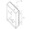
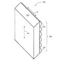
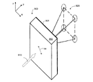
図1は、本発明の第1の実施例に相応した、光伝導性増大部材100を示している。
Claims (39)
- マイクロリソグラフィ投影露光装置の照明デバイスの光学システムであって、当該光学システムは、
・少なくとも1つの第1の光伝導性増大部材(100、200、300a、400、500a、900)を含み、当該第1の光伝導性増大部材は複数の回折性または屈折性ビーム偏光構造体を有しており、当該構造体は共通の第1の優先方向(D1)に延在しており;
・前記光伝導性増大部材は光学的単軸結晶材料を有しており、当該結晶材料の光学結晶軸は、前記第1の優先方向(D1)に対して実質的に平行であるか、または実質的に垂直であり、
前記光学結晶軸は、当該光学システムの作動時に、前記部材に入射する光の光伝播方向に垂直である、
ことを特徴とする、マイクロリソグラフィ投影露光装置の照明デバイスの光学システム。 - 前記光学結晶軸が、前記光伝導性増大部材に入射する光の偏光の優先方向に対して、実質的に平行であるか、または実質的に垂直であるように前記光伝導性増大部材が配置されている、請求項1記載の光学システム。
- 前記ビーム偏光構造体が基板上に形成されており、当該基板は光学的単軸結晶材料から成り、
当該結晶材料の光学結晶軸は前記基板の表面に対して実質的に平行に配向されている、請求項1または2記載の光学システム。 - 前記第1の光伝導性増大部材の複数のビーム偏光構造体は、円柱レンズ(121、221、321、421、511)の配列によって形成されている、請求項1から3までのいずれか1項記載の光学システム。
- 前記第1の光伝導性増大部材の複数のビーム偏光構造体は、回折性光学部材(DOE)によって形成されている、請求項1から3までのいずれか1項記載の光学システム。
- 前記回折性光学部材(DOE)は計算機ホログラム(CGH)である、請求項5記載の光学システム。
- 前記計算機ホログラム(CGH)はファセット領域のアレイを含んでいる、請求項6記載の光学システム。
- 前記計算機ホログラム(CGH)のビーム偏光構造が隣接するファセット領域の間の境界にわたって非連続性を含むように前記ファセット領域のアレイは形成されている、請求項7記載の光学システム。
- 前記計算機ホログラム(CGH)のビーム偏光構造が隣接するファセット領域の間の境界にわたって非連続性を含まないように前記ファセット領域のアレイは形成されている、請求項7記載の光学システム。
- 前記計算機ホログラム(CGH)のビーム偏光構造が前記ファセット領域の少なくとも1つのファセット領域において模写されるように、前記ファセット領域のアレイは形成されている、請求項7から9までのいずれか1項記載の光学システム。
- 前記計算機ホログラム(CGH)のビーム偏光構造が前記ファセット領域のいずれのファセット領域においても模写されないように、前記ファセット領域のアレイは形成されている、前記請求項7から9までのいずれか1項記載の光学システム。
- 前記ファセット領域は多角形形状を有しており、相互に隣接して対になって配置されている、請求項7から11までのいずれか1項記載の光学システム。
- 前記多角形形状は、三角形、長方形、正方形および六角形から成るグループから選択される、請求項12記載の光学システム。
- 前記ファセット領域は相互に隣接しており、その断面に関して類似している、請求項7から13までのいずれか1項記載の光学システム。
- 前記ファセット領域は相互に隣接しており、異なる断面を有している、請求項7から13までのいずれか1項記載の光学システム。
- 前記回折性光学部材(DOE)は少なくとも1つのブレーズ格子を有している、請求項5記載の光学システム。
- 相互に直交する2つの偏光状態のうちの1つに対して、他方の偏光状態に対してよりも、ブレーズ作用がより大きくなるように前記回折性光学部材(DOE)は形成されている、請求項16記載の光学システム。
- 前記回折性光学部材(DOE)は第1のブレーズ格子(810)および少なくとも1つの第2のブレーズ格子(820)を有しており、
当該ブレーズ格子のうちの少なくとも1つの格子構造は、回折性光学部材(DOE)が設計されている動作波長よりも小さい、請求項16または17記載の光学システム。 - 前記第2のブレーズ格子(820)の格子構造は、前記第1のブレーズ格子(810)上に形成されている、請求項18記載の光学システム。
- 前記第2のブレーズ格子(820)は、前記第1のブレーズ格子(810)の光出射表面上に重畳されている、請求項19記載の光学システム。
- 前記ブレーズ格子の少なくとも1つ(820)は実質的にリブが付けられた構造を有している、請求項18から20までのいずれか1項記載の光学システム。
- 前記第1のブレーズ格子(810)は実質的には階段状の幾何学的形状を有しているか、または実質的に鋸歯状の幾何学的形状を有している、請求項18から21までのいずれか1項記載の光学システム。
- 前記第2のブレーズ格子(820)はサブ構造体(820a〜820e)から形成されており、当該サブ構造体は相互に並んで延在方向(D)に沿って配列されており、前記回折性光学部材(DOE)が設計されている動作波長よりも小さい、請求項18から22までのいずれか1項記載の光学システム。
- 前記サブ構造体(820a〜820e)は、前記第1のブレーズ格子(810)の実質的に階段状の領域または実質的に鋸の歯状の領域上に形成されている、請求項23記載の光学システム。
- 前記サブ構造体(820a〜820e)の配列は、前記延在方向(D)において変化する、請求項23または24記載の光学システム。
- 前記サブ構造体(820a〜820e)の配置は、前記延在方向(D)に対して垂直に変化する、請求項23から25のうちのいずれか1項記載の光学システム。
- 前記サブ構造体(820a〜820e)の充填比は前記延在方向(D)に沿って一定である、請求項23から26までのいずれか1項記載の光学システム。
- 第2の光伝導性増大部材(300b,500b)は光伝播方向において前記第1の光伝導性増大部材(300a,500a)の下流に配置されており、
複数の回折性または屈折性のビーム偏光構造を有しており、
当該ビーム偏光構造は第2の優先方向に延在しており、当該第2の優先方向は第1の優先方向とは異なっている、請求項1から27までのいずれか1項記載の光学システム。 - 前記第2の優先方向(D2)は、前記第1の優先方向(D1)に対して実質的に垂直である、請求項28記載の光学システム。
- 前記第2の光伝導性増大部材(300b,500b)は少なくともビーム偏光構造体の領域において、光学的等方性材料から製造されている、請求項28または29記載の光学システム。
- 前記第2の光伝導性増大部材(300b,500b)のビーム偏光構造体は、光学的単軸結晶材料から成る基板(530)上に形成されている、請求項28から30までのいずれか1項記載の光学システム。
- 前記第2の光伝導性増大部材の結晶材料の光学結晶軸は前記第2の優先方向に対して実質的に平行であるか、または実質的に垂直である、請求項28から31までのいずれか1項記載の光学システム。
- 第1の光混合デバイスが、前記第1の光伝導性増大部材(500a)と前記第2の光伝導性増大部材(500b)の間に配置されている、請求項28から32までのいずれか1項記載の光学システム。
- 少なくとも1つの第2の光混合デバイスが、前記第2の光伝導性増大部材の、前記第1の光伝導性増大部材から離れている面に配置されている、請求項33記載の光学システム。
- 当該光学システムが設計されている動作波長は250nmを下回り、有利には200nmを下回り、さらに有利には160nmを下回る、請求項1から34までのいずれか1項記載の光学システム。
- 少なくとも1つの光伝導性増大部材は、光学的単軸結晶材料から成る基板を有しており、
当該基板は、使用されている動作波長の整数倍の厚さを有している、請求項1から35までのいずれか1項記載の光学システム。 - マイクロリソグラフィ投影露光装置の照明デバイスであって、
請求項1から36のいずれか1項に記載された光学システムを有している、
ことを特徴とする、マイクロリソグラフィ投影露光装置の照明デバイス。 - 請求項37に記載された照明デバイス(139)を有している、マイクロリソグラフィ投影露光装置(133)。
- マイクロ構造化コンポーネントのマイクロリソグラフィ製造のための方法であって、当該方法は以下のステップを有しており、すなわち:
・感光性材料から成る層が少なくとも部分的に加えられている基板(159)を設けるステップと;
・結像される構造を有するマスク(153)を設けるステップと;
・請求項38記載の投影露光装置(133)を設けるステップと;
・前記投影露光装置(133)を用いて、前記層の領域上に前記マスク(153)の少なくとも一部分を投影するステップとを有する、マイクロ構造化コンポーネントのマイクロリソグラフィ製造のための方法。
Applications Claiming Priority (4)
| Application Number | Priority Date | Filing Date | Title |
|---|---|---|---|
| US78208906P | 2006-03-14 | 2006-03-14 | |
| US60/782089 | 2006-03-14 | ||
| DE102006012034A DE102006012034A1 (de) | 2006-03-14 | 2006-03-14 | Optisches System, insbesondere in einer Beleuchtungseinrichtung einer Projektionsbelichtungsanlage |
| DE102006012034.5 | 2006-03-14 |
Publications (3)
| Publication Number | Publication Date |
|---|---|
| JP2007258709A JP2007258709A (ja) | 2007-10-04 |
| JP2007258709A5 JP2007258709A5 (ja) | 2010-04-30 |
| JP5179077B2 true JP5179077B2 (ja) | 2013-04-10 |
Family
ID=38374829
Family Applications (1)
| Application Number | Title | Priority Date | Filing Date |
|---|---|---|---|
| JP2007064831A Active JP5179077B2 (ja) | 2006-03-14 | 2007-03-14 | 投影露光装置の照明デバイスの光学システム |
Country Status (4)
| Country | Link |
|---|---|
| US (1) | US8068279B2 (ja) |
| EP (1) | EP1835312B1 (ja) |
| JP (1) | JP5179077B2 (ja) |
| DE (2) | DE102006012034A1 (ja) |
Families Citing this family (20)
| Publication number | Priority date | Publication date | Assignee | Title |
|---|---|---|---|---|
| TWI545352B (zh) | 2006-02-17 | 2016-08-11 | 卡爾蔡司Smt有限公司 | 用於微影投射曝光設備之照明系統 |
| KR101306503B1 (ko) * | 2006-02-17 | 2013-09-09 | 칼 짜이스 에스엠티 게엠베하 | 마이크로리소그래피 투영 노광 장치의 조명 시스템용 광 인터그레이터 |
| DE102009016608A1 (de) | 2008-05-21 | 2009-11-26 | Carl Zeiss Smt Ag | Beleuchtungsoptik für eine Mikrolithographie-Projektionsbelichtungsanlage |
| JP5078764B2 (ja) * | 2008-06-10 | 2012-11-21 | キヤノン株式会社 | 計算機ホログラム、露光装置及びデバイスの製造方法 |
| JP5078765B2 (ja) * | 2008-06-10 | 2012-11-21 | キヤノン株式会社 | 計算機ホログラム、露光装置及びデバイスの製造方法 |
| JP2011133640A (ja) * | 2009-12-24 | 2011-07-07 | Dainippon Printing Co Ltd | 透過型ホログラムの製造方法 |
| JP5849954B2 (ja) * | 2010-08-06 | 2016-02-03 | 旭硝子株式会社 | 回折光学素子及び計測装置 |
| US8902485B2 (en) | 2012-11-29 | 2014-12-02 | Christie Digital Systems Usa, Inc. | Contrast enhancing system |
| EP2754524B1 (de) | 2013-01-15 | 2015-11-25 | Corning Laser Technologies GmbH | Verfahren und Vorrichtung zum laserbasierten Bearbeiten von flächigen Substraten, d.h. Wafer oder Glaselement, unter Verwendung einer Laserstrahlbrennlinie |
| EP2781296B1 (de) | 2013-03-21 | 2020-10-21 | Corning Laser Technologies GmbH | Vorrichtung und verfahren zum ausschneiden von konturen aus flächigen substraten mittels laser |
| US9517963B2 (en) | 2013-12-17 | 2016-12-13 | Corning Incorporated | Method for rapid laser drilling of holes in glass and products made therefrom |
| US11556039B2 (en) | 2013-12-17 | 2023-01-17 | Corning Incorporated | Electrochromic coated glass articles and methods for laser processing the same |
| US9815144B2 (en) | 2014-07-08 | 2017-11-14 | Corning Incorporated | Methods and apparatuses for laser processing materials |
| TWI659793B (zh) * | 2014-07-14 | 2019-05-21 | 美商康寧公司 | 用於使用可調整雷射束焦線來處理透明材料的系統及方法 |
| KR102546692B1 (ko) | 2015-03-24 | 2023-06-22 | 코닝 인코포레이티드 | 디스플레이 유리 조성물의 레이저 절단 및 가공 |
| US10730783B2 (en) | 2016-09-30 | 2020-08-04 | Corning Incorporated | Apparatuses and methods for laser processing transparent workpieces using non-axisymmetric beam spots |
| KR102428350B1 (ko) | 2016-10-24 | 2022-08-02 | 코닝 인코포레이티드 | 시트형 유리 기판의 레이저 기반 기계 가공을 위한 기판 프로세싱 스테이션 |
| CN106647179A (zh) * | 2016-11-25 | 2017-05-10 | 天津津芯微电子科技有限公司 | 复眼匀光系统、光学引擎及光源优化装置 |
| JP6924427B2 (ja) * | 2019-01-25 | 2021-08-25 | 大日本印刷株式会社 | 回折光学素子、照明装置、投射装置および投射型表示装置 |
| CN114137649A (zh) * | 2020-09-04 | 2022-03-04 | 宁波舜宇光电信息有限公司 | 用于ar设备的光波导装置及其制造方法和ar设备 |
Family Cites Families (15)
| Publication number | Priority date | Publication date | Assignee | Title |
|---|---|---|---|---|
| US5850300A (en) * | 1994-02-28 | 1998-12-15 | Digital Optics Corporation | Diffractive beam homogenizer having free-form fringes |
| US5610733A (en) * | 1994-02-28 | 1997-03-11 | Digital Optics Corporation | Beam-homogenizer |
| JP2000206321A (ja) * | 1999-01-19 | 2000-07-28 | Canon Inc | 回折光学素子、回折光学素子を備えた光学系、回折光学素子の製造方法、回折光学素子を備えた光学系を含む露光装置、及び露光装置を用いたデバイスの製造方法 |
| JP2001343512A (ja) * | 2000-05-31 | 2001-12-14 | Canon Inc | 回折光学素子及びそれを有する光学系 |
| DE10124803A1 (de) * | 2001-05-22 | 2002-11-28 | Zeiss Carl | Polarisator und Mikrolithographie-Projektionsanlage mit Polarisator |
| JP4859311B2 (ja) * | 2001-09-17 | 2012-01-25 | 株式会社リコー | レーザ照明光学系、該光学系を用いた露光装置、レーザ加工機、及び投射装置 |
| JP4310080B2 (ja) * | 2002-06-17 | 2009-08-05 | キヤノン株式会社 | 回折光学素子およびこれを備えた光学系、光学装置 |
| JP2005032909A (ja) * | 2003-07-10 | 2005-02-03 | Fuji Photo Film Co Ltd | 照明光学系およびそれを用いた露光装置 |
| GB2403815A (en) * | 2003-07-10 | 2005-01-12 | Ocuity Ltd | Birefringent lens array structure |
| DE10344010A1 (de) * | 2003-09-15 | 2005-04-07 | Carl Zeiss Smt Ag | Wabenkondensor und Beleuchtungssystem damit |
| US20070019179A1 (en) * | 2004-01-16 | 2007-01-25 | Damian Fiolka | Polarization-modulating optical element |
| JP4497968B2 (ja) * | 2004-03-18 | 2010-07-07 | キヤノン株式会社 | 照明装置、露光装置及びデバイス製造方法 |
| WO2005121900A1 (de) * | 2004-06-10 | 2005-12-22 | Carl Zeiss Smt Ag | Beleuchtungssystem einer mikrolithographischen projektionsbelichtungsanlage |
| DE102005030543A1 (de) * | 2004-07-08 | 2006-02-02 | Carl Zeiss Smt Ag | Polarisatoreinrichtung zur Erzeugung einer definierten Ortsverteilung von Polarisationszuständen |
| DE102005039519A1 (de) | 2005-08-20 | 2007-02-22 | Carl Zeiss Smt Ag | Projektionsbelichtungsanlage |
-
2006
- 2006-03-14 DE DE102006012034A patent/DE102006012034A1/de not_active Withdrawn
-
2007
- 2007-03-09 DE DE602007014285T patent/DE602007014285D1/de active Active
- 2007-03-09 EP EP07103867A patent/EP1835312B1/en not_active Not-in-force
- 2007-03-13 US US11/685,620 patent/US8068279B2/en active Active
- 2007-03-14 JP JP2007064831A patent/JP5179077B2/ja active Active
Also Published As
| Publication number | Publication date |
|---|---|
| DE602007014285D1 (de) | 2011-06-16 |
| US8068279B2 (en) | 2011-11-29 |
| JP2007258709A (ja) | 2007-10-04 |
| EP1835312A3 (en) | 2007-10-10 |
| EP1835312B1 (en) | 2011-05-04 |
| US20070217013A1 (en) | 2007-09-20 |
| DE102006012034A1 (de) | 2007-09-20 |
| EP1835312A2 (en) | 2007-09-19 |
Similar Documents
| Publication | Publication Date | Title |
|---|---|---|
| JP5179077B2 (ja) | 投影露光装置の照明デバイスの光学システム | |
| US7916391B2 (en) | Apparatus for providing a pattern of polarization | |
| TWI573175B (zh) | 照明光學裝置、曝光裝置、曝光方法以及元件製造 方法 | |
| TWI293696B (en) | Optical system for spatially controlling ligth polarization and method for manufacturing the same | |
| KR101522146B1 (ko) | 광학 시스템, 특히 마이크로리소그래피 투영 노광 장치의 조명 시스템 또는 투영 대물렌즈 | |
| US7548370B2 (en) | Layered structure for a tile wave plate assembly | |
| JP5173309B2 (ja) | ホログラム、露光装置及びデバイス製造方法 | |
| JP2007258709A5 (ja) | ||
| US7916390B2 (en) | Monolithic polarization controlled angle diffusers, associated methods and lithographic systems incorporating controlled angle diffusers | |
| JP4879348B2 (ja) | 特にマイクロリソグラフィ投影露光装置の光学系 | |
| KR20060039925A (ko) | 조명 광학 장치, 노광 장치 및 노광 방법 | |
| US8437058B2 (en) | Computer generated hologram and exposure apparatus to suppress an illumination variation and loss in light | |
| JP2005303313A (ja) | マイクロリソグラフィ用投影露光装置の光学システム | |
| TW200928607A (en) | Illuminating optical apparatus, and exposure method and apparatus | |
| JP2016186642A (ja) | 特にマイクロリソグラフィ投影露光装置における偏光影響光学配置 | |
| JP2006003479A (ja) | 光学素子及び照明光学系 | |
| US8576378B2 (en) | Illumination optical system, exposure apparatus, and device manufacturing method | |
| JP2005116831A (ja) | 投影露光装置、露光方法、及びデバイス製造方法 | |
| JP5566501B2 (ja) | 特にマイクロリソグラフィ投影露光装置の光学系 | |
| JP2008047673A (ja) | 露光装置及びデバイス製造方法 | |
| KR101551991B1 (ko) | 마이크로리소그래픽 투사 노출 장치의 조명 시스템 | |
| JP4692745B2 (ja) | マスク基板、フォトマスク、露光方法、露光装置の管理方法、及びデバイス製造方法 | |
| JP2005141228A (ja) | マイクロリソグラフィ投影露光装置に使用されるマスク |
Legal Events
| Date | Code | Title | Description |
|---|---|---|---|
| RD02 | Notification of acceptance of power of attorney |
Free format text: JAPANESE INTERMEDIATE CODE: A7422 Effective date: 20080828 |
|
| RD03 | Notification of appointment of power of attorney |
Free format text: JAPANESE INTERMEDIATE CODE: A7423 Effective date: 20080828 |
|
| A521 | Request for written amendment filed |
Free format text: JAPANESE INTERMEDIATE CODE: A821 Effective date: 20080911 |
|
| RD04 | Notification of resignation of power of attorney |
Free format text: JAPANESE INTERMEDIATE CODE: A7424 Effective date: 20080911 |
|
| A521 | Request for written amendment filed |
Free format text: JAPANESE INTERMEDIATE CODE: A523 Effective date: 20100315 |
|
| A621 | Written request for application examination |
Free format text: JAPANESE INTERMEDIATE CODE: A621 Effective date: 20100315 |
|
| A977 | Report on retrieval |
Free format text: JAPANESE INTERMEDIATE CODE: A971007 Effective date: 20120113 |
|
| A131 | Notification of reasons for refusal |
Free format text: JAPANESE INTERMEDIATE CODE: A131 Effective date: 20120123 |
|
| A521 | Request for written amendment filed |
Free format text: JAPANESE INTERMEDIATE CODE: A523 Effective date: 20120207 |
|
| A131 | Notification of reasons for refusal |
Free format text: JAPANESE INTERMEDIATE CODE: A131 Effective date: 20120910 |
|
| A521 | Request for written amendment filed |
Free format text: JAPANESE INTERMEDIATE CODE: A523 Effective date: 20121122 |
|
| TRDD | Decision of grant or rejection written | ||
| A01 | Written decision to grant a patent or to grant a registration (utility model) |
Free format text: JAPANESE INTERMEDIATE CODE: A01 Effective date: 20121210 |
|
| A61 | First payment of annual fees (during grant procedure) |
Free format text: JAPANESE INTERMEDIATE CODE: A61 Effective date: 20130109 |
|
| R150 | Certificate of patent or registration of utility model |
Ref document number: 5179077 Country of ref document: JP Free format text: JAPANESE INTERMEDIATE CODE: R150 |
|
| R250 | Receipt of annual fees |
Free format text: JAPANESE INTERMEDIATE CODE: R250 |
|
| R250 | Receipt of annual fees |
Free format text: JAPANESE INTERMEDIATE CODE: R250 |
|
| R250 | Receipt of annual fees |
Free format text: JAPANESE INTERMEDIATE CODE: R250 |
|
| R250 | Receipt of annual fees |
Free format text: JAPANESE INTERMEDIATE CODE: R250 |
|
| R250 | Receipt of annual fees |
Free format text: JAPANESE INTERMEDIATE CODE: R250 |
|
| R250 | Receipt of annual fees |
Free format text: JAPANESE INTERMEDIATE CODE: R250 |
|
| R250 | Receipt of annual fees |
Free format text: JAPANESE INTERMEDIATE CODE: R250 |
|
| R250 | Receipt of annual fees |
Free format text: JAPANESE INTERMEDIATE CODE: R250 |
|
| R250 | Receipt of annual fees |
Free format text: JAPANESE INTERMEDIATE CODE: R250 |