JP5129645B2 - Manufacturing method of wiring board with built-in components - Google Patents
Manufacturing method of wiring board with built-in components Download PDFInfo
- Publication number
- JP5129645B2 JP5129645B2 JP2008119509A JP2008119509A JP5129645B2 JP 5129645 B2 JP5129645 B2 JP 5129645B2 JP 2008119509 A JP2008119509 A JP 2008119509A JP 2008119509 A JP2008119509 A JP 2008119509A JP 5129645 B2 JP5129645 B2 JP 5129645B2
- Authority
- JP
- Japan
- Prior art keywords
- component
- back surface
- layer
- conductor
- resin
- Prior art date
- Legal status (The legal status is an assumption and is not a legal conclusion. Google has not performed a legal analysis and makes no representation as to the accuracy of the status listed.)
- Expired - Fee Related
Links
Images


Classifications
-
- H—ELECTRICITY
- H01—ELECTRIC ELEMENTS
- H01L—SEMICONDUCTOR DEVICES NOT COVERED BY CLASS H10
- H01L23/00—Details of semiconductor or other solid state devices
- H01L23/02—Containers; Seals
- H01L23/04—Containers; Seals characterised by the shape of the container or parts, e.g. caps, walls
- H01L23/043—Containers; Seals characterised by the shape of the container or parts, e.g. caps, walls the container being a hollow construction and having a conductive base as a mounting as well as a lead for the semiconductor body
-
- H—ELECTRICITY
- H05—ELECTRIC TECHNIQUES NOT OTHERWISE PROVIDED FOR
- H05K—PRINTED CIRCUITS; CASINGS OR CONSTRUCTIONAL DETAILS OF ELECTRIC APPARATUS; MANUFACTURE OF ASSEMBLAGES OF ELECTRICAL COMPONENTS
- H05K1/00—Printed circuits
- H05K1/02—Details
- H05K1/0213—Electrical arrangements not otherwise provided for
- H05K1/0216—Reduction of cross-talk, noise or electromagnetic interference
- H05K1/023—Reduction of cross-talk, noise or electromagnetic interference using auxiliary mounted passive components or auxiliary substances
- H05K1/0231—Capacitors or dielectric substances
-
- H—ELECTRICITY
- H01—ELECTRIC ELEMENTS
- H01L—SEMICONDUCTOR DEVICES NOT COVERED BY CLASS H10
- H01L21/00—Processes or apparatus adapted for the manufacture or treatment of semiconductor or solid state devices or of parts thereof
- H01L21/02—Manufacture or treatment of semiconductor devices or of parts thereof
- H01L21/04—Manufacture or treatment of semiconductor devices or of parts thereof the devices having at least one potential-jump barrier or surface barrier, e.g. PN junction, depletion layer or carrier concentration layer
- H01L21/48—Manufacture or treatment of parts, e.g. containers, prior to assembly of the devices, using processes not provided for in a single one of the subgroups H01L21/06 - H01L21/326
- H01L21/4814—Conductive parts
- H01L21/4846—Leads on or in insulating or insulated substrates, e.g. metallisation
- H01L21/4857—Multilayer substrates
-
- H—ELECTRICITY
- H01—ELECTRIC ELEMENTS
- H01L—SEMICONDUCTOR DEVICES NOT COVERED BY CLASS H10
- H01L23/00—Details of semiconductor or other solid state devices
- H01L23/02—Containers; Seals
-
- H—ELECTRICITY
- H01—ELECTRIC ELEMENTS
- H01L—SEMICONDUCTOR DEVICES NOT COVERED BY CLASS H10
- H01L23/00—Details of semiconductor or other solid state devices
- H01L23/48—Arrangements for conducting electric current to or from the solid state body in operation, e.g. leads, terminal arrangements ; Selection of materials therefor
- H01L23/488—Arrangements for conducting electric current to or from the solid state body in operation, e.g. leads, terminal arrangements ; Selection of materials therefor consisting of soldered or bonded constructions
- H01L23/498—Leads, i.e. metallisations or lead-frames on insulating substrates, e.g. chip carriers
- H01L23/49822—Multilayer substrates
-
- H—ELECTRICITY
- H05—ELECTRIC TECHNIQUES NOT OTHERWISE PROVIDED FOR
- H05K—PRINTED CIRCUITS; CASINGS OR CONSTRUCTIONAL DETAILS OF ELECTRIC APPARATUS; MANUFACTURE OF ASSEMBLAGES OF ELECTRICAL COMPONENTS
- H05K3/00—Apparatus or processes for manufacturing printed circuits
- H05K3/02—Apparatus or processes for manufacturing printed circuits in which the conductive material is applied to the surface of the insulating support and is thereafter removed from such areas of the surface which are not intended for current conducting or shielding
-
- H—ELECTRICITY
- H01—ELECTRIC ELEMENTS
- H01L—SEMICONDUCTOR DEVICES NOT COVERED BY CLASS H10
- H01L2224/00—Indexing scheme for arrangements for connecting or disconnecting semiconductor or solid-state bodies and methods related thereto as covered by H01L24/00
- H01L2224/01—Means for bonding being attached to, or being formed on, the surface to be connected, e.g. chip-to-package, die-attach, "first-level" interconnects; Manufacturing methods related thereto
- H01L2224/02—Bonding areas; Manufacturing methods related thereto
- H01L2224/04—Structure, shape, material or disposition of the bonding areas prior to the connecting process
- H01L2224/05—Structure, shape, material or disposition of the bonding areas prior to the connecting process of an individual bonding area
- H01L2224/0554—External layer
- H01L2224/0556—Disposition
- H01L2224/05568—Disposition the whole external layer protruding from the surface
-
- H—ELECTRICITY
- H01—ELECTRIC ELEMENTS
- H01L—SEMICONDUCTOR DEVICES NOT COVERED BY CLASS H10
- H01L2224/00—Indexing scheme for arrangements for connecting or disconnecting semiconductor or solid-state bodies and methods related thereto as covered by H01L24/00
- H01L2224/01—Means for bonding being attached to, or being formed on, the surface to be connected, e.g. chip-to-package, die-attach, "first-level" interconnects; Manufacturing methods related thereto
- H01L2224/02—Bonding areas; Manufacturing methods related thereto
- H01L2224/04—Structure, shape, material or disposition of the bonding areas prior to the connecting process
- H01L2224/05—Structure, shape, material or disposition of the bonding areas prior to the connecting process of an individual bonding area
- H01L2224/0554—External layer
- H01L2224/05573—Single external layer
-
- H—ELECTRICITY
- H01—ELECTRIC ELEMENTS
- H01L—SEMICONDUCTOR DEVICES NOT COVERED BY CLASS H10
- H01L2224/00—Indexing scheme for arrangements for connecting or disconnecting semiconductor or solid-state bodies and methods related thereto as covered by H01L24/00
- H01L2224/01—Means for bonding being attached to, or being formed on, the surface to be connected, e.g. chip-to-package, die-attach, "first-level" interconnects; Manufacturing methods related thereto
- H01L2224/10—Bump connectors; Manufacturing methods related thereto
- H01L2224/15—Structure, shape, material or disposition of the bump connectors after the connecting process
- H01L2224/16—Structure, shape, material or disposition of the bump connectors after the connecting process of an individual bump connector
- H01L2224/161—Disposition
- H01L2224/16151—Disposition the bump connector connecting between a semiconductor or solid-state body and an item not being a semiconductor or solid-state body, e.g. chip-to-substrate, chip-to-passive
- H01L2224/16221—Disposition the bump connector connecting between a semiconductor or solid-state body and an item not being a semiconductor or solid-state body, e.g. chip-to-substrate, chip-to-passive the body and the item being stacked
- H01L2224/16225—Disposition the bump connector connecting between a semiconductor or solid-state body and an item not being a semiconductor or solid-state body, e.g. chip-to-substrate, chip-to-passive the body and the item being stacked the item being non-metallic, e.g. insulating substrate with or without metallisation
- H01L2224/16235—Disposition the bump connector connecting between a semiconductor or solid-state body and an item not being a semiconductor or solid-state body, e.g. chip-to-substrate, chip-to-passive the body and the item being stacked the item being non-metallic, e.g. insulating substrate with or without metallisation the bump connector connecting to a via metallisation of the item
-
- H—ELECTRICITY
- H01—ELECTRIC ELEMENTS
- H01L—SEMICONDUCTOR DEVICES NOT COVERED BY CLASS H10
- H01L23/00—Details of semiconductor or other solid state devices
- H01L23/48—Arrangements for conducting electric current to or from the solid state body in operation, e.g. leads, terminal arrangements ; Selection of materials therefor
- H01L23/50—Arrangements for conducting electric current to or from the solid state body in operation, e.g. leads, terminal arrangements ; Selection of materials therefor for integrated circuit devices, e.g. power bus, number of leads
-
- H—ELECTRICITY
- H01—ELECTRIC ELEMENTS
- H01L—SEMICONDUCTOR DEVICES NOT COVERED BY CLASS H10
- H01L2924/00—Indexing scheme for arrangements or methods for connecting or disconnecting semiconductor or solid-state bodies as covered by H01L24/00
- H01L2924/0001—Technical content checked by a classifier
- H01L2924/00014—Technical content checked by a classifier the subject-matter covered by the group, the symbol of which is combined with the symbol of this group, being disclosed without further technical details
-
- H—ELECTRICITY
- H01—ELECTRIC ELEMENTS
- H01L—SEMICONDUCTOR DEVICES NOT COVERED BY CLASS H10
- H01L2924/00—Indexing scheme for arrangements or methods for connecting or disconnecting semiconductor or solid-state bodies as covered by H01L24/00
- H01L2924/01—Chemical elements
- H01L2924/01004—Beryllium [Be]
-
- H—ELECTRICITY
- H01—ELECTRIC ELEMENTS
- H01L—SEMICONDUCTOR DEVICES NOT COVERED BY CLASS H10
- H01L2924/00—Indexing scheme for arrangements or methods for connecting or disconnecting semiconductor or solid-state bodies as covered by H01L24/00
- H01L2924/01—Chemical elements
- H01L2924/01019—Potassium [K]
-
- H—ELECTRICITY
- H01—ELECTRIC ELEMENTS
- H01L—SEMICONDUCTOR DEVICES NOT COVERED BY CLASS H10
- H01L2924/00—Indexing scheme for arrangements or methods for connecting or disconnecting semiconductor or solid-state bodies as covered by H01L24/00
- H01L2924/01—Chemical elements
- H01L2924/01025—Manganese [Mn]
-
- H—ELECTRICITY
- H01—ELECTRIC ELEMENTS
- H01L—SEMICONDUCTOR DEVICES NOT COVERED BY CLASS H10
- H01L2924/00—Indexing scheme for arrangements or methods for connecting or disconnecting semiconductor or solid-state bodies as covered by H01L24/00
- H01L2924/01—Chemical elements
- H01L2924/01078—Platinum [Pt]
-
- H—ELECTRICITY
- H01—ELECTRIC ELEMENTS
- H01L—SEMICONDUCTOR DEVICES NOT COVERED BY CLASS H10
- H01L2924/00—Indexing scheme for arrangements or methods for connecting or disconnecting semiconductor or solid-state bodies as covered by H01L24/00
- H01L2924/095—Indexing scheme for arrangements or methods for connecting or disconnecting semiconductor or solid-state bodies as covered by H01L24/00 with a principal constituent of the material being a combination of two or more materials provided in the groups H01L2924/013 - H01L2924/0715
- H01L2924/097—Glass-ceramics, e.g. devitrified glass
- H01L2924/09701—Low temperature co-fired ceramic [LTCC]
-
- H—ELECTRICITY
- H01—ELECTRIC ELEMENTS
- H01L—SEMICONDUCTOR DEVICES NOT COVERED BY CLASS H10
- H01L2924/00—Indexing scheme for arrangements or methods for connecting or disconnecting semiconductor or solid-state bodies as covered by H01L24/00
- H01L2924/10—Details of semiconductor or other solid state devices to be connected
- H01L2924/146—Mixed devices
- H01L2924/1461—MEMS
-
- H—ELECTRICITY
- H01—ELECTRIC ELEMENTS
- H01L—SEMICONDUCTOR DEVICES NOT COVERED BY CLASS H10
- H01L2924/00—Indexing scheme for arrangements or methods for connecting or disconnecting semiconductor or solid-state bodies as covered by H01L24/00
- H01L2924/15—Details of package parts other than the semiconductor or other solid state devices to be connected
- H01L2924/151—Die mounting substrate
- H01L2924/153—Connection portion
- H01L2924/1531—Connection portion the connection portion being formed only on the surface of the substrate opposite to the die mounting surface
- H01L2924/15311—Connection portion the connection portion being formed only on the surface of the substrate opposite to the die mounting surface being a ball array, e.g. BGA
-
- H—ELECTRICITY
- H05—ELECTRIC TECHNIQUES NOT OTHERWISE PROVIDED FOR
- H05K—PRINTED CIRCUITS; CASINGS OR CONSTRUCTIONAL DETAILS OF ELECTRIC APPARATUS; MANUFACTURE OF ASSEMBLAGES OF ELECTRICAL COMPONENTS
- H05K1/00—Printed circuits
- H05K1/18—Printed circuits structurally associated with non-printed electric components
- H05K1/182—Printed circuits structurally associated with non-printed electric components associated with components mounted in the printed circuit board, e.g. insert mounted components [IMC]
- H05K1/185—Components encapsulated in the insulating substrate of the printed circuit or incorporated in internal layers of a multilayer circuit
-
- H—ELECTRICITY
- H05—ELECTRIC TECHNIQUES NOT OTHERWISE PROVIDED FOR
- H05K—PRINTED CIRCUITS; CASINGS OR CONSTRUCTIONAL DETAILS OF ELECTRIC APPARATUS; MANUFACTURE OF ASSEMBLAGES OF ELECTRICAL COMPONENTS
- H05K2201/00—Indexing scheme relating to printed circuits covered by H05K1/00
- H05K2201/09—Shape and layout
- H05K2201/09209—Shape and layout details of conductors
- H05K2201/09372—Pads and lands
- H05K2201/09481—Via in pad; Pad over filled via
-
- H—ELECTRICITY
- H05—ELECTRIC TECHNIQUES NOT OTHERWISE PROVIDED FOR
- H05K—PRINTED CIRCUITS; CASINGS OR CONSTRUCTIONAL DETAILS OF ELECTRIC APPARATUS; MANUFACTURE OF ASSEMBLAGES OF ELECTRICAL COMPONENTS
- H05K2201/00—Indexing scheme relating to printed circuits covered by H05K1/00
- H05K2201/09—Shape and layout
- H05K2201/09209—Shape and layout details of conductors
- H05K2201/095—Conductive through-holes or vias
- H05K2201/096—Vertically aligned vias, holes or stacked vias
-
- H—ELECTRICITY
- H05—ELECTRIC TECHNIQUES NOT OTHERWISE PROVIDED FOR
- H05K—PRINTED CIRCUITS; CASINGS OR CONSTRUCTIONAL DETAILS OF ELECTRIC APPARATUS; MANUFACTURE OF ASSEMBLAGES OF ELECTRICAL COMPONENTS
- H05K2201/00—Indexing scheme relating to printed circuits covered by H05K1/00
- H05K2201/10—Details of components or other objects attached to or integrated in a printed circuit board
- H05K2201/10613—Details of electrical connections of non-printed components, e.g. special leads
- H05K2201/10621—Components characterised by their electrical contacts
- H05K2201/10674—Flip chip
-
- H—ELECTRICITY
- H05—ELECTRIC TECHNIQUES NOT OTHERWISE PROVIDED FOR
- H05K—PRINTED CIRCUITS; CASINGS OR CONSTRUCTIONAL DETAILS OF ELECTRIC APPARATUS; MANUFACTURE OF ASSEMBLAGES OF ELECTRICAL COMPONENTS
- H05K2201/00—Indexing scheme relating to printed circuits covered by H05K1/00
- H05K2201/10—Details of components or other objects attached to or integrated in a printed circuit board
- H05K2201/10613—Details of electrical connections of non-printed components, e.g. special leads
- H05K2201/10621—Components characterised by their electrical contacts
- H05K2201/10712—Via grid array, e.g. via grid array capacitor
-
- H—ELECTRICITY
- H05—ELECTRIC TECHNIQUES NOT OTHERWISE PROVIDED FOR
- H05K—PRINTED CIRCUITS; CASINGS OR CONSTRUCTIONAL DETAILS OF ELECTRIC APPARATUS; MANUFACTURE OF ASSEMBLAGES OF ELECTRICAL COMPONENTS
- H05K3/00—Apparatus or processes for manufacturing printed circuits
- H05K3/46—Manufacturing multilayer circuits
- H05K3/4602—Manufacturing multilayer circuits characterized by a special circuit board as base or central core whereon additional circuit layers are built or additional circuit boards are laminated
-
- Y—GENERAL TAGGING OF NEW TECHNOLOGICAL DEVELOPMENTS; GENERAL TAGGING OF CROSS-SECTIONAL TECHNOLOGIES SPANNING OVER SEVERAL SECTIONS OF THE IPC; TECHNICAL SUBJECTS COVERED BY FORMER USPC CROSS-REFERENCE ART COLLECTIONS [XRACs] AND DIGESTS
- Y10—TECHNICAL SUBJECTS COVERED BY FORMER USPC
- Y10T—TECHNICAL SUBJECTS COVERED BY FORMER US CLASSIFICATION
- Y10T29/00—Metal working
- Y10T29/49—Method of mechanical manufacture
- Y10T29/49002—Electrical device making
- Y10T29/49117—Conductor or circuit manufacturing
- Y10T29/49124—On flat or curved insulated base, e.g., printed circuit, etc.
- Y10T29/4913—Assembling to base an electrical component, e.g., capacitor, etc.
Landscapes
- Engineering & Computer Science (AREA)
- Microelectronics & Electronic Packaging (AREA)
- Physics & Mathematics (AREA)
- Condensed Matter Physics & Semiconductors (AREA)
- General Physics & Mathematics (AREA)
- Computer Hardware Design (AREA)
- Power Engineering (AREA)
- Manufacturing & Machinery (AREA)
- Ceramic Engineering (AREA)
- Electromagnetism (AREA)
- Production Of Multi-Layered Print Wiring Board (AREA)
Description
本発明は、内部にコンデンサなどの部品が収容されている部品内蔵配線基板の製造方法に関するものである。 The present invention relates to a manufacturing method of the component built-in wiring board that components such as capacitors therein is housed.
コンピュータのマイクロプロセッサ等として使用される半導体集積回路素子(ICチップ)は、近年ますます高速化、高機能化しており、これに付随して端子数が増え、端子間ピッチも狭くなる傾向にある。一般的にICチップの底面には多数の端子が密集してアレイ状に配置されており、このような端子群はマザーボード側の端子群に対してフリップチップの形態で接続される。ただし、ICチップ側の端子群とマザーボード側の端子群とでは端子間ピッチに大きな差があることから、ICチップをマザーボード上に直接的に接続することは困難である。そのため、通常はICチップをICチップ搭載用配線基板上に搭載してなるパッケージを作製し、そのパッケージをマザーボード上に搭載するという手法が採用される。この種のパッケージを構成するICチップ搭載用配線基板においては、ICチップのスイッチングノイズの低減や電源電圧の安定化を図るために、コンデンサ(「キャパシタ」とも言う)を設けることが提案されている。その一例として、高分子材料製のコア基板内にチップ状のコンデンサを埋め込むとともに、そのコア基板の表面及び裏面にビルドアップ層を形成した配線基板が従来提案されている(例えば、特許文献1参照)。 In recent years, semiconductor integrated circuit elements (IC chips) used as computer microprocessors and the like have become increasingly faster and more functional, with an accompanying increase in the number of terminals and a tendency to narrow the pitch between terminals. . In general, a large number of terminals are densely arranged on the bottom surface of an IC chip, and such a terminal group is connected to a terminal group on the motherboard side in the form of a flip chip. However, it is difficult to connect the IC chip directly on the mother board because there is a large difference in the pitch between the terminals on the IC chip side terminal group and the mother board side terminal group. For this reason, a method is generally employed in which a package is prepared by mounting an IC chip on an IC chip mounting wiring board, and the package is mounted on a motherboard. In a wiring board for mounting an IC chip constituting this type of package, it has been proposed to provide a capacitor (also referred to as a “capacitor”) in order to reduce switching noise of the IC chip and stabilize the power supply voltage. . As an example, a wiring board in which a chip-like capacitor is embedded in a core substrate made of a polymer material and a buildup layer is formed on the front surface and the back surface of the core substrate has been conventionally proposed (for example, see Patent Document 1). ).
上記従来の配線基板の製造方法の一例を以下に説明する。まず、コア主面201及びコア裏面202の両方にて開口する収容穴部203を有する高分子材料製のコア基板204(図23参照)を準備する。併せて、コンデンサ主面205及びコンデンサ裏面206にそれぞれ複数の表面電極207を突設したコンデンサ208(図23参照)を準備する。次に、コア裏面202側に粘着テープ209を貼り付けるテーピング工程を行い、収容穴部203のコア裏面202側の開口をあらかじめシールする。そして、収容穴部203内にコンデンサ208を収容する収容工程を行い、コンデンサ裏面206を粘着テープ209の粘着面に貼り付けて仮固定する(図23参照)。
An example of the conventional method for manufacturing a wiring board will be described below. First, a core substrate 204 (see FIG. 23) made of a polymer material having an
次に、コア主面201及びコンデンサ主面205に高分子材料を主体とする樹脂絶縁層210を形成する(図24参照)。併せて、樹脂絶縁層210の一部により、収容穴部203の内壁面とコンデンサ208の側面との隙間を埋めて、コンデンサ208を固定する(図24参照)。そして、この時点で、粘着テープ209を剥離する。次に、コア裏面202及びコンデンサ裏面206に高分子材料を主体とする樹脂絶縁層211を形成する(図25参照)。さらに、レーザー孔あけ加工を行い、樹脂絶縁層210,211をそれぞれ貫通するビア孔を複数箇所に形成し、表面電極207を露出させる。そして、樹脂絶縁層210,211及びビア孔の内面に対する無電解銅めっきを行った後にエッチングレジストを形成し、次いで電解銅めっきを行う。さらに、エッチングレジストを除去してソフトエッチングを行う。これにより、樹脂絶縁層210,211上に導体層213がパターン形成されるとともに、各ビア孔の内部にビア導体212が形成される(図25参照)。
Next, a
この後、樹脂絶縁層210,211に対して、樹脂絶縁層の形成及び導体層の形成を交互に行うことで、ビルドアップ層を形成する。その結果、所望の配線基板が得られる。
ところが、コア基板204やコンデンサ208には、形成時に生じる反りなどに起因して、厚さのバラツキが生じやすい。また、コンデンサ208は、一般的にコア基板204よりも薄く形成されるため、コア主面201とコンデンサ主面205との間に段差が生じてしまう。よって、コア基板204上及びコンデンサ208上に樹脂絶縁層210,211を形成すると、樹脂絶縁層210,211の厚さや、樹脂絶縁層210,211に形成されるビア孔の深さにもバラツキが生じてしまう。従って、上記したレーザー孔あけ加工を行ってビア孔を複数箇所に形成しようとすると、レーザーの出力の調節が困難になる。即ち、樹脂絶縁層210,211において薄くなっている部分にビア孔を形成する場合、樹脂絶縁層210,211を通過したレーザーは、出力が高いままの状態で表面電極207に照射されるため、条件によっては、表面電極207が発熱して溶融してしまう可能性がある。一方、樹脂絶縁層210,211において厚くなっている部分(例えば、樹脂絶縁層210においてコンデンサ主面205上の部分)にビア孔を形成する場合、樹脂絶縁層210,211を通過するレーザーが表面電極207まで到達しないため、表面電極207の上面に樹脂が残るなどして、表面電極207を上手く露出させることができない可能性がある。また、樹脂絶縁層210,211において厚くなっている部分にビア孔を形成すると、ビア孔が深くなるため、ビア孔内に形成されるビア導体212は、アスペクト比(ビア導体212の厚さ/ビア導体212の直径)が大きくなり、細長くなる。このため、ビア孔内にビア導体212を完全に充填することは困難であるし、仮に、完全に充填しようとすれば生産性が低下してしまう。
However, the
その結果、ビア孔内にビア導体212を形成したとしても、ビア導体212の端部を表面電極207に上手く接続できないため、ビア導体212と表面電極207との導通を図ることが困難になる。この場合、製造される配線基板が不良品となるため、配線基板の信頼性が低下するおそれがある。
As a result, even if the
本発明は上記の課題に鑑みてなされたものであり、その目的は、部品と層間絶縁層とを確実に接続することにより、信頼性に優れた部品内蔵配線基板の製造方法を提供することにある。 The present invention has been made in view of the above problems, and an object of the present invention is to provide a method of manufacturing a component-embedded wiring board excellent in reliability by reliably connecting a component and an interlayer insulating layer. There is .
そして上記課題を解決するための手段(手段1)としては、コア主面及びコア裏面を有し、少なくとも前記コア裏面にて開口する収容穴部を有するコア基板を準備するコア基板準備工程と、部品主面、部品裏面及び部品側面を有する部品本体、前記部品裏面上に突設された複数の突設導体を有する部品を準備する部品準備工程と、前記コア基板準備工程及び前記部品準備工程後、前記コア裏面と前記部品裏面とを同じ側に向けた状態で、前記収容穴部内に前記部品を収容する収容工程と、前記収容工程後、前記複数の突設導体の頂部の表面と、前記コア裏面上に形成された導体層の表面とを同じ高さに合わせるべく前記頂部及び前記導体層の少なくとも一方を機械的に除去する高さ合わせ工程とを含むことを特徴とする部品内蔵配線基板の製造方法がある。 And as means (means 1) for solving the above-mentioned problem, a core substrate preparation step of preparing a core substrate having a core main surface and a core back surface and having an accommodation hole opening at least on the core back surface; A component main body having a component main surface, a component back surface and a component side surface, a component preparing step for preparing a component having a plurality of projecting conductors projecting on the component back surface, and the core substrate preparing step and after the component preparing step A housing step of housing the component in the housing hole with the core back surface and the component back surface facing the same side; and after the housing step, the top surfaces of the plurality of projecting conductors; component built-in wiring, characterized in that it comprises a height adjustment step of mechanically removing at least one of Rubeku combining the core rear surface on the surface of the formed conductor layers the same height above the top portion and the conductive layer Board production And a method.
従って、手段1の部品内蔵配線基板の製造方法によると、高さ合わせ工程を行って、複数の突設導体の頂部の表面と、コア裏面上に形成された導体層の表面とを同じ高さに合わせているため、厚さのバラツキの小さい裏面側層間絶縁層を形成することができる。よって、上記の裏面側層間絶縁層を貫通するビア導体用のビア孔を複数形成する場合、ビア孔の深さのバラツキが小さくなるため、各ビア孔内にビア導体を確実に形成することができる。その結果、突設導体とビア導体とを確実に導通させることができるため、不良品の発生を防止でき、信頼性に優れた部品内蔵配線基板を得ることができる。 Therefore, according to the manufacturing method of the component built-in wiring board of means 1, the height adjustment step is performed so that the top surface of the plurality of protruding conductors and the surface of the conductor layer formed on the back surface of the core have the same height. Therefore, it is possible to form a back surface side interlayer insulating layer having a small thickness variation. Therefore, when forming a plurality of via holes for via conductors penetrating the back side interlayer insulating layer, the via hole depth variation is reduced, so that the via conductor can be reliably formed in each via hole. it can. As a result, since the projecting conductor and the via conductor can be reliably conducted, the generation of defective products can be prevented, and a component built-in wiring board excellent in reliability can be obtained.
以下、手段1の部品内蔵配線基板の製造方法について説明する。 Hereinafter, a method of manufacturing the component built-in wiring board of means 1 will be described.
コア基板準備工程では、上記部品内蔵配線基板を構成するコア基板を、従来周知の手法により作製し、あらかじめ準備しておく。部品内蔵配線基板を構成するコア基板は、例えばコア主面及びその反対側に位置するコア裏面を有する板状に形成されており、部品を収容するための収容穴部を有している。収容穴部は、コア裏面側のみにて開口する非貫通穴であってもよく、あるいはコア主面側及びコア裏面側の両方にて開口する貫通穴であってもよい。 In the core substrate preparation step, the core substrate constituting the component built-in wiring substrate is prepared by a conventionally known method and prepared in advance. The core substrate constituting the component built-in wiring board is formed in a plate shape having, for example, a core main surface and a core back surface located on the opposite side, and has a receiving hole portion for receiving the component. The accommodation hole portion may be a non-through hole that opens only on the core back surface side, or may be a through hole that opens on both the core main surface side and the core back surface side.
コア基板を形成する材料は特に限定されないが、好ましいコア基板は高分子材料を主体として形成される。コア基板を形成するための高分子材料の具体例としては、例えば、EP樹脂(エポキシ樹脂)、PI樹脂(ポリイミド樹脂)、BT樹脂(ビスマレイミド・トリアジン樹脂)、PPE樹脂(ポリフェニレンエーテル樹脂)などがある。そのほか、これらの樹脂とガラス繊維(ガラス織布やガラス不織布)やポリアミド繊維等の有機繊維との複合材料を使用してもよい。 A material for forming the core substrate is not particularly limited, but a preferable core substrate is mainly formed of a polymer material. Specific examples of the polymer material for forming the core substrate include, for example, EP resin (epoxy resin), PI resin (polyimide resin), BT resin (bismaleimide / triazine resin), PPE resin (polyphenylene ether resin), etc. There is. In addition, composite materials of these resins and glass fibers (glass woven fabric or glass nonwoven fabric) or organic fibers such as polyamide fibers may be used.
また、部品準備工程では、上記部品内蔵配線基板を構成する部品を、従来周知の手法により作製し、あらかじめ準備しておく。部品は、部品主面、部品裏面及び部品側面を有する部品本体、及び、前記部品裏面上に突設された複数の突設導体を有している。部品の形状は、任意に設定することが可能であるが、例えば、部品主面の面積が部品側面の面積よりも大きい板状などに設定される。また、部品の平面視での形状としては、複数の辺を有する平面視多角形状であることが好ましい。平面視多角形状としては、例えば、平面視略矩形状、平面視略三角形状、平面視略六角形状などを挙げることができるが、特には、一般的な形状である平面視略矩形状であることが好ましい。ここで、「平面視略矩形状」とは、平面視で完全な矩形状のみをいうのではなく、角部が面取りされた形状や、辺の一部が曲線となっている形状も含むものとする。 In the component preparation step, components constituting the component-embedded wiring board are prepared by a conventionally known method and prepared in advance. The component includes a component main body having a component main surface, a component back surface, and a component side surface, and a plurality of projecting conductors projecting on the component back surface. The shape of the component can be arbitrarily set. For example, the shape of the component is set to a plate shape in which the area of the component main surface is larger than the area of the component side surface. Further, the shape of the component in plan view is preferably a polygonal shape in plan view having a plurality of sides. Examples of the polygonal shape in a plan view include a substantially rectangular shape in a plan view, a substantially triangular shape in a plan view, and a substantially hexagonal shape in a plan view, and in particular, a generally rectangular shape in a plan view. It is preferable. Here, the “substantially rectangular shape in plan view” does not mean only a complete rectangular shape in plan view but also includes a shape with chamfered corners and a shape in which a part of the side is curved. .
なお、好適な前記部品としては、コンデンサ、半導体集積回路素子(ICチップ)、半導体製造プロセスで製造されたMEMS(Micro Electro Mechanical Systems)素子などを挙げることができる。ここで、「半導体集積回路素子」とは、主としてコンピュータのマイクロプロセッサ等として使用される素子をいう。 Suitable components include a capacitor, a semiconductor integrated circuit element (IC chip), a MEMS (Micro Electro Mechanical Systems) element manufactured by a semiconductor manufacturing process, and the like. Here, “semiconductor integrated circuit element” refers to an element mainly used as a microprocessor of a computer or the like.
また、好適なコンデンサの例としては、チップコンデンサや、誘電体層を介して複数の内部電極層が積層配置された構造を有するコンデンサ本体、前記複数の内部電極層に接続される複数のコンデンサ内ビア導体、前記複数のコンデンサ内ビア導体における少なくとも前記部品裏面側の端部に接続された複数の表面電極、及び、前記複数の表面電極上に突設された複数の突設導体を備えるコンデンサなどを挙げることができる。なお、コンデンサは、前記複数のコンデンサ内ビア導体が全体としてアレイ状に配置されたビアアレイタイプのコンデンサであることが好ましい。このような構造であれば、コンデンサのインダクタンスの低減化が図られ、ノイズ吸収や電源変動平滑化のための高速電源供給が可能となる。また、コンデンサ全体の小型化が図りやすくなり、ひいては部品内蔵配線基板全体の小型化も図りやすくなる。しかも、小さいわりに高静電容量が達成しやすく、より安定した電源供給が可能となる。 Examples of suitable capacitors include a chip capacitor, a capacitor body having a structure in which a plurality of internal electrode layers are stacked via a dielectric layer, and a plurality of capacitors connected to the plurality of internal electrode layers. Capacitor including a via conductor, a plurality of surface electrodes connected to at least an end of the component back surface in the plurality of via conductors in the capacitor, and a plurality of protruding conductors protruding on the plurality of surface electrodes Can be mentioned. The capacitor is preferably a via array type capacitor in which the plurality of capacitor via conductors are arranged in an array as a whole. With such a structure, the inductance of the capacitor can be reduced, and high-speed power supply for noise absorption and power supply fluctuation smoothing can be performed. In addition, it is easy to reduce the size of the entire capacitor, and it is also easy to reduce the size of the entire component-embedded wiring board. In addition, high capacitance can be easily achieved despite being small, and more stable power supply can be achieved.
コンデンサを構成する前記誘電体層としては、セラミック誘電体層、樹脂誘電体層、セラミック−樹脂複合材料からなる誘電体層などが挙げられる。前記セラミック誘電体層としては、アルミナ、窒化アルミニウム、窒化ほう素、炭化珪素、窒化珪素などといった高温焼成セラミックの焼結体が好適に使用されるほか、ホウケイ酸系ガラスやホウケイ酸鉛系ガラスにアルミナ等の無機セラミックフィラーを添加したガラスセラミックのような低温焼成セラミックの焼結体が好適に使用される。この場合、用途に応じて、チタン酸バリウム、チタン酸鉛、チタン酸ストロンチウムなどの誘電体セラミックの焼結体を使用することも好ましい。誘電体セラミックの焼結体を使用した場合、静電容量の大きなコンデンサを実現しやすくなる。また、前記樹脂誘電体層としては、エポキシ樹脂、接着剤を含んだ四フッ化エチレン樹脂(PTFE)などの樹脂が好適に使用される。さらに、前記セラミック−樹脂複合材料からなる誘電体層としては、セラミックとして、チタン酸バリウム、チタン酸鉛、チタン酸ストロンチウムなどが好適に使用され、樹脂材料として、エポキシ樹脂、フェノール樹脂、ウレタン樹脂、シリコーン樹脂、ポリイミド樹脂、不飽和ポリエステルなどの熱硬化性樹脂、ポリカーボネート樹脂、アクリル樹脂、ポリアセタール樹脂、ポリプロピレン樹脂などの熱可塑性樹脂、及び、ニトリルブタジエンゴム、スチレンブタジエンゴム、フッ素ゴムなどのラテックスが好適に使用される。 Examples of the dielectric layer constituting the capacitor include a ceramic dielectric layer, a resin dielectric layer, and a dielectric layer made of a ceramic-resin composite material. As the ceramic dielectric layer, a sintered body of a high-temperature fired ceramic such as alumina, aluminum nitride, boron nitride, silicon carbide, silicon nitride, or the like is preferably used, and for borosilicate glass or lead borosilicate glass. A sintered body of low-temperature fired ceramic such as glass ceramic to which an inorganic ceramic filler such as alumina is added is preferably used. In this case, it is also preferable to use a sintered body of a dielectric ceramic such as barium titanate, lead titanate, or strontium titanate depending on the application. When a dielectric ceramic sintered body is used, a capacitor having a large capacitance can be easily realized. Further, as the resin dielectric layer, an epoxy resin, a resin such as tetrafluoroethylene resin (PTFE) containing an adhesive is preferably used. Furthermore, as the dielectric layer made of the ceramic-resin composite material, barium titanate, lead titanate, strontium titanate or the like is preferably used as the ceramic, and as the resin material, epoxy resin, phenol resin, urethane resin, Thermosetting resins such as silicone resin, polyimide resin, unsaturated polyester, thermoplastic resin such as polycarbonate resin, acrylic resin, polyacetal resin, polypropylene resin, and latex such as nitrile butadiene rubber, styrene butadiene rubber, and fluoro rubber are suitable. Used for.
前記内部電極層、前記コンデンサ内ビア導体、前記表面電極としては特に限定されないが、例えば誘電体層がセラミック誘電体層である場合にはメタライズ導体であることが好ましい。なお、メタライズ導体は、金属粉末を含む導体ペーストを従来周知の手法、例えばメタライズ印刷法で塗布した後に焼成することにより、形成される。同時焼成法によってメタライズ導体及びセラミック誘電体層を形成する場合、メタライズ導体中の金属粉末は、セラミック誘電体層の焼成温度よりも高融点である必要がある。例えば、セラミック誘電体層がいわゆる高温焼成セラミック(例えばアルミナ等)からなる場合には、メタライズ導体中の金属粉末として、ニッケル(Ni)、タングステン(W)、モリブデン(Mo)、マンガン(Mn)等やそれらの合金が選択可能である。セラミック誘電体層がいわゆる低温焼成セラミック(例えばガラスセラミック等)からなる場合には、メタライズ導体中の金属粉末として、銅(Cu)または銀(Ag)等やそれらの合金が選択可能である。 The internal electrode layer, the capacitor via conductor, and the surface electrode are not particularly limited. For example, when the dielectric layer is a ceramic dielectric layer, it is preferably a metallized conductor. The metallized conductor is formed by applying a conductive paste containing metal powder by a conventionally well-known method, for example, a metallized printing method, followed by baking. When the metallized conductor and the ceramic dielectric layer are formed by the co-firing method, the metal powder in the metallized conductor needs to have a melting point higher than the firing temperature of the ceramic dielectric layer. For example, when the ceramic dielectric layer is made of a so-called high-temperature fired ceramic (for example, alumina or the like), nickel (Ni), tungsten (W), molybdenum (Mo), manganese (Mn), or the like is used as the metal powder in the metallized conductor. And their alloys can be selected. When the ceramic dielectric layer is made of a so-called low-temperature fired ceramic (for example, glass ceramic), copper (Cu) or silver (Ag) or an alloy thereof can be selected as the metal powder in the metallized conductor.
前記部品を構成する前記複数の突設導体は、前記部品裏面上にて突設されている。複数の突設導体は、前記部品裏面上に加え、さらに前記部品主面上にて突設されていてもよい。また、複数の突設導体は、前記部品裏面上に直接突設されていてもよいし、前記部品裏面上に配置された前記複数の表面電極上に突設されていてもよい。なお、突設導体は、導電性の金属材料などによって形成することが可能である。突設導体を構成する金属材料としては、例えば銅、銀、鉄、コバルト、ニッケルなどが挙げられる。 The plurality of projecting conductors constituting the component project from the component rear surface. The plurality of projecting conductors may further project on the component main surface in addition to the component back surface. Further, the plurality of protruding conductors may protrude directly on the component back surface, or may protrude on the plurality of surface electrodes disposed on the component back surface. Note that the protruding conductor can be formed of a conductive metal material or the like. Examples of the metal material constituting the protruding conductor include copper, silver, iron, cobalt, nickel and the like.
突設導体が例えば金属材料からなる場合、前記複数の突設導体は、めっきによって形成されることが好ましい。このようにすれば、突設導体を簡単かつ低コストで形成することができる。しかし、複数の突設導体は、金属ペーストを印刷することによって形成されていてもよいし、金属箔を貼付する工程のみを行うことによって形成されていてもよいし、突設導体よりも大きい金属箔を貼付した後、金属箔に対するエッチングを行うことによって形成されていてもよい。さらに、複数の突設導体を形成する別の方法としては、突設導体の焼成を、前記誘電体層や部品を構成する導体(前記内部電極層、前記コンデンサ内ビア導体、前記表面電極)の焼成と同時に行う同時焼成法などが挙げられる。また、誘電体層や上記の部品を構成する導体の焼成を行った後で、突設導体の焼成を行う後焼成法などを採用することもできる。なお、同時焼成法によって突設導体を形成すれば、部品の製造に必要な工数が減るため、部品を容易にかつ低コストで形成できる。 When the protruding conductor is made of, for example, a metal material, the plurality of protruding conductors are preferably formed by plating. In this way, the protruding conductor can be formed easily and at low cost. However, the plurality of protruding conductors may be formed by printing a metal paste, may be formed only by applying a metal foil, or may be larger than the protruding conductor. After sticking the foil, it may be formed by etching the metal foil. Furthermore, as another method of forming a plurality of projecting conductors, firing of the projecting conductors may be performed on the conductors constituting the dielectric layers and components (the internal electrode layers, the via conductors in the capacitors, the surface electrodes). Examples include a simultaneous firing method performed simultaneously with firing. Moreover, after firing the dielectric layers and the conductors constituting the above-described components, a post-baking method or the like for firing the protruding conductors may be employed. If the projecting conductors are formed by the simultaneous firing method, the number of steps required for manufacturing the parts is reduced, so that the parts can be formed easily and at low cost.
また、前記複数の突設導体が、前記複数の表面電極上にて突設される場合、前記複数の突設導体の厚さは、前記複数の表面電極の厚さよりも大きいことが好ましく、具体的には、前記高さ合わせ工程前において、100μm以上300μm以下に設定されることが好ましく、180μm以上200μm以下であることがより好ましい。仮に、複数の突設導体の厚さが100μm未満であると、前記収容穴部内に前記部品を収容した際に各突設導体が前記コア裏面から突出しにくくなるため、突設導体の頂部を除去して頂部の表面と導体層の表面とを同じ高さに合わせる工程を行うことが困難になる。一方、複数の突設導体の厚さが300μmよりも大きいと、突設導体の頂部の除去(研磨など)に時間が掛かってしまい、部品の生産性が低下してしまう。 Further, when the plurality of protruding conductors are provided on the plurality of surface electrodes, the thickness of the plurality of protruding conductors is preferably larger than the thickness of the plurality of surface electrodes. Specifically, it is preferably set to 100 μm or more and 300 μm or less, more preferably 180 μm or more and 200 μm or less before the height adjustment step. If the thickness of the plurality of projecting conductors is less than 100 μm, the projecting conductors do not easily protrude from the back surface of the core when the component is accommodated in the accommodation hole, so that the tops of the projecting conductors are removed. Thus, it is difficult to perform the step of matching the top surface and the surface of the conductor layer to the same height. On the other hand, if the thickness of the plurality of projecting conductors is larger than 300 μm, it takes time to remove (polishing etc.) the tops of the projecting conductors, and the productivity of parts decreases.
さらに、前記複数の突設導体が、前記部品裏面上に配置された複数の表面電極上にて突設されている場合、前記複数の突設導体の直径は、前記複数の表面電極の直径と等しいことが好ましい。このようにすれば、突設導体の直径が表面電極の直径よりも小さい場合に比べて、突設導体の断面積が大きくなるため、突設導体の低抵抗化が図られるとともに、突設導体の導電性が向上する。また、突設導体の直径が表面電極の直径と等しいため、通常、互いに隙間を有した状態で配置される複数の表面電極上にそれぞれ突設導体を突設すれば、隣接する突設導体同士が必ず隙間を有した状態で配置される。従って、突設導体同士の接触による短絡を防止できる。 Further, when the plurality of protruding conductors are protruded on the plurality of surface electrodes disposed on the back surface of the component, the diameter of the plurality of protruding conductors is the same as the diameter of the plurality of surface electrodes. Preferably equal. In this way, since the cross-sectional area of the projecting conductor is larger than when the diameter of the projecting conductor is smaller than the diameter of the surface electrode, the resistance of the projecting conductor is reduced and the projecting conductor is reduced. The conductivity is improved. In addition, since the diameter of the protruding conductor is equal to the diameter of the surface electrode, the adjacent protruding conductors are usually formed by protruding the protruding conductors on a plurality of surface electrodes that are arranged with a gap between each other. Are always arranged with a gap. Therefore, a short circuit due to contact between the protruding conductors can be prevented.
なお、前記部品準備工程は、前記部品主面、前記部品裏面及び前記部品側面のうち少なくとも前記部品裏面を覆う樹脂被覆層を形成する樹脂被覆層形成工程を含んでいることが好ましい。この場合、前記高さ合わせ工程では、前記頂部の表面を研磨すると同時に前記部品裏面を覆う樹脂被覆層を研磨することが好ましい。このようにすれば、樹脂被覆層形成工程を行うことによって、部品裏面を覆う樹脂被覆層の少なくとも一部が複数の突設導体間に配置された状態となる。これにより、複数の突設導体が部品裏面を覆う樹脂被覆層の一部によって固定されるため、高さ合わせ工程を行う際に各突設導体に大きな力が掛かったとしても、各突設導体の破損を防止することができる。また、高さ合わせ工程では、頂部の研磨と同時に、樹脂被覆層の研磨が行われる。これにより、高さ合わせ工程が簡略化されるため、部品内蔵配線基板を容易に製造できるとともに、低コスト化を図ることができる。 The component preparation step preferably includes a resin coating layer forming step of forming a resin coating layer that covers at least the component back surface among the component main surface, the component back surface, and the component side surface. In this case, in the height adjusting step, it is preferable to polish the resin coating layer covering the back of the component at the same time as polishing the surface of the top portion. If it does in this way, it will be in the state where at least one part of the resin coating layer which covers a component back surface is arrange | positioned between several protruding conductors by performing a resin coating layer formation process. As a result, since the plurality of protruding conductors are fixed by a part of the resin coating layer covering the back surface of the component, even if a large force is applied to each protruding conductor during the height adjustment process, each protruding conductor Can be prevented from being damaged. Further, in the height matching process, the resin coating layer is polished simultaneously with the polishing of the top portion. This simplifies the height matching process, so that the component built-in wiring board can be easily manufactured and the cost can be reduced.
前記樹脂被覆層は、絶縁性、耐熱性、耐湿性等を考慮して適宜選択することができる。樹脂被覆層を形成するための高分子材料の好適例としては、エポキシ樹脂、フェノール樹脂、ウレタン樹脂、シリコーン樹脂、ポリイミド樹脂などの熱硬化性樹脂、ポリカーボネート樹脂、アクリル樹脂、ポリアセタール樹脂、ポリプロピレン樹脂などの熱可塑性樹脂等が挙げられる。そのほか、これらの樹脂にガラスフィラーを添加した材料等を使用してもよい。 The resin coating layer can be appropriately selected in consideration of insulation, heat resistance, moisture resistance, and the like. Preferred examples of the polymer material for forming the resin coating layer include thermosetting resins such as epoxy resins, phenol resins, urethane resins, silicone resins, polyimide resins, polycarbonate resins, acrylic resins, polyacetal resins, polypropylene resins, etc. And other thermoplastic resins. In addition, a material obtained by adding a glass filler to these resins may be used.
ここで、前記部品裏面を覆う樹脂被覆層の厚さは、前記複数の突設導体の厚さ以上であることが好ましい。即ち、各突設導体の頂部の表面は、樹脂被覆層によって覆われていてもよいし、樹脂被覆層の外側面から露出していてもよい。仮に、部品裏面を覆う樹脂被覆層の厚さが複数の突設導体の厚さよりも小さいと、樹脂被覆層の表面から各突設導体の頂部が突出してしまうため、高さ合わせ工程において各突設導体に大きな力がかかった際に、各突設導体が破損しやすくなる。なお、部品裏面を覆う樹脂被覆層の厚さが複数の突設導体の厚さよりも大きすぎると、樹脂被覆層の除去(研磨など)に時間がかかってしまい、部品の生産性が低下してしまう。 Here, it is preferable that the thickness of the resin coating layer covering the back surface of the component is equal to or greater than the thickness of the plurality of protruding conductors. That is, the top surface of each protruding conductor may be covered with the resin coating layer, or may be exposed from the outer surface of the resin coating layer. If the thickness of the resin coating layer covering the back of the component is smaller than the thickness of the plurality of protruding conductors, the top of each protruding conductor protrudes from the surface of the resin coating layer. When a large force is applied to the conductors, each protruding conductor is easily damaged. In addition, if the thickness of the resin coating layer covering the back of the component is too larger than the thickness of the plurality of protruding conductors, it takes time to remove the resin coating layer (polishing, etc.), which reduces the productivity of the component. End up.
また、前記樹脂被覆層は、部品裏面のみを覆っていてもよいし、部品裏面に加えて、部品主面及び部品側面の少なくとも一方を覆っていてもよい。なお、樹脂被覆層が部品側面を覆うようにすれば、収容穴部と部品との間に生じる隙間が小さくなるため、高さ合わせ工程において部品に大きな力がかかったとしても、部品の破損を防止することができる。 Further, the resin coating layer may cover only the component back surface, or may cover at least one of the component main surface and the component side surface in addition to the component back surface. If the resin coating layer covers the side of the component, the gap generated between the receiving hole and the component is reduced, so even if a large force is applied to the component during the height adjustment process, the component is not damaged. Can be prevented.
続く収容工程では、前記コア裏面と前記部品裏面とを同じ側に向けた状態で、前記収容穴部内に前記部品を収容する。なお、部品は、完全に埋設された状態で収容穴部内に収容されてもよいし、一部分が収容穴部の開口部から突出した状態で収容穴部内に収容されてもよい。さらに、収容穴部がコア主面側及びコア裏面側の両方にて開口する貫通穴である場合、前記収容工程を、前記コア主面及び前記コア裏面の両方にて開口する前記収容穴部の前記コア主面側開口を粘着面を有する粘着テープで塞いだ状態で行い、前記高さ合わせ工程後に前記粘着テープを除去してもよい。 In the subsequent accommodating step, the component is accommodated in the accommodating hole with the core back surface and the component back surface facing the same side. The component may be housed in the housing hole in a completely embedded state, or may be housed in the housing hole in a state in which a part protrudes from the opening of the housing hole. Furthermore, when the accommodation hole is a through hole that opens on both the core main surface side and the core back surface side, the accommodation step is performed on the accommodation hole portion that opens on both the core main surface and the core back surface. The core main surface side opening may be performed in a state of being covered with an adhesive tape having an adhesive surface, and the adhesive tape may be removed after the height adjusting step.
なお、前記収容工程後かつ前記高さ合わせ工程前に、前記コア裏面上及び前記部品裏面上に樹脂層を形成するともに、前記樹脂層の一部で前記収容穴部の内壁面と前記部品側面との隙間を埋める樹脂層形成工程と、前記樹脂層形成工程後、前記樹脂層を硬化させて前記部品を固定する固定工程とを行い、前記高さ合わせ工程では、前記頂部の表面を研磨すると同時に前記樹脂層を研磨することが好ましい。このようにした場合、高さ合わせ工程を行う前にあらかじめ樹脂層によって部品を固定できるため、高さ合わせ工程を行う際に部品に大きな力がかかったとしても、部品の破損を防止することができる。しかも、樹脂層で上記の隙間を収容穴部の底部まで埋めることができるため、ボイド等の発生を防止することができる。ゆえに、信頼性に優れた部品内蔵配線基板を得ることができる。さらに、高さ合わせ工程では、頂部の表面の研磨と同時に、樹脂層の研磨が行われる。これにより、高さ合わせ工程が簡略化されるため、部品内蔵配線基板を容易に製造できるとともに、低コスト化を図ることができる。 A resin layer is formed on the back surface of the core and the back surface of the component after the housing step and before the height adjusting step, and the inner wall surface of the housing hole and the side surface of the component are partially formed on the resin layer. A resin layer forming step that fills the gap between the resin layer, and after the resin layer forming step, a fixing step of fixing the component by curing the resin layer is performed, and in the height adjusting step, the surface of the top portion is polished. It is preferable to polish the resin layer at the same time. In this case, the parts can be fixed with the resin layer in advance before the height adjustment process, so even if a large force is applied to the parts during the height adjustment process, damage to the parts can be prevented. it can. In addition, since the gap can be filled up to the bottom of the accommodation hole with the resin layer, generation of voids and the like can be prevented. Therefore, a component built-in wiring board having excellent reliability can be obtained. Further, in the height adjusting step, the resin layer is polished simultaneously with the polishing of the top surface. This simplifies the height matching process, so that the component built-in wiring board can be easily manufactured and the cost can be reduced.
前記樹脂層は、前記部品を固定するためのものであり、絶縁性、耐熱性、耐湿性等を考慮して適宜選択することができる。樹脂層を形成するための高分子材料の好適例としては、エポキシ樹脂、フェノール樹脂、ウレタン樹脂、シリコーン樹脂、ポリイミド樹脂などの熱硬化性樹脂などが挙げられる。また、樹脂層を形成するための高分子材料の別の好適例としては、ポリカーボネート樹脂、アクリル樹脂、ポリアセタール樹脂、ポリプロピレン樹脂などの熱可塑性樹脂が挙げられる。さらに、樹脂層を形成するための高分子材料として、上記の熱硬化性樹脂や熱可塑性樹脂にガラスフィラーを添加した材料等を使用してもよい。 The resin layer is for fixing the component and can be appropriately selected in consideration of insulation, heat resistance, moisture resistance, and the like. Preferable examples of the polymer material for forming the resin layer include thermosetting resins such as epoxy resins, phenol resins, urethane resins, silicone resins, and polyimide resins. Further, other suitable examples of the polymer material for forming the resin layer include thermoplastic resins such as polycarbonate resin, acrylic resin, polyacetal resin, and polypropylene resin. Furthermore, as a polymer material for forming the resin layer, a material obtained by adding a glass filler to the above thermosetting resin or thermoplastic resin may be used.
ここで、前記樹脂層を形成する方法としては、前記コア裏面上及び前記部品裏面上に対して樹脂材を塗布する(または吹き付ける)ことにより、樹脂層を形成する方法、前記コア裏面上及び前記部品裏面上に対して樹脂シートを貼付することにより、樹脂層を形成する方法、前記コア裏面上及び前記部品裏面上に、樹脂層の形成予定位置に開口部を有するマスクを積層配置した後、マスクを介して樹脂を印刷することにより、樹脂層を形成する方法などが挙げられる。 Here, as a method of forming the resin layer, a method of forming a resin layer by applying (or spraying) a resin material on the core back surface and the component back surface, on the core back surface and the core A method of forming a resin layer by affixing a resin sheet on the back surface of the component, after laminating and arranging a mask having an opening at a position where the resin layer is to be formed on the core back surface and the component back surface, For example, a method of forming a resin layer by printing a resin through a mask may be used.
なお、前記部品側面が前記樹脂被覆層によって覆われている場合、部品側面を覆う樹脂被覆層の表面は、部品側面と平行に配置されることが好ましい。仮に、部品側面と平行でないと、部品側面を覆う樹脂被覆層の表面が収容穴部の内壁面に対して傾斜した状態となってしまい、部品側面を覆う樹脂被覆層の表面と収容穴部の内壁面との隙間に樹脂層の一部を上手く充填できなくなる可能性がある。 In addition, when the said component side surface is covered with the said resin coating layer, it is preferable that the surface of the resin coating layer which covers a component side surface is arrange | positioned in parallel with a component side surface. If the surface of the resin coating layer covering the component side surface is not parallel to the side surface of the component, the surface of the resin coating layer covering the component side surface is inclined with respect to the inner wall surface of the housing hole portion. There is a possibility that a part of the resin layer cannot be filled well in the gap with the inner wall surface.
前記固定工程では、前記樹脂層の一部で前記隙間を埋めた状態で、前記樹脂層を硬化させて前記部品を固定する。なお、樹脂層が熱硬化性樹脂である場合、樹脂層を硬化させる工程としては、未硬化状態の樹脂層を加熱することなどが挙げられる。また、樹脂層が熱可塑性樹脂である場合、樹脂層を硬化させる工程としては、前記樹脂層形成工程において加熱された樹脂層を冷却することなどが挙げられる。 In the fixing step, the part is fixed by curing the resin layer in a state where the gap is filled with a part of the resin layer. When the resin layer is a thermosetting resin, the step of curing the resin layer includes heating an uncured resin layer. Moreover, when a resin layer is a thermoplastic resin, as a process of hardening a resin layer, cooling the resin layer heated in the said resin layer formation process is mentioned.
続く高さ合わせ工程では、前記複数の突設導体の頂部の表面と、前記コア裏面上に形成された導体層の表面とを同じ高さに合わせる。その後、前記コア主面上に主面側配線積層部を形成したり、前記コア裏面上に裏面側配線積層部を形成したりすれば、部品内蔵配線基板が完成する。 In the subsequent height matching step, the top surfaces of the plurality of protruding conductors and the surface of the conductor layer formed on the back surface of the core are matched to the same height. Thereafter, if a main surface side wiring laminated portion is formed on the core main surface or a back surface side wiring laminated portion is formed on the core rear surface, the component built-in wiring board is completed.
なお、前記高さ合わせ工程において、前記複数の突設導体の頂部の表面と、前記コア裏面上に形成された導体層の表面とを同じ高さに合わせる方法としては、前記複数の突設導体を低くすることにより、頂部の表面と導体層の表面とを同じ高さに合わせる方法や、導体層を薄くすることにより、頂部の表面と導体層の表面とを同じ高さに合わせる方法や、前記複数の突設導体を高くすることにより、頂部の表面と導体層の表面とを同じ高さに合わせる方法や、導体層を厚くすることにより、頂部の表面と導体層の表面とを同じ高さに合わせる方法などを挙げることができる。上記の中でも、前記複数の突設導体を低くすることにより、前記頂部の表面と前記導体層の表面とを同じ高さに合わせることが好ましい。仮に、導体層を薄くすることにより、頂部の表面と導体層の表面とを同じ高さに合わせようとすると、一般的に元々薄い導体層をさらに薄くしなければならないため、導体層を薄くしたとしても、頂部の表面と導体層の表面とを同じ高さに合わせることができない可能性がある。また、複数の突設導体を高くしたり、導体層を厚くしたりすることにより、頂部の表面と導体層の表面とを同じ高さに合わせる場合、突設導体の頂部の表面や導体層の表面に導体ペーストを印刷するなどの工程が必要となるため、部品内蔵配線基板の製造が複雑になるとともに、部品内蔵配線基板の製造コストが上昇してしまう。なお、前記複数の突設導体を低くすることにより、頂部の表面と導体層の表面とを同じ高さに合わせる場合、前記部品は前記コア基板よりも薄く形成されるとともに、前記複数の突設導体は、前記収容穴部内に前記部品が収容された状態で前記コア裏面から突出する程度の厚さに形成されることがよい。このようにすれば、各突設導体を低くする加工(研磨など)を確実に行うことができる。 In the height adjusting step, as a method of matching the top surface of the plurality of protruding conductors with the surface of the conductor layer formed on the back surface of the core, the plurality of protruding conductors may be used. The method of adjusting the top surface and the surface of the conductor layer to the same height by lowering, the method of adjusting the surface of the top portion and the surface of the conductor layer to the same height by thinning the conductor layer, By making the plurality of protruding conductors higher, the top surface and the surface of the conductor layer are adjusted to the same height, or by increasing the thickness of the conductor layer, the top surface and the surface of the conductor layer are made the same height. A method to match the size can be mentioned. Among the above, it is preferable to make the surface of the top part and the surface of the conductor layer the same height by lowering the plurality of protruding conductors. If the conductor layer is made thin so that the top surface and the conductor layer surface are adjusted to the same height, the conductor layer is generally made thinner because the thin conductor layer generally has to be made thinner. However, there is a possibility that the top surface and the surface of the conductor layer cannot be adjusted to the same height. Also, if the top surface and the surface of the conductor layer are adjusted to the same height by increasing the number of protruding conductors or increasing the thickness of the conductor layer, the top surface of the protruding conductor or the conductor layer Since a process such as printing a conductor paste on the surface is required, the manufacturing of the component built-in wiring board becomes complicated, and the manufacturing cost of the component built-in wiring board increases. In addition, when the top surface and the surface of the conductor layer are made to be the same height by lowering the plurality of protruding conductors, the component is formed thinner than the core substrate, and the plurality of protruding conductors The conductor may be formed to a thickness that protrudes from the back surface of the core in a state where the component is accommodated in the accommodation hole. By doing so, it is possible to reliably perform processing (such as polishing) for lowering each protruding conductor.
手段1の製造方法において、前記複数の突設導体を低くしたり、導体層を薄くしたりするなどして、頂部の表面と導体層の表面とを同じ高さに合わせる方法としては、前記頂部及び前記導体層の少なくとも一方を機械的に除去する方法が採用される。このようにすれば、頂部及び導体層の少なくとも一方を化学的に除去する場合よりも低コストかつ簡単に高さ合わせ工程を行うことができる。 In the manufacturing method of the means 1, as a method of adjusting the top surface and the surface of the conductor layer to the same height by lowering the plurality of protruding conductors or thinning the conductor layer, the top portion And a method of mechanically removing at least one of the conductor layers . In this way, the height adjusting step can be performed at a lower cost and more easily than when chemically removing at least one of the top portion and the conductor layer.
なお、前記頂部及び前記導体層の少なくとも一方を機械的に除去する方法としては、前記頂部の一部及び前記導体層の一部の少なくとも一方を切断する方法や、前記頂部の表面及び前記導体層の表面の少なくとも一方を研磨する方法などが挙げられる。前記頂部の表面及び前記導体層の表面の少なくとも一方を研磨する方法としては、サンドペーパーを取り付けたベルトサンダー装置による研磨、円板状の不織布などの外周面に研磨剤を塗布し、回転させながら頂部の表面や導体層の表面に押し当てるバフ研磨などが挙げられる。なお、サンドペーパーの研磨面の算術平均粗さ、及び、研磨剤の粒径は、頂部の表面や導体層の表面の研磨後における算術平均粗さの値と等しいことが好ましい。 In addition, as a method of mechanically removing at least one of the top and the conductor layer, a method of cutting at least one of the top and a part of the conductor layer, a surface of the top and the conductor layer And a method of polishing at least one of the surfaces. As a method of polishing at least one of the top surface and the surface of the conductor layer, polishing with a belt sander device attached with sandpaper, applying an abrasive to the outer peripheral surface of a disk-shaped nonwoven fabric, etc. while rotating Examples include buffing that is pressed against the surface of the top or the surface of the conductor layer. In addition, it is preferable that the arithmetic mean roughness of the polishing surface of the sandpaper and the particle size of the abrasive are equal to the arithmetic mean roughness values after polishing the top surface and the surface of the conductor layer.
前記高さ合わせ工程では、硬化状態の樹脂材を前記複数の突設導体間に配置した状態で、前記頂部の表面を研磨することが好ましい。このようにすれば、複数の突設導体が硬化状態の樹脂材によって固定されるため、高さ合わせ工程を行う際に各突設導体に大きな力がかかったとしても、各突設導体の破損を防止することができる。ここで、樹脂材としては、前記部品裏面を覆う樹脂被覆層や、前記樹脂層などが挙げられる。 In the height adjusting step, it is preferable that the surface of the top portion is polished in a state where a cured resin material is disposed between the plurality of protruding conductors. In this way, since the plurality of projecting conductors are fixed by the cured resin material, even if a large force is applied to each projecting conductor during the height adjustment process, each projecting conductor is damaged. Can be prevented. Here, as a resin material, the resin coating layer which covers the said component back surface, the said resin layer, etc. are mentioned.
なお、前記高さ合わせ工程後に、前記コア裏面及び前記部品裏面上に裏面側層間絶縁層を形成する裏面側層間絶縁層形成工程と、レーザー孔あけ加工を行って、前記裏面側層間絶縁層を貫通するビア孔を形成し、前記頂部の表面を露出させるビア孔形成工程と、前記ビア孔の内部にビア導体を形成するビア導体形成工程とを行うことがよい。このようにすれば、高さ合わせ工程において平坦化された前記コア裏面及び前記部品裏面上に裏面側層間絶縁層を形成するため、裏面側層間絶縁層の厚さのバラツキを小さくすることができる。よって、ビア孔形成工程においてビア孔を複数形成する場合、ビア孔の深さのバラツキが小さくなるため、ビア導体形成工程において各ビア孔内にビア導体を確実に形成することができる。その結果、突設導体とビア導体とを確実に導通させることができるため、不良品の発生を防止でき、信頼性に優れた部品内蔵配線基板を得ることができる。 In addition, after the height adjusting step, a back side interlayer insulating layer forming step for forming a back side interlayer insulating layer on the core back side and the component back side, and laser drilling are performed to form the back side interlayer insulating layer. It is preferable to perform a via hole forming step of forming a penetrating via hole and exposing the top surface, and a via conductor forming step of forming a via conductor inside the via hole. In this case, since the back surface side interlayer insulating layer is formed on the core back surface and the component back surface flattened in the height adjusting step, the thickness variation of the back surface side interlayer insulating layer can be reduced. . Therefore, when a plurality of via holes are formed in the via hole forming step, variation in the depth of the via hole is reduced, so that the via conductor can be reliably formed in each via hole in the via conductor forming step. As a result, since the projecting conductor and the via conductor can be reliably conducted, the generation of defective products can be prevented, and a component built-in wiring board excellent in reliability can be obtained.
また、前記樹脂被覆層及び前記樹脂層は、裏面側層間絶縁層形成工程によって形成される前記裏面側層間絶縁層と同じ材料によって形成されていてもよいし、前記裏面側層間絶縁層とは異なる材料によって形成されていてもよいが、前記裏面側層間絶縁層と同じ材料によって形成されていることが好ましい。このようにすれば、樹脂被覆層や樹脂層の形成に際して裏面側層間絶縁層とは別の材料を準備しなくても済む。よって、部品内蔵配線基板の製造に必要な材料が少なくなるため、部品内蔵配線基板の低コスト化を図ることが可能となる。 The resin coating layer and the resin layer may be formed of the same material as the back side interlayer insulating layer formed by the back side interlayer insulating layer forming step, or different from the back side interlayer insulating layer. Although it may be formed of a material, it is preferably formed of the same material as the back side interlayer insulating layer. In this way, it is not necessary to prepare a material different from the back side interlayer insulating layer when forming the resin coating layer or the resin layer. Therefore, since the material required for manufacturing the component built-in wiring board is reduced, the cost of the component built-in wiring board can be reduced.
なお、「前記裏面側層間絶縁層と同じ材料」とは、前記裏面側層間絶縁層を形成する高分子材料と同じ高分子材料であって、前記裏面側層間絶縁層と同じ熱膨張係数を有する材料をいう。よって、樹脂被覆層や樹脂層と、裏面側層間絶縁層との間に熱膨張係数差が生じにくくなるため、各層間でのデラミネーションの発生を防止できる。ゆえに、部品内蔵配線基板の信頼性がよりいっそう高くなる。 The “same material as the back side interlayer insulating layer” is the same polymer material as the polymer material forming the back side interlayer insulating layer, and has the same thermal expansion coefficient as the back side interlayer insulating layer. Say material. Therefore, a difference in thermal expansion coefficient is less likely to occur between the resin coating layer or resin layer and the back surface side interlayer insulating layer, so that it is possible to prevent the occurrence of delamination between the respective layers. Therefore, the reliability of the component built-in wiring board is further increased.
ここで、「熱膨張係数」とは、厚み方向(Z方向)に対して垂直な方向(XY方向)の熱膨張係数のことを意味し、0℃〜100℃の間のTMA(熱機械分析装置)にて測定した値のことをいう。「TMA」とは、熱機械的分析をいい、例えばJPCA−BU01に規定されるものをいう。 Here, the “thermal expansion coefficient” means a thermal expansion coefficient in a direction (XY direction) perpendicular to the thickness direction (Z direction), and TMA (thermomechanical analysis) between 0 ° C. and 100 ° C. It means the value measured by the device. “TMA” refers to thermomechanical analysis, such as that defined in JPCA-BU01.
また、本発明の課題を解決するための別の手段(手段2)としては、コア主面及びコア裏面を有するとともに、少なくとも前記コア裏面にて開口する収容穴部を有し、前記コア主面上にコア主面側導体層が形成されるとともに、前記コア裏面上にコア裏面側導体層が形成されるコア基板と、部品主面、部品裏面及び部品側面を有する部品本体、前記部品裏面上に突設された複数の突設導体を有し、前記コア裏面と前記部品裏面とを同じ側に向けた状態で前記収容穴部に収容された部品と、主面側層間絶縁層及び主面側導体層を前記コア主面上にて積層した構造を有するとともに、半導体集積回路素子を搭載可能な半導体集積回路素子搭載領域が表面に設定された主面側配線積層部と、裏面側層間絶縁層及び裏面側導体層を前記コア裏面上にて積層した構造を有し、母基板に接続可能な接続端子部が表面に形成された裏面側配線積層部とを備える部品内蔵配線基板であって、前記コア裏面側導体層の表面及び前記複数の突設導体の頂部の表面が同一平面上に位置するとともに、前記コア裏面側導体層の表面及び前記頂部の表面の算術平均粗さが、前記コア主面側導体層の表面の算術平均粗さよりも粗くなっており、前記コア裏面側導体層は、前記コア主面側導体層よりも薄くなっていることを特徴とする部品内蔵配線基板がある。 Further, as another means (means 2) for solving the problems of the present invention, the core main surface has a core main surface and a core back surface, and has an accommodation hole opening at least on the core back surface. A core substrate on which a core main surface side conductor layer is formed and a core back surface side conductor layer is formed on the core back surface; a component main body having a component main surface, a component back surface and a component side surface; on the component back surface A plurality of projecting conductors projecting on the component, the component housed in the housing hole with the core back surface and the component back surface facing the same side, a main surface side interlayer insulating layer, and a main surface A main surface side wiring laminated portion having a structure in which a side conductor layer is laminated on the core main surface and a semiconductor integrated circuit element mounting region on which a semiconductor integrated circuit element can be mounted is set on the surface, and a back surface side interlayer insulation Layer and back side conductor layer on the core back side A component-embedded wiring board having a layered structure and a back surface side wiring laminated portion formed on the surface with a connection terminal portion connectable to a mother board, the surface of the core back surface side conductor layer and the plurality of The top surface of the protruding conductor is located on the same plane, and the arithmetic average roughness of the surface of the core back surface side conductor layer and the surface of the top portion is more than the arithmetic average roughness of the surface of the core main surface side conductor layer. There is a wiring board with a built-in component, wherein the core back surface side conductor layer is thinner than the core main surface side conductor layer.
従って、手段2によると、コア裏面側導体層の表面及び複数の突設導体の頂部の表面が同一平面上に位置しているため、コア裏面上に形成される裏面側層間絶縁層の厚さのバラツキを小さくすることができる。よって、上記の裏面側層間絶縁層内にビア導体を複数形成する場合、ビア導体が形成されるビア孔の深さのバラツキが小さいため、ビア導体を確実に形成させることができる。その結果、突設導体とビア導体とを確実に導通させることができるため、不良品の発生を防止でき、信頼性に優れた部品内蔵配線基板を得ることができる。 Therefore, according to the means 2, since the surface of the core back surface side conductor layer and the top surface of the plurality of protruding conductors are located on the same plane, the thickness of the back surface side interlayer insulating layer formed on the core back surface The variation in the size can be reduced. Therefore, when a plurality of via conductors are formed in the back side interlayer insulating layer, the via conductor can be reliably formed because the variation in the depth of the via hole in which the via conductor is formed is small. As a result, since the projecting conductor and the via conductor can be reliably conducted, the generation of defective products can be prevented, and a component built-in wiring board excellent in reliability can be obtained.
なお、最もコア裏面側に位置する裏面側層間絶縁層は、厚さのバラツキが5μm以下であることが好ましく、特には2μm以下であることが好ましい。また、上記の場合、最もコア裏面側に位置する裏面側層間絶縁層の内部にビア導体が形成されることがよい。仮に、厚さのバラツキが5μmよりも大きいと、最もコア裏面側に位置する裏面側層間絶縁層に複数のビア孔を形成した場合に、ビア孔の深さのバラツキをさほど小さくすることができない。ゆえに、ビア孔内にビア導体を確実に形成することができず、突設導体とビア導体とを確実に導通させることができないため、部品内蔵配線基板の信頼性が低下してしまう。 The back surface side interlayer insulating layer located closest to the core back surface preferably has a thickness variation of 5 μm or less, and particularly preferably 2 μm or less. In the above case, a via conductor is preferably formed inside the back surface side interlayer insulating layer located closest to the core back surface side. If the thickness variation is larger than 5 μm, the depth variation of the via hole cannot be reduced so much when a plurality of via holes are formed in the back side interlayer insulating layer located closest to the core back side. . Therefore, the via conductor cannot be reliably formed in the via hole, and the projecting conductor and the via conductor cannot be reliably conducted, so that the reliability of the component built-in wiring board is lowered.
前記主面側配線積層部を構成する主面側層間絶縁層、及び、前記裏面側配線積層部を構成する裏面側層間絶縁層は、絶縁性、耐熱性、耐湿性等を考慮して適宜選択することができる。主面側層間絶縁層及び裏面側層間絶縁層を形成するための高分子材料の好適例としては、エポキシ樹脂、フェノール樹脂、ウレタン樹脂、シリコーン樹脂、ポリイミド樹脂などの熱硬化性樹脂、ポリカーボネート樹脂、アクリル樹脂、ポリアセタール樹脂、ポリプロピレン樹脂などの熱可塑性樹脂等が挙げられる。そのほか、これらの樹脂とガラス繊維(ガラス織布やガラス不織布)やポリアミド繊維等の有機繊維との複合材料、あるいは、連続多孔質PTFE等の三次元網目状フッ素系樹脂基材にエポキシ樹脂などの熱硬化性樹脂を含浸させた樹脂−樹脂複合材料等を使用してもよい。 The main surface side interlayer insulating layer constituting the main surface side wiring laminated portion and the back surface side interlayer insulating layer constituting the back surface side wiring laminated portion are appropriately selected in consideration of insulation, heat resistance, moisture resistance, etc. can do. Preferred examples of the polymer material for forming the main surface side interlayer insulating layer and the back surface side interlayer insulating layer include thermosetting resins such as epoxy resins, phenol resins, urethane resins, silicone resins, polyimide resins, polycarbonate resins, Examples thereof include thermoplastic resins such as acrylic resin, polyacetal resin, and polypropylene resin. In addition, composite materials of these resins and organic fibers such as glass fibers (glass woven fabrics and glass nonwoven fabrics) and polyamide fibers, or three-dimensional network fluorine-based resin base materials such as continuous porous PTFE, epoxy resins, etc. A resin-resin composite material impregnated with a thermosetting resin may be used.
なお、本明細書で述べられている「算術平均粗さ」とは、JIS B0601で定義されている算術平均粗さRaである。なお、算術平均粗さRaの測定方法はJIS B0651に準じるものとする。 The “arithmetic average roughness” described in this specification is the arithmetic average roughness Ra defined in JIS B0601. Note that the arithmetic average roughness Ra is measured in accordance with JIS B0651.
以下、本発明の部品内蔵配線基板を具体化した一実施形態を図面に基づき詳細に説明する。 Hereinafter, an embodiment embodying a component built-in wiring board of the present invention will be described in detail with reference to the drawings.
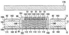
図1に示されるように、本実施形態の部品内蔵配線基板(以下「配線基板」という)10は、ICチップ搭載用の配線基板である。配線基板10は、略矩形板状のコア基板11と、コア基板11のコア主面12(図1では上面)上に形成される主面側ビルドアップ層31(主面側配線積層部)と、コア基板11のコア裏面13(図1では下面)上に形成される裏面側ビルドアップ層32(裏面側配線積層部)とからなる。
As shown in FIG. 1, a component built-in wiring board (hereinafter referred to as “wiring board”) 10 of this embodiment is a wiring board for mounting an IC chip. The
コア基板11のコア主面12上に形成された主面側ビルドアップ層31は、熱硬化性樹脂(エポキシ樹脂)からなる2層の主面側樹脂絶縁層33,35(いわゆる主面側層間絶縁層)と、銅からなる主面側導体層41とを交互に積層した構造を有している。第2層の主面側樹脂絶縁層35の表面上における複数箇所には、端子パッド44がアレイ状に形成されている。さらに、主面側樹脂絶縁層35の表面は、ソルダーレジスト37によってほぼ全体的に覆われている。ソルダーレジスト37の所定箇所には、端子パッド44を露出させる開口部46が形成されている。端子パッド44の表面上には、複数のはんだバンプ45が配設されている。各はんだバンプ45は、矩形平板状をなすICチップ21(半導体集積回路素子)の面接続端子22に電気的に接続されている。なお、各端子パッド44及び各はんだバンプ45からなる領域は、ICチップ21を搭載可能なICチップ搭載領域23(半導体集積回路素子搭載領域)である。ICチップ搭載領域23は、主面側ビルドアップ層31の表面39に設定されている。また、第2層の主面側樹脂絶縁層35内における複数箇所にはビア導体43が形成されている。各ビア導体43の下端となる箇所は、主面側樹脂絶縁層33の表面上に形成された主面側導体層41に接続されており、各ビア導体43の上端となる箇所は、主面側樹脂絶縁層35の表面上に形成された主面側導体層41、または、端子パッド44に接続されている。このビア導体43は、主面側導体層41及び端子パッド44を相互に電気的に接続している。
The main surface
図1に示されるように、コア基板11のコア裏面13上に形成された裏面側ビルドアップ層32は、上述した主面側ビルドアップ層31とほぼ同じ構造を有している。即ち、裏面側ビルドアップ層32は、熱硬化性樹脂(エポキシ樹脂)からなる2層の裏面側樹脂絶縁層34,36(いわゆる裏面側層間絶縁層)と、裏面側導体層42とを交互に積層した構造を有している。第1層の裏面側樹脂絶縁層34内における複数箇所にはビア導体47が形成されている。各ビア導体47の下端となる箇所は、裏面側樹脂絶縁層34の表面上に形成された裏面側導体層42に接続されている。第2層の裏面側樹脂絶縁層36内における複数箇所にはビア導体43が形成されており、裏面側樹脂絶縁層36の下面上において各ビア導体43の下端となる箇所には、ビア導体43を介して裏面側導体層42に電気的に接続されるBGA用パッド48が格子状に形成されている。また、裏面側樹脂絶縁層36の下面は、ソルダーレジスト38によってほぼ全体的に覆われている。ソルダーレジスト38の所定箇所には、BGA用パッド48を露出させる開口部40が形成されている。BGA用パッド48の表面上には、図示しないマザーボード(母基板)に対して電気的に接続可能な複数のはんだバンプ49が配設されている。即ち、BGA用パッド48及びはんだバンプ49は、裏面側ビルドアップ層32の表面に形成された接続端子部50を構成している。そして、各はんだバンプ49により、図1に示される配線基板10は図示しないマザーボード上に実装される。
As shown in FIG. 1, the back surface
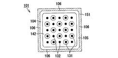
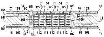
図1に示されるように、本実施形態のコア基板11は、縦25mm×横25mm×厚さ1.0mmの平面視略矩形板状である。コア基板11は、ガラスエポキシからなる基材161と、基材161の上面及び下面に形成され、シリカフィラーなどの無機フィラーを添加したエポキシ樹脂からなるサブ基材164と、同じく基材161の上面及び下面に形成され、銅からなる導体層163とによって構成されている。また、コア基板11には、複数のスルーホール導体16がコア主面12、コア裏面13及び導体層163を貫通するように形成されている。かかるスルーホール導体16は、コア基板11のコア主面12側とコア裏面13側とを接続導通するとともに、導体層163に電気的に接続している。なお、スルーホール導体16の内部は、例えばエポキシ樹脂などの閉塞体17で埋められている。スルーホール導体16の上端は、主面側樹脂絶縁層33の表面上にある主面側導体層41の一部に電気的に接続されており、スルーホール導体16の下端は、裏面側樹脂絶縁層34の下面上にある裏面側導体層42の一部に電気的に接続されている。
As shown in FIG. 1, the
図1に示されるように、コア基板11のコア主面12上には、銅からなるコア主面側導体層61がパターン形成されており、各コア主面側導体層61は、スルーホール導体16に電気的に接続されている。同様に、コア基板11のコア裏面13上には、銅からなるコア裏面側導体層62(導体層)がパターン形成されており、各コア裏面側導体層62は、スルーホール導体16に電気的に接続されている。コア裏面側導体層62は、コア主面側導体層61(厚さ75μm)よりも薄くなっており、本実施形態では65μmに設定されている。また、コア裏面側導体層62の表面及び頂部52の表面の算術平均粗さRaは、前記コア主面側導体層61の表面の算術平均粗さRa(本実施形態では0.5μm)よりも粗くなっており、具体的には0.8μmに設定されている。
As shown in FIG. 1, a core main surface
図1に示されるように、コア基板11は、コア主面12の中央部及びコア裏面13の中央部にて開口する平面視で矩形状の収容穴部90を1つ有している。即ち、収容穴部90は貫通穴である。そして、収容穴部90内には、図2〜図4等に示すセラミックコンデンサ101(部品)が、埋め込まれた状態で収容されている。なお、セラミックコンデンサ101は、コンデンサ裏面103をコア基板11のコア裏面13と同じ側に向けた状態で収容されている。本実施形態のセラミックコンデンサ101は、縦10.0mm×横10.0mm×厚さ0.8mmの平面視略矩形板状である。即ち、セラミックコンデンサ101はコア基板11よりも薄く形成されている。セラミックコンデンサ101は、コア基板11において前記ICチップ搭載領域23の真下の領域に配置されている。なお、ICチップ搭載領域23の面積(ICチップ21において面接続端子22が形成される面の面積)は、セラミックコンデンサ101のコンデンサ主面102の面積よりも小さくなるように設定されている。セラミックコンデンサ101の厚さ方向から見た場合、ICチップ搭載領域23は、セラミックコンデンサ101のコンデンサ主面102内に位置している。
As shown in FIG. 1, the
図1〜図4等に示されるように、本実施形態のセラミックコンデンサ101は、いわゆるビアアレイタイプのコンデンサである。セラミックコンデンサ101を構成するセラミック焼結体104(部品本体)は、部品主面である1つのコンデンサ主面102(図1では上面)、部品裏面である1つのコンデンサ裏面103(図1では下面)、及び、部品側面である4つのコンデンサ側面106(図1では左面、右面)を有する板状物である。
As shown in FIGS. 1 to 4 and the like, the
図2に示されるように、セラミック焼結体104は、セラミック誘電体層105を介して電源用内部電極層141とグランド用内部電極層142とを交互に積層配置した構造を有している。また、セラミック誘電体層105は、高誘電率セラミックの一種であるチタン酸バリウムの焼結体からなり、電源用内部電極層141及びグランド用内部電極層142間の誘電体(絶縁体)として機能する。電源用内部電極層141及びグランド用内部電極層142は、いずれもニッケルを主成分として形成された層であって、セラミック焼結体104の内部において一層おきに配置されている。
As shown in FIG. 2, the ceramic
図1〜図4に示されるように、セラミック焼結体104には、多数のビアホール130が形成されている。これらのビアホール130は、セラミック焼結体104をその厚さ方向に貫通するとともに、セラミック焼結体104の全面にわたって格子状(アレイ状)に配置されている。各ビアホール130内には、セラミック焼結体104のコンデンサ主面102及びコンデンサ裏面103間を連通する複数のコンデンサ内ビア導体131,132が、ニッケルを主材料として形成されている。なお本実施形態において、ビアホール130の直径は約100μmに設定されているため、コンデンサ内ビア導体131,132の直径も約100μmに設定されている。各電源用コンデンサ内ビア導体131は、各電源用内部電極層141を貫通しており、それら同士を互いに電気的に接続している。各グランド用コンデンサ内ビア導体132は、各グランド用内部電極層142を貫通しており、それら同士を互いに電気的に接続している。各電源用コンデンサ内ビア導体131及び各グランド用コンデンサ内ビア導体132は、全体としてアレイ状に配置されている。本実施形態では、説明の便宜上、コンデンサ内ビア導体131,132を5列×5列で図示したが、実際にはさらに多くの列が存在している。
As shown in FIGS. 1 to 4, a large number of via
そして図2等に示されるように、セラミック焼結体104のコンデンサ主面102上には、複数の主面側電源用電極111と複数の主面側グランド用電極112とが突設されている。なお、各主面側グランド用電極112は、コンデンサ主面102上において個別に形成されているが、一体に形成されていてもよい。主面側電源用電極111は、複数の電源用コンデンサ内ビア導体131におけるコンデンサ主面102側の端面に対して直接接続されており、主面側グランド用電極112は、複数のグランド用コンデンサ内ビア導体132におけるコンデンサ主面102側の端面に対して直接接続されている。
As shown in FIG. 2 and the like, a plurality of main surface side
また、セラミック焼結体104のコンデンサ裏面103上には、複数の裏面側電源用電極121(表面電極)と複数の裏面側グランド用電極122(表面電極)とが突設されている。なお、各裏面側グランド用電極122は、コンデンサ裏面103上において個別に形成されているが、一体に形成されていてもよい。裏面側電源用電極121は、複数の電源用コンデンサ内ビア導体131におけるコンデンサ裏面103側の端面に対して直接接続されており、裏面側グランド用電極122は、複数のグランド用コンデンサ内ビア導体132におけるコンデンサ裏面103側の端面に対して直接接続されている。よって、電源用電極111,121は電源用コンデンサ内ビア導体131及び電源用内部電極層141に導通しており、グランド用電極112,122はグランド用コンデンサ内ビア導体132及びグランド用内部電極層142に導通している。
Further, on the capacitor back
図2等に示されるように、電極111,112,121,122は、ニッケルを主材料として形成され、表面が図示しない銅めっき層によって全体的に被覆されている。なお本実施形態の電極111,112,121,122は、直径が約500μm、厚さが約50μmの平面視略矩形状をなし、ピッチの最小長さが約580μmに設定されている。
As shown in FIG. 2 and the like, the
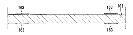
図1,図2に示されるように、各裏面側電源用電極121上及び各裏面側グランド用電極122上には、それぞれ突設導体51が突設されている。本実施形態の突設導体51は、銅めっきによって形成された導体(銅ポスト)である。また、各突設導体51は、断面円形状かつ断面等面積の円柱状をなしており、各突設導体51の中心軸線は、電極121,122の中心と一致している。各突設導体51の頂部52の表面は、円形状をなしており、頂部52の表面は前記コンデンサ主面102と平行になっている。また、各突設導体51の直径は、電極121,122の直径と等しく、かつ、コンデンサ内ビア導体131,132の直径(約100μm)よりも大きくなっており、本実施形態では約500μmに設定されている。また、配線基板10が完成した状態での各突設導体51の厚さは、本実施形態では100μmに設定されている。即ち、各突設導体51の厚さは、電極121,122の厚さよりも大きくなっている。また、各突設導体51の頂部52の表面は、前記コア裏面側導体層62の表面と同一平面上に位置している。そして、各突設導体51は、最もコア裏面13側に位置する前記裏面側樹脂絶縁層34内における複数箇所に形成されたビア導体47に接続されている。なお本実施形態では、裏面側樹脂絶縁層34の厚さが約50μmに設定され、厚さのバラツキが5μmに設定されている。
As shown in FIGS. 1 and 2, projecting
図1〜図4等に示されるように、前記セラミック焼結体104は樹脂被覆層151によって覆われている。樹脂被覆層151は、1つのコンデンサ主面102と、1つの前記コンデンサ裏面103と、4つの前記コンデンサ側面106全体とを覆っている。セラミックコンデンサ101が配線基板10に内蔵された状態において、コンデンサ主面102を覆う樹脂被覆層151は、コンデンサ主面102を完全に覆っておらず、電極111,112が露出した状態になっている。同様に、コンデンサ裏面103を覆う樹脂被覆層151は、コンデンサ裏面103を完全に覆っておらず、電極121,122上に突設された突設導体51の頂部52の表面が露出した状態になっている。なお、コンデンサ主面102を覆う樹脂被覆層151の厚さは50μmに設定され、コンデンサ裏面103を覆う樹脂被覆層151の厚さは150μmに設定され、コンデンサ側面106を覆う樹脂被覆層151の厚さは1000μmに設定されている。即ち、コンデンサ裏面103を覆う樹脂被覆層151の厚さは、各突設導体51の厚さよりも大きくなっており、各突設導体51の頂部52の表面は、樹脂被覆層151によって覆われている。また、樹脂被覆層151は、樹脂絶縁層33〜36と同じ材料(即ち、熱硬化性樹脂であるエポキシ樹脂)によって形成されている。これにより、樹脂被覆層151の熱膨張係数も、樹脂絶縁層33〜36の熱膨張係数と同じ値となっており、具体的には、10〜60ppm/℃程度(具体的には20ppm/℃程度)に設定されている。また、樹脂被覆層151の熱膨張係数は、セラミック焼結体104の熱膨張係数よりも大きい値に設定されている。
As shown in FIGS. 1 to 4 and the like, the ceramic
図1等に示されるように、前記収容穴部90の内壁面91と、セラミックコンデンサ101のコンデンサ側面106を覆う樹脂被覆層151の表面との隙間は、前記コア裏面13上及びコンデンサ裏面103上に形成された樹脂層92の一部によって埋められている。この樹脂層92は、セラミックコンデンサ101をコア基板11に固定する機能を有している。樹脂層92は、樹脂絶縁層33〜36及び樹脂被覆層151と同じ材料(即ち、熱硬化性樹脂であるエポキシ樹脂)によって形成されている。これにより、樹脂層92の熱膨張係数も、樹脂絶縁層33〜36及び樹脂被覆層151の熱膨張係数と同じ値となっており、具体的には、10〜60ppm/℃程度(具体的には20ppm/℃程度)に設定されている。なお、セラミックコンデンサ101は、平面視略正方形状をなしており、四隅に面取り寸法0.55mm以上(本実施形態では面取り寸法0.6mm)の面取り部を有している。これにより、温度変化に伴う樹脂層92の変形時において、セラミックコンデンサ101の角部への応力集中を緩和できるため、樹脂層92のクラックの発生を防止できる。
As shown in FIG. 1 and the like, the gap between the
そして図1に示されるように、コンデンサ主面102側にある電極111,112は、ビア導体47、主面側導体層41、ビア導体43、端子パッド44、はんだバンプ45及びICチップ21の面接続端子22を介して、ICチップ21に電気的に接続される。一方、コンデンサ裏面103側にある電極121,122は、突設導体51、ビア導体47、裏面側導体層42、ビア導体43、BGA用パッド48及びはんだバンプ49を介して、図示しないマザーボードが有する電極に対して電気的に接続される。
As shown in FIG. 1, the
例えば、マザーボード側から電極121,122を介して通電を行い、電源用内部電極層141−グランド用内部電極層142間に電圧を加えると、電源用内部電極層141に例えばプラスの電荷が蓄積し、グランド用内部電極層142に例えばマイナスの電荷が蓄積する。その結果、セラミックコンデンサ101がコンデンサとして機能する。また、セラミックコンデンサ101では、電源用コンデンサ内ビア導体131及びグランド用コンデンサ内ビア導体132がそれぞれ交互に隣接して配置され、かつ、電源用コンデンサ内ビア導体131及びグランド用コンデンサ内ビア導体132を流れる電流の方向が互いに逆向きになるように設定されている。これにより、インダクタンス成分の低減化が図られている。
For example, when energization is performed from the motherboard side via the
次に、本実施形態の配線基板10の製造方法について述べる。
Next, a method for manufacturing the
コア基板準備工程では、コア基板11の中間製品を従来周知の手法により作製し、あらかじめ準備しておく。
In the core substrate preparation step, an intermediate product of the
コア基板11の中間製品は以下のように作製される。まず、縦350mm×横375mm×厚み0.6mmの基材161の両面に銅箔162が貼付された銅張積層板(図5参照)を準備する。次に、銅張積層板の両面の銅箔162のエッチングを行って導体層163を例えばサブトラクティブ法によってパターニングする(図6参照)。具体的には、無電解銅めっきの後、この無電解銅めっき層を共通電極として電解銅めっきを施す。さらにドライフィルムをラミネートし、同ドライフィルムに対して露光及び現像を行うことにより、ドライフィルムを所定パターンに形成する。この状態で、不要な電解銅めっき層、無電解銅めっき層及び銅箔162をエッチングで除去する。その後、ドライフィルムを剥離する。次に、基材161の上面及び下面と導体層163とを粗化した後、基材161の上面及び下面に、無機フィラーが添加されたエポキシ樹脂フィルム(厚さ80μm)を熱圧着により貼付し、サブ基材164を形成する(図7参照)。
The intermediate product of the
次に、上側のサブ基材164の上面にコア裏面側導体層62(厚さ75μm)をパターン形成するとともに、下側のサブ基材164の下面にコア主面側導体層61(厚さ50μm)をパターン形成する。具体的には、上側のサブ基材164の上面及び下側のサブ基材164の下面に対する無電解銅めっきを行った後にエッチングレジストを形成し、次いで電解銅めっきを行う。さらに、エッチングレジストを除去してソフトエッチングを行う。次に、基材161及びサブ基材164からなる積層体に対してルータを用いて孔あけ加工を行い、収容穴部90となる貫通孔を所定位置に形成し、コア基板11の中間製品を得る(図8参照)。なお、コア基板11の中間製品とは、コア基板11となるべき領域を平面方向に沿って縦横に複数配列した構造の多数個取り用コア基板である。
Next, the core back surface side conductor layer 62 (thickness 75 μm) is patterned on the upper surface of the upper
また、部品準備工程(コンデンサ準備工程)では、突設導体51を有するセラミックコンデンサ101を従来周知の手法により作製し、あらかじめ準備しておく。
In the component preparation step (capacitor preparation step), the
セラミックコンデンサ101は以下のように作製される。即ち、セラミックのグリーンシートを形成し、このグリーンシートに内部電極層用ニッケルペーストをスクリーン印刷して乾燥させる。これにより、後に電源用内部電極層141となる電源用内部電極部と、グランド用内部電極層142となるグランド用内部電極部とが形成される。次に、電源用内部電極部が形成されたグリーンシートとグランド用内部電極部が形成されたグリーンシートとを交互に積層し、シート積層方向に押圧力を付与することにより、各グリーンシートを一体化してグリーンシート積層体を形成する。
The
さらに、レーザー加工機を用いてグリーンシート積層体にビアホール130を多数個貫通形成し、図示しないペースト圧入充填装置を用いて、ビア導体用ニッケルペーストを各ビアホール130内に充填する。次に、グリーンシート積層体の上面上にペーストを印刷し、グリーンシート積層体の上面側にて各導体部の上端面を覆うように裏面側電源用電極121及び裏面側グランド用電極122を形成する。また、グリーンシート積層体の下面上にペーストを印刷し、グリーンシート積層体の下面側にて各導体部の下端面を覆うように主面側電源用電極111及び主面側グランド用電極112を形成する。
Further, a number of via
この後、グリーンシート積層体の乾燥を行い、各電極111,112,121,122をある程度固化させる。次に、グリーンシート積層体を脱脂し、さらに所定温度で所定時間焼成を行う。その結果、チタン酸バリウム及びペースト中のニッケルが同時焼結し、セラミック焼結体104となる。
Thereafter, the green sheet laminate is dried to solidify the
次に、得られたセラミック焼結体104が有する各電極111,112,121,122に対して無電解銅めっき(厚さ10μm程度)を行う。その結果、各電極111,112,121,122の上に銅めっき層が形成される。
Next, electroless copper plating (thickness of about 10 μm) is performed on each
次に、セラミック焼結体104のコンデンサ裏面103上にドライフィルム153をラミネートし、同ドライフィルム153に対して露光及び現像を行うことにより、電極121,122の表面全体を露出させる複数の開口部152をドライフィルム153に形成する(図9参照)。これらの開口部152は、突設導体51の形成予定位置に存在している。そして、ドライフィルム153を介して開口部152の内面に対する電解銅めっきを行う(図10参照)。さらに、ドライフィルム153を除去する。その結果、裏面側電源用電極121上及び裏面側グランド用電極122上にそれぞれ突設導体51が形成され、セラミックコンデンサ101が完成する(図11参照)。なお、この時点での各突設導体51の厚さは、190μm程度に設定されており、前記収容穴部90内にセラミックコンデンサ101が収容された状態(図15〜図17参照)でコア裏面13から突出する程度の厚さに形成されている。なお、本実施形態において各突設導体51の厚さとして設定した「190μm程度」という値は、コア基板11の厚さバラツキとセラミックコンデンサ101の厚さバラツキとを吸収するのに最低限必要な厚さである。そして、この程度の厚さに設定することにより、後述する高さ合わせ工程での表面研磨量を最小限に抑えることができ、生産性の低下を未然に防止することができる。
Next, by laminating a
そして、完成したセラミックコンデンサ101のコンデンサ裏面103側を粗化した後、マウント装置(ヤマハ発動機株式会社製)を用いて、複数のセラミックコンデンサ101を、コンデンサ裏面103を上にした状態で治具(図示略)にセットする。詳述すると、治具上には剥離可能な粘着テープ172が配置されており、各セラミックコンデンサ101は、粘着テープ172の粘着面に貼り付けられて仮固定されている(図12参照)。また、粘着テープ172上には矩形枠状のフレーム175が貼り付けられており、フレーム175内には各セラミックコンデンサ101が配置されている。このとき、各セラミックコンデンサ101は、粘着テープ172の粘着面と平行に配置した状態で、粘着面に沿って互いに離間配置されている。
Then, after roughening the capacitor back
続く樹脂被覆層形成工程では、治具にセットされた各セラミックコンデンサ101に、未硬化状態の樹脂被覆層151であるエポキシ樹脂フィルム173(厚さ400μm)をラミネートする(図13,図14参照)。このとき、エポキシ樹脂フィルム173の一部は、互いに隣接するセラミックコンデンサ101のコンデンサ側面106間、及び、コンデンサ側面106とフレーム175の内壁面との間に充填される。そして、加熱処理(キュアなど)を行ってエポキシ樹脂フィルム173を硬化させる。このとき、硬化状態の樹脂被覆層151(樹脂材)の一部が、各突設導体51間に配置された状態となる。なお、この状態のものは、樹脂被覆層151を有するセラミックコンデンサ101となるべき製品領域を平面方向に沿って縦横に複数配列した配線基板内蔵用コンデンサ集合体174であると把握することができる。次に、従来周知のブレード装置を用いることにより、製品領域の外形線(図14の一点鎖線参照)に沿って配線基板内蔵用コンデンサ集合体174の表面及び裏面にブレーク溝を形成する。さらに、配線基板内蔵用コンデンサ集合体174を、ブレーク溝に沿って分割して個片化する。その際、各コンデンサ側面106にそれぞれ厚さ500μmの樹脂被覆層151が形成されるように切断する。その結果、コンデンサ主面102、コンデンサ裏面103及びコンデンサ側面106が樹脂被覆層151によって覆われるセラミックコンデンサ101が多数個同時に得られる。そして、この時点で、粘着テープ172を剥離する。
In the subsequent resin coating layer forming step, an epoxy resin film 173 (thickness 400 μm) which is an uncured
続く収容工程では、マウント装置(ヤマハ発動機株式会社製)を用いて、コア裏面13とコンデンサ裏面103とを同じ側に向けた状態で収容穴部90内にセラミックコンデンサ101を収容する(図15参照)。この状態において、各突設導体51の頂部52の表面は、コア裏面側導体層62の表面よりも上方に位置している。なお、収容穴部90のコア主面12側開口は、剥離可能な粘着テープ171でシールされている。この粘着テープ171は、支持台(図示略)によって支持されている。かかる粘着テープ171の粘着面には、セラミックコンデンサ101が貼り付けられて仮固定されている。また、セラミックコンデンサ101がコア基板11よりも薄いことから、コア裏面13とコンデンサ裏面103との間には段差が生じている。
In the subsequent housing process, the
続く樹脂層形成工程では、コア裏面13上及びコンデンサ裏面103上に、未硬化状態の樹脂層92である樹脂シート176(厚さ200μm)をラミネートする(図16,図17参照)。併せて、樹脂層92(樹脂シート176)の一部で、収容穴部90の内壁面91とコンデンサ側面106を覆う樹脂被覆層151の表面との隙間を埋める。続く固定工程では、加熱処理(キュアなど)を行って樹脂層92(樹脂シート176)を硬化させ、セラミックコンデンサ101をコア基板11に固定する。
In the subsequent resin layer forming step, a resin sheet 176 (thickness: 200 μm), which is an
続く高さ合わせ工程では、各突設導体51の頂部52の表面と、コア裏面側導体層62の表面とを同じ高さに合わせる(図18参照)。具体的に言うと、ベルトサンダー装置を用いて、コア裏面側導体層62の表面よりも上方に位置している頂部52の表面を研磨して各突設導体51を低くすると同時に、樹脂層92と、コンデンサ裏面103を覆う樹脂被覆層151とを研磨する。さらに、樹脂層92の研磨に伴って露出したコア裏面側導体層62の表面も研磨する。その結果、頂部52の一部及びコア裏面側導体層62の一部が機械的に除去され、各突設導体51の厚さが100μmとなり、コア裏面側導体層62の厚さが65μmとなる。なお、ベルトサンダー装置に取り付けられたサンドペーパーの研磨面の算術平均粗さRaは、コア裏面側導体層62の表面及び頂部52の表面の研磨後における算術平均粗さRaと等しくなっており、具体的には0.8μmに設定されている。また、ベルトサンダー装置による研磨時間は、30秒に設定されている。そして、この時点で、粘着テープ171を剥離する。なお、電極111,112の表面及びコア主面側導体層61の表面は、粘着テープ171に接触しているために、研磨しなくても同じ高さに位置している。
In the subsequent height adjusting step, the surface of the
次に、従来周知の手法に基づいてコア主面12の上に主面側ビルドアップ層31を形成するとともに、コア裏面13の上に裏面側ビルドアップ層32を形成する。具体的に言うと、まず、コア主面12及びコンデンサ主面102上に感光性エポキシ樹脂を被着して露光及び現像を行うことにより、最下層の主面側樹脂絶縁層33を形成する(図19参照)。なお、感光性エポキシ樹脂を被着する代わりに、絶縁樹脂や液晶ポリマー(LCP:Liquid Crystalline Polymer)を被着してもよい。
Next, the main surface
次に、裏面側層間絶縁層形成工程を実施し、コア裏面13及びコンデンサ裏面103に感光性エポキシ樹脂を被着し、露光及び現像を行うことにより、裏面側樹脂絶縁層34を形成する(図19参照)。なお、感光性エポキシ樹脂を被着する代わりに、絶縁樹脂や液晶ポリマーを被着してもよい。さらに、YAGレーザーまたは炭酸ガスレーザーを用いてレーザー孔あけ加工を行い、ビア導体47が形成されるべき位置にビア孔181,182を形成する(図20参照)。具体的には、主面側樹脂絶縁層33を貫通するビア孔181を形成し、主面側電源用電極111及び主面側グランド用電極112を露出させる。また、裏面側樹脂絶縁層34を貫通するビア孔182を形成し、裏面側電源用電極121上に突設された突設導体51の頂部52の表面と、裏面側グランド用電極122上に突設された突設導体51の頂部52の表面とを露出させる(ビア孔形成工程)。
Next, a back surface side interlayer insulating layer forming step is performed, a photosensitive epoxy resin is applied to the core back
さらに、ドリル機を用いて孔あけ加工を行い、コア基板11及び樹脂絶縁層33,34を貫通する貫通孔191を所定位置にあらかじめ形成しておく(図20参照)。そして、樹脂絶縁層33,34の表面上、ビア孔181,182の内面、及び、貫通孔191の内面に対する無電解銅めっきを行った後にエッチングレジストを形成し、次いで電解銅めっきを行う。さらに、エッチングレジストを除去してソフトエッチングを行う。これにより、主面側樹脂絶縁層33上に主面側導体層41が形成されるとともに、裏面側樹脂絶縁層34上に裏面側導体層42がパターン形成される(図21参照)。これと同時に、貫通孔191内にスルーホール導体16が形成されるとともに、各ビア孔181,182の内部にビア導体47が形成される(ビア導体形成工程)。その後、スルーホール導体16の空洞部を絶縁樹脂材料(エポキシ樹脂)で穴埋めし、閉塞体17を形成する(図22参照)。
Further, drilling is performed using a drill machine, and a through
次に、樹脂絶縁層33,34上に感光性エポキシ樹脂を被着し、露光及び現像を行うことにより、ビア導体43が形成されるべき位置にビア孔183,184を有する樹脂絶縁層35,36を形成する(図22参照)。なお、感光性エポキシ樹脂を被着する代わりに、絶縁樹脂や液晶ポリマーを被着してもよい。この場合、レーザー加工機などにより、ビア導体43が形成されるべき位置にビア孔183,184が形成される。次に、従来公知の手法に従って電解銅めっきを行い、前記ビア孔183,184の内部にビア導体43を形成するとともに、主面側樹脂絶縁層35上に端子パッド44を形成し、裏面側樹脂絶縁層36上にBGA用パッド48を形成する。
Next, a photosensitive epoxy resin is deposited on the resin insulation layers 33, 34, and exposure and development are performed, whereby the resin insulation layers 35, 184 having via
次に、樹脂絶縁層35,36上に感光性エポキシ樹脂を塗布して硬化させることにより、ソルダーレジスト37,38を形成する。次に、所定のマスクを配置した状態で露光及び現像を行い、ソルダーレジスト37,38に開口部40,46をパターニングする。さらに、端子パッド44上にはんだバンプ45を形成し、かつ、BGA用パッド48上にはんだバンプ49を形成する。なお、この状態のものは、配線基板10となるべき製品領域を平面方向に沿って縦横に複数配列した多数個取り用配線基板であると把握することができる。さらに、多数個取り用配線基板を分割すると、個々の製品である配線基板10が多数個同時に得られる。
Next, solder resists 37 and 38 are formed by applying and curing a photosensitive epoxy resin on the
従って、本実施形態によれば以下の効果を得ることができる。 Therefore, according to the present embodiment, the following effects can be obtained.
(1)本実施形態の配線基板10の製造方法によれば、高さ合わせ工程を行って、複数の突設導体51の頂部52の表面と、コア裏面13上に形成されたコア裏面側導体層62の表面とを同じ高さに合わせているため、厚さのバラツキの小さい裏面側樹脂絶縁層34を形成することができる。よって、ビア孔形成工程において裏面側樹脂絶縁層34を貫通するビア孔182を複数形成し、ビア導体形成工程において各ビア孔182内にビア導体47を形成したとしても、ビア孔182の深さのバラツキが小さくなる。これにより、裏面側樹脂絶縁層34に対するレーザー孔あけ加工を行うにあたり、レーザーの出力を一定に調節することができるため、各ビア孔182を容易かつ確実に貫通させることができる。しかも、各ビア孔182内にビア導体47を確実に形成することができる。その結果、突設導体51とビア導体47とを確実に導通させることができるため、不良品の発生を防止でき、信頼性に優れた配線基板10を得ることができる。
(1) According to the manufacturing method of the
(2)本実施形態では、高さ合わせ工程において、コンデンサ裏面103を覆う樹脂被覆層151を各突設導体51間に配置した状態で、頂部52の表面を研磨している。これにより、各突設導体51が樹脂被覆層151によって固定されるため、高さ合わせ工程を行う際に各突設導体51に大きな力がかかったとしても、各突設導体51の破損を防止することができる。また、樹脂被覆層151を各突設導体51間に配置することにより、各突設導体51間の凹部が埋められて平坦になるため、頂部52の表面や樹脂被覆層151の研磨時に生じる粉が残りにくくなる。
(2) In the present embodiment, the surface of the
(3)本実施形態では、樹脂層92の形成によってコア基板11のコア裏面13側が平坦になるため、コア裏面13上に裏面側ビルドアップ層32を形成すると、裏面側ビルドアップ層32の表面に形成される接続端子部50(即ちBGA用パッド48)の高さが揃うようになる。従って、配線基板10を確実にマザーボード上に実装することができ、配線基板10の信頼性が向上する。
(3) In this embodiment, since the core back
(4)本実施形態では、高さ合わせ工程において、突設導体51の頂部52及びコア裏面側導体層62の両方を除去している。これにより、頂部52の表面の平坦化が図られるだけでなく、樹脂層92から露出したコア裏面側導体層62の表面の平坦化も図られるため、突設導体51やコア裏面側導体層62の上側に形成される裏面側樹脂絶縁層34の厚さのバラツキがよりいっそう小さくなる。よって、裏面側樹脂絶縁層34にビア孔182を複数形成した際に、ビア孔182の深さのバラツキがよりいっそう小さくなるため、各ビア孔182内にビア導体47をより確実に形成させることができ、突設導体51とビア導体47とをより確実に導通させることができる。その結果、よりいっそう信頼性に優れた配線基板10を得ることができる。
(4) In the present embodiment, both the
(5)本実施形態では、セラミックコンデンサ101がICチップ搭載領域23に搭載されたICチップ21の直下に配置されるため、セラミックコンデンサ101とICチップ21とをつなぐ配線が短くなり、配線のインダクタンス成分の増加が防止される。従って、セラミックコンデンサ101によるICチップ21のスイッチングノイズを確実に低減できるとともに、電源電圧の確実な安定化を図ることができる。また、ICチップ21とセラミックコンデンサ101との間で侵入するノイズを極めて小さく抑えることができるため、誤動作等の不具合を生じることもなく高い信頼性を得ることができる。
(5) In this embodiment, since the
(6)本実施形態では、ICチップ搭載領域23がセラミックコンデンサ101の真上の領域内に位置しているため、ICチップ搭載領域23に搭載されるICチップ21は高剛性で熱膨張率が小さいセラミックコンデンサ101によって支持される。よって、上記ICチップ搭載領域23においては、主面側ビルドアップ層31が変形しにくくなるため、ICチップ搭載領域23に搭載されるICチップ21をより安定的に支持できる。従って、大きな熱応力に起因するICチップ21のクラックや接続不良を防止することができる。ゆえに、10mm角以上の大型のICチップや、脆いとされるLow−k(低誘電率)のICチップを用いることができる。
(6) In this embodiment, since the IC
なお、本実施形態は以下のように変更してもよい。 In addition, you may change this embodiment as follows.
・上記実施形態の突設導体51は、銅めっきによって形成された導体(同ポスト)であったが、例えば、銅ペーストを印刷することによって形成された導体であってもよい。
The protruding
・上記実施形態では、セラミック焼結体104のコンデンサ裏面103上に配置された電極121,122上に、突設導体51が突設されていた。しかし、コンデンサ主面102上に配置された電極111,112上にも、突設導体51が突設されていてもよい。このようにすれば、電極121,122及び裏面側樹脂絶縁層34内のビア導体47を、突設導体51を介して確実に接続できるだけでなく、電極111,112及び主面側樹脂絶縁層33内のビア導体47も、突設導体51を介して確実に接続できるため、よりいっそう信頼性に優れた配線基板10を得ることができる。しかし、コスト低減の観点から言えば、コア主面側導体層61と同じ高さにある電極111,112上に突設導体51を突設するよりも、電極121,122上のみに突設導体51を突設することが好ましい。
In the above embodiment, the protruding
・上記実施形態では、セラミックコンデンサ101に樹脂被覆層151を形成する樹脂被覆層形成工程が行われるとともに、コア裏面13上及びコンデンサ裏面103上に樹脂層92を形成する樹脂層形成工程が行われていたが、樹脂被覆層形成工程及び樹脂層形成工程のいずれか一方を省略してもよい。樹脂被覆層形成工程を省略した場合、高さ合わせ工程では、硬化状態の樹脂層92を各突設導体51間に配置した状態で、頂部52の表面を研磨する。なお、樹脂層形成工程を省略した場合、コンデンサ側面106を覆う樹脂被覆層151は、上記実施形態の場合よりも厚く(例えば900μm程度)形成されることがよい。
In the above embodiment, the resin coating layer forming step for forming the
・上記実施形態では、主面側ビルドアップ層31とは別に設けられた樹脂層92の一部によって、収容穴部90の内壁面91とコンデンサ側面106を覆う樹脂被覆層151の表面との隙間を埋めていた。しかし、主面側ビルドアップ層31を構成する裏面側樹脂絶縁層34の一部によって、収容穴部90の内壁面91とコンデンサ側面106を覆う樹脂被覆層151の表面との隙間を埋めてもよい。このようにすれば、樹脂層形成工程を行わなくても済み、配線基板10の製造に必要な工数が減るため、配線基板10を容易にかつ低コストで形成できる。
In the above embodiment, the gap between the
・上記実施形態では、主面側ビルドアップ層31側の表面39にICチップ搭載領域23を設定してそこにICチップ21を搭載する一方、裏面側ビルドアップ層32側の表面にマザーボード側と接続可能なBGAパッド48及びはんだバンプ49を形成した。これに対し、例えば、裏面側ビルドアップ層32側の表面にICチップ搭載領域23を設定してそこにICチップ21を搭載する一方、主面側ビルドアップ層31側の表面39にマザーボード側と接続可能なBGAパッド48及びはんだバンプ49を形成してもよい。この構成の場合、ICチップ搭載側に位置する電極121,122と、マザーボード接続側に位置する電極111,112とを比較すると、前者のほうが突設導体51の厚さ分だけ実質的に厚くなる。ゆえに、ICチップ21に電気的に接続するセラミックコンデンサ101の導体部分を低抵抗にすることができる。さらに、ICチップ21は主面側ビルドアップ層31側の表面39及び裏面側ビルドアップ層32側の表面の両方に搭載されることもできる。
In the above embodiment, the IC
次に、前述した実施形態によって把握される技術的思想を以下に列挙する。 Next, the technical ideas grasped by the embodiment described above are listed below.
(1)コア主面及びコア裏面を有し、少なくとも前記コア裏面にて開口する収容穴部を有するコア基板を準備するコア基板準備工程と、部品主面、部品裏面及び部品側面を有する部品本体、前記部品裏面上に配置された複数の表面電極、前記複数の表面電極上にて突設された複数の突設導体を有する部品を準備する部品準備工程と、前記コア基板準備工程及び前記部品準備工程後、前記コア裏面と前記部品裏面とを同じ側に向けた状態で、前記収容穴部内に前記部品を収容する収容工程と、前記収容工程後、前記複数の突設導体の頂部の表面と、前記コア裏面上に形成された導体層の表面とを同じ高さに合わせる高さ合わせ工程とを含むことを特徴とする部品内蔵配線基板の製造方法。 (1) A core substrate preparation step of preparing a core substrate having a core main surface and a core back surface and having an accommodation hole opening at least on the core back surface, and a component main body having a component main surface, a component back surface, and a component side surface A component preparation step of preparing a component having a plurality of surface electrodes disposed on the back surface of the component, a plurality of protruding conductors protruding on the plurality of surface electrodes, the core substrate preparation step, and the component After the preparation step, with the core back surface and the component back surface facing the same side, the housing step of housing the component in the housing hole, and the top surface of the plurality of protruding conductors after the housing step And a height adjusting step for adjusting the surface of the conductor layer formed on the back surface of the core to the same height.
(2)コア主面及びコア裏面を有し、少なくとも前記コア裏面にて開口する収容穴部を有するコア基板を準備するコア基板準備工程と、部品主面、部品裏面及び部品側面を有する部品本体、前記部品裏面上に突設された複数の突設導体を有する部品を準備する部品準備工程と、前記コア基板準備工程及び前記部品準備工程後、前記コア裏面と前記部品裏面とを同じ側に向けた状態で、前記収容穴部内に前記部品を収容する収容工程と、前記収容工程後、前記複数の突設導体の頂部の表面、及び、前記コア裏面上に形成された導体層の表面の少なくとも一方を研磨することにより、前記頂部の表面と前記導体層の表面とを同じ高さに合わせる高さ合わせ工程とを含むことを特徴とする部品内蔵配線基板の製造方法。 (2) A core substrate preparation step of preparing a core substrate having a core main surface and a core back surface and having an accommodation hole opening at least on the core back surface, and a component main body having a component main surface, a component back surface, and a component side surface A component preparing step of preparing a component having a plurality of protruding conductors protruding on the component back surface, and the core back surface and the component back surface on the same side after the core substrate preparing step and the component preparing step. A housing step of housing the component in the housing hole, and a surface of the top of the plurality of projecting conductors and a surface of the conductor layer formed on the back surface of the core after the housing step. A method for manufacturing a wiring board with a built-in component, comprising: a step of adjusting the height of the top surface and the surface of the conductor layer to the same height by polishing at least one of them.
(3)コア主面及びコア裏面を有し、少なくとも前記コア裏面にて開口する収容穴部を有するコア基板を準備するコア基板準備工程と、コンデンサ主面、コンデンサ裏面及びコンデンサ側面を有し、誘電体層を介して複数の内部電極層が積層配置された構造を有するコンデンサ本体、前記複数の内部電極層に接続される複数のコンデンサ内ビア導体、前記複数のコンデンサ内ビア導体における少なくとも前記コンデンサ裏面側の端部に接続された複数の表面電極、及び、前記複数の表面電極上に突設された複数の突設導体を備え、前記複数のコンデンサ内ビア導体が全体としてアレイ状に配置されたビアアレイタイプのコンデンサを準備するコンデンサ準備工程と、前記コア基板準備工程及び前記コンデンサ準備工程後、前記コア裏面と前記コンデンサ裏面とを同じ側に向けた状態で、前記収容穴部内に前記コンデンサを収容する収容工程と、前記収容工程後、前記複数の突設導体の頂部の表面と、前記コア裏面上に形成された導体層の表面とを同じ高さに合わせる高さ合わせ工程とを含むことを特徴とするコンデンサ内蔵配線基板の製造方法。 (3) having a core main surface and a core back surface, and having a core substrate preparation step of preparing a core substrate having an accommodation hole opening at least on the core back surface, a capacitor main surface, a capacitor back surface, and a capacitor side surface; Capacitor body having a structure in which a plurality of internal electrode layers are stacked and disposed via a dielectric layer, a plurality of via conductors in a capacitor connected to the plurality of internal electrode layers, and at least the capacitor in the plurality of via conductors in the capacitor A plurality of surface electrodes connected to the end on the back surface side, and a plurality of projecting conductors projecting from the plurality of surface electrodes, and the plurality of via conductors in the capacitor are arranged in an array as a whole. Capacitor preparation step for preparing a via array type capacitor, the core substrate preparation step and the capacitor preparation step, the core back surface and the An accommodation step of accommodating the capacitor in the accommodation hole with the back surface of the capacitor facing the same side, and after the accommodation step, formed on the top surfaces of the plurality of protruding conductors and on the core back surface And a height adjusting step for adjusting the surface of the conductor layer to the same height.
コア主面及びコア裏面を有するとともに、少なくとも前記コア裏面にて開口する収容穴部を有し、前記コア主面上にコア主面側導体層が形成されるとともに、前記コア裏面上にコア裏面側導体層が形成されるコア基板と、
部品主面、部品裏面及び部品側面を有する部品本体、前記部品裏面上に突設された複数の突設導体を有し、前記コア裏面と前記部品裏面とを同じ側に向けた状態で前記収容穴部に収容された部品と、
裏面側層間絶縁層及び裏面側導体層を前記コア裏面上にて積層した構造を有するとともに、半導体集積回路素子を搭載可能な半導体集積回路素子搭載領域が表面に設定された裏面側配線積層部と、
主面側層間絶縁層及び主面側導体層を前記コア主面上にて積層した構造を有し、母基板に接続可能な接続端子部が表面に形成された主面側配線積層部と
を備える部品内蔵配線基板であって、
前記コア裏面側導体層の表面及び前記複数の突設導体の頂部の表面が同一平面上に位置するとともに、前記コア裏面側導体層の表面及び前記頂部の表面の算術平均粗さが、前記コア主面側導体層の表面の算術平均粗さよりも粗くなっており、
前記コア裏面側導体層は、前記コア主面側導体層よりも薄くなっている
ことを特徴とする部品内蔵配線基板。
The core has a core main surface and a core back surface, and has a receiving hole that opens at least in the core back surface. A core main surface side conductor layer is formed on the core main surface, and the core back surface on the core back surface. A core substrate on which a side conductor layer is formed;
A component main body having a component main surface, a component back surface, and a component side surface, a plurality of projecting conductors projecting on the component back surface, and the housing with the core back surface and the component back surface facing the same side Parts housed in holes,
A back surface side wiring laminated portion having a structure in which a back surface side interlayer insulating layer and a back surface side conductor layer are stacked on the back surface of the core, and a semiconductor integrated circuit element mounting region on which a semiconductor integrated circuit element can be mounted is set on the surface; ,
A main surface side wiring laminated portion having a structure in which a main surface side interlayer insulating layer and a main surface side conductor layer are laminated on the core main surface, and a connection terminal portion connectable to a mother board is formed on the surface. A component built-in wiring board comprising:
The surface of the core back surface side conductor layer and the top surface of the plurality of protruding conductors are located on the same plane, and the arithmetic average roughness of the surface of the core back surface side conductor layer and the surface of the top portion is the core. It is rougher than the arithmetic average roughness of the surface of the main surface side conductor layer,
The component built-in wiring board, wherein the core back surface side conductor layer is thinner than the core main surface side conductor layer.
10…部品内蔵配線基板(配線基板)
11…コア基板
12…コア主面
13…コア裏面
21…半導体集積回路素子としてのICチップ
23…半導体集積回路素子搭載領域としてのICチップ搭載領域
31…主面側配線積層部としての主面側ビルドアップ層
32…裏面側配線積層部としての裏面側ビルドアップ層
33,35…主面側層間絶縁層としての主面側樹脂絶縁層
34,36…裏面側層間絶縁層としての裏面側樹脂絶縁層
39…主面側配線積層部の表面
41…主面側導体層
42…裏面側導体層
47…ビア導体
50…接続端子部
51…突設導体
52…頂部
61…コア主面側導体層
62…コア裏面上に形成された導体層としてのコア裏面側導体層
90…収容穴部
91…内壁面
92…樹脂層
101…部品としてのセラミックコンデンサ
102…部品主面としてのコンデンサ主面
103…部品裏面としてのコンデンサ裏面
104…部品本体としてのセラミック焼結体
106…部品側面としてのコンデンサ側面
121…表面電極としての裏面側電源用電極
122…表面電極としての裏面側グランド用電極
151…樹脂材としての樹脂被覆層
182…ビア孔
10 ... Wiring board with built-in components (wiring board)
DESCRIPTION OF
Claims (9)
部品主面、部品裏面及び部品側面を有する部品本体、前記部品裏面上に突設された複数の突設導体を有する部品を準備する部品準備工程と、
前記コア基板準備工程及び前記部品準備工程後、前記コア裏面と前記部品裏面とを同じ側に向けた状態で、前記収容穴部内に前記部品を収容する収容工程と、
前記収容工程後、前記複数の突設導体の頂部の表面と、前記コア裏面上に形成された導体層の表面とを同じ高さに合わせるべく前記頂部及び前記導体層の少なくとも一方を機械的に除去する高さ合わせ工程と
を含むことを特徴とする部品内蔵配線基板の製造方法。 A core substrate preparation step of preparing a core substrate having a core main surface and a core back surface, and having an accommodation hole opening at least in the core back surface;
A component main body, a component main body having a component back surface and a component side surface, a component preparation step of preparing a component having a plurality of projecting conductors projecting on the component back surface;
After the core substrate preparation step and the component preparation step, the housing step of housing the component in the housing hole with the core back surface and the component back surface facing the same side;
After the receiving process, the mechanical and the top surface of the plurality of projecting conductors, at least one of Rubeku the top and the conductor layers are combined and said core rear surface on the surface of the formed conductor layers the same height And a height adjusting process for removing the wiring board.
前記コア裏面上及び前記部品裏面上に樹脂層を形成するともに、前記樹脂層の一部で前記収容穴部の内壁面と前記部品側面との隙間を埋める樹脂層形成工程と、
前記樹脂層形成工程後、前記樹脂層を硬化させて前記部品を固定する固定工程と
を行い、
前記高さ合わせ工程では、前記頂部の表面を研磨すると同時に前記樹脂層を研磨することを特徴とする請求項2に記載の部品内蔵配線基板の製造方法。 After the accommodating step and before the height adjusting step,
A resin layer forming step of forming a resin layer on the core back surface and the component back surface, and filling a gap between an inner wall surface of the housing hole and the component side surface with a part of the resin layer;
After the resin layer forming step, performing a fixing step of curing the resin layer and fixing the component,
3. The method of manufacturing a component built-in wiring board according to claim 2 , wherein, in the height adjusting step, the resin layer is polished simultaneously with polishing the surface of the top portion.
前記高さ合わせ工程では、前記頂部の表面を研磨すると同時に前記部品裏面を覆う樹脂被覆層を研磨する
ことを特徴とする請求項2に記載の部品内蔵配線基板の製造方法。 The component preparation step includes a resin coating layer forming step of forming a resin coating layer that covers at least the component back surface among the component main surface, the component back surface, and the component side surface,
3. The method of manufacturing a component built-in wiring board according to claim 2 , wherein, in the height adjusting step, the resin coating layer covering the back surface of the component is polished simultaneously with polishing the top surface.
前記高さ合わせ工程では、前記複数の突設導体を低くすることにより、前記頂部の表面と前記導体層の表面とを同じ高さに合わせる
ことを特徴とする請求項1乃至4のいずれか1項に記載の部品内蔵配線基板の製造方法。 The component is formed thinner than the core substrate, and the plurality of projecting conductors are formed to a thickness that protrudes from the back surface of the core in a state where the component is accommodated in the accommodation hole. ,
The height adjustment process, by lowering the plurality of projecting conductors, any one of claims 1 to 4, characterized in that combining a surface of the surface with the conductive layer of the top at the same height 1 The manufacturing method of a component built-in wiring board as described in the item.
前記コア裏面及び前記部品裏面上に裏面側層間絶縁層を形成する裏面側層間絶縁層形成工程と、
レーザー孔あけ加工を行って、前記裏面側層間絶縁層を貫通するビア孔を形成し、前記頂部の表面を露出させるビア孔形成工程と、
前記ビア孔の内部にビア導体を形成するビア導体形成工程と
を行うことを特徴とする請求項1乃至5のいずれか1項に記載の部品内蔵配線基板の製造方法。 After the height adjustment step,
A back side interlayer insulating layer forming step of forming a back side interlayer insulating layer on the core back side and the component back side;
A laser drilling process is performed to form a via hole penetrating the back side interlayer insulating layer, and a via hole forming step exposing the top surface;
Method for producing a component built-in wiring board according to any one of claims 1 to 5, characterized in that a via conductor forming step of forming a via conductor inside the via hole.
前記複数の突設導体の厚さは、前記複数の表面電極の厚さよりも大きいことを特徴とする請求項1乃至6のいずれか1項に記載の部品内蔵配線基板の製造方法。 The plurality of protruding conductors are protruded on a plurality of front surface electrodes disposed on the back surface of the component,
The thickness of the plurality of projecting conductor, the manufacturing method of the component built-in wiring board according to any one of claims 1 to 6, wherein greater than the thickness of the plurality of surface electrodes.
前記複数の突設導体の直径は、前記複数の表面電極の直径と等しいことを特徴とする請求項1乃至7のいずれか1項に記載の部品内蔵配線基板の製造方法。 The plurality of protruding conductors are protruded on a plurality of front surface electrodes disposed on the back surface of the component,
The diameter of the plurality of projecting conductor, the manufacturing method of the component built-in wiring board according to any one of claims 1 to 7, characterized in that equal to the diameter of the plurality of surface electrodes.
Priority Applications (1)
| Application Number | Priority Date | Filing Date | Title |
|---|---|---|---|
| JP2008119509A JP5129645B2 (en) | 2007-05-07 | 2008-05-01 | Manufacturing method of wiring board with built-in components |
Applications Claiming Priority (3)
| Application Number | Priority Date | Filing Date | Title |
|---|---|---|---|
| JP2007122034 | 2007-05-07 | ||
| JP2007122034 | 2007-05-07 | ||
| JP2008119509A JP5129645B2 (en) | 2007-05-07 | 2008-05-01 | Manufacturing method of wiring board with built-in components |
Publications (2)
| Publication Number | Publication Date |
|---|---|
| JP2008306173A JP2008306173A (en) | 2008-12-18 |
| JP5129645B2 true JP5129645B2 (en) | 2013-01-30 |
Family
ID=39968499
Family Applications (1)
| Application Number | Title | Priority Date | Filing Date |
|---|---|---|---|
| JP2008119509A Expired - Fee Related JP5129645B2 (en) | 2007-05-07 | 2008-05-01 | Manufacturing method of wiring board with built-in components |
Country Status (5)
| Country | Link |
|---|---|
| US (1) | US7936567B2 (en) |
| JP (1) | JP5129645B2 (en) |
| KR (1) | KR101463995B1 (en) |
| CN (1) | CN101303981B (en) |
| TW (1) | TWI423745B (en) |
Families Citing this family (70)
| Publication number | Priority date | Publication date | Assignee | Title |
|---|---|---|---|---|
| TWI316381B (en) * | 2007-01-24 | 2009-10-21 | Phoenix Prec Technology Corp | Circuit board and fabrication method thereof |
| KR100969412B1 (en) * | 2008-03-18 | 2010-07-14 | 삼성전기주식회사 | Multilayer printed circuit board and a fabricating method of the same |
| US20090296310A1 (en) * | 2008-06-03 | 2009-12-03 | Azuma Chikara | Chip capacitor precursors, packaged semiconductors, and assembly method for converting the precursors to capacitors |
| TWI443789B (en) * | 2008-07-04 | 2014-07-01 | Unimicron Technology Corp | Substrate having semiconductor chip embedded therein and fabrication method thereof |
| US8114708B2 (en) * | 2008-09-30 | 2012-02-14 | General Electric Company | System and method for pre-patterned embedded chip build-up |
| JP2010114434A (en) * | 2008-10-08 | 2010-05-20 | Ngk Spark Plug Co Ltd | Component built-in wiring board and method of manufacturing the same |
| KR20100065689A (en) * | 2008-12-08 | 2010-06-17 | 삼성전기주식회사 | A printed circuit board comprising a metal bump and a method of manufacturing the same |
| JP5306797B2 (en) * | 2008-12-26 | 2013-10-02 | 日本特殊陶業株式会社 | Manufacturing method of wiring board with built-in components |
| JP2010171413A (en) * | 2008-12-26 | 2010-08-05 | Ngk Spark Plug Co Ltd | Method of manufacturing wiring board with built-in component |
| JP2010171414A (en) * | 2008-12-26 | 2010-08-05 | Ngk Spark Plug Co Ltd | Method of manufacturing wiring board with built-in component |
| US8261435B2 (en) * | 2008-12-29 | 2012-09-11 | Ibiden Co., Ltd. | Printed wiring board and method for manufacturing the same |
| US8395054B2 (en) * | 2009-03-12 | 2013-03-12 | Ibiden Co., Ltd. | Substrate for mounting semiconductor element and method for manufacturing substrate for mounting semiconductor element |
| WO2010106839A1 (en) * | 2009-03-19 | 2010-09-23 | 株式会社村田製作所 | Circuit board and mother laminated body |
| US8829355B2 (en) * | 2009-03-27 | 2014-09-09 | Ibiden Co., Ltd. | Multilayer printed wiring board |
| US8299366B2 (en) * | 2009-05-29 | 2012-10-30 | Ibiden Co., Ltd. | Wiring board and method for manufacturing the same |
| KR101038482B1 (en) * | 2009-07-08 | 2011-06-02 | 삼성전기주식회사 | Printed circuit board having an electro component and manufacturing method thereof |
| TWI418272B (en) * | 2009-08-25 | 2013-12-01 | Samsung Electro Mech | Method of processing a cavity of core substrate |
| JP2011077075A (en) * | 2009-09-29 | 2011-04-14 | Oki Electric Industry Co Ltd | Module substrate incorporating heat-generative electronic component, and method of manufacturing the same |
| CN102474992B (en) * | 2009-12-15 | 2015-08-12 | 日本特殊陶业株式会社 | Electric capacity built-in wiring substrate and accessory built-in wiring substrate |
| WO2011089936A1 (en) * | 2010-01-22 | 2011-07-28 | 日本電気株式会社 | Substrate with built-in functional element, and wiring substrate |
| KR101136395B1 (en) * | 2010-05-28 | 2012-04-18 | 엘지이노텍 주식회사 | Embedded PCB and Manufacturing method of the same |
| DE102010039417A1 (en) * | 2010-08-17 | 2012-02-23 | Bayerische Motoren Werke Aktiengesellschaft | Redistribution element for an energy storage module and energy storage module |
| TWI451549B (en) * | 2010-11-12 | 2014-09-01 | Unimicron Technology Corp | Package structure having embedded semiconductor component and fabrication method thereof |
| US20120126399A1 (en) | 2010-11-22 | 2012-05-24 | Bridge Semiconductor Corporation | Thermally enhanced semiconductor assembly with bump/base/flange heat spreader and build-up circuitry |
| US8841171B2 (en) | 2010-11-22 | 2014-09-23 | Bridge Semiconductor Corporation | Method of making stackable semiconductor assembly with bump/flange heat spreader and dual build-up circuitry |
| US8343808B2 (en) | 2010-11-22 | 2013-01-01 | Bridge Semiconductor Corporation | Method of making stackable semiconductor assembly with bump/base/flange heat spreader and build-up circuitry |
| JP2012119601A (en) * | 2010-12-03 | 2012-06-21 | Nec Corp | Interposer and semiconductor device |
| US8844125B2 (en) | 2011-01-14 | 2014-09-30 | Harris Corporation | Method of making an electronic device having a liquid crystal polymer solder mask and related devices |
| JP2012164952A (en) * | 2011-01-20 | 2012-08-30 | Ibiden Co Ltd | Wiring board with built-in electronic component and method of manufacturing the same |
| KR20130072608A (en) * | 2011-12-22 | 2013-07-02 | 삼성전자주식회사 | Display apparatus |
| CN103219306A (en) * | 2012-01-19 | 2013-07-24 | 欣兴电子股份有限公司 | Encapsulating structure with electronic assembly in embedded mode and manufacturing method thereof |
| US9204552B2 (en) * | 2012-01-26 | 2015-12-01 | Ibiden Co., Ltd. | Printed wiring board |
| US8556159B2 (en) | 2012-02-24 | 2013-10-15 | Freescale Semiconductor, Inc. | Embedded electronic component |
| KR20140016081A (en) * | 2012-07-30 | 2014-02-07 | 삼성전기주식회사 | Method for manufacturing substrate with electronic device embedded therein |
| TWI483365B (en) * | 2012-09-26 | 2015-05-01 | Ind Tech Res Inst | Package substrate and method of forming the same |
| US9113574B2 (en) * | 2012-10-25 | 2015-08-18 | Ibiden Co., Ltd. | Wiring board with built-in electronic component and method for manufacturing the same |
| JP2015038912A (en) * | 2012-10-25 | 2015-02-26 | イビデン株式会社 | Electronic component incorporated wiring board and manufacturing method thereof |
| US9653370B2 (en) * | 2012-11-30 | 2017-05-16 | Infineon Technologies Austria Ag | Systems and methods for embedding devices in printed circuit board structures |
| KR20140083514A (en) * | 2012-12-26 | 2014-07-04 | 삼성전기주식회사 | Core substrate and method for manufacturing the same, and substrate with built-in electronic component and method for manufacturing the smae |
| KR101497192B1 (en) * | 2012-12-27 | 2015-02-27 | 삼성전기주식회사 | A printed circuit board comprising embeded electronic component within and a method for manufacturing |
| US8877558B2 (en) | 2013-02-07 | 2014-11-04 | Harris Corporation | Method for making electronic device with liquid crystal polymer and related devices |
| JP2014179430A (en) * | 2013-03-14 | 2014-09-25 | Ibiden Co Ltd | Multilayer printed wiring board for mounting semiconductor element |
| KR101514518B1 (en) * | 2013-05-24 | 2015-04-22 | 삼성전기주식회사 | A printed circuit board comprising embeded electronic component within and a method for manufacturing |
| TWI634826B (en) * | 2013-06-17 | 2018-09-01 | 味之素股份有限公司 | Manufacturing method of built-in component wiring substrate, built-in component two-layer wiring substrate, and semiconductor device |
| US9293438B2 (en) | 2013-07-03 | 2016-03-22 | Harris Corporation | Method for making electronic device with cover layer with openings and related devices |
| KR20150009826A (en) * | 2013-07-17 | 2015-01-27 | 삼성전자주식회사 | Device embedded package substrate and Semiconductor package including the same |
| KR101514539B1 (en) * | 2013-08-29 | 2015-04-22 | 삼성전기주식회사 | Substrate embedding electronic component |
| JP2015065400A (en) * | 2013-09-25 | 2015-04-09 | サムソン エレクトロ−メカニックス カンパニーリミテッド. | Element embedded printed circuit board and method of manufacturing the same |
| JP2015095587A (en) * | 2013-11-13 | 2015-05-18 | 日本特殊陶業株式会社 | Multilayer wiring board |
| WO2015125928A1 (en) * | 2014-02-21 | 2015-08-27 | 三井金属鉱業株式会社 | Copper-clad laminate for forming integrated capacitor layer, multilayer printed wiring board, and production method for multilayer printed wiring board |
| JP2015211194A (en) * | 2014-04-30 | 2015-11-24 | イビデン株式会社 | Printed wiring board, semiconductor package and printed wiring board manufacturing method |
| US9699921B2 (en) * | 2014-08-01 | 2017-07-04 | Fujikura Ltd. | Multi-layer wiring board |
| JP2016076658A (en) * | 2014-10-08 | 2016-05-12 | イビデン株式会社 | Electronic component built-in wiring board and method of manufacturing the same |
| TWI554174B (en) | 2014-11-04 | 2016-10-11 | 上海兆芯集成電路有限公司 | Circuit substrate and semiconductor substrate |
| JP6695066B2 (en) * | 2014-11-27 | 2020-05-20 | ツーハイ アクセス セミコンダクター カンパニー リミテッド | Polymer frame for chips such that the frame comprises at least one via in series with a capacitor |
| US9627311B2 (en) * | 2015-01-22 | 2017-04-18 | Mediatek Inc. | Chip package, package substrate and manufacturing method thereof |
| KR102139755B1 (en) * | 2015-01-22 | 2020-07-31 | 삼성전기주식회사 | Printed circuit board and method of manufacturing the same |
| EP3314648A4 (en) * | 2015-06-25 | 2019-01-09 | Intel Corporation | Integrated circuit structures with interposers having recesses |
| WO2017119248A1 (en) * | 2016-01-07 | 2017-07-13 | 株式会社村田製作所 | Multilayer substrate, electronic device, and method of manufacturing multilayer substrate |
| JP2017123459A (en) * | 2016-01-08 | 2017-07-13 | サムソン エレクトロ−メカニックス カンパニーリミテッド. | Printed circuit board |
| JP2017157792A (en) * | 2016-03-04 | 2017-09-07 | イビデン株式会社 | Electronic component built-in substrate and manufacturing method |
| KR102565119B1 (en) * | 2016-08-25 | 2023-08-08 | 삼성전기주식회사 | Electronic component embedded substrate and manufacturing method threrof |
| JP2018146511A (en) * | 2017-03-08 | 2018-09-20 | トヨタ自動車株式会社 | Film thickness measurement method and manufacturing method of automobile |
| JP2019067858A (en) * | 2017-09-29 | 2019-04-25 | イビデン株式会社 | Printed wiring board and manufacturing method thereof |
| KR20200074693A (en) * | 2018-12-17 | 2020-06-25 | 삼성전기주식회사 | Printed circuit board |
| US10624213B1 (en) * | 2018-12-20 | 2020-04-14 | Intel Corporation | Asymmetric electronic substrate and method of manufacture |
| JP7279538B2 (en) * | 2019-06-19 | 2023-05-23 | 富士フイルムビジネスイノベーション株式会社 | light emitting device |
| CN110213907A (en) * | 2019-07-03 | 2019-09-06 | 安捷利电子科技(苏州)有限公司 | A kind of technique and buried capacitor circuit board carrying out buried capacitor on a printed circuit |
| US10984957B1 (en) | 2019-12-03 | 2021-04-20 | International Business Machines Corporation | Printed circuit board embedded capacitor |
| CN111952201B (en) * | 2020-07-14 | 2022-02-18 | 珠海越亚半导体股份有限公司 | Manufacturing method of embedded packaging substrate |
Family Cites Families (13)
| Publication number | Priority date | Publication date | Assignee | Title |
|---|---|---|---|---|
| JP3672169B2 (en) * | 1999-03-05 | 2005-07-13 | 日本特殊陶業株式会社 | Capacitor, manufacturing method of core substrate body, and manufacturing method of core substrate with built-in capacitor |
| JP2001077483A (en) * | 1999-07-06 | 2001-03-23 | Ngk Spark Plug Co Ltd | Wiring substrate and manufacture thereof |
| KR101384035B1 (en) | 1999-09-02 | 2014-04-09 | 이비덴 가부시키가이샤 | Printed circuit board and method of manufacturing printed circuit board |
| KR100823767B1 (en) | 1999-09-02 | 2008-04-21 | 이비덴 가부시키가이샤 | Printed circuit board and method for manufacturing printed circuit board |
| JP2002043718A (en) * | 2000-05-17 | 2002-02-08 | Ngk Spark Plug Co Ltd | Wiring board |
| JP4108270B2 (en) * | 2000-12-15 | 2008-06-25 | イビデン株式会社 | Multilayer printed wiring board and manufacturing method thereof |
| JP2005039243A (en) * | 2003-06-24 | 2005-02-10 | Ngk Spark Plug Co Ltd | Intermediate substrate |
| CN1819174A (en) * | 2005-02-09 | 2006-08-16 | 日本特殊陶业株式会社 | Wiring board and capacitor to be built into wiring board |
| TWI414218B (en) * | 2005-02-09 | 2013-11-01 | Ngk Spark Plug Co | Wiring board and capacitor to be built into wiring board |
| JP4726546B2 (en) * | 2005-06-03 | 2011-07-20 | 日本特殊陶業株式会社 | Wiring board manufacturing method |
| JP4585923B2 (en) | 2005-06-15 | 2010-11-24 | 日本特殊陶業株式会社 | Wiring board and manufacturing method thereof |
| JP4546415B2 (en) * | 2005-09-01 | 2010-09-15 | 日本特殊陶業株式会社 | Wiring board, ceramic capacitor |
| JP4838068B2 (en) * | 2005-09-01 | 2011-12-14 | 日本特殊陶業株式会社 | Wiring board |
-
2008
- 2008-04-23 US US12/107,971 patent/US7936567B2/en not_active Expired - Fee Related
- 2008-05-01 JP JP2008119509A patent/JP5129645B2/en not_active Expired - Fee Related
- 2008-05-05 TW TW097116416A patent/TWI423745B/en not_active IP Right Cessation
- 2008-05-07 KR KR1020080042445A patent/KR101463995B1/en active IP Right Grant
- 2008-05-07 CN CN2008100887984A patent/CN101303981B/en active Active
Also Published As
| Publication number | Publication date |
|---|---|
| US7936567B2 (en) | 2011-05-03 |
| TWI423745B (en) | 2014-01-11 |
| KR20080099192A (en) | 2008-11-12 |
| CN101303981B (en) | 2012-02-01 |
| TW200908827A (en) | 2009-02-16 |
| KR101463995B1 (en) | 2014-11-20 |
| US20080277150A1 (en) | 2008-11-13 |
| JP2008306173A (en) | 2008-12-18 |
| CN101303981A (en) | 2008-11-12 |
Similar Documents
| Publication | Publication Date | Title |
|---|---|---|
| JP5129645B2 (en) | Manufacturing method of wiring board with built-in components | |
| US8546700B2 (en) | Capacitor for incorporation in wiring board, wiring board, method of manufacturing wiring board, and ceramic chip for embedment | |
| US20070121273A1 (en) | Built-in capacitor type wiring board and method for manufacturing the same | |
| JP2010171413A (en) | Method of manufacturing wiring board with built-in component | |
| JP4964481B2 (en) | Wiring board | |
| JP2010171414A (en) | Method of manufacturing wiring board with built-in component | |
| JP4954765B2 (en) | Wiring board manufacturing method | |
| JP4954824B2 (en) | Wiring board with built-in components, capacitor for wiring board | |
| JP4648230B2 (en) | Wiring board manufacturing method | |
| JP4405477B2 (en) | WIRING BOARD AND METHOD FOR MANUFACTURING THE SAME | |
| JP5179856B2 (en) | Wiring board built-in component and manufacturing method thereof, wiring board | |
| JP5112005B2 (en) | Wiring board with built-in plate-shaped component and manufacturing method thereof | |
| JP5512558B2 (en) | Manufacturing method of wiring board with built-in components | |
| JP5221228B2 (en) | Component built-in wiring board and manufacturing method thereof | |
| JP5192865B2 (en) | Manufacturing method of wiring board with built-in components | |
| JP4405478B2 (en) | WIRING BOARD AND METHOD FOR MANUFACTURING THE SAME | |
| JP5306797B2 (en) | Manufacturing method of wiring board with built-in components | |
| JP5192864B2 (en) | Manufacturing method of wiring board with built-in components | |
| JP2009004459A (en) | Capacitor built-in wiring board | |
| JP4668822B2 (en) | Wiring board manufacturing method | |
| JP2008244029A (en) | Wiring board with built-in component, and component used therefor | |
| JP4814129B2 (en) | Wiring board with built-in components, Wiring board built-in components | |
| JP2009147177A (en) | Capacitor incorporated in wiring board, and wiring board | |
| JP4705867B2 (en) | Wiring board manufacturing method | |
| JP2009004458A (en) | Capacitor built-in wiring board and manufacturing method thereof |
Legal Events
| Date | Code | Title | Description |
|---|---|---|---|
| A621 | Written request for application examination |
Free format text: JAPANESE INTERMEDIATE CODE: A621 Effective date: 20110310 |
|
| A977 | Report on retrieval |
Free format text: JAPANESE INTERMEDIATE CODE: A971007 Effective date: 20120719 |
|
| A131 | Notification of reasons for refusal |
Free format text: JAPANESE INTERMEDIATE CODE: A131 Effective date: 20120724 |
|
| A521 | Request for written amendment filed |
Free format text: JAPANESE INTERMEDIATE CODE: A523 Effective date: 20120918 |
|
| TRDD | Decision of grant or rejection written | ||
| A01 | Written decision to grant a patent or to grant a registration (utility model) |
Free format text: JAPANESE INTERMEDIATE CODE: A01 Effective date: 20121009 |
|
| A01 | Written decision to grant a patent or to grant a registration (utility model) |
Free format text: JAPANESE INTERMEDIATE CODE: A01 |
|
| A61 | First payment of annual fees (during grant procedure) |
Free format text: JAPANESE INTERMEDIATE CODE: A61 Effective date: 20121102 |
|
| R150 | Certificate of patent or registration of utility model |
Free format text: JAPANESE INTERMEDIATE CODE: R150 Ref document number: 5129645 Country of ref document: JP Free format text: JAPANESE INTERMEDIATE CODE: R150 |
|
| FPAY | Renewal fee payment (event date is renewal date of database) |
Free format text: PAYMENT UNTIL: 20151109 Year of fee payment: 3 |
|
| R250 | Receipt of annual fees |
Free format text: JAPANESE INTERMEDIATE CODE: R250 |
|
| R250 | Receipt of annual fees |
Free format text: JAPANESE INTERMEDIATE CODE: R250 |
|
| R250 | Receipt of annual fees |
Free format text: JAPANESE INTERMEDIATE CODE: R250 |
|
| R250 | Receipt of annual fees |
Free format text: JAPANESE INTERMEDIATE CODE: R250 |
|
| R250 | Receipt of annual fees |
Free format text: JAPANESE INTERMEDIATE CODE: R250 |
|
| R250 | Receipt of annual fees |
Free format text: JAPANESE INTERMEDIATE CODE: R250 |
|
| R250 | Receipt of annual fees |
Free format text: JAPANESE INTERMEDIATE CODE: R250 |
|
| LAPS | Cancellation because of no payment of annual fees |