JP2017123459A - Printed circuit board - Google Patents
Printed circuit board Download PDFInfo
- Publication number
- JP2017123459A JP2017123459A JP2016240411A JP2016240411A JP2017123459A JP 2017123459 A JP2017123459 A JP 2017123459A JP 2016240411 A JP2016240411 A JP 2016240411A JP 2016240411 A JP2016240411 A JP 2016240411A JP 2017123459 A JP2017123459 A JP 2017123459A
- Authority
- JP
- Japan
- Prior art keywords
- circuit board
- sub
- printed circuit
- density
- core member
- Prior art date
- Legal status (The legal status is an assumption and is not a legal conclusion. Google has not performed a legal analysis and makes no representation as to the accuracy of the status listed.)
- Pending
Links
- 239000011810 insulating material Substances 0.000 claims description 18
- 239000000835 fiber Substances 0.000 claims description 10
- 239000012779 reinforcing material Substances 0.000 claims description 10
- 229910000679 solder Inorganic materials 0.000 claims description 8
- 230000003014 reinforcing effect Effects 0.000 claims description 5
- 239000000463 material Substances 0.000 claims description 4
- 230000000149 penetrating effect Effects 0.000 claims description 3
- 238000009413 insulation Methods 0.000 abstract 2
- 239000010410 layer Substances 0.000 description 86
- 238000010586 diagram Methods 0.000 description 21
- 238000000034 method Methods 0.000 description 21
- 239000000758 substrate Substances 0.000 description 11
- 238000004519 manufacturing process Methods 0.000 description 6
- 239000003365 glass fiber Substances 0.000 description 4
- 239000003990 capacitor Substances 0.000 description 3
- 239000002184 metal Substances 0.000 description 3
- 239000000654 additive Substances 0.000 description 2
- 239000002390 adhesive tape Substances 0.000 description 2
- 238000005516 engineering process Methods 0.000 description 2
- 229920000049 Carbon (fiber) Polymers 0.000 description 1
- 239000012790 adhesive layer Substances 0.000 description 1
- 230000005540 biological transmission Effects 0.000 description 1
- 239000004917 carbon fiber Substances 0.000 description 1
- 239000000470 constituent Substances 0.000 description 1
- 238000013461 design Methods 0.000 description 1
- 238000011161 development Methods 0.000 description 1
- 238000010030 laminating Methods 0.000 description 1
- 239000007769 metal material Substances 0.000 description 1
- VNWKTOKETHGBQD-UHFFFAOYSA-N methane Chemical compound C VNWKTOKETHGBQD-UHFFFAOYSA-N 0.000 description 1
- 238000004377 microelectronic Methods 0.000 description 1
- 238000012545 processing Methods 0.000 description 1
- 239000011347 resin Substances 0.000 description 1
- 229920005989 resin Polymers 0.000 description 1
- 239000004065 semiconductor Substances 0.000 description 1
- 238000012546 transfer Methods 0.000 description 1
Images


Classifications
-
- H—ELECTRICITY
- H05—ELECTRIC TECHNIQUES NOT OTHERWISE PROVIDED FOR
- H05K—PRINTED CIRCUITS; CASINGS OR CONSTRUCTIONAL DETAILS OF ELECTRIC APPARATUS; MANUFACTURE OF ASSEMBLAGES OF ELECTRICAL COMPONENTS
- H05K1/00—Printed circuits
- H05K1/02—Details
- H05K1/14—Structural association of two or more printed circuits
-
- H—ELECTRICITY
- H05—ELECTRIC TECHNIQUES NOT OTHERWISE PROVIDED FOR
- H05K—PRINTED CIRCUITS; CASINGS OR CONSTRUCTIONAL DETAILS OF ELECTRIC APPARATUS; MANUFACTURE OF ASSEMBLAGES OF ELECTRICAL COMPONENTS
- H05K3/00—Apparatus or processes for manufacturing printed circuits
- H05K3/46—Manufacturing multilayer circuits
- H05K3/4602—Manufacturing multilayer circuits characterized by a special circuit board as base or central core whereon additional circuit layers are built or additional circuit boards are laminated
-
- H—ELECTRICITY
- H01—ELECTRIC ELEMENTS
- H01L—SEMICONDUCTOR DEVICES NOT COVERED BY CLASS H10
- H01L21/00—Processes or apparatus adapted for the manufacture or treatment of semiconductor or solid state devices or of parts thereof
- H01L21/02—Manufacture or treatment of semiconductor devices or of parts thereof
- H01L21/04—Manufacture or treatment of semiconductor devices or of parts thereof the devices having at least one potential-jump barrier or surface barrier, e.g. PN junction, depletion layer or carrier concentration layer
- H01L21/48—Manufacture or treatment of parts, e.g. containers, prior to assembly of the devices, using processes not provided for in a single one of the subgroups H01L21/06 - H01L21/326
- H01L21/4814—Conductive parts
- H01L21/4846—Leads on or in insulating or insulated substrates, e.g. metallisation
- H01L21/4857—Multilayer substrates
-
- H—ELECTRICITY
- H01—ELECTRIC ELEMENTS
- H01L—SEMICONDUCTOR DEVICES NOT COVERED BY CLASS H10
- H01L23/00—Details of semiconductor or other solid state devices
- H01L23/48—Arrangements for conducting electric current to or from the solid state body in operation, e.g. leads, terminal arrangements ; Selection of materials therefor
- H01L23/488—Arrangements for conducting electric current to or from the solid state body in operation, e.g. leads, terminal arrangements ; Selection of materials therefor consisting of soldered or bonded constructions
- H01L23/495—Lead-frames or other flat leads
- H01L23/49534—Multi-layer
-
- H—ELECTRICITY
- H01—ELECTRIC ELEMENTS
- H01L—SEMICONDUCTOR DEVICES NOT COVERED BY CLASS H10
- H01L23/00—Details of semiconductor or other solid state devices
- H01L23/48—Arrangements for conducting electric current to or from the solid state body in operation, e.g. leads, terminal arrangements ; Selection of materials therefor
- H01L23/488—Arrangements for conducting electric current to or from the solid state body in operation, e.g. leads, terminal arrangements ; Selection of materials therefor consisting of soldered or bonded constructions
- H01L23/498—Leads, i.e. metallisations or lead-frames on insulating substrates, e.g. chip carriers
- H01L23/49822—Multilayer substrates
-
- H—ELECTRICITY
- H01—ELECTRIC ELEMENTS
- H01L—SEMICONDUCTOR DEVICES NOT COVERED BY CLASS H10
- H01L23/00—Details of semiconductor or other solid state devices
- H01L23/48—Arrangements for conducting electric current to or from the solid state body in operation, e.g. leads, terminal arrangements ; Selection of materials therefor
- H01L23/488—Arrangements for conducting electric current to or from the solid state body in operation, e.g. leads, terminal arrangements ; Selection of materials therefor consisting of soldered or bonded constructions
- H01L23/498—Leads, i.e. metallisations or lead-frames on insulating substrates, e.g. chip carriers
- H01L23/49833—Leads, i.e. metallisations or lead-frames on insulating substrates, e.g. chip carriers the chip support structure consisting of a plurality of insulating substrates
-
- H—ELECTRICITY
- H05—ELECTRIC TECHNIQUES NOT OTHERWISE PROVIDED FOR
- H05K—PRINTED CIRCUITS; CASINGS OR CONSTRUCTIONAL DETAILS OF ELECTRIC APPARATUS; MANUFACTURE OF ASSEMBLAGES OF ELECTRICAL COMPONENTS
- H05K1/00—Printed circuits
- H05K1/02—Details
- H05K1/03—Use of materials for the substrate
- H05K1/0313—Organic insulating material
- H05K1/0353—Organic insulating material consisting of two or more materials, e.g. two or more polymers, polymer + filler, + reinforcement
- H05K1/0366—Organic insulating material consisting of two or more materials, e.g. two or more polymers, polymer + filler, + reinforcement reinforced, e.g. by fibres, fabrics
-
- H—ELECTRICITY
- H05—ELECTRIC TECHNIQUES NOT OTHERWISE PROVIDED FOR
- H05K—PRINTED CIRCUITS; CASINGS OR CONSTRUCTIONAL DETAILS OF ELECTRIC APPARATUS; MANUFACTURE OF ASSEMBLAGES OF ELECTRICAL COMPONENTS
- H05K1/00—Printed circuits
- H05K1/02—Details
- H05K1/11—Printed elements for providing electric connections to or between printed circuits
- H05K1/111—Pads for surface mounting, e.g. lay-out
-
- H—ELECTRICITY
- H05—ELECTRIC TECHNIQUES NOT OTHERWISE PROVIDED FOR
- H05K—PRINTED CIRCUITS; CASINGS OR CONSTRUCTIONAL DETAILS OF ELECTRIC APPARATUS; MANUFACTURE OF ASSEMBLAGES OF ELECTRICAL COMPONENTS
- H05K1/00—Printed circuits
- H05K1/02—Details
- H05K1/11—Printed elements for providing electric connections to or between printed circuits
- H05K1/115—Via connections; Lands around holes or via connections
-
- H—ELECTRICITY
- H05—ELECTRIC TECHNIQUES NOT OTHERWISE PROVIDED FOR
- H05K—PRINTED CIRCUITS; CASINGS OR CONSTRUCTIONAL DETAILS OF ELECTRIC APPARATUS; MANUFACTURE OF ASSEMBLAGES OF ELECTRICAL COMPONENTS
- H05K3/00—Apparatus or processes for manufacturing printed circuits
- H05K3/40—Forming printed elements for providing electric connections to or between printed circuits
- H05K3/4007—Surface contacts, e.g. bumps
-
- H—ELECTRICITY
- H05—ELECTRIC TECHNIQUES NOT OTHERWISE PROVIDED FOR
- H05K—PRINTED CIRCUITS; CASINGS OR CONSTRUCTIONAL DETAILS OF ELECTRIC APPARATUS; MANUFACTURE OF ASSEMBLAGES OF ELECTRICAL COMPONENTS
- H05K3/00—Apparatus or processes for manufacturing printed circuits
- H05K3/46—Manufacturing multilayer circuits
- H05K3/4611—Manufacturing multilayer circuits by laminating two or more circuit boards
- H05K3/4614—Manufacturing multilayer circuits by laminating two or more circuit boards the electrical connections between the circuit boards being made during lamination
-
- H—ELECTRICITY
- H05—ELECTRIC TECHNIQUES NOT OTHERWISE PROVIDED FOR
- H05K—PRINTED CIRCUITS; CASINGS OR CONSTRUCTIONAL DETAILS OF ELECTRIC APPARATUS; MANUFACTURE OF ASSEMBLAGES OF ELECTRICAL COMPONENTS
- H05K3/00—Apparatus or processes for manufacturing printed circuits
- H05K3/46—Manufacturing multilayer circuits
- H05K3/4644—Manufacturing multilayer circuits by building the multilayer layer by layer, i.e. build-up multilayer circuits
- H05K3/4647—Manufacturing multilayer circuits by building the multilayer layer by layer, i.e. build-up multilayer circuits by applying an insulating layer around previously made via studs
-
- H—ELECTRICITY
- H05—ELECTRIC TECHNIQUES NOT OTHERWISE PROVIDED FOR
- H05K—PRINTED CIRCUITS; CASINGS OR CONSTRUCTIONAL DETAILS OF ELECTRIC APPARATUS; MANUFACTURE OF ASSEMBLAGES OF ELECTRICAL COMPONENTS
- H05K3/00—Apparatus or processes for manufacturing printed circuits
- H05K3/46—Manufacturing multilayer circuits
- H05K3/4688—Composite multilayer circuits, i.e. comprising insulating layers having different properties
- H05K3/4694—Partitioned multilayer circuits having adjacent regions with different properties, e.g. by adding or inserting locally circuit layers having a higher circuit density
-
- H—ELECTRICITY
- H01—ELECTRIC ELEMENTS
- H01L—SEMICONDUCTOR DEVICES NOT COVERED BY CLASS H10
- H01L21/00—Processes or apparatus adapted for the manufacture or treatment of semiconductor or solid state devices or of parts thereof
- H01L21/67—Apparatus specially adapted for handling semiconductor or electric solid state devices during manufacture or treatment thereof; Apparatus specially adapted for handling wafers during manufacture or treatment of semiconductor or electric solid state devices or components ; Apparatus not specifically provided for elsewhere
- H01L21/683—Apparatus specially adapted for handling semiconductor or electric solid state devices during manufacture or treatment thereof; Apparatus specially adapted for handling wafers during manufacture or treatment of semiconductor or electric solid state devices or components ; Apparatus not specifically provided for elsewhere for supporting or gripping
- H01L21/6835—Apparatus specially adapted for handling semiconductor or electric solid state devices during manufacture or treatment thereof; Apparatus specially adapted for handling wafers during manufacture or treatment of semiconductor or electric solid state devices or components ; Apparatus not specifically provided for elsewhere for supporting or gripping using temporarily an auxiliary support
-
- H—ELECTRICITY
- H01—ELECTRIC ELEMENTS
- H01L—SEMICONDUCTOR DEVICES NOT COVERED BY CLASS H10
- H01L2221/00—Processes or apparatus adapted for the manufacture or treatment of semiconductor or solid state devices or of parts thereof covered by H01L21/00
- H01L2221/67—Apparatus for handling semiconductor or electric solid state devices during manufacture or treatment thereof; Apparatus for handling wafers during manufacture or treatment of semiconductor or electric solid state devices or components; Apparatus not specifically provided for elsewhere
- H01L2221/683—Apparatus for handling semiconductor or electric solid state devices during manufacture or treatment thereof; Apparatus for handling wafers during manufacture or treatment of semiconductor or electric solid state devices or components; Apparatus not specifically provided for elsewhere for supporting or gripping
- H01L2221/68304—Apparatus for handling semiconductor or electric solid state devices during manufacture or treatment thereof; Apparatus for handling wafers during manufacture or treatment of semiconductor or electric solid state devices or components; Apparatus not specifically provided for elsewhere for supporting or gripping using temporarily an auxiliary support
- H01L2221/68345—Apparatus for handling semiconductor or electric solid state devices during manufacture or treatment thereof; Apparatus for handling wafers during manufacture or treatment of semiconductor or electric solid state devices or components; Apparatus not specifically provided for elsewhere for supporting or gripping using temporarily an auxiliary support used as a support during the manufacture of self supporting substrates
-
- H—ELECTRICITY
- H01—ELECTRIC ELEMENTS
- H01L—SEMICONDUCTOR DEVICES NOT COVERED BY CLASS H10
- H01L2221/00—Processes or apparatus adapted for the manufacture or treatment of semiconductor or solid state devices or of parts thereof covered by H01L21/00
- H01L2221/67—Apparatus for handling semiconductor or electric solid state devices during manufacture or treatment thereof; Apparatus for handling wafers during manufacture or treatment of semiconductor or electric solid state devices or components; Apparatus not specifically provided for elsewhere
- H01L2221/683—Apparatus for handling semiconductor or electric solid state devices during manufacture or treatment thereof; Apparatus for handling wafers during manufacture or treatment of semiconductor or electric solid state devices or components; Apparatus not specifically provided for elsewhere for supporting or gripping
- H01L2221/68304—Apparatus for handling semiconductor or electric solid state devices during manufacture or treatment thereof; Apparatus for handling wafers during manufacture or treatment of semiconductor or electric solid state devices or components; Apparatus not specifically provided for elsewhere for supporting or gripping using temporarily an auxiliary support
- H01L2221/68359—Apparatus for handling semiconductor or electric solid state devices during manufacture or treatment thereof; Apparatus for handling wafers during manufacture or treatment of semiconductor or electric solid state devices or components; Apparatus not specifically provided for elsewhere for supporting or gripping using temporarily an auxiliary support used as a support during manufacture of interconnect decals or build up layers
-
- H—ELECTRICITY
- H01—ELECTRIC ELEMENTS
- H01L—SEMICONDUCTOR DEVICES NOT COVERED BY CLASS H10
- H01L2224/00—Indexing scheme for arrangements for connecting or disconnecting semiconductor or solid-state bodies and methods related thereto as covered by H01L24/00
- H01L2224/01—Means for bonding being attached to, or being formed on, the surface to be connected, e.g. chip-to-package, die-attach, "first-level" interconnects; Manufacturing methods related thereto
- H01L2224/10—Bump connectors; Manufacturing methods related thereto
- H01L2224/15—Structure, shape, material or disposition of the bump connectors after the connecting process
- H01L2224/16—Structure, shape, material or disposition of the bump connectors after the connecting process of an individual bump connector
- H01L2224/161—Disposition
- H01L2224/16151—Disposition the bump connector connecting between a semiconductor or solid-state body and an item not being a semiconductor or solid-state body, e.g. chip-to-substrate, chip-to-passive
- H01L2224/16221—Disposition the bump connector connecting between a semiconductor or solid-state body and an item not being a semiconductor or solid-state body, e.g. chip-to-substrate, chip-to-passive the body and the item being stacked
- H01L2224/16225—Disposition the bump connector connecting between a semiconductor or solid-state body and an item not being a semiconductor or solid-state body, e.g. chip-to-substrate, chip-to-passive the body and the item being stacked the item being non-metallic, e.g. insulating substrate with or without metallisation
-
- H—ELECTRICITY
- H01—ELECTRIC ELEMENTS
- H01L—SEMICONDUCTOR DEVICES NOT COVERED BY CLASS H10
- H01L2224/00—Indexing scheme for arrangements for connecting or disconnecting semiconductor or solid-state bodies and methods related thereto as covered by H01L24/00
- H01L2224/01—Means for bonding being attached to, or being formed on, the surface to be connected, e.g. chip-to-package, die-attach, "first-level" interconnects; Manufacturing methods related thereto
- H01L2224/26—Layer connectors, e.g. plate connectors, solder or adhesive layers; Manufacturing methods related thereto
- H01L2224/31—Structure, shape, material or disposition of the layer connectors after the connecting process
- H01L2224/32—Structure, shape, material or disposition of the layer connectors after the connecting process of an individual layer connector
- H01L2224/321—Disposition
- H01L2224/32151—Disposition the layer connector connecting between a semiconductor or solid-state body and an item not being a semiconductor or solid-state body, e.g. chip-to-substrate, chip-to-passive
- H01L2224/32221—Disposition the layer connector connecting between a semiconductor or solid-state body and an item not being a semiconductor or solid-state body, e.g. chip-to-substrate, chip-to-passive the body and the item being stacked
- H01L2224/32225—Disposition the layer connector connecting between a semiconductor or solid-state body and an item not being a semiconductor or solid-state body, e.g. chip-to-substrate, chip-to-passive the body and the item being stacked the item being non-metallic, e.g. insulating substrate with or without metallisation
-
- H—ELECTRICITY
- H01—ELECTRIC ELEMENTS
- H01L—SEMICONDUCTOR DEVICES NOT COVERED BY CLASS H10
- H01L2224/00—Indexing scheme for arrangements for connecting or disconnecting semiconductor or solid-state bodies and methods related thereto as covered by H01L24/00
- H01L2224/73—Means for bonding being of different types provided for in two or more of groups H01L2224/10, H01L2224/18, H01L2224/26, H01L2224/34, H01L2224/42, H01L2224/50, H01L2224/63, H01L2224/71
- H01L2224/732—Location after the connecting process
- H01L2224/73201—Location after the connecting process on the same surface
- H01L2224/73203—Bump and layer connectors
- H01L2224/73204—Bump and layer connectors the bump connector being embedded into the layer connector
-
- H—ELECTRICITY
- H01—ELECTRIC ELEMENTS
- H01L—SEMICONDUCTOR DEVICES NOT COVERED BY CLASS H10
- H01L23/00—Details of semiconductor or other solid state devices
- H01L23/48—Arrangements for conducting electric current to or from the solid state body in operation, e.g. leads, terminal arrangements ; Selection of materials therefor
- H01L23/488—Arrangements for conducting electric current to or from the solid state body in operation, e.g. leads, terminal arrangements ; Selection of materials therefor consisting of soldered or bonded constructions
- H01L23/498—Leads, i.e. metallisations or lead-frames on insulating substrates, e.g. chip carriers
- H01L23/49827—Via connections through the substrates, e.g. pins going through the substrate, coaxial cables
-
- H—ELECTRICITY
- H01—ELECTRIC ELEMENTS
- H01L—SEMICONDUCTOR DEVICES NOT COVERED BY CLASS H10
- H01L23/00—Details of semiconductor or other solid state devices
- H01L23/562—Protection against mechanical damage
-
- H—ELECTRICITY
- H01—ELECTRIC ELEMENTS
- H01L—SEMICONDUCTOR DEVICES NOT COVERED BY CLASS H10
- H01L2924/00—Indexing scheme for arrangements or methods for connecting or disconnecting semiconductor or solid-state bodies as covered by H01L24/00
- H01L2924/19—Details of hybrid assemblies other than the semiconductor or other solid state devices to be connected
- H01L2924/191—Disposition
- H01L2924/19101—Disposition of discrete passive components
- H01L2924/19106—Disposition of discrete passive components in a mirrored arrangement on two different side of a common die mounting substrate
-
- H—ELECTRICITY
- H05—ELECTRIC TECHNIQUES NOT OTHERWISE PROVIDED FOR
- H05K—PRINTED CIRCUITS; CASINGS OR CONSTRUCTIONAL DETAILS OF ELECTRIC APPARATUS; MANUFACTURE OF ASSEMBLAGES OF ELECTRICAL COMPONENTS
- H05K2201/00—Indexing scheme relating to printed circuits covered by H05K1/00
- H05K2201/10—Details of components or other objects attached to or integrated in a printed circuit board
- H05K2201/10613—Details of electrical connections of non-printed components, e.g. special leads
- H05K2201/10621—Components characterised by their electrical contacts
- H05K2201/10674—Flip chip
Abstract
Description
本発明は、プリント回路基板に関する。 The present invention relates to a printed circuit board.
近年、コンピューター産業の発達に伴って、より高性能を有し、より低コストで生産できる集積回路(ダイ、die)に関する技術が発達している。これにより、ダイが実装される様々なプリント回路基板に関する技術も開発されている。
特に、サーバに使用されている基板は、高多層の構造や大きいサイズのために、収率を確保しにくく、長いリードタイムが必要となる。また、サーバ基板は、多層のビア構造、精密な整合度及び優れた電気特性が要求されるという困難性があった。
In recent years, with the development of the computer industry, technologies related to integrated circuits (dies) that have higher performance and can be produced at lower cost have been developed. As a result, technologies related to various printed circuit boards on which dies are mounted have also been developed.
In particular, a substrate used in a server has a high multilayer structure and a large size, so that it is difficult to secure a yield and a long lead time is required. In addition, the server substrate has a difficulty in that a multilayer via structure, a precise matching degree, and excellent electrical characteristics are required.
本発明の一側面によれば、貫通ホールが形成されたコア部材と、貫通ホールに配置されたサブ回路基板と、コア部材及びサブ回路基板の両面に積層された第1絶縁層と、貫通ホールの内壁とサブ回路基板との間に充填された絶縁材と、を含むプリント回路基板が提供される。 According to one aspect of the present invention, a core member in which a through hole is formed, a sub circuit board disposed in the through hole, a first insulating layer laminated on both surfaces of the core member and the sub circuit board, and the through hole And an insulating material filled between the inner wall and the sub circuit board.
本発明に係るプリント回路基板の実施例を添付図面に基づいて詳細に説明し、添付図面に基づいて説明するに当たって、同一または対応する構成要素には同一の図面符号を付し、これに対する重複説明を省略する。
また、本明細書において、「第1」、「第」2などの用語は、同一または相応する構成要素を区別するための識別記号に過ぎず、同一または相応する構成要素が第1、第2などの用語により限定されない。
また、「結合」とは、各構成要素間の接触関係において、各構成要素の間に物理的に直接接触する場合のみを意味するものではなく、他の構成が各構成要素の間に介在され、その他の構成に構成要素がそれぞれ接触している場合まで包括する概念として使用する。
DETAILED DESCRIPTION OF THE PREFERRED EMBODIMENTS Embodiments of a printed circuit board according to the present invention will be described in detail with reference to the accompanying drawings. In the description with reference to the accompanying drawings, the same or corresponding components will be denoted by the same reference numerals, and redundant description thereof will be given. Is omitted.
Further, in the present specification, terms such as “first” and “second” are merely identification symbols for distinguishing the same or corresponding components, and the same or corresponding components are the first and second components. It is not limited by terms such as.
In addition, the term “coupled” does not mean that the components are in direct contact with each other in the contact relationship between the components, and other components are interposed between the components. It is used as a concept encompassing even when components are in contact with other components.
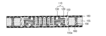
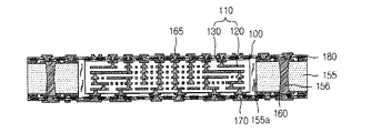
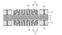
図1は、本発明の第1実施例に係るプリント回路基板を示す図である。図1を参照すると、本発明の一実施例に係るプリント回路基板は、サブ回路基板100と、コア部材155と、第1絶縁層180と、絶縁材185と、を含む。
FIG. 1 is a diagram illustrating a printed circuit board according to a first embodiment of the present invention. Referring to FIG. 1, the printed circuit board according to an embodiment of the present invention includes a
サブ回路基板100は、プリント回路基板に内蔵されるまた一つの回路基板であって、少なくとも一層の回路層と回路層の間を絶縁させる第2絶縁層とを含むことができる。サブ回路基板100は、プリント回路基板における他の領域では処理しない特定の機能を行うことができる。例えば、サブ回路基板100は、プリント回路基板に実装されるダイ(die)1と電気的に接続して電気的信号の伝逹などの機能を行うことができる。
The
ここで、ダイ1は、集積回路であって、ダイ1と接続するためには、小さな空間に非常に密集した回路が必要となる。つまり、サブ回路基板100は、微細な回路パターン120からなる高密度回路110を備えることができる。
Here, the die 1 is an integrated circuit, and in order to connect to the die 1, a very dense circuit is required in a small space. That is, the
サブ回路基板100において、高密度回路110の幅及び回路の間の間隔は、後述する低密度回路160の幅及び回路の間の間隔に比べて、狭く形成される。
In the
また、高密度回路110は、サブ回路基板100が内蔵された後に外層に形成される外層回路165よりも微細に形成することができる。例えば、高密度回路110は、半導体工程等で形成され、低密度回路160は、SAP工程(Semi−Additive Process)、M−SAP工程(Modified Semi−Additive Process)またはテンティング(tenting)工程等の基板工程により形成することができる。または、高密度回路110を、基板工程中の相対的に精密なSAP工程により形成し、低密度回路160を、相対的に、より精密でない基板工程であるM−SAP工程またはテンティング工程などにより形成することができる。
Further, the
サブ回路基板100は、コアレス(coreless)構造、すなわち、別の補強部材を中心部に有しない構造であってもよい。例えば、サブ回路基板100は、中心部に補強部材なしで微細な回路パターン120と、これを絶縁させる第2絶縁層を順に積層して形成することができる。このとき、コアレス構造のサブ回路基板100の歪み(warpage)を防止するために、サブ回路基板100に繊維補強材を備えた補強層を追加することができる。例えば、微細な回路パターン120と第2絶縁層とでビルドアップされた回路層にプリプレグ層をさらに積層してもよい。
The
サブ回路基板100は、ダイ1と直接接続されるように、一面にパッド130が形成され、パッド130とダイ1を直接結合することができる。このとき、サブ回路基板100の一面は、プリント回路基板の外層となることができる。
The
また、サブ回路基板100の一面上に付加的に外層が形成され、外層には、ダイ1と高密度回路110とを接続させる外層回路165を形成することができる。
Further, an outer layer is additionally formed on one surface of the
図1に示すように、外層回路165は、ダイ1との接続のためのパッドを含み、高密度回路110のパッド130と接続することができる。外層回路165は、微細な高密度回路110が直接ソルダリングされることで、損傷を防止することができる。
As shown in FIG. 1, the
一方、外層回路165は、高密度回路110をファンアウト(fan−out)させるファンアウト回路パターンを含むことができる。具体的に、サブ回路基板100において稠密に形成された高密度回路110は、ファンアウト回路パターンを介して低密度回路基板領域の外層に広く分散させることができる。
Meanwhile, the
ファンアウト回路パターンは、ダイ1の規格に合わせてプリント回路基板の外層に形成されたパッドを含むことができる。これにより、高密度回路110は、ダイ1の規格の影響を受けずに自由に設計できるので、高密度回路110の設計自由度を高めることができる。
The fan-out circuit pattern may include pads formed on the outer layer of the printed circuit board in accordance with the die 1 standard. As a result, the high-
サブ回路基板100は、高密度回路110に接続され、第1絶縁層180に埋め込まれる第1電子素子140を含むことができる。例えば、サブ回路基板100の外層に能動素子及び受動素子等の第1電子素子140を搭載することができる。図15に示すように、サブ回路基板100の上面にキャパシタ等の受動素子を搭載することができる。特に、ダイサイドキャパシタ(die side capacitor)等のように、従来のプリント回路基板の外層に搭載される電子素子もサブ回路基板100に搭載されることで、プリント回路基板に内蔵することができる。
The
また、サブ回路基板100は、ダイ1の機能を支援するように、マイクロ電子装置/システムのルーティング及び電力伝達機能を有する第1電子素子140を搭載することができる。
Also, the
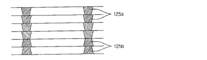
サブ回路基板100において、高密度回路110は、互いに対称に積層されたスタックビア(stack via)125a、125bを含むことができる。サブ回路基板100の歪みを低減するために、高密度回路110のビアは、中心部分を基準として両側に対称となるように積層されるビア構造を有することができる。
In the
図2は、本発明に係るプリント回路基板の高密度回路110におけるビア構造を例示する図である。
図2を参照すると、初期において幾つかの層を一方に積層し、その後、残りの層を両方に分けて連続して積層し、互いに対称なスタックビアの構造125a、125bを形成することができる。
FIG. 2 is a diagram illustrating a via structure in the high-
Referring to FIG. 2, several layers may be initially stacked on one side, and then the remaining layers may be sequentially stacked on both sides to form symmetrical stack via
コア部材155は、プリント回路基板の中心部層であり、第1絶縁層180とともにサブ回路基板100の歪み(warpage)を防止する役割を担う。このため、コア部材155は、サブ回路基板100及び第1絶縁層180よりも剛性の高い材質で形成され、コア部材155には、貫通ホールが形成されて、サブ回路基板100を内部に配置することができる。
The
例えば、コア部材155は、絶縁樹脂内にガラス繊維または炭素繊維等の補強部材が含浸された絶縁基板であってもよく、金属材質のメタルコアをコア部材155として使用できる等、その材質は様々に変更可能である。
For example, the
また、コア部材155は、貫通するビア156をさらに含むことができる。コア部材155のビア156は、コア部材155 の両側を電気的に接続させる。
The
図1を参照すると、コア部材155の上面及び下面に形成された低密度回路160は、ビア156を介して接続されることができる。
Referring to FIG. 1, the
本実施例のように、コア部材155にサブ回路基板100を内蔵する構造を有すると、サブ回路基板100が内蔵される領域においては、厚いコア構造を削除することができる。これにより、少なくともサブ回路基板100が内蔵される領域においては、コア部材155を貫通して形成されるビア156を省略することができる。コア部材155を貫通するビア156は、加工上の問題のために微細な間隔で形成することに制約がある。このため、コア部材155を貫通するビア156を省略し、サブ回路基板100のスタックビアが、コア部材155におけるビア156としての役割を担うようにすると、ビアの間のピッチを微細化することができる。また、コア構造が削除されることにより、コアの上面/下面の2層の回路層を低減することが可能となる。ビアの間隔を低減し、コアの上面/下面の回路層を低減することにより、回路ルーティング(routing)の距離を低減させ、基板全体の層数及びサイズを低減することができる。また、コア部材155のビア156と、これに接続するビアとをスタックビアで代替することにより、コア部材155のビア156と、これに接続するビアとのCTE(熱膨脹係数)差による応力発生の問題を防止することができる。
When the
第1絶縁層180は、コア部材155及びサブ回路基板100の両面に積層され、コア部材155の貫通ホールに配置されたサブ回路基板100の両面とコア部材155とを結合させることができる。
The first insulating
図1を参照すると、コア部材155がプリント回路基板の中心部層として用いられ、コア部材155の中心部分に形成された貫通ホールにサブ回路基板100を配置することができる。そして、第1絶縁層180により、コア部材155とサブ回路基板100とを結合することができる。例えば、コア部材155は、四角フレームの形状を有し、サブ回路基板100は、四角フレームの内部に配置されて内蔵される構造とすることができる。そして、両面に積層された第1絶縁層180により、コア部材155は、内蔵されたサブ回路基板100を押さえる構造を有し、サブ回路基板100の歪みを防止することができる。
Referring to FIG. 1, the
また、第1絶縁層180は、ガラス繊維(Glass cloth)等の繊維補強材を含むことができる。例えば、第1絶縁層180は、プリプレグを積層して形成することができる。ガラス繊維等の繊維補強材が含まれた第1絶縁層180は、サブ回路基板100及びコア部材155を一体にすると、サブ回路基板100の剛性をさらに補強することができる。
Further, the first insulating
絶縁材185は、貫通ホールの内壁155aとサブ回路基板100との間に充填され、サブ回路基板100の側面をコア部材155に結合することができる。
The insulating
図1を参照すると、コア部材155の貫通ホールにサブ回路基板100が配置され、貫通ホールの内壁155aとサブ回路基板100との間にはギャップが形成される。絶縁材185は、このギャップを充填するとともにコア部材155とサブ回路基板100とを結合することができる。これにより,絶縁材185は、コア部材155がサブ回路基板100の側面を押さえる構造を有することになり、サブ回路基板100の歪みを防止することができる。
Referring to FIG. 1, the
絶縁材185は、サブ回路基板100の第2絶縁層105とは異なる材質からなることができる。例えば、第1絶縁層180の絶縁物質の一部が充填されて形成されてもよい。このとき、第1絶縁層180が繊維補強材を含む場合は,絶縁材185も同じく繊維補強材を含むことができる。また、第1絶縁層180を積層する前に、貫通ホールの内壁155aとサブ回路基板100との間に、別の物質を充填して絶縁材185を形成することも可能である。
The insulating
コア部材155及び第1絶縁層180で構成された領域には、高密度回路110に比べて密度の低い低密度回路160を形成することができる。プリント回路基板において、特別な用途のために高密度回路110を必要とする部分以外の他の部分には高密度回路を構成する必要は少ない。よって、当該他の部分には、収率が高く、コストの低い低密度回路を形成することが好ましい。
A
例えば、コア部材155または第1絶縁層180のうちの少なくともいずれか1つには、内部または外部に低密度回路160を形成することができる。これにより、コア部材155、第1絶縁層180及び低密度回路160は、一体で低密度回路基板領域を形成することができ、全体的には、低密度回路基板領域が高密度回路110を備えたサブ回路基板100を内蔵する構造を有することができる。
For example, the
サブ回路基板100は、低密度回路基板領域に比べて高密度の回路層を有するため、層間隔が低密度回路基板領域における層間隔よりも狭く形成される。例えば、低密度回路基板領域のうちの1つの絶縁層に、複数層のサブ回路基板100を内蔵することができる。内蔵されたサブ回路基板100は、低密度回路基板領域の外層により覆われることができる。
Since the
また、低密度回路基板領域は、サーバ基板のフォームファクタ(form factor)に合わせて形成することが可能である。フォームファクタとは、サーバ基板等の特定の用途を有する回路基板の大きさ、構成及び物理的な配列のことをいい、ハードウェアを構成する標準となる。本発明のプリント回路基板は、低密度回路基板領域がフォームファクタに対応して形成され、サブ回路基板100は、自由に形成することができる。例えば、フォームファクタに対応する領域である低密度回路基板領域は、規格に従うレイアウトを有し、フォームファクタの以外の領域であるサブ回路基板100は、様々なサイズや形態に製作することができる。
Further, the low density circuit board region can be formed in accordance with the form factor of the server board. The form factor refers to the size, configuration, and physical arrangement of a circuit board having a specific application such as a server board, and is a standard for configuring hardware. In the printed circuit board of the present invention, the low-density circuit board region is formed corresponding to the form factor, and the
一方、低密度回路基板領域には、ダイ1サイドの部品実装空間を確保する。低密度回路基板領域には、ダイ1サイドのキャパシタ(die side capacitor)等の、サーバ基板の外層に搭載される第2電子素子190を搭載することができる。また、低密度回路基板領域には、グラウンド(GND)が形成されてもよく、グラウンドは、ビアを介してサブ回路基板100に接続することができる。
On the other hand, a component mounting space on the side of the die 1 is secured in the low density circuit board region. In the low-density circuit board region, a second
低密度回路基板領域は、低密度回路160とサブ回路基板100の高密度回路110とを接続させるビア170またはソルダーバンプをさらに含むことができる。低密度回路基板領域の低密度回路160は、サブ回路基板100側を向いたパッド及びこれに接続する回路パターンを備えることができる。図1を参照すると、ビア170を介して、低密度回路160と高密度回路110とは、上下に直接接続されることができる。これにより、信号を伝達する回路のルーティング距離が低減し、電気的信頼性を高めることができる。
The low density circuit board region may further include
図3から図14は、本発明の第1実施例に係るプリント回路基板の製造方法を示す図である。本発明の第1実施例に係るプリント回路基板の製造方法では、コア部材155を備えた低密度回路基板領域にサブ回路基板100を結合させて内蔵する方法が例示される。
3 to 14 are views showing a method of manufacturing a printed circuit board according to the first embodiment of the present invention. In the method for manufacturing a printed circuit board according to the first embodiment of the present invention, a method in which the
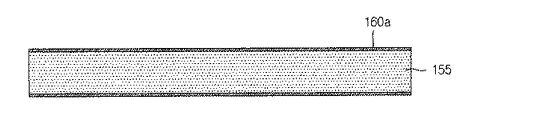
図3から図5を参照すると、金属層160aが形成されたコア部材155を準備し、コア部材155を貫通するビア156を含む低密度回路160の一部を形成することができる。このとき、サブ回路基板100が収容される部分の金属層160aを予め除去してもよい。
Referring to FIGS. 3 to 5, a
図6を参照すると、コア部材155を加工して貫通ホールCを形成することができる。
Referring to FIG. 6, the
図7を参照すると、高密度回路110が備えられたサブ回路基板100を準備し、サブ回路基板100を貫通ホールCの内部に配置することができる。サブ回路基板100を固定するために、コア部材155の一面には接着テープ155bが付着されてもよい。
Referring to FIG. 7, the
図8を参照すると、コア部材155の他面に第1絶縁層180積層し、絶縁材185を充填してサブ回路基板100を内蔵(encapsulation)することができる。第1絶縁層180の絶縁物質の一部が、貫通ホールの内壁155aとサブ回路基板100との間のギャップに充填されて絶縁材185が形成されることもできる。このとき、第1絶縁層180は、ガラス繊維等の繊維補強材を含むことができる。
Referring to FIG. 8, the first insulating
図9を参照すると、コア部材155の一面から接着テープ155bを除去し、コア部材155の一面にも第1絶縁層180を積層することができる。これにより、サブ回路基板100の両面は、第1絶縁層180によりコア部材155と強く結合され、歪みを防止することができる。
Referring to FIG. 9, the adhesive tape 155 b may be removed from one surface of the
図10及び図11を参照すると、サブ回路基板100の一面と接続する外層回路165を形成することができる。また、サブ回路基板100の他面には、ビア170及びビア170と接続する低密度回路160を形成することができる。図12を参照すると、プリント回路基板の外層にソルダーレジスト層をさらに形成することができる。
Referring to FIGS. 10 and 11, an
図13を参照すると、ソルダーレジスト層のオープニングを介してプリント回路基板の一面に露出した外層回路165にソルダーバンプを形成することができ、他面には第2電子素子190を実装することができる。
Referring to FIG. 13, solder bumps can be formed on the
図14を参照すると、プリント回路基板の一面にダイ1を実装し、ソルダーバンプにより外層回路165に接続されることができる。
Referring to FIG. 14, the die 1 can be mounted on one surface of a printed circuit board and connected to the
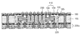
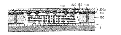
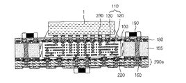
図16は、本発明の第3実施例に係るプリント回路基板を示す図である。
図16を参照すると、本発明の第3実施例に係るプリント回路基板は、サブ回路基板100の他面に積層される多層の低密度回路層200aをさらに含む構造を有する。つまり、上述した第1実施例に係るプリント回路基板を上部基板とし、多層の低密度回路層200aを下部基板として加えられた構造を有することができる。
FIG. 16 is a diagram illustrating a printed circuit board according to a third embodiment of the present invention.
Referring to FIG. 16, the printed circuit board according to the third embodiment of the present invention has a structure further including a multilayer low
多層の低密度回路層200aは、サブ回路基板100の内蔵された上部基板を支持するように接続される。多層の低密度回路層200aの回路は、ビア220を介してサブ回路基板100及び上部基板の低密度回路に接続される。多層の低密度回路層200aには、サブ回路基板100よりも厚い回路及び絶縁層が形成されるので、サブ回路基板100を内蔵する上部基板よりは高い剛性を有することができる。これにより、多層の低密度回路層200aは、サブ回路基板100及び上部基板の歪みを防止する役割を担うことができる。
The multilayer low-
図17から図25は、本発明の第3実施例に係るプリント回路基板の製造方法を示す図である。本発明の第3実施例に係るプリント回路基板の製造方法は、コア部材155と多層の低密度回路層200aとが備えられた低密度回路基板200にサブ回路基板100を結合させて内蔵する方法を例示する。
17 to 25 are views showing a method of manufacturing a printed circuit board according to the third embodiment of the present invention. A method of manufacturing a printed circuit board according to the third embodiment of the present invention is a method of incorporating a
図17及び図18を参照すると、キャリア5を準備し、キャリア5の両面に接着層6を形成することができる。図19を参照すると、キャリア5の両面に、貫通ホールC及び低密度回路160の一部が形成されたコア部材155を付着することができる。
17 and 18, the
図20を参照すると、高密度回路110が備えられたサブ回路基板100を準備し、サブ回路基板100を貫通ホールCの内部に配置することができる。このとき、本実施例におけるサブ回路基板100は、上述した第1実施例のサブ回路基板100が逆になった形態に配置される。つまり、ダイ1と接続されるサブ回路基板100の一面が、キャリア5を向くように配置される。
Referring to FIG. 20, the
図21を参照すると、コア部材155の他面に第1絶縁層180を積層し,絶縁材185を充填してサブ回路基板100を内蔵することができる。また、繊維補強材を含む第1絶縁層180をサブ回路基板100及びコア部材155に積層して、サブ回路基板100をコア部材155に、より強く結合させることができる。
Referring to FIG. 21, the first insulating
図22を参照すると、キャリア5の両面に形成された2つの上部基板のそれぞれに、多層の低密度回路層200aをさらに形成することができる。このとき、サブ回路基板100の他面には、低密度回路層200aに接続されるビア220を形成することができる。また、歪みを防止するために、多層の低密度回路層200aに繊維補強材が含まれた絶縁層を適用することができる。
Referring to FIG. 22, a multilayer low-
図23及び図24を参照すると、キャリア5を分離した後に、サブ回路基板100の一面に接続する外層回路230を形成することができる。また、プリント回路基板の外層にソルダーレジスト層をさらに形成することができる。
Referring to FIGS. 23 and 24, after separating the
図25を参照すると、ソルダーレジスト層のオープニングを介してプリント回路基板の一面に露出した外層回路にダイ1を実装することができ、他面には第2電子素子190を実装することができる。
Referring to FIG. 25, the die 1 can be mounted on the outer layer circuit exposed on one surface of the printed circuit board through the opening of the solder resist layer, and the second
以上のように、本発明の一実施例について説明したが、当該技術分野で通常の知識を有する者であれば特許請求の範囲に記載された本発明の思想から逸脱しない範囲内で、構成要素の付加、変更、削除または追加などにより本発明を多様に修正及び変更することができ、これも本発明の権利範囲内に含まれるものといえよう。 As described above, one embodiment of the present invention has been described. However, a person who has ordinary knowledge in the technical field can construct the constituent elements without departing from the spirit of the present invention described in the claims. The present invention can be variously modified and changed by adding, changing, deleting, or adding, and this is also included in the scope of the right of the present invention.
1 ダイ
5 キャリア
100 サブ回路基板
110 高密度回路
140 第1電子素子
155 コア部材
160 低密度回路
165、230 外層回路
180 第1絶縁層
185 絶縁材
190 第2電子素子
1 die 5
Claims (16)
前記貫通ホールに配置されたサブ回路基板と、
前記コア部材及び前記サブ回路基板の両面に積層された第1絶縁層と、
前記貫通ホールの内壁と前記サブ回路基板との間に充填された絶縁材と、
を含むプリント回路基板。 A core member in which a through hole is formed;
A sub circuit board disposed in the through hole;
A first insulating layer laminated on both surfaces of the core member and the sub circuit board;
An insulating material filled between the inner wall of the through hole and the sub circuit board;
Including printed circuit board.
前記コア部材及び/または前記第1絶縁層に形成され、前記高密度回路よりも密度の低い低密度回路をさらに含む請求項1から請求項8のいずれか1項に記載のプリント回路基板。 The sub-circuit board includes a high-density circuit,
9. The printed circuit board according to claim 1, further comprising a low-density circuit formed on the core member and / or the first insulating layer and having a density lower than that of the high-density circuit.
Applications Claiming Priority (4)
| Application Number | Priority Date | Filing Date | Title |
|---|---|---|---|
| KR20160002884 | 2016-01-08 | ||
| KR10-2016-0002884 | 2016-01-08 | ||
| KR1020160048927A KR20170083464A (en) | 2016-01-08 | 2016-04-21 | Printed circuit board |
| KR10-2016-0048927 | 2016-04-21 |
Publications (2)
| Publication Number | Publication Date |
|---|---|
| JP2017123459A true JP2017123459A (en) | 2017-07-13 |
| JP2017123459A5 JP2017123459A5 (en) | 2020-01-09 |
Family
ID=59276178
Family Applications (1)
| Application Number | Title | Priority Date | Filing Date |
|---|---|---|---|
| JP2016240411A Pending JP2017123459A (en) | 2016-01-08 | 2016-12-12 | Printed circuit board |
Country Status (3)
| Country | Link |
|---|---|
| US (2) | US10477683B2 (en) |
| JP (1) | JP2017123459A (en) |
| KR (1) | KR20230092854A (en) |
Cited By (5)
| Publication number | Priority date | Publication date | Assignee | Title |
|---|---|---|---|---|
| WO2020071498A1 (en) * | 2018-10-03 | 2020-04-09 | シチズン電子株式会社 | Inlay substrate and light emission device in which same is used |
| CN111883506A (en) * | 2019-05-03 | 2020-11-03 | 矽品精密工业股份有限公司 | Electronic package, bearing substrate thereof and manufacturing method |
| CN111883505A (en) * | 2019-05-03 | 2020-11-03 | 矽品精密工业股份有限公司 | Electronic package, bearing substrate thereof and manufacturing method |
| CN112216665A (en) * | 2019-07-11 | 2021-01-12 | 苏州旭创科技有限公司 | Optical module |
| CN112216672A (en) * | 2019-07-11 | 2021-01-12 | 苏州旭创科技有限公司 | Hybrid carrier plate, manufacturing method thereof, assembly and optical module |
Families Citing this family (13)
| Publication number | Priority date | Publication date | Assignee | Title |
|---|---|---|---|---|
| JP2017123459A (en) | 2016-01-08 | 2017-07-13 | サムソン エレクトロ−メカニックス カンパニーリミテッド. | Printed circuit board |
| US11394103B2 (en) * | 2017-07-18 | 2022-07-19 | Samsung Electro-Mechanics Co., Ltd. | Antenna module and manufacturing method thereof |
| WO2019026835A1 (en) * | 2017-08-04 | 2019-02-07 | 株式会社フジクラ | Method for manufacturing multilayer printed wiring board and multilayer printed wiring board |
| TWI655739B (en) * | 2018-04-19 | 2019-04-01 | 南亞電路板股份有限公司 | Package structure and forming method thereof |
| EP3644359A1 (en) * | 2018-10-23 | 2020-04-29 | AT & S Austria Technologie & Systemtechnik Aktiengesellschaft | Z-axis interconnection with protruding component |
| KR20200074693A (en) * | 2018-12-17 | 2020-06-25 | 삼성전기주식회사 | Printed circuit board |
| FR3093271B1 (en) * | 2019-02-25 | 2021-11-05 | Safran Electronics & Defense | Electronic board comprising components in cavities and shared soldering areas |
| US10978417B2 (en) * | 2019-04-29 | 2021-04-13 | Advanced Semiconductor Engineering, Inc. | Wiring structure and method for manufacturing the same |
| CN112201652A (en) * | 2019-07-07 | 2021-01-08 | 深南电路股份有限公司 | Circuit board and manufacturing method thereof |
| CN113013125A (en) * | 2019-12-20 | 2021-06-22 | 奥特斯奥地利科技与系统技术有限公司 | Component carrier with embedded insert laterally between electrically conductive structures of a stack |
| US11552015B2 (en) * | 2020-06-12 | 2023-01-10 | Qualcomm Incorporated | Substrate comprising a high-density interconnect portion embedded in a core layer |
| US11948918B2 (en) * | 2020-06-15 | 2024-04-02 | Taiwan Semiconductor Manufacturing Co., Ltd. | Redistribution structure for semiconductor device and method of forming same |
| TWI778816B (en) | 2021-09-28 | 2022-09-21 | 欣興電子股份有限公司 | Package structure with interconnection between chips and package method thereof |
Citations (5)
| Publication number | Priority date | Publication date | Assignee | Title |
|---|---|---|---|---|
| WO2009141928A1 (en) * | 2008-05-19 | 2009-11-26 | イビデン株式会社 | Printed wiring board and method for manufacturing the same |
| WO2011102561A1 (en) * | 2010-02-22 | 2011-08-25 | 三洋電機株式会社 | Multilayer printed circuit board and manufacturing method therefor |
| JP2012099610A (en) * | 2010-11-01 | 2012-05-24 | Shinko Electric Ind Co Ltd | Wiring board and method of manufacturing the same, and method of manufacturing semiconductor package |
| JP2013140963A (en) * | 2011-12-29 | 2013-07-18 | Troisd Plus | Method for collective fabrication of 3d electronic module including only validated printed circuit board |
| JP2014207308A (en) * | 2013-04-12 | 2014-10-30 | 日本電気株式会社 | Multilayer wiring board and method of manufacturing the same |
Family Cites Families (63)
| Publication number | Priority date | Publication date | Assignee | Title |
|---|---|---|---|---|
| US5081563A (en) * | 1990-04-27 | 1992-01-14 | International Business Machines Corporation | Multi-layer package incorporating a recessed cavity for a semiconductor chip |
| US5310965A (en) * | 1991-08-28 | 1994-05-10 | Nec Corporation | Multi-level wiring structure having an organic interlayer insulating film |
| JPH11317582A (en) | 1998-02-16 | 1999-11-16 | Matsushita Electric Ind Co Ltd | Multilayer wiring board and manufacture thereof |
| US6281446B1 (en) * | 1998-02-16 | 2001-08-28 | Matsushita Electric Industrial Co., Ltd. | Multi-layered circuit board and method of manufacturing the same |
| JP3807312B2 (en) * | 2002-01-18 | 2006-08-09 | 富士通株式会社 | Printed circuit board and manufacturing method thereof |
| US8076782B2 (en) * | 2002-04-01 | 2011-12-13 | Ibiden Co., Ltd. | Substrate for mounting IC chip |
| US7834273B2 (en) * | 2005-07-07 | 2010-11-16 | Ibiden Co., Ltd. | Multilayer printed wiring board |
| US7932471B2 (en) * | 2005-08-05 | 2011-04-26 | Ngk Spark Plug Co., Ltd. | Capacitor for incorporation in wiring board, wiring board, method of manufacturing wiring board, and ceramic chip for embedment |
| JP4546415B2 (en) * | 2005-09-01 | 2010-09-15 | 日本特殊陶業株式会社 | Wiring board, ceramic capacitor |
| JP4509972B2 (en) * | 2005-09-01 | 2010-07-21 | 日本特殊陶業株式会社 | Wiring board, embedded ceramic chip |
| US7742314B2 (en) * | 2005-09-01 | 2010-06-22 | Ngk Spark Plug Co., Ltd. | Wiring board and capacitor |
| EP1806323A1 (en) * | 2006-01-05 | 2007-07-11 | Biothane Systems International B.V. | Process and reactor for anaerobic waste water purification |
| US7808799B2 (en) * | 2006-04-25 | 2010-10-05 | Ngk Spark Plug Co., Ltd. | Wiring board |
| TWI407870B (en) * | 2006-04-25 | 2013-09-01 | Ngk Spark Plug Co | Method for manufacturing wiring board |
| JPWO2008053833A1 (en) * | 2006-11-03 | 2010-02-25 | イビデン株式会社 | Multilayer printed wiring board |
| US20080239685A1 (en) * | 2007-03-27 | 2008-10-02 | Tadahiko Kawabe | Capacitor built-in wiring board |
| US7919849B2 (en) * | 2007-04-04 | 2011-04-05 | Ibiden Co., Ltd. | Package substrate and device for optical communication |
| US8072732B2 (en) * | 2007-04-10 | 2011-12-06 | Ngk Spark Plug Co., Ltd. | Capacitor and wiring board including the capacitor |
| EP2141972B1 (en) * | 2007-05-02 | 2014-04-02 | Murata Manufacturing Co. Ltd. | Component-incorporating module and its manufacturing method |
| US7936567B2 (en) * | 2007-05-07 | 2011-05-03 | Ngk Spark Plug Co., Ltd. | Wiring board with built-in component and method for manufacturing the same |
| US8314343B2 (en) * | 2007-09-05 | 2012-11-20 | Taiyo Yuden Co., Ltd. | Multi-layer board incorporating electronic component and method for producing the same |
| US7829794B2 (en) * | 2007-09-13 | 2010-11-09 | 3M Innovative Properties Company | Partially rigid flexible circuits and method of making same |
| US8159832B2 (en) * | 2007-09-21 | 2012-04-17 | Nokia Corporation | Electromagnetic band gap structures and method for making same |
| US7935893B2 (en) * | 2008-02-14 | 2011-05-03 | Ibiden Co., Ltd. | Method of manufacturing printed wiring board with built-in electronic component |
| EP2259669A4 (en) * | 2008-03-24 | 2011-12-28 | Ngk Spark Plug Co | Component-incorporating wiring board |
| WO2009141927A1 (en) * | 2008-05-23 | 2009-11-26 | イビデン株式会社 | Printed wiring board and method for manufacturing the same |
| TWI443789B (en) * | 2008-07-04 | 2014-07-01 | Unimicron Technology Corp | Substrate having semiconductor chip embedded therein and fabrication method thereof |
| JP2010034199A (en) * | 2008-07-28 | 2010-02-12 | Fujitsu Ltd | Printed wiring board |
| JP2010114434A (en) * | 2008-10-08 | 2010-05-20 | Ngk Spark Plug Co Ltd | Component built-in wiring board and method of manufacturing the same |
| KR101638957B1 (en) * | 2009-01-13 | 2016-07-14 | 삼성전자주식회사 | Display device and method for program reservating |
| US8654539B2 (en) * | 2009-12-15 | 2014-02-18 | Ngk Spark Plug Co., Ltd. | Capacitor-incorporated substrate and component-incorporated wiring substrate |
| US8493747B2 (en) * | 2010-02-05 | 2013-07-23 | Ibiden Co., Ltd. | Flex-rigid wiring board and method for manufacturing the same |
| US8541693B2 (en) * | 2010-03-31 | 2013-09-24 | Ibiden Co., Ltd. | Wiring board and method for manufacturing the same |
| US8530755B2 (en) * | 2010-03-31 | 2013-09-10 | Ibiden Co., Ltd. | Wiring board and method for manufacturing the same |
| US8519270B2 (en) * | 2010-05-19 | 2013-08-27 | Unimicron Technology Corp. | Circuit board and manufacturing method thereof |
| JP5273320B2 (en) * | 2010-11-29 | 2013-08-28 | 株式会社村田製作所 | Multilayer flexible board |
| JP2012151372A (en) * | 2011-01-20 | 2012-08-09 | Ibiden Co Ltd | Wiring board and manufacturing method of the same |
| US8754514B2 (en) | 2011-08-10 | 2014-06-17 | Taiwan Semiconductor Manufacturing Company, Ltd. | Multi-chip wafer level package |
| US20130048355A1 (en) * | 2011-08-30 | 2013-02-28 | Ibiden Co., Ltd. | Printed wiring board |
| US9040837B2 (en) * | 2011-12-14 | 2015-05-26 | Ibiden Co., Ltd. | Wiring board and method for manufacturing the same |
| KR20130089475A (en) * | 2012-02-02 | 2013-08-12 | 삼성전자주식회사 | Circuit board, method for fabricating the same and semiconductor package using the same |
| US9287034B2 (en) * | 2012-02-27 | 2016-03-15 | Ibiden Co., Ltd. | Printed wiring board, inductor component, and method for manufacturing inductor component |
| JP2013229526A (en) * | 2012-04-26 | 2013-11-07 | Ngk Spark Plug Co Ltd | Multilayer wiring board and method of manufacturing the same |
| JP6133549B2 (en) * | 2012-04-26 | 2017-05-24 | 新光電気工業株式会社 | Wiring board and method of manufacturing wiring board |
| CN204231766U (en) * | 2012-06-14 | 2015-03-25 | 株式会社村田制作所 | High-frequency model |
| KR101926072B1 (en) * | 2012-08-21 | 2018-12-07 | 삼성디스플레이 주식회사 | Flexible display device |
| JP2014090080A (en) * | 2012-10-30 | 2014-05-15 | Ibiden Co Ltd | Printed wiring board, printed wiring board manufacturing method ane electronic component |
| JP6057681B2 (en) * | 2012-11-21 | 2017-01-11 | 新光電気工業株式会社 | Wiring board and manufacturing method thereof |
| KR20140081193A (en) | 2012-12-21 | 2014-07-01 | 삼성전기주식회사 | Hybrid substrate with high density and low density substrate area and manufacturing method thereof |
| JP2015018979A (en) * | 2013-07-12 | 2015-01-29 | イビデン株式会社 | Printed wiring board |
| JP2015028986A (en) * | 2013-07-30 | 2015-02-12 | イビデン株式会社 | Printed wiring board and printed wiring board manufacturing method |
| JP5583828B1 (en) * | 2013-08-05 | 2014-09-03 | 株式会社フジクラ | Electronic component built-in multilayer wiring board and method for manufacturing the same |
| KR102093156B1 (en) * | 2013-09-02 | 2020-03-25 | 삼성전기주식회사 | Rigid Flexible PCB and manufacture Method of It |
| US9443764B2 (en) * | 2013-10-11 | 2016-09-13 | GlobalFoundries, Inc. | Method of eliminating poor reveal of through silicon vias |
| JP6287149B2 (en) * | 2013-12-10 | 2018-03-07 | イビデン株式会社 | Electronic component built-in substrate and manufacturing method of electronic component built-in substrate |
| JP2015185564A (en) * | 2014-03-20 | 2015-10-22 | イビデン株式会社 | Printed wiring board and method for manufacturing printed wiring board |
| JP2015220281A (en) * | 2014-05-15 | 2015-12-07 | イビデン株式会社 | Printed wiring board |
| JP2016051847A (en) * | 2014-09-01 | 2016-04-11 | イビデン株式会社 | Printed wiring board, manufacturing method of the same and semiconductor device |
| US9736939B2 (en) * | 2014-09-19 | 2017-08-15 | Samsung Electro-Mechanics Co., Ltd. | Printed circuit board and method of manufacturing printed circuit board |
| JP2016082163A (en) * | 2014-10-21 | 2016-05-16 | イビデン株式会社 | Printed wiring board |
| JP6503687B2 (en) * | 2014-10-23 | 2019-04-24 | イビデン株式会社 | Printed wiring board |
| KR20170062123A (en) * | 2015-11-27 | 2017-06-07 | 삼성전기주식회사 | Fingerprint sensing device |
| JP2017123459A (en) * | 2016-01-08 | 2017-07-13 | サムソン エレクトロ−メカニックス カンパニーリミテッド. | Printed circuit board |
-
2016
- 2016-12-12 JP JP2016240411A patent/JP2017123459A/en active Pending
-
2017
- 2017-01-06 US US15/400,606 patent/US10477683B2/en active Active
-
2019
- 2019-09-30 US US16/587,169 patent/US10701806B2/en active Active
-
2023
- 2023-06-15 KR KR1020230076819A patent/KR20230092854A/en not_active Application Discontinuation
Patent Citations (5)
| Publication number | Priority date | Publication date | Assignee | Title |
|---|---|---|---|---|
| WO2009141928A1 (en) * | 2008-05-19 | 2009-11-26 | イビデン株式会社 | Printed wiring board and method for manufacturing the same |
| WO2011102561A1 (en) * | 2010-02-22 | 2011-08-25 | 三洋電機株式会社 | Multilayer printed circuit board and manufacturing method therefor |
| JP2012099610A (en) * | 2010-11-01 | 2012-05-24 | Shinko Electric Ind Co Ltd | Wiring board and method of manufacturing the same, and method of manufacturing semiconductor package |
| JP2013140963A (en) * | 2011-12-29 | 2013-07-18 | Troisd Plus | Method for collective fabrication of 3d electronic module including only validated printed circuit board |
| JP2014207308A (en) * | 2013-04-12 | 2014-10-30 | 日本電気株式会社 | Multilayer wiring board and method of manufacturing the same |
Cited By (8)
| Publication number | Priority date | Publication date | Assignee | Title |
|---|---|---|---|---|
| WO2020071498A1 (en) * | 2018-10-03 | 2020-04-09 | シチズン電子株式会社 | Inlay substrate and light emission device in which same is used |
| JPWO2020071498A1 (en) * | 2018-10-03 | 2021-09-02 | シチズン電子株式会社 | Inlay board and light emitting device using it |
| JP7074872B2 (en) | 2018-10-03 | 2022-05-24 | シチズン電子株式会社 | Inlay board and light emitting device using it |
| CN111883506A (en) * | 2019-05-03 | 2020-11-03 | 矽品精密工业股份有限公司 | Electronic package, bearing substrate thereof and manufacturing method |
| CN111883505A (en) * | 2019-05-03 | 2020-11-03 | 矽品精密工业股份有限公司 | Electronic package, bearing substrate thereof and manufacturing method |
| CN111883506B (en) * | 2019-05-03 | 2022-09-06 | 矽品精密工业股份有限公司 | Electronic package, bearing substrate thereof and manufacturing method |
| CN112216665A (en) * | 2019-07-11 | 2021-01-12 | 苏州旭创科技有限公司 | Optical module |
| CN112216672A (en) * | 2019-07-11 | 2021-01-12 | 苏州旭创科技有限公司 | Hybrid carrier plate, manufacturing method thereof, assembly and optical module |
Also Published As
| Publication number | Publication date |
|---|---|
| US20200029435A1 (en) | 2020-01-23 |
| US10701806B2 (en) | 2020-06-30 |
| US20170202083A1 (en) | 2017-07-13 |
| KR20230092854A (en) | 2023-06-26 |
| US10477683B2 (en) | 2019-11-12 |
Similar Documents
| Publication | Publication Date | Title |
|---|---|---|
| JP2017123459A (en) | Printed circuit board | |
| JP5389770B2 (en) | Printed circuit board with built-in electronic element and manufacturing method thereof | |
| JP6504665B2 (en) | Printed circuit board, method of manufacturing the same, and electronic component module | |
| KR20080076241A (en) | Printed circuit board having electronic component and method for manufacturing thereof | |
| KR101155624B1 (en) | Embedded pcb and manufacturing method for the same | |
| JP2008166327A (en) | Wiring board and its manufacturing method, and semiconductor device | |
| JP2015005612A (en) | Package substrate, and manufacturing method therefor | |
| JP2009277916A (en) | Wiring board, manufacturing method thereof, and semiconductor package | |
| JP2015149477A (en) | Embedded board, printed circuit board and method of manufacturing the same | |
| KR102134933B1 (en) | Wiring substrate and wiring substrate fabrication method | |
| JP2016054222A (en) | Multilayer wiring board | |
| US10219374B2 (en) | Printed wiring board | |
| KR100972431B1 (en) | Embedded printed circuit board and manufacturing method thereof | |
| JP2009044124A (en) | Multi-layer printed circuit board and method for manufacturing the same | |
| JP7002321B2 (en) | Wiring board | |
| JP7272527B2 (en) | printed circuit board | |
| KR20170083464A (en) | Printed circuit board | |
| JP2006049762A (en) | Part built-in substrate and manufacturing method thereof | |
| US20230137841A1 (en) | Circuit carrier and manufacturing method thereof and package structure | |
| JP7128098B2 (en) | wiring board | |
| WO2021044675A1 (en) | Substrate, method for manufacturing substrate, and electronic device | |
| KR102023729B1 (en) | printed circuit board and method of manufacturing the same | |
| JP2020053562A (en) | Printed wiring board and manufacturing method thereof | |
| JP2020053560A (en) | Manufacturing method of printed wiring board | |
| KR101077358B1 (en) | A carrier member for manufacturing a substrate and a method of manufacturing a substrate using the same |
Legal Events
| Date | Code | Title | Description |
|---|---|---|---|
| A521 | Request for written amendment filed |
Free format text: JAPANESE INTERMEDIATE CODE: A523 Effective date: 20191118 |
|
| A621 | Written request for application examination |
Free format text: JAPANESE INTERMEDIATE CODE: A621 Effective date: 20191118 |
|
| A977 | Report on retrieval |
Free format text: JAPANESE INTERMEDIATE CODE: A971007 Effective date: 20200910 |
|
| A131 | Notification of reasons for refusal |
Free format text: JAPANESE INTERMEDIATE CODE: A131 Effective date: 20200929 |
|
| A521 | Request for written amendment filed |
Free format text: JAPANESE INTERMEDIATE CODE: A523 Effective date: 20201228 |
|
| A131 | Notification of reasons for refusal |
Free format text: JAPANESE INTERMEDIATE CODE: A131 Effective date: 20210330 |
|
| A521 | Request for written amendment filed |
Free format text: JAPANESE INTERMEDIATE CODE: A523 Effective date: 20210628 |
|
| A02 | Decision of refusal |
Free format text: JAPANESE INTERMEDIATE CODE: A02 Effective date: 20211130 |
|
| A521 | Request for written amendment filed |
Free format text: JAPANESE INTERMEDIATE CODE: A523 Effective date: 20220323 |
|
| C60 | Trial request (containing other claim documents, opposition documents) |
Free format text: JAPANESE INTERMEDIATE CODE: C60 Effective date: 20220323 |
|
| A911 | Transfer to examiner for re-examination before appeal (zenchi) |
Free format text: JAPANESE INTERMEDIATE CODE: A911 Effective date: 20220401 |
|
| C21 | Notice of transfer of a case for reconsideration by examiners before appeal proceedings |
Free format text: JAPANESE INTERMEDIATE CODE: C21 Effective date: 20220405 |
|
| A912 | Re-examination (zenchi) completed and case transferred to appeal board |
Free format text: JAPANESE INTERMEDIATE CODE: A912 Effective date: 20220610 |
|
| C211 | Notice of termination of reconsideration by examiners before appeal proceedings |
Free format text: JAPANESE INTERMEDIATE CODE: C211 Effective date: 20220614 |
|
| C22 | Notice of designation (change) of administrative judge |
Free format text: JAPANESE INTERMEDIATE CODE: C22 Effective date: 20221206 |
|
| C23 | Notice of termination of proceedings |
Free format text: JAPANESE INTERMEDIATE CODE: C23 Effective date: 20230207 |
|
| C03 | Trial/appeal decision taken |
Free format text: JAPANESE INTERMEDIATE CODE: C03 Effective date: 20230307 |
|
| C30A | Notification sent |
Free format text: JAPANESE INTERMEDIATE CODE: C3012 Effective date: 20230307 |