JP2008166327A - WIRING BOARD, MANUFACTURING METHOD THEREOF, AND SEMICONDUCTOR DEVICE - Google Patents
WIRING BOARD, MANUFACTURING METHOD THEREOF, AND SEMICONDUCTOR DEVICE Download PDFInfo
- Publication number
- JP2008166327A JP2008166327A JP2006351000A JP2006351000A JP2008166327A JP 2008166327 A JP2008166327 A JP 2008166327A JP 2006351000 A JP2006351000 A JP 2006351000A JP 2006351000 A JP2006351000 A JP 2006351000A JP 2008166327 A JP2008166327 A JP 2008166327A
- Authority
- JP
- Japan
- Prior art keywords
- wiring board
- wiring
- silicon interposer
- interposer
- base
- Prior art date
- Legal status (The legal status is an assumption and is not a legal conclusion. Google has not performed a legal analysis and makes no representation as to the accuracy of the status listed.)
- Granted
Links
Images

Classifications
-
- H—ELECTRICITY
- H10—SEMICONDUCTOR DEVICES; ELECTRIC SOLID-STATE DEVICES NOT OTHERWISE PROVIDED FOR
- H10W—GENERIC PACKAGES, INTERCONNECTIONS, CONNECTORS OR OTHER CONSTRUCTIONAL DETAILS OF DEVICES COVERED BY CLASS H10
- H10W74/00—Encapsulations, e.g. protective coatings
- H10W74/10—Encapsulations, e.g. protective coatings characterised by their shape or disposition
- H10W74/111—Encapsulations, e.g. protective coatings characterised by their shape or disposition the semiconductor body being completely enclosed
- H10W74/114—Encapsulations, e.g. protective coatings characterised by their shape or disposition the semiconductor body being completely enclosed by a substrate and the encapsulations
- H10W74/117—Encapsulations, e.g. protective coatings characterised by their shape or disposition the semiconductor body being completely enclosed by a substrate and the encapsulations the substrate having spherical bumps for external connection
-
- H—ELECTRICITY
- H10—SEMICONDUCTOR DEVICES; ELECTRIC SOLID-STATE DEVICES NOT OTHERWISE PROVIDED FOR
- H10W—GENERIC PACKAGES, INTERCONNECTIONS, CONNECTORS OR OTHER CONSTRUCTIONAL DETAILS OF DEVICES COVERED BY CLASS H10
- H10W74/00—Encapsulations, e.g. protective coatings
- H10W74/01—Manufacture or treatment
- H10W74/016—Manufacture or treatment using moulds
-
- H—ELECTRICITY
- H10—SEMICONDUCTOR DEVICES; ELECTRIC SOLID-STATE DEVICES NOT OTHERWISE PROVIDED FOR
- H10W—GENERIC PACKAGES, INTERCONNECTIONS, CONNECTORS OR OTHER CONSTRUCTIONAL DETAILS OF DEVICES COVERED BY CLASS H10
- H10W90/00—Package configurations
- H10W90/401—Package configurations characterised by multiple insulating or insulated package substrates, interposers or RDLs
-
- H—ELECTRICITY
- H10—SEMICONDUCTOR DEVICES; ELECTRIC SOLID-STATE DEVICES NOT OTHERWISE PROVIDED FOR
- H10W—GENERIC PACKAGES, INTERCONNECTIONS, CONNECTORS OR OTHER CONSTRUCTIONAL DETAILS OF DEVICES COVERED BY CLASS H10
- H10W70/00—Package substrates; Interposers; Redistribution layers [RDL]
- H10W70/60—Insulating or insulated package substrates; Interposers; Redistribution layers
- H10W70/62—Insulating or insulated package substrates; Interposers; Redistribution layers characterised by their interconnections
- H10W70/63—Vias, e.g. via plugs
- H10W70/635—Through-vias
-
- H—ELECTRICITY
- H10—SEMICONDUCTOR DEVICES; ELECTRIC SOLID-STATE DEVICES NOT OTHERWISE PROVIDED FOR
- H10W—GENERIC PACKAGES, INTERCONNECTIONS, CONNECTORS OR OTHER CONSTRUCTIONAL DETAILS OF DEVICES COVERED BY CLASS H10
- H10W70/00—Package substrates; Interposers; Redistribution layers [RDL]
- H10W70/60—Insulating or insulated package substrates; Interposers; Redistribution layers
- H10W70/67—Insulating or insulated package substrates; Interposers; Redistribution layers characterised by their insulating layers or insulating parts
- H10W70/69—Insulating materials thereof
- H10W70/698—Semiconductor materials that are electrically insulating, e.g. undoped silicon
-
- H—ELECTRICITY
- H10—SEMICONDUCTOR DEVICES; ELECTRIC SOLID-STATE DEVICES NOT OTHERWISE PROVIDED FOR
- H10W—GENERIC PACKAGES, INTERCONNECTIONS, CONNECTORS OR OTHER CONSTRUCTIONAL DETAILS OF DEVICES COVERED BY CLASS H10
- H10W72/00—Interconnections or connectors in packages
-
- H—ELECTRICITY
- H10—SEMICONDUCTOR DEVICES; ELECTRIC SOLID-STATE DEVICES NOT OTHERWISE PROVIDED FOR
- H10W—GENERIC PACKAGES, INTERCONNECTIONS, CONNECTORS OR OTHER CONSTRUCTIONAL DETAILS OF DEVICES COVERED BY CLASS H10
- H10W72/00—Interconnections or connectors in packages
- H10W72/90—Bond pads, in general
- H10W72/921—Structures or relative sizes of bond pads
- H10W72/923—Bond pads having multiple stacked layers
-
- H—ELECTRICITY
- H10—SEMICONDUCTOR DEVICES; ELECTRIC SOLID-STATE DEVICES NOT OTHERWISE PROVIDED FOR
- H10W—GENERIC PACKAGES, INTERCONNECTIONS, CONNECTORS OR OTHER CONSTRUCTIONAL DETAILS OF DEVICES COVERED BY CLASS H10
- H10W72/00—Interconnections or connectors in packages
- H10W72/90—Bond pads, in general
- H10W72/941—Dispositions of bond pads
- H10W72/9415—Dispositions of bond pads relative to the surface, e.g. recessed, protruding
-
- H—ELECTRICITY
- H10—SEMICONDUCTOR DEVICES; ELECTRIC SOLID-STATE DEVICES NOT OTHERWISE PROVIDED FOR
- H10W—GENERIC PACKAGES, INTERCONNECTIONS, CONNECTORS OR OTHER CONSTRUCTIONAL DETAILS OF DEVICES COVERED BY CLASS H10
- H10W90/00—Package configurations
- H10W90/701—Package configurations characterised by the relative positions of pads or connectors relative to package parts
- H10W90/721—Package configurations characterised by the relative positions of pads or connectors relative to package parts of bump connectors
- H10W90/724—Package configurations characterised by the relative positions of pads or connectors relative to package parts of bump connectors between a chip and a stacked insulating package substrate, interposer or RDL
-
- Y—GENERAL TAGGING OF NEW TECHNOLOGICAL DEVELOPMENTS; GENERAL TAGGING OF CROSS-SECTIONAL TECHNOLOGIES SPANNING OVER SEVERAL SECTIONS OF THE IPC; TECHNICAL SUBJECTS COVERED BY FORMER USPC CROSS-REFERENCE ART COLLECTIONS [XRACs] AND DIGESTS
- Y10—TECHNICAL SUBJECTS COVERED BY FORMER USPC
- Y10T—TECHNICAL SUBJECTS COVERED BY FORMER US CLASSIFICATION
- Y10T29/00—Metal working
- Y10T29/49—Method of mechanical manufacture
- Y10T29/49002—Electrical device making
- Y10T29/49117—Conductor or circuit manufacturing
- Y10T29/49124—On flat or curved insulated base, e.g., printed circuit, etc.
- Y10T29/49126—Assembling bases
Landscapes
- Production Of Multi-Layered Print Wiring Board (AREA)
- Non-Metallic Protective Coatings For Printed Circuits (AREA)
- Structures For Mounting Electric Components On Printed Circuit Boards (AREA)
Abstract
【課題】シリコンインターポーザの仕様に対応させて配線パターンの層数を必要最小限に設定できると共に、製造工程が簡略化されて低コスト・高歩留りで製造される、シリコンインターポーザ内蔵配線基板を提供する。
【解決手段】上下側を導通可能にする配線パターン16を備えた複数のユニット配線板10,20が、接続端子20aを介して接続されて積層されてベース配線板5が構成され、ベース配線板5の上にシリコンインターポーザ30が接続端子30aを介して接続されて積層されている。複数のユニット配線板10、20の間の隙間、及びベース配線板5とシリコンインターポーザ30との隙間に真空トランスファモールド法によって樹脂部50が充填されており、樹脂部50はベース配線板5及びシリコンインターポーザ30を一体化する基板として機能する。
【選択図】図8Provided is a wiring substrate with a built-in silicon interposer that can be set to the minimum necessary number of wiring pattern layers corresponding to the specifications of a silicon interposer and that is manufactured at a low cost and with a high yield by simplifying the manufacturing process. .
A plurality of unit wiring boards (10, 20) having wiring patterns (16) that allow conduction on the upper and lower sides are connected and stacked via connection terminals (20a) to form a base wiring board (5). A silicon interposer 30 is stacked on the substrate 5 via a connection terminal 30a. The gap between the plurality of unit wiring boards 10 and 20 and the gap between the base wiring board 5 and the silicon interposer 30 are filled with the resin part 50 by a vacuum transfer molding method. It functions as a substrate on which the interposer 30 is integrated.
[Selection] Figure 8
Description
本発明は配線基板及びその製造方法と半導体装置に係り、さらに詳しくは、高性能な半導体チップの実装に対応できるシリコンインターポーザが内蔵された配線基板及びその製造方法と半導体装置に関する。 The present invention relates to a wiring board, a manufacturing method thereof, and a semiconductor device, and more particularly to a wiring board with a built-in silicon interposer that can be used for mounting a high-performance semiconductor chip, a manufacturing method thereof, and a semiconductor device.
従来、CPUなどの半導体チップが配線基板の上に実装されて構成される半導体装置がある。半導体チップを実装するための配線基板としては、ファインピッチの配線が多層化されて形成されたビルドアップ配線板が一般的に使用されている。 Conventionally, there is a semiconductor device configured by mounting a semiconductor chip such as a CPU on a wiring board. As a wiring board for mounting a semiconductor chip, a build-up wiring board formed by multilayering fine pitch wiring is generally used.
近年では、半導体チップのさらなる高性能化に伴ってその接続電極のピッチが狭小化されてきている。ビルドアップ配線板の配線のファインピッチ化には限界があるので、そのような半導体チップをビルドアップ配線板に直接実装することが困難になりつつある。その対策として、上下側を導通可能にする微細配線を備えたシリコンインターポーザを介して半導体チップをビルドアップ配線板に接続する方法が提案されている。 In recent years, the pitch of the connection electrodes has been narrowed as the performance of semiconductor chips is further improved. Since there is a limit to the fine pitch of the wiring of the build-up wiring board, it is becoming difficult to directly mount such a semiconductor chip on the build-up wiring board. As a countermeasure, there has been proposed a method of connecting a semiconductor chip to a build-up wiring board via a silicon interposer provided with fine wiring that allows conduction on the upper and lower sides.
特許文献1には、半導体チップ内の配線層数を減らすために半導体チップ内の配線の機能をインターポーザに移し、配線基板の上にインターポーザを介して半導体チップを実装することが記載されている。 Patent Document 1 describes that in order to reduce the number of wiring layers in a semiconductor chip, the function of wiring in the semiconductor chip is transferred to an interposer, and the semiconductor chip is mounted on the wiring board via the interposer.
特許文献2には、外部接続端子を備えた第1の配線基板に半導体素子が実装された上部装置部と、接続用電極を備えた第2の配線基板に半導体素子が実装された下部装置部との間に、インターポーザ基板を配設することが記載されている。
前述したように、半導体チップの高性能化に伴ってビルドアップ配線板の配線のさらなるファインピッチ化や多層化、さらにはシリコンインターポーザの導入が必要となり、これによって半導体装置のコスト上昇や歩留り低下を招きやすい。 As described above, with higher performance of semiconductor chips, it is necessary to further increase the pitch and multilayer of the wiring of the build-up wiring board, and to introduce a silicon interposer, which increases the cost and yield of semiconductor devices. Easy to invite.
例えば、ビルドアップ配線板のスルーホールランドから配線を引き回してシリコンインターポーザが接続されるインターポーザ用パッドを配置する際に、配線の引き回しの途中でスルーホールランドが邪魔になって配線を引き回せない場合は、ビルドアップ配線板の配線の層数を増やして対応する必要がある。 For example, when placing an interposer pad to which a silicon interposer is connected by routing the wiring from the through-hole land of the build-up wiring board, the wiring cannot be routed due to the through-hole land in the middle of the wiring Needs to be handled by increasing the number of wiring layers of the build-up wiring board.
このとき、従来技術のビルドアップ配線板では、片面側の配線の追加のみで対応できる場合であっても、反りの発生を防止するためにコア基板の両面側に配線を対称に形成する必要があり、無駄なコストがかかる問題がある。 At this time, in the build-up wiring board of the prior art, it is necessary to form the wiring symmetrically on both sides of the core substrate in order to prevent the occurrence of warping even when only the addition of the wiring on one side is possible. There is a problem of costly use.
このように、従来技術のビルドアップ配線板では、半導体チップの高性能化に対応させる際に、不必要な配線を形成する必要があることから配線の層数が膨大になるケースが想定され、コスト上昇や歩留りの低下が懸念される。さらには、ビルドアップ配線板の上にシリコンインターポーザを接続してインターポーザ内蔵配線基板を構成する際に、高い信頼性が得られる構造が要求される。 In this way, in the build-up wiring board of the prior art, it is assumed that the number of wiring layers becomes enormous because it is necessary to form unnecessary wiring when dealing with high performance of the semiconductor chip, There are concerns about cost increase and yield decrease. Furthermore, when a silicon interposer is connected on the build-up wiring board to form a wiring board with a built-in interposer, a structure capable of obtaining high reliability is required.
本発明は以上の課題を鑑みて創作されたものであり、シリコンインターポーザを内蔵する配線基板において、シリコンインターポーザの仕様に対応させて配線パターンの層数を必要最小限に設定できると共に、製造工程が簡略化されて低コスト・高歩留りで製造される信頼性の高い配線基板及びその製造方法と半導体装置を提供することを目的とする。 The present invention was created in view of the above problems, and in a wiring board incorporating a silicon interposer, the number of wiring pattern layers can be set to the minimum necessary in accordance with the specifications of the silicon interposer, and the manufacturing process It is an object of the present invention to provide a highly reliable wiring board that is simplified and manufactured at a low cost and a high yield, a manufacturing method thereof, and a semiconductor device.
上記課題を解決するため、本発明は配線基板に係り、上下側を導通可能にする配線パターンを備えた複数のユニット配線板が、接続端子を介して相互接続されて積層されて構成されるベース配線板と、前記ベース配線板の上に積層され、上下側を導通可能にする配線パターンを備えて、前記ベース配線板の前記配線パターンに接続端子を介して接続されたシリコンインターポーザと、前記複数のユニット配線板の間の隙間、及び前記ベース配線板と前記シリコンインターポーザとの隙間に充填され、前記ベース配線板及び前記シリコンインターポーザを一体化する樹脂部とを有することを特徴とする。 In order to solve the above-described problems, the present invention relates to a wiring board, and a base comprising a plurality of unit wiring boards each having a wiring pattern that allows conduction on the upper and lower sides, which are interconnected and stacked via connection terminals. A wiring board; a silicon interposer that is stacked on the base wiring board and includes a wiring pattern that allows conduction between the upper and lower sides; and is connected to the wiring pattern of the base wiring board via a connection terminal; A gap between the unit wiring boards and a gap between the base wiring board and the silicon interposer, and a resin portion for integrating the base wiring board and the silicon interposer.
本発明の配線基板を構成するベース配線板は、上下側を導通可能にする配線パターンを備えた複数のユニット配線板が厚さ方向に積層されて接続端子を介して相互接続されて構成される。ベース配線板の上には高性能な半導体チップが実装される微細配線を備えたシリコンインターポーザが接続端子を介して接続されている。 The base wiring board constituting the wiring board of the present invention is configured by laminating a plurality of unit wiring boards having wiring patterns that enable conduction on the upper and lower sides and interconnecting them through connection terminals. . On the base wiring board, a silicon interposer having fine wiring on which a high-performance semiconductor chip is mounted is connected via a connection terminal.
さらに、複数のユニット配線板の隙間及びベース配線板とシリコンインターポーザとの隙間に樹脂部が充填されており、樹脂部がベース配線板及びシリコンインターポーザを一体化する基板として機能する。シリコンインターポーザはその上面の半導体チップ搭載面が露出した状態で樹脂部に埋設されている。 Further, a resin portion is filled in a gap between the plurality of unit wiring boards and a gap between the base wiring board and the silicon interposer, and the resin part functions as a substrate for integrating the base wiring board and the silicon interposer. The silicon interposer is embedded in the resin part with the semiconductor chip mounting surface on the upper surface exposed.
本発明の配線基板では、高性能な半導体チップの狭小ピッチの接続電極が微細配線を備えたシリコンインターポーザに接続され、シリコンインターポーザからベース配線板にピッチ変換される。 In the wiring board of the present invention, the narrow pitch connection electrodes of the high performance semiconductor chip are connected to the silicon interposer provided with the fine wiring, and the pitch is converted from the silicon interposer to the base wiring board.
本発明では、上下側を導通可能にする配線パターンを備えたユニット配線板を1ユニットとして使用し、それを積層して接続することによりベース配線板を構成している。このため、従来技術のビルドアップ配線板と違って、配線の層数を増やす際に、反りの防止を考慮してコア基板の両面に配線パターンを対称に形成する必要はなく、シリコンインターポーザの仕様に対応させて必要最小限の配線パターンの層数でベース配線板を構成することができる。従って、不必要な配線パターンの形成によるコスト上昇や歩留り低下を招くおそれがない。 In the present invention, a unit wiring board having a wiring pattern that allows conduction on the upper and lower sides is used as one unit, and the base wiring board is configured by stacking and connecting them. Therefore, unlike the build-up wiring board of the prior art, when increasing the number of wiring layers, it is not necessary to symmetrically form wiring patterns on both sides of the core substrate in consideration of warpage, and the specifications of the silicon interposer The base wiring board can be configured with the minimum number of wiring pattern layers corresponding to the above. Therefore, there is no possibility of causing an increase in cost and a decrease in yield due to formation of unnecessary wiring patterns.
本発明の一つの好適な態様では、樹脂部の材料として、多量のフィラーを含むモールドコンパウンド樹脂(例えばシリカフィラーが85〜90%含有されたエポキシ樹脂)が使用され、樹脂部の熱膨張係数が7〜20ppm/℃であり、弾性率が15〜25GPaである。そのような樹脂材料から樹脂部を形成することにより、一般的な樹脂材料を使用する場合よりも、シリコンインターポーザ、ベース配線板及び樹脂部の間で熱膨張係数を近似させることができるので、配線基板の反りの発生を抑制することができる。さらには、樹脂部は、高い弾性率を有する樹脂材料から形成されるので、ベース配線板及びシリコンインターポーザを一体的に支持する剛性が高い基板として機能する。 In one preferable aspect of the present invention, a mold compound resin containing a large amount of filler (for example, an epoxy resin containing 85 to 90% silica filler) is used as the material of the resin portion, and the resin portion has a thermal expansion coefficient. It is 7-20 ppm / ° C. and the elastic modulus is 15-25 GPa. By forming the resin part from such a resin material, the thermal expansion coefficient can be approximated between the silicon interposer, the base wiring board, and the resin part as compared with the case of using a general resin material. Generation | occurrence | production of the curvature of a board | substrate can be suppressed. Furthermore, since the resin portion is formed of a resin material having a high elastic modulus, it functions as a highly rigid substrate that integrally supports the base wiring board and the silicon interposer.
このように、本発明では、ベース配線板及びシリコンインターポーザが、反りの発生を抑える剛性の強い樹脂によって封止されるので、信頼性の高い配線基板が構成される。 As described above, in the present invention, the base wiring board and the silicon interposer are sealed with the resin having high rigidity that suppresses the occurrence of warpage, so that a highly reliable wiring board is configured.
また、上記課題を解決するため、本発明は配線基板の製造方法に係り、上下側を導通可能にする配線パターンを備えた複数のユニット配線板が、接続端子を介して相互接続されて積層されて構成されるベース配線板と、上下側を導通可能にする配線パターンを備えたシリコンインターポーザとを用意し、前記ベース配線板の前記配線パターンに前記シリコンインターポーザを接続端子を介して接続することにより、インターポーザ付き配線基板を得る工程と、前記インターポーザ付き配線基板にモールド金型を設置し、真空トランスファモールド法によって、前記複数のユニット配線板の隙間、及び前記ベース配線板と前記シリコンインターポーザとの隙間に樹脂を充填することにより、前記ベース配線板及び前記シリコンインターポーザを一体化する樹脂部を形成する工程とを有することを特徴とする。 In order to solve the above problems, the present invention relates to a method of manufacturing a wiring board, wherein a plurality of unit wiring boards having wiring patterns that enable conduction on the upper and lower sides are interconnected and stacked through connection terminals. By preparing a base wiring board configured as above and a silicon interposer provided with a wiring pattern that allows conduction on the upper and lower sides, and connecting the silicon interposer to the wiring pattern of the base wiring board via a connection terminal , A step of obtaining a wiring board with an interposer, a mold is installed on the wiring board with an interposer, and a gap between the plurality of unit wiring boards and a gap between the base wiring board and the silicon interposer by a vacuum transfer molding method. By filling resin into the base wiring board and the silicon interposer Characterized by a step of forming a resin portion of the body of.
本発明の配線基板の製造方法を採用することにより、上記した配線基板を容易に製造することができる。本発明では、まず、複数のユニット配線板を積層してベース配線板を構成し、ベース配線板の上にシリコンインターポーザを接続してインターポーザ付き配線基板を得る。その後に、インターポーザ付き配線基板にモールド金型を設置し、真空トランスファモールド法によって複数のユニット配線板の隙間及びベース配線板とシリコンインターポーザとの隙間に樹脂を充填する。真空トランスファモールド法を使用することにより、フィラーを多量に含むモールドコンパウンド樹脂であっても微細な隙間に樹脂を信頼性よく充填することができる。 By employing the method for manufacturing a wiring board according to the present invention, the above-described wiring board can be easily manufactured. In the present invention, first, a base wiring board is formed by stacking a plurality of unit wiring boards, and a silicon interposer is connected on the base wiring board to obtain a wiring board with an interposer. Thereafter, a mold is placed on the wiring board with an interposer, and a resin is filled in the gaps between the plurality of unit wiring boards and the base wiring board and the silicon interposer by a vacuum transfer molding method. By using the vacuum transfer molding method, even in the case of a mold compound resin containing a large amount of filler, the resin can be reliably filled into minute gaps.
以上説明したように、本発明の配線基板では、ユニット配線板が積層されたベース配線板の上にシリコンインターポーザが接続され、それらの隙間に樹脂が充填されて構成されるので、低コスト・高歩留りで製造されて高い信頼性が得られる。 As described above, in the wiring board of the present invention, the silicon interposer is connected on the base wiring board on which the unit wiring boards are laminated, and the gaps are filled with the resin. Manufactured with yield, high reliability is obtained.
以下、本発明の実施の形態について、添付の図面を参照して説明する。 Hereinafter, embodiments of the present invention will be described with reference to the accompanying drawings.
図1〜図6は本発明の実施形態の配線基板の製造方法を示す断面図、図7〜図9は本発明の実施形態の配線基板を示す断面図、図10及び図11は同じく半導体装置を示す断面図である。 1 to 6 are sectional views showing a method of manufacturing a wiring board according to an embodiment of the present invention, FIGS. 7 to 9 are sectional views showing a wiring board according to an embodiment of the present invention, and FIGS. FIG.
本実施形態の配線基板の製造方法では、図1に示すように、まず、上下側を導通可能にする配線パターン16を備えたシート状の第1ユニット配線板10及び第2ユニット配線板20を用意する。第1ユニット配線板10では、ガラスクロスを含むエポキシ樹脂(プリプレグ)などから形成された絶縁層12にスルーホール12xが形成されている。スルーホール12xの中には銅などからなるスルーホール導電層14が充填されている。
In the method for manufacturing a wiring board according to the present embodiment, as shown in FIG. 1, first, the sheet-like first
さらに、絶縁層12の両面側には銅などからなる配線パターン16が形成されており、両面側の配線パターン16はスルーホール導電層14を介して相互接続されている。また、絶縁層12の両面側には、配線パターン16の接続部上に開口部が設けられたソルダレジスト18がそれぞれ形成されている。
Furthermore, a
第2ユニット配線板20では、第1ユニット配線板10と同様に、絶縁層12の両面側に、スルーホール12x内のスルーホール導電層14を介して相互接続された配線パターン16がそれぞれ形成されている。また、第1ユニット配線板10と同様に、絶縁層12の両面側に配線パターン16の接続部上に開口部が設けられたソルダレジスト18がそれぞれ形成されている。また、第2ユニット配線板20の上面側の配線パターン16にはキャパシタ部品17が接続されて実装されている。なお、キャパシタ部品17の他に、抵抗部品やインダクタ部品などの受動部品が実装されていてもよい。
In the second
さらに、第2ユニット配線板20では、絶縁層12の下面側の配線パターン16の接続部に接続端子20aが設けられている。接続端子20aは、銀(Ag)ペースト、はんだペースト、はんだボール、外面にはんだが被覆された銅ボール、又は金バンプなどから形成され、その高さは30〜100μmに設定される。
Further, in the second
第1ユニット配線板10及び第2ユニット配線板20の各配線パターン16は、絶縁層12にスルーホール12xが形成され、次いでスルーホール12x内から絶縁層12の両面に繋がる金属層がめっきによって形成された後に、フォトリソグラフィ及びエッチングによって金属層がパターン化されて形成される。あるいは、銅張積層板を加工することに基づいてその両面側に配線パターンを形成してもよい。第1ユニット配線板10及び第2ユニット配線板20の各配線パターン16の最小幅は例えば30〜50μmに設定される。
In each
なお、第1ユニット配線板10及び第2ユニット配線板20の各配線パターン16が両面側に1層ずつ形成された形態を例示したが、配線パターン16が絶縁層12の両面側にn層(nは2以上の整数)でそれぞれ積層されていてもよい。また、第1、第2ユニット配線板10,20は、フレキシブル配線板であってもよいし、リジッド配線板であってもよい。
In addition, although the
次いで、図2に示すように、第2ユニット配線板20の接続端子20aが第1ユニット配線板10の上側の配線パターン16の接続部に対応するように、第1ユニット配線板10の上に第2ユニット配線板20を配置する。さらに、180〜220℃の温度で熱処理することにより、第2ユニット配線板20の接続端子20aを第1ユニット配線板10の上面の配線パターン16の接続部に接合する。第2ユニット配線板20の接続端子20aが金バンプからなる場合は、第1ユニット配線板10の配線パターン16の接続部に金層が形成され、超音波接合によって接続される。
Next, as shown in FIG. 2, the
これにより、図3に示すように、2層の配線パターン16をそれぞれ備えた第1、第2ユニット配線板10,20が厚さ方向に3次元的に積層されて接続され、これによってベース配線板5が構成される。ベース配線板5は、スルーホール導電層14及び接続端子20aによって相互接続された4層の配線パターン16を備えて構成され、最上の配線パターン16にキャパシタ部品17が実装されている。なお、第2ユニット配線板20に接続端子20aを設ける代わりに、第1ユニット配線板10の上面の配線パターン16に接続端子を設けるようにしてもよい。
As a result, as shown in FIG. 3, the first and second
続いて、図4に示すように、上下側を導通可能にする配線パターン36を備えたシリコンインターポーザ30を用意する。シリコンインターポーザ30では、シリコン基板32にスルーホール32xが設けられており、シリコン基板32の両面及びスルーホール32xの内面に絶縁層33が形成されている。スルーホール32xの中には銅などからなるスルーホール導電層34が充填されている。さらに、シリコン基板32の両面側にはスルーホール導電層34を介して相互接続された銅などからなる配線パターン36がそれぞれ形成されている。
Subsequently, as shown in FIG. 4, a
シリコンインターポーザ30は半導体集積回路の製造プロセスを使用して製造されるので、前述したベース配線板5の配線パターン16よりもファインピッチで形成され、その最小幅は例えば3〜5μmで形成される。また、シリコンインターポーザ30の下面の配線パターン36には高さが30〜100μmの金バンプなどからなる接続端子30aが設けられている。なお、シリコンインターポーザ30の配線パターン36はシリコン基板32の両面側に任意の層数で積層されていてもよい。
Since the
さらに、同じく図4に示すように、ベース配線板5の最上の配線パターン16のインターポーザ用の接続部にはんだボール又ははんだペーストからなるはんだ材22を形成する。続いて、シリコンインターポーザ30の接続端子30aがベース配線板5上のはんだ材22に対応するように、インターポーザ30をベース配線板5の上に配置する。さらに、180〜220℃の温度で熱処理することにより、インターポーザ30の接続端子30aをベース配線板5に設けられたはんだ材22に接合してベース配線板5の配線パターン16に電気的に接続する。
Further, similarly, as shown in FIG. 4, a
これにより、図5に示すように、ベース配線板5の上にシリコンインターポーザ30が3次元的に積層されて接続され、これによってインターポーザ付き配線基板6が得られる。この時点では、第1ユニット配線板10と第2ユニット配線板20との間、及び第2ユニット配線板20とシリコンインターポーザ30との間には、第2ユニット配線板20の接続端子20a及びシリコンインターポーザ30の接続端子30aの厚みに相当する隙間がそれぞれ存在する。
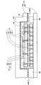
As a result, as shown in FIG. 5, the
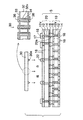
次いで、図6に示すように、下型42及び上型44から基本構成されるモールド金型40を用意する。そして、下型42の上に図5のインターポーザ付き配線基板6を配置する。さらに、下面側に凹部44xを備えた上型44をインターポーザ付き配線基板6の上に配置する。上型44の下面にはリリースフィルム46が設けられており、インターポーザ付き配線基板6のシリコンインターポーザ30の上面はリリースフィルム46で押えられた状態となる。リリースフィルム46は、シリコンインターポーザ30を保護すると共に、樹脂を充填した後に上型44を樹脂から容易に分離するための剥離層として機能する。
Next, as shown in FIG. 6, a
また、下型42の周縁部上にはインターポーザ付き配線基板6を取り囲むようにスペーサ48が配置されており、インターポーザ付き配線基板6の一辺の領域にはスペーサ48と上型44によって樹脂流入部Rが構成されている。また、樹脂流入部R以外の領域に配置されるスペーサ48は上型44の下に配置されたリリースフィルム46に接触しており、樹脂流入がそこでストップするようになっている。
A
このようにして、インターポーザ付き配線基板6を下型42と上型44とによって挟むことにより、樹脂流入部Rとそれに繋がって樹脂が充填される空間Aが構成される。樹脂が充填される空間Aは、第1ユニット配線板10と第2ユニット配線板20との隙間A1、第2ユニット配線板20とシリコンインターポーザ30との隙間A2、ベース配線板5の外周側面とモールド金型40との隙間A3、及びシリコンインターポーザ30の周辺の隙間A4である。
Thus, by sandwiching the interposer-equipped
次いで、同じく図6に示すように、溶融された樹脂を樹脂流入部Rを通してモールド金型40によって構成される空間Aに流し込む。このとき、空間Aを減圧して(又は真空にして)エアを排気した状態で樹脂が流入される。このようにして、樹脂が樹脂流入部Rからモールド金型40の中の空間Aに流入し、第1ユニット配線板10と第2ユニット配線板20との隙間A1及び第2ユニット配線板20とシリコンインターポーザ30との隙間A2などに樹脂が充填される。
Next, as shown in FIG. 6, the molten resin is poured into the space A constituted by the
さらに、空間Aに押し込まれた樹脂を熱処理して硬化させた後に、インターポーザ付き配線基板6からモールド金型40を取り外して樹脂を露出させる。このとき、上型44の下面にはリリースフィルム46が存在するので、上型44を樹脂から容易に取り外すことができる。その後に、樹脂流入部Rに形成された樹脂を折り取って廃棄する。
Further, after the resin pushed into the space A is cured by heat treatment, the molding die 40 is removed from the
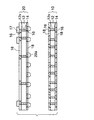
これにより、図7に示すように、第1ユニット配線板10と第2ユニット配線板20との隙間A1及び第2ユニット配線板20とシリコンインターポーザ30との隙間A2などに樹脂が充填されて、ベース配線板5とシリコンインターポーザ30とを一体化する樹脂部50が形成される。なお、第1ユニット配線板10と第2ユニット配線板20との隙間A1及び第2ユニット配線板20とシリコンインターポーザ30との隙間A2が比較的広い(100μm程度)場合は、空間Aを減圧することなく大気の状態で樹脂を充填することも可能である。
Thereby, as shown in FIG. 7, the gap A1 between the first
樹脂部50の材料としては、径が30μm程度以下のシリカフィラーが85〜90%含有されたエポキシ樹脂(モールドコンパウンド樹脂)が好適に使用され、その熱膨張係数は7〜20ppm/℃であり、弾性率は15〜25GPaである。樹脂部50はベース配線板5及びインターポーザ30を一体化する基板として機能し、上記した特性の樹脂材料を採用することにより、十分な剛性を有すると共に、後述するように反りの発生を抑制することができる。
As the material of the
また、一般的に、毛細管現象を利用して液状樹脂を隙間に充填する方法では、フィラーを多量に含む樹脂を狭い隙間に充填することは困難を極める。本実施形態では、第1ユニット配線板10と第2ユニット配線板20との隙間A1及び第2ユニット配線板20とシリコンインターポーザ30との隙間A2がかなり狭い(例えば30μm)場合であっても、真空トランスファモールド法によって樹脂を充填するので、フィラーを多量に含む樹脂を狭い隙間に信頼性よく充填することが可能である。
In general, in a method of filling a gap with a liquid resin using a capillary phenomenon, it is extremely difficult to fill a narrow gap with a resin containing a large amount of filler. In the present embodiment, even when the gap A1 between the first
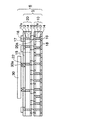
以上により、図7に示すように、本実施形態のインターポーザ内蔵配線基板7が得られる。図7に示すように、本実施形態のインターポーザ内蔵配線基板7では、第1ユニット配線板10の上に第2ユニット配線板20が厚さ方向に積層されて接続されてベース配線板5が構成されている。
As described above, as shown in FIG. 7, the interposer-embedded
第1ユニット配線板10では、絶縁層12の両面側に配線パターン16がそれぞれ形成されており、配線パターン16は絶縁層12のスルーホール12x内に充填されたスルーホール導電層14を介して相互接続されている。さらに、絶縁層12の両面側には配線パターン16の接続部上に開口部が設けられたソルダレジスト18がそれぞれ形成されている。
In the first
第2ユニット配線板20では、第1ユニット配線板10と同様に、絶縁層12の両面側にスルーホール導電層14を介して相互接続される配線パターン16がそれぞれ形成されている。また、絶縁層12の両面側には配線パターン16の接続部上に開口部が設けられたソルダレジスト18がそれぞれ形成されている。また、第2ユニット配線板20の上面の配線パターン16にキャパシタ部品17が接続されて実装されている。さらに、絶縁層12の下面側の配線パターン16の接続部に接続端子20aが設けられている。
In the second
そして、第1ユニット配線板10の配線パターン16の接続部に第2ユニット配線板20の接続端子20aが接合されて電気的に相互接続されている。
And the
さらに、ベース配線板5の上にシリコンインターポーザ30が厚さ方向に積層されて接続されている。シリコンインターポーザ30では、前述した図4で説明したように、シリコン基板32の両面側にスルーホール導電層34を介して相互接続される配線パターン36が形成され、その下面の配線パター36の接続部に金バンプなどからなる接続端子30aが設けられている。そして、シリコンインターポーザ30の接続端子30aがベース配線板5の配線パターン16の接続部にはんだ材22によって接合されている。
Further, a
さらに、第1ユニット配線板10と第2ユニット配線板20との隙間A1及び第2ユニット配線板20とシリコンインターポーザ30との隙間A2に樹脂部50が充填されている。樹脂部50はそれらの隙間A1,A2からベース配線板5及びシリコンインターポーザ30の側方にかけて繋がって一体的に形成されている。
Further, the
ベース配線板5及びシリコンインターポーザ30の側面は樹脂部50で被覆されていると共に、ベース配線板5の上に実装されたキャパシタ部品17が樹脂部50の中に埋設されている。シリコンインターポーザ30はその上面の半導体チップ搭載面が露出した状態で樹脂部50に埋設されており、シリコンインターポーザ30の上面と樹脂部50の上面が同一面となっている。
The side surfaces of the
このようにして、ベース配線板5及びシリコンインターポーザ30が樹脂部50によって一体化されており、樹脂部50はキャパシタ内蔵配線基板7の基板として機能する。図7には、外部接続方式をLGA(Land Grid Array)型として使用する例が示されており、ベース配線板5の下面の配線パターン16の接続部Cがランドとして使用される。
In this way, the
本実施形態では、樹脂部50の材料として、前述したように、反りの発生を防止するために熱膨張係数が7〜20ppm/℃の樹脂が使用される。シリコンインターポーザ30の熱膨張係数が3ppm/℃程度で、ベース配線板5の熱膨張係数が18ppm/℃程度であり、一般的な樹脂材料(熱膨張係数:40〜100ppm/℃)を使用する場合よりも、シリコンインターポーザ30、ベース配線板5及び樹脂部50の間で、熱膨張係数を近似させることができる。
In the present embodiment, as described above, a resin having a thermal expansion coefficient of 7 to 20 ppm / ° C. is used as a material for the
シリコンインターポーザ30、ベース配線板5及び樹脂部50の間で熱膨張係数が大きく異なる場合、樹脂を熱処理して硬化させる際などに熱膨張係数の差に基づく熱応力の発生によってインターポーザ内蔵配線基板7に反りが発生しやすい。反りが発生すると、後工程でのハンドリングに支障をきたしたり、実装基板(マザーボード)に実装する際にそれらの接合の信頼性が低下するなどの不具合が発生したりするおそれがある。
When the thermal expansion coefficients are greatly different among the
しかしながら、本実施形態では、上記したように、シリコンインターポーザ30、ベース配線板5及び樹脂部50の間で熱膨張係数が近似しているので、インターポーザ内蔵配線基板7の反りの発生を抑制することができ、信頼性を向上させることができる。
However, in this embodiment, as described above, since the thermal expansion coefficients are approximated among the
また、真空トランスファモールド法によって、第1ユニット配線板10と第2ユニット配線板20の隙間A1及び第2ユニット配線板20とシリコンインターポーザ30との隙間A2に樹脂が信頼性よく充填されて樹脂部50が形成される。しかも、樹脂部50は、高い弾性率を有する樹脂材料から形成されるので、ベース配線板5及びシリコンインターポーザ30を一体的に支持する剛性の高い基板として機能する。
Also, the resin is reliably filled in the gap A1 between the first
さらには、本実施形態では、絶縁層12の両面側に相互接続された配線パターン16が設けられた第1、第2ユニット配線板10,20を1ユニットとしてそれぞれ使用し、それらを積層することによりベース配線板5を構成している。
Furthermore, in the present embodiment, the first and second
このため、従来技術のビルドアップ配線板と違って、反りを防止するめにコア基板の両面に配線パターンを対称に形成する必要はなく、シリコンインターポーザ30の仕様に対応させて必要最小限の配線パターンの層数でベース配線板5を構成できる。従って、無駄な配線パターンを形成する必要がなくなるので、不必要な配線パターンの形成によるコスト上昇や歩留り低下を招くこともない。
Therefore, unlike the build-up wiring board of the prior art, it is not necessary to form wiring patterns symmetrically on both sides of the core substrate in order to prevent warping, and the minimum necessary wiring pattern corresponding to the specifications of the
なお、本実施形態では、第1ユニット配線板10と第2ユニット配線板20を積層してベース配線板5を構成したが、ユニット配線板の積層数は、設計仕様に合わせて第nユニット配線板(nは2以上の整数)まで任意に設定して積層することができる。
In this embodiment, the
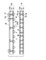
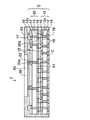
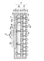
また、図8に示すシリコンインターポーザ内蔵基板7aのように、図7のインターポーザ内蔵配線基板7の下面側の配線パターン16の接続部Cにはんだボールなどを搭載して外部接続端子5aを設けてBGA(Ball Grid Array)型として使用してもよい。あるいは、PGA(Pin Grid Array)型として使用する場合は、インターポーザ内蔵配線基板7の下面側の配線パターン16の接続部Cにリードピンが設けられる。
Further, like the silicon interposer built-in
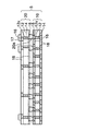
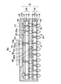
図9には、本実施形態の変形例のインターポーザ内蔵配線基板7bが示されている。変形例のインターポーザ内蔵配線基板7bでは、図8のインターポーザ内蔵配線基板7aの第1ユニット配線板10の上面の配線パターン16の接続部に半導体チップ60(LSIチップ)のバンプ60aがフリップチップ接続されており、半導体チップ60が樹脂部50の中に埋設されている。第1ユニット配線板10と半導体チップ60との間の隙間にも樹脂部50が充填されている。
FIG. 9 shows a
半導体チップ60は、第2ユニット配線板20の接続端子20aの高さによって構成される空間に収容され、樹脂部50で封止されている。第2ユニット配線板20の接続端子20aは、半導体チップ60の厚みに合わせて第1ユニット配線板10と第2ユニット配線板20との間に半導体チップ60が収容されるようにその高さが調整される。変形例のインターポーザ内蔵配線基板7bにおいても、前述したような真空トランスファモールド法によって樹脂部50が充填される。
The
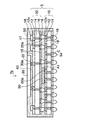
図10には本実施形態の半導体装置8が示されている。図8のインターポーザ内蔵配線基板7aのシリコンインターポーザ30の上面の配線パターン36(図4)の接続部に半導体チップ70(LSIチップ)のバンプ70aがフリップチップ接続されて実装されて、半導体装置8が構成される。ベース配線板5に実装されたキャパシタ部品17は半導体チップ70の電源ラインとグラウンドラインの間に接続されてデカップリングキャパシタとして機能する。
FIG. 10 shows the
半導体チップ70(シリコンチップ)は熱膨張係数が同一のシリコンインターポーザ30の上に実装されるので、半導体装置8の反りの発生を抑制することができる。なお、必要に応じて、シリコンインターポーザ30と半導体チップ70との隙間にアンダーフィル樹脂を充填してもよい。
Since the semiconductor chip 70 (silicon chip) is mounted on the
なお、1つの配線基板から複数の個々の配線基板を多面取りする場合は、半導体チップ70を実装する前又は後に、配線基板が切断される。
When a plurality of individual wiring boards are taken from one wiring board, the wiring board is cut before or after mounting the
その他の形態としては、ベース配線板5の上にシリコンインターポーザ30が実装された構造のユニットを2つ用意し、それらが対称になるように接続端子で接続することにより、配線基板の両面側にシリコンインターポーザが配置され、両面側に半導体チップが実装された形態としてもよい。この形態の場合、配線基板の下面周縁側の配線パターンに外部接続端子が接続される。
As another form, two units having a structure in which the
図11には、本発明の実施形態の変形例の半導体装置8aが示されている。図11に示すように、変形例の半導体装置8aでは、図9のインターポーザ内蔵配線基板7bのインターポーザ30に半導体チップ70のバンプ70aがフリップチップ接続されて構成される。
FIG. 11 shows a
本実施形態の半導体装置8,8aでは、狭小ピッチの接続電極を備えた高性能な半導体チップ70を実装する場合であっても、それに対応する微細な配線パターン36を備えたシリコンインターポーザ30の上に半導体チップ70を実装することにより、半導体チップ70の接続電極のピッチ変換を行ってベース配線板5に電気的に接続することができる。
In the
また、前述したように、本実施形態のベース配線板5は、シリコンインターポーザの仕様に合わせて必要最小限のユニット配線板を積層して構成できるので、半導体装置のコスト低減及び歩留りの向上と製造工程の簡略化を図ることができる。
Further, as described above, the
5…ベース配線板、6…インターポーザ付き配線基板、7,7a,7b…インターポーザ内蔵配線基板、8,8a…半導体装置、10…第1ユニット配線板、12,33…絶縁層、12x,32x…スルーホール、14,34…スルーホール導電層、16,36…配線パターン、17…キャパシタ部品、18…ソルダレジスト、20…第2ユニット配線板、20a,30a…接続端子、30…シリコンインターポーザ、32…シリコン基板、40…モールド金型、42…下型、44…上型、44x…凹部、46…リリースフィルム、48…スペーサ、50…樹脂部、60,70…半導体チップ、60a,70a…バンプ、A…空間、A1〜A4…隙間。
DESCRIPTION OF
Claims (10)
前記ベース配線板の上に積層され、上下側を導通可能にする配線パターンを備えて、前記ベース配線板の前記配線パターンに接続端子を介して接続されたシリコンインターポーザと、
前記複数のユニット配線板の間の隙間、及び前記ベース配線板と前記シリコンインターポーザとの隙間に充填され、前記ベース配線板及び前記シリコンインターポーザを一体化する樹脂部とを有することを特徴とする配線基板。 A plurality of unit wiring boards provided with wiring patterns that enable conduction on the upper and lower sides, and a base wiring board configured by being interconnected and stacked via connection terminals;
A silicon interposer that is laminated on the base wiring board and includes a wiring pattern that enables conduction on the upper and lower sides, and is connected to the wiring pattern of the base wiring board via a connection terminal;
A wiring board comprising: a gap between the plurality of unit wiring boards and a gap between the base wiring board and the silicon interposer, and a resin portion that integrates the base wiring board and the silicon interposer.
前記シリコンインターポーザの上面側の前記配線パターンに接続されて実装された半導体チップとを有することを特徴とする半導体装置。 The wiring board according to any one of claims 1 to 6,
And a semiconductor chip mounted on the wiring pattern on the upper surface side of the silicon interposer.
前記インターポーザ付き配線基板にモールド金型を設置し、真空トランスファモールド法によって、前記複数のユニット配線板の隙間、及び前記ベース配線板と前記シリコンインターポーザとの隙間に樹脂を充填することにより、前記ベース配線板及び前記シリコンインターポーザを一体化する樹脂部を形成する工程とを有することを特徴とする配線基板の製造方法。 A plurality of unit wiring boards with wiring patterns that allow conduction between the upper and lower sides are provided with a base wiring board configured by being interconnected and stacked via connection terminals, and a wiring pattern that allows conduction between the upper and lower sides. Preparing a silicon interposer, and connecting the silicon interposer to the wiring pattern of the base wiring board via a connection terminal to obtain a wiring board with an interposer;
The base is formed by installing a mold on the wiring board with the interposer and filling the gap between the plurality of unit wiring boards and the gap between the base wiring board and the silicon interposer by a vacuum transfer molding method. Forming a resin portion for integrating the wiring board and the silicon interposer.
Priority Applications (4)
| Application Number | Priority Date | Filing Date | Title |
|---|---|---|---|
| JP2006351000A JP4926692B2 (en) | 2006-12-27 | 2006-12-27 | WIRING BOARD, MANUFACTURING METHOD THEREOF, AND SEMICONDUCTOR DEVICE |
| TW096141679A TW200832673A (en) | 2006-12-27 | 2007-11-05 | Wiring substrate, manufacturing method thereof, and semiconductor device |
| US11/984,004 US7901986B2 (en) | 2006-12-27 | 2007-11-13 | Wiring substrate, manufacturing method thereof, and semiconductor device |
| CNA2007103011690A CN101211888A (en) | 2006-12-27 | 2007-12-26 | Wiring substrate, manufacturing method thereof, and semiconductor device |
Applications Claiming Priority (1)
| Application Number | Priority Date | Filing Date | Title |
|---|---|---|---|
| JP2006351000A JP4926692B2 (en) | 2006-12-27 | 2006-12-27 | WIRING BOARD, MANUFACTURING METHOD THEREOF, AND SEMICONDUCTOR DEVICE |
Publications (3)
| Publication Number | Publication Date |
|---|---|
| JP2008166327A true JP2008166327A (en) | 2008-07-17 |
| JP2008166327A5 JP2008166327A5 (en) | 2009-12-10 |
| JP4926692B2 JP4926692B2 (en) | 2012-05-09 |
Family
ID=39581929
Family Applications (1)
| Application Number | Title | Priority Date | Filing Date |
|---|---|---|---|
| JP2006351000A Active JP4926692B2 (en) | 2006-12-27 | 2006-12-27 | WIRING BOARD, MANUFACTURING METHOD THEREOF, AND SEMICONDUCTOR DEVICE |
Country Status (4)
| Country | Link |
|---|---|
| US (1) | US7901986B2 (en) |
| JP (1) | JP4926692B2 (en) |
| CN (1) | CN101211888A (en) |
| TW (1) | TW200832673A (en) |
Cited By (7)
| Publication number | Priority date | Publication date | Assignee | Title |
|---|---|---|---|---|
| JP2011114259A (en) * | 2009-11-30 | 2011-06-09 | Renesas Electronics Corp | Semiconductor device and method of manufacturing the same |
| KR20120087651A (en) * | 2011-01-28 | 2012-08-07 | 삼성전자주식회사 | Semiconductor device and fabricating method thereof |
| US8581394B2 (en) | 2010-06-21 | 2013-11-12 | Samsung Electro-Mechanics Co., Ltd | Semiconductor package module and electric circuit assembly with the same |
| CN104160284A (en) * | 2012-02-24 | 2014-11-19 | 罗伯特·博世有限公司 | Current sensor for fastening on a busbar |
| WO2015029951A1 (en) | 2013-08-26 | 2015-03-05 | 日立金属株式会社 | Mounting substrate wafer, multilayer ceramic substrate, mounting substrate, chip module, and mounting substrate wafer manufacturing method |
| JP2015090363A (en) * | 2013-11-04 | 2015-05-11 | ヴイアイエー・テクノロジーズ・インコーポレイテッド | Probe card |
| WO2017082416A1 (en) * | 2015-11-11 | 2017-05-18 | 京セラ株式会社 | Electronic component package |
Families Citing this family (36)
| Publication number | Priority date | Publication date | Assignee | Title |
|---|---|---|---|---|
| WO2009136495A1 (en) * | 2008-05-09 | 2009-11-12 | 国立大学法人九州工業大学 | Chip-size double side connection package and method for manufacturing the same |
| US20090277670A1 (en) * | 2008-05-10 | 2009-11-12 | Booth Jr Roger A | High Density Printed Circuit Board Interconnect and Method of Assembly |
| KR20100037300A (en) * | 2008-10-01 | 2010-04-09 | 삼성전자주식회사 | Method of forming semiconductor device having embedded interposer |
| WO2011033601A1 (en) * | 2009-09-21 | 2011-03-24 | 株式会社 東芝 | Method and apparatus for manufacturing three-dimensional integrated circuit |
| US8592973B2 (en) * | 2009-10-16 | 2013-11-26 | Stats Chippac Ltd. | Integrated circuit packaging system with package-on-package stacking and method of manufacture thereof |
| US9059187B2 (en) * | 2010-09-30 | 2015-06-16 | Ibiden Co., Ltd. | Electronic component having encapsulated wiring board and method for manufacturing the same |
| US20120292777A1 (en) * | 2011-05-18 | 2012-11-22 | Lotz Jonathan P | Backside Power Delivery Using Die Stacking |
| US20130154106A1 (en) | 2011-12-14 | 2013-06-20 | Broadcom Corporation | Stacked Packaging Using Reconstituted Wafers |
| US9548251B2 (en) | 2012-01-12 | 2017-01-17 | Broadcom Corporation | Semiconductor interposer having a cavity for intra-interposer die |
| US20130187284A1 (en) | 2012-01-24 | 2013-07-25 | Broadcom Corporation | Low Cost and High Performance Flip Chip Package |
| US8558395B2 (en) | 2012-02-21 | 2013-10-15 | Broadcom Corporation | Organic interface substrate having interposer with through-semiconductor vias |
| US8587132B2 (en) | 2012-02-21 | 2013-11-19 | Broadcom Corporation | Semiconductor package including an organic substrate and interposer having through-semiconductor vias |
| US8872321B2 (en) | 2012-02-24 | 2014-10-28 | Broadcom Corporation | Semiconductor packages with integrated heat spreaders |
| US8749072B2 (en) | 2012-02-24 | 2014-06-10 | Broadcom Corporation | Semiconductor package with integrated selectively conductive film interposer |
| US9275976B2 (en) | 2012-02-24 | 2016-03-01 | Broadcom Corporation | System-in-package with integrated socket |
| US8928128B2 (en) | 2012-02-27 | 2015-01-06 | Broadcom Corporation | Semiconductor package with integrated electromagnetic shielding |
| US9368458B2 (en) | 2013-07-10 | 2016-06-14 | Taiwan Semiconductor Manufacturing Company, Ltd. | Die-on-interposer assembly with dam structure and method of manufacturing the same |
| US12068231B2 (en) * | 2014-05-24 | 2024-08-20 | Broadpak Corporation | 3D integrations and methods of making thereof |
| JP2016058596A (en) * | 2014-09-11 | 2016-04-21 | ソニー株式会社 | Electronic device, component mounting substrate, and electronic equipment |
| TWI566305B (en) * | 2014-10-29 | 2017-01-11 | 巨擘科技股份有限公司 | Method for manufacturing three-dimensional integrated circuit |
| US10068181B1 (en) | 2015-04-27 | 2018-09-04 | Rigetti & Co, Inc. | Microwave integrated quantum circuits with cap wafer and methods for making the same |
| US9859202B2 (en) * | 2015-06-24 | 2018-01-02 | Dyi-chung Hu | Spacer connector |
| FR3044864B1 (en) * | 2015-12-02 | 2018-01-12 | Valeo Systemes De Controle Moteur | ELECTRIC DEVICE AND METHOD FOR ASSEMBLING SUCH AN ELECTRICAL DEVICE |
| US10181447B2 (en) | 2017-04-21 | 2019-01-15 | Invensas Corporation | 3D-interconnect |
| US10687419B2 (en) | 2017-06-13 | 2020-06-16 | Advanced Semiconductor Engineering, Inc. | Semiconductor package device and method of manufacturing the same |
| US11121301B1 (en) | 2017-06-19 | 2021-09-14 | Rigetti & Co, Inc. | Microwave integrated quantum circuits with cap wafers and their methods of manufacture |
| US10628354B2 (en) * | 2017-12-11 | 2020-04-21 | Micron Technology, Inc. | Translation system for finer grain memory architectures |
| KR102661196B1 (en) * | 2019-11-08 | 2024-04-29 | 삼성전자 주식회사 | Electronic device including stacked printed circuit board |
| US11515173B2 (en) * | 2019-12-27 | 2022-11-29 | Taiwan Semiconductor Manufacturing Company, Ltd. | Semiconductor devices and methods of manufacturing |
| CN113053758A (en) | 2019-12-27 | 2021-06-29 | 台湾积体电路制造股份有限公司 | Method for manufacturing semiconductor device |
| US20220069489A1 (en) * | 2020-08-28 | 2022-03-03 | Unimicron Technology Corp. | Circuit board structure and manufacturing method thereof |
| US11540396B2 (en) * | 2020-08-28 | 2022-12-27 | Unimicron Technology Corp. | Circuit board structure and manufacturing method thereof |
| CN111933590B (en) * | 2020-09-11 | 2021-01-01 | 甬矽电子(宁波)股份有限公司 | Packaging structure and manufacturing method thereof |
| CN113270327B (en) * | 2021-07-20 | 2021-12-07 | 珠海越亚半导体股份有限公司 | Active and passive device vertical laminated embedded packaging structure and manufacturing method thereof |
| US12040284B2 (en) | 2021-11-12 | 2024-07-16 | Invensas Llc | 3D-interconnect with electromagnetic interference (“EMI”) shield and/or antenna |
| CN116825746A (en) * | 2023-07-03 | 2023-09-29 | 武汉新芯集成电路制造有限公司 | Semiconductor packaging structure and manufacturing method thereof |
Citations (4)
| Publication number | Priority date | Publication date | Assignee | Title |
|---|---|---|---|---|
| JP2002222901A (en) * | 2001-01-29 | 2002-08-09 | Sony Corp | Semiconductor device mounting method and mounting structure, semiconductor device manufacturing method, and semiconductor device |
| JP2005039232A (en) * | 2003-06-24 | 2005-02-10 | Ngk Spark Plug Co Ltd | Relay board with semiconductor element, board with relay board, structure comprising semiconductor element, relay board and substrate |
| JP2005340389A (en) * | 2004-05-25 | 2005-12-08 | Renesas Technology Corp | Semiconductor device and manufacturing method thereof |
| JP2006286677A (en) * | 2005-03-31 | 2006-10-19 | Renesas Technology Corp | Semiconductor device and manufacturing method thereof |
Family Cites Families (10)
| Publication number | Priority date | Publication date | Assignee | Title |
|---|---|---|---|---|
| TW434756B (en) * | 1998-06-01 | 2001-05-16 | Hitachi Ltd | Semiconductor device and its manufacturing method |
| JP2001102479A (en) | 1999-09-27 | 2001-04-13 | Toshiba Corp | Semiconductor integrated circuit device and method of manufacturing the same |
| JP3679786B2 (en) * | 2002-06-25 | 2005-08-03 | 松下電器産業株式会社 | Manufacturing method of semiconductor device |
| JP4390541B2 (en) * | 2003-02-03 | 2009-12-24 | Necエレクトロニクス株式会社 | Semiconductor device and manufacturing method thereof |
| JP3917946B2 (en) | 2003-03-11 | 2007-05-23 | 富士通株式会社 | Multilayer semiconductor device |
| TW200726784A (en) * | 2003-04-07 | 2007-07-16 | Hitachi Chemical Co Ltd | Epoxy resin molding material for sealing use and semiconductor device |
| JP4205613B2 (en) * | 2004-03-01 | 2009-01-07 | エルピーダメモリ株式会社 | Semiconductor device |
| US7105918B2 (en) * | 2004-07-29 | 2006-09-12 | Micron Technology, Inc. | Interposer with flexible solder pad elements and methods of manufacturing the same |
| JP2007036104A (en) * | 2005-07-29 | 2007-02-08 | Nec Electronics Corp | Semiconductor device and manufacturing method thereof |
| US7608921B2 (en) * | 2006-12-07 | 2009-10-27 | Stats Chippac, Inc. | Multi-layer semiconductor package |
-
2006
- 2006-12-27 JP JP2006351000A patent/JP4926692B2/en active Active
-
2007
- 2007-11-05 TW TW096141679A patent/TW200832673A/en unknown
- 2007-11-13 US US11/984,004 patent/US7901986B2/en active Active
- 2007-12-26 CN CNA2007103011690A patent/CN101211888A/en active Pending
Patent Citations (4)
| Publication number | Priority date | Publication date | Assignee | Title |
|---|---|---|---|---|
| JP2002222901A (en) * | 2001-01-29 | 2002-08-09 | Sony Corp | Semiconductor device mounting method and mounting structure, semiconductor device manufacturing method, and semiconductor device |
| JP2005039232A (en) * | 2003-06-24 | 2005-02-10 | Ngk Spark Plug Co Ltd | Relay board with semiconductor element, board with relay board, structure comprising semiconductor element, relay board and substrate |
| JP2005340389A (en) * | 2004-05-25 | 2005-12-08 | Renesas Technology Corp | Semiconductor device and manufacturing method thereof |
| JP2006286677A (en) * | 2005-03-31 | 2006-10-19 | Renesas Technology Corp | Semiconductor device and manufacturing method thereof |
Cited By (10)
| Publication number | Priority date | Publication date | Assignee | Title |
|---|---|---|---|---|
| JP2011114259A (en) * | 2009-11-30 | 2011-06-09 | Renesas Electronics Corp | Semiconductor device and method of manufacturing the same |
| US8763242B2 (en) | 2009-11-30 | 2014-07-01 | Renesas Electronics Corporation | Semiconductor device and method of manufacturing the same |
| US8581394B2 (en) | 2010-06-21 | 2013-11-12 | Samsung Electro-Mechanics Co., Ltd | Semiconductor package module and electric circuit assembly with the same |
| KR20120087651A (en) * | 2011-01-28 | 2012-08-07 | 삼성전자주식회사 | Semiconductor device and fabricating method thereof |
| JP2012160707A (en) * | 2011-01-28 | 2012-08-23 | Samsung Electronics Co Ltd | Multilayer semiconductor chip, semiconductor device, and manufacturing method for these |
| KR101719636B1 (en) * | 2011-01-28 | 2017-04-05 | 삼성전자 주식회사 | Semiconductor device and fabricating method thereof |
| CN104160284A (en) * | 2012-02-24 | 2014-11-19 | 罗伯特·博世有限公司 | Current sensor for fastening on a busbar |
| WO2015029951A1 (en) | 2013-08-26 | 2015-03-05 | 日立金属株式会社 | Mounting substrate wafer, multilayer ceramic substrate, mounting substrate, chip module, and mounting substrate wafer manufacturing method |
| JP2015090363A (en) * | 2013-11-04 | 2015-05-11 | ヴイアイエー・テクノロジーズ・インコーポレイテッド | Probe card |
| WO2017082416A1 (en) * | 2015-11-11 | 2017-05-18 | 京セラ株式会社 | Electronic component package |
Also Published As
| Publication number | Publication date |
|---|---|
| JP4926692B2 (en) | 2012-05-09 |
| US20080155820A1 (en) | 2008-07-03 |
| TW200832673A (en) | 2008-08-01 |
| US7901986B2 (en) | 2011-03-08 |
| CN101211888A (en) | 2008-07-02 |
Similar Documents
| Publication | Publication Date | Title |
|---|---|---|
| JP4926692B2 (en) | WIRING BOARD, MANUFACTURING METHOD THEREOF, AND SEMICONDUCTOR DEVICE | |
| JP5079475B2 (en) | Electronic component mounting package | |
| JP6325605B2 (en) | Electronic component built-in substrate | |
| JP5389770B2 (en) | Printed circuit board with built-in electronic element and manufacturing method thereof | |
| TWI479971B (en) | Wiring board, manufacturing method thereof, and semiconductor device having wiring board | |
| CN105637633B (en) | Embedded package with preformed vias | |
| US9716075B2 (en) | Semiconductor chip assembly and method for making same | |
| CN104428892B (en) | Method and apparatus for substrate core layer | |
| JP2017123459A (en) | Printed circuit board | |
| JP2010034403A (en) | Wiring substrate and electronic component device | |
| JP2009194322A (en) | Semiconductor device manufacturing method, semiconductor device, and wiring board | |
| CN110729254B (en) | Bonding structure of package and manufacturing method thereof | |
| TW201318129A (en) | Package substrate with embedded perforation interposer and preparation method thereof | |
| JP2011142286A (en) | Electronic component-embedded printed circuit board, and method of manufacturing the same | |
| US9324580B2 (en) | Process for fabricating a circuit substrate | |
| JP2009117767A (en) | Semiconductor device manufacturing method and semiconductor device manufactured thereby | |
| JP2010239126A (en) | Semiconductor device and manufacturing method of semiconductor device | |
| JP2011071315A (en) | Wiring board and method of manufacturing the same | |
| JP2000138453A (en) | Wiring board | |
| US20160353576A1 (en) | Electronic component built-in substrate and electronic device | |
| JP2009081357A (en) | Wiring board manufacturing method and wiring board | |
| CN100433321C (en) | Circuit board and circuit device using the same | |
| JP5174355B2 (en) | WIRING BOARD, MANUFACTURING METHOD THEREOF, AND SEMICONDUCTOR DEVICE | |
| CN1560911B (en) | Manufacturing method of circuit carrier plate | |
| US12341088B2 (en) | Wiring board and semiconductor device each having non-photosensitive thermosetting encapsulating layer over photosensitive resin layer of interconnect structure |
Legal Events
| Date | Code | Title | Description |
|---|---|---|---|
| A521 | Request for written amendment filed |
Free format text: JAPANESE INTERMEDIATE CODE: A523 Effective date: 20091023 |
|
| A621 | Written request for application examination |
Free format text: JAPANESE INTERMEDIATE CODE: A621 Effective date: 20091023 |
|
| A977 | Report on retrieval |
Free format text: JAPANESE INTERMEDIATE CODE: A971007 Effective date: 20100301 |
|
| TRDD | Decision of grant or rejection written | ||
| A01 | Written decision to grant a patent or to grant a registration (utility model) |
Free format text: JAPANESE INTERMEDIATE CODE: A01 Effective date: 20120207 |
|
| A01 | Written decision to grant a patent or to grant a registration (utility model) |
Free format text: JAPANESE INTERMEDIATE CODE: A01 |
|
| A61 | First payment of annual fees (during grant procedure) |
Free format text: JAPANESE INTERMEDIATE CODE: A61 Effective date: 20120208 |
|
| FPAY | Renewal fee payment (event date is renewal date of database) |
Free format text: PAYMENT UNTIL: 20150217 Year of fee payment: 3 |
|
| R150 | Certificate of patent or registration of utility model |
Ref document number: 4926692 Country of ref document: JP Free format text: JAPANESE INTERMEDIATE CODE: R150 Free format text: JAPANESE INTERMEDIATE CODE: R150 |