JP5174355B2 - WIRING BOARD, MANUFACTURING METHOD THEREOF, AND SEMICONDUCTOR DEVICE - Google Patents
WIRING BOARD, MANUFACTURING METHOD THEREOF, AND SEMICONDUCTOR DEVICE Download PDFInfo
- Publication number
- JP5174355B2 JP5174355B2 JP2007024228A JP2007024228A JP5174355B2 JP 5174355 B2 JP5174355 B2 JP 5174355B2 JP 2007024228 A JP2007024228 A JP 2007024228A JP 2007024228 A JP2007024228 A JP 2007024228A JP 5174355 B2 JP5174355 B2 JP 5174355B2
- Authority
- JP
- Japan
- Prior art keywords
- wiring board
- unit
- substrate
- unit wiring
- wiring pattern
- Prior art date
- Legal status (The legal status is an assumption and is not a legal conclusion. Google has not performed a legal analysis and makes no representation as to the accuracy of the status listed.)
- Active
Links
Images


Classifications
-
- H—ELECTRICITY
- H01—ELECTRIC ELEMENTS
- H01L—SEMICONDUCTOR DEVICES NOT COVERED BY CLASS H10
- H01L2224/00—Indexing scheme for arrangements for connecting or disconnecting semiconductor or solid-state bodies and methods related thereto as covered by H01L24/00
- H01L2224/01—Means for bonding being attached to, or being formed on, the surface to be connected, e.g. chip-to-package, die-attach, "first-level" interconnects; Manufacturing methods related thereto
- H01L2224/10—Bump connectors; Manufacturing methods related thereto
- H01L2224/15—Structure, shape, material or disposition of the bump connectors after the connecting process
- H01L2224/16—Structure, shape, material or disposition of the bump connectors after the connecting process of an individual bump connector
- H01L2224/161—Disposition
- H01L2224/16151—Disposition the bump connector connecting between a semiconductor or solid-state body and an item not being a semiconductor or solid-state body, e.g. chip-to-substrate, chip-to-passive
- H01L2224/16221—Disposition the bump connector connecting between a semiconductor or solid-state body and an item not being a semiconductor or solid-state body, e.g. chip-to-substrate, chip-to-passive the body and the item being stacked
- H01L2224/16225—Disposition the bump connector connecting between a semiconductor or solid-state body and an item not being a semiconductor or solid-state body, e.g. chip-to-substrate, chip-to-passive the body and the item being stacked the item being non-metallic, e.g. insulating substrate with or without metallisation
-
- H—ELECTRICITY
- H01—ELECTRIC ELEMENTS
- H01L—SEMICONDUCTOR DEVICES NOT COVERED BY CLASS H10
- H01L2224/00—Indexing scheme for arrangements for connecting or disconnecting semiconductor or solid-state bodies and methods related thereto as covered by H01L24/00
- H01L2224/01—Means for bonding being attached to, or being formed on, the surface to be connected, e.g. chip-to-package, die-attach, "first-level" interconnects; Manufacturing methods related thereto
- H01L2224/42—Wire connectors; Manufacturing methods related thereto
- H01L2224/47—Structure, shape, material or disposition of the wire connectors after the connecting process
- H01L2224/49—Structure, shape, material or disposition of the wire connectors after the connecting process of a plurality of wire connectors
- H01L2224/491—Disposition
- H01L2224/4912—Layout
- H01L2224/49175—Parallel arrangements
-
- H—ELECTRICITY
- H01—ELECTRIC ELEMENTS
- H01L—SEMICONDUCTOR DEVICES NOT COVERED BY CLASS H10
- H01L2924/00—Indexing scheme for arrangements or methods for connecting or disconnecting semiconductor or solid-state bodies as covered by H01L24/00
- H01L2924/15—Details of package parts other than the semiconductor or other solid state devices to be connected
- H01L2924/151—Die mounting substrate
- H01L2924/153—Connection portion
- H01L2924/1531—Connection portion the connection portion being formed only on the surface of the substrate opposite to the die mounting surface
- H01L2924/15311—Connection portion the connection portion being formed only on the surface of the substrate opposite to the die mounting surface being a ball array, e.g. BGA
-
- H—ELECTRICITY
- H01—ELECTRIC ELEMENTS
- H01L—SEMICONDUCTOR DEVICES NOT COVERED BY CLASS H10
- H01L2924/00—Indexing scheme for arrangements or methods for connecting or disconnecting semiconductor or solid-state bodies as covered by H01L24/00
- H01L2924/15—Details of package parts other than the semiconductor or other solid state devices to be connected
- H01L2924/181—Encapsulation
Landscapes
- Production Of Multi-Layered Print Wiring Board (AREA)
Description
本発明は配線基板及びその製造方法と半導体装置に係り、さらに詳しくは、半導体チップが実装される多層配線を有する配線基板及びその製造方法と半導体装置に関する。 The present invention relates to a wiring board, a manufacturing method thereof, and a semiconductor device, and more particularly to a wiring board having a multilayer wiring on which a semiconductor chip is mounted, a manufacturing method thereof, and a semiconductor device.
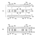
従来、CPUなどの半導体チップが配線基板の上に実装されて構成される半導体装置がある。半導体チップを実装するための配線基板としては、配線が多層化されて形成されたビルドアップ配線板が一般的に使用されている。 Conventionally, there is a semiconductor device configured by mounting a semiconductor chip such as a CPU on a wiring board. As a wiring board for mounting a semiconductor chip, a build-up wiring board formed by multilayering wiring is generally used.
図1に示すように、従来技術のビルドアップ配線板では、コア基板100にスルーホールTHが設けられており、そのスルーホールTHの内面にスルーホールめっき層120が形成されている。コア基板100の両面にはスルーホールめっき層120を介して相互接続された第1配線パターン200がそれぞれ形成されている。スルーホールTHの孔は樹脂140で埋め込まれている。
As shown in FIG. 1, in the conventional build-up wiring board, a through hole TH is provided in the
また、コア基板100の両面側には、第1配線パターン200を被覆する層間絶縁層300がそれぞれ形成されており、層間絶縁層300には第1配線パターン200に到達する深さのビアホールVHがそれぞれ形成されている。
In addition, an
さらに、コア基板100の両面側の層間絶縁層300の上には、ビアホールVHを介して第1配線パターン200に接続される第2配線パターン220がそれぞれ形成されている。
Furthermore,
このように、従来技術のビルドアップ配線板では、コア基板100の両面側にセミアディティブ法などによって配線パターンが繰り返し形成されて相互接続された所要の多層配線が形成される。
As described above, in the conventional build-up wiring board, a required multilayer wiring is formed by repeatedly forming a wiring pattern on both sides of the
そのような配線基板に関連する技術としては、特許文献1には、半導体チップ内の配線層数を減らすために半導体チップ内の配線の機能をインターポーザに移し、配線基板の上にインターポーザを介して半導体チップを実装することが記載されている。 As a technique related to such a wiring board, Patent Document 1 discloses that the function of wiring in the semiconductor chip is transferred to the interposer in order to reduce the number of wiring layers in the semiconductor chip, and the interposer is placed on the wiring board via the interposer. It is described that a semiconductor chip is mounted.
また、特許文献2には、外部接続端子を備えた第1の配線基板に半導体素子が実装された上部装置部と、接続用電極を備えた第2の配線基板に半導体素子が実装された下部装置部との間に、インターポーザ基板を配設することが記載されている。
ところで、近年では半導体チップの高性能化に伴って配線基板の配線パターンのさらなるファインピッチ化や多層化が要求されている。図1に示した従来技術のビルドアップ配線板では、半導体チップの高性能化に対応させて配線パターンのさらなる多層化を行うとき、片面側の配線パターンの追加のみで対応できる場合であっても、反りの発生を防止するためにコア基板の両面側に配線パターンを対称に形成する必要があり、無駄なコストがかかる問題がある。 Incidentally, in recent years, with higher performance of semiconductor chips, further fine pitches and multilayers of wiring patterns on wiring boards are required. In the prior art build-up wiring board shown in FIG. 1, when the wiring pattern is further multi-layered in response to the higher performance of the semiconductor chip, even if only the addition of the wiring pattern on one side is possible. In order to prevent the occurrence of warping, it is necessary to form wiring patterns symmetrically on both sides of the core substrate, and there is a problem that wasteful cost is required.
特に、CPUなどの高性能な半導体チップが実装される配線基板では、厚膜化が要求される電源ラインやグランドラインが多く、形成に手間がかかる配線パターンの層数が膨大になるケースが想定され、コスト上昇や歩留りの低下が懸念される。 In particular, in a wiring board on which a high-performance semiconductor chip such as a CPU is mounted, there are many power supply lines and ground lines that are required to be thick, and the number of wiring pattern layers that take time to form becomes enormous. Therefore, there are concerns about an increase in cost and a decrease in yield.
本発明は以上の課題を鑑みて創作されたものであり、製造工程が簡略化されて低コスト・高歩留りで製造される信頼性の高い配線基板及びその製造方法と半導体装置を提供することを目的とする。 The present invention was created in view of the above problems, and provides a highly reliable wiring board manufactured at a low cost and with a high yield by simplifying the manufacturing process, a manufacturing method thereof, and a semiconductor device. Objective.
上記課題を解決するため、本発明は配線基板に係り、基板と、前記基板の少なくとも上面に形成され、垂直方向に立設する層間接続部が一体的に設けられた第1配線パターンとにより構成される第1ユニット配線板と、前記第1ユニット配線板の上に形成され、上下側を導通可能にする第2配線パターンを備えた第2ユニット配線板と、前記第1ユニット配線板と前記第2ユニット配線板の間に充填された樹脂部とを有し、前記第1配線パターンは電源プレーン及びグランドプレーンを含み、前記第2配線パターンは前記第1ユニット配線板の前記層間接続部に接続され、前記第1配線パターン及びそれに繋がって立設する前記層間接続部は、リードフレームが加工されて一体的に形成され、前記第1配線パターンの厚みは前記第2配線パターンの厚みより厚いことを特徴とする。 In order to solve the above-mentioned problems, the present invention relates to a wiring board, and includes a board and a first wiring pattern that is formed on at least the upper surface of the board and is integrally provided with an interlayer connection portion standing in a vertical direction. A first unit wiring board, a second unit wiring board formed on the first unit wiring board, and having a second wiring pattern that allows conduction on the upper and lower sides; the first unit wiring board; A resin portion filled between the second unit wiring boards, wherein the first wiring pattern includes a power plane and a ground plane, and the second wiring pattern is connected to the interlayer connection portion of the first unit wiring board. The first wiring pattern and the inter-layer connection portion standing upright connected thereto are integrally formed by processing a lead frame, and the thickness of the first wiring pattern is the second wiring pattern. And wherein the thicker than the emissions of thickness.
本発明の配線基板では、基板の少なくとも上面にリードフレームから形成された第1配線パターンが接着されており、第1配線パターンはそれと一体的に形成されて垂直方向に立設する層間接続部を備えている。そして、基板と第1配線パターンとにより第1ユニット配線板が構成されている。 In the wiring board of the present invention, the first wiring pattern formed from the lead frame is bonded to at least the upper surface of the board, and the first wiring pattern is formed integrally therewith and has an interlayer connection portion standing vertically. I have. A first unit wiring board is constituted by the substrate and the first wiring pattern.
また、第1ユニット配線板の上には、上下側を導通可能にする第2配線パターンを備えた第2ユニット配線板が配置されており、第2ユニット配線板の第2配線パターンが第1ユニット配線板の層間接続部に接続されている。 Further, on the first unit wiring board, a second unit wiring board having a second wiring pattern that allows conduction between the upper and lower sides is disposed, and the second wiring pattern of the second unit wiring board is the first. It is connected to the interlayer connection part of the unit wiring board.
さらに、第1ユニット配線板と第2ユニット配線板の間に樹脂部が充填されており、樹脂部は第1、第2ユニット配線板を一体化する基板として機能すると共に、第1、第2ユニット配線板を絶縁する層間絶縁部として機能する。 Further, a resin part is filled between the first unit wiring board and the second unit wiring board, and the resin part functions as a substrate for integrating the first and second unit wiring boards, and the first and second unit wirings. It functions as an interlayer insulation that insulates the plate.
本発明の配線基板では、厚みの厚いリードフレームから形成された第1配線パターンを備えた第1ユニット配線板の上に第2ユニット配線板50が積層されて多層配線構造を構成している。このため、従来技術のような銅箔やめっきによって配線を形成する場合よりも、低コストで容易に厚膜(例えば100μm以上)の電源プレーンやグランドプレーンを形成することができる。これにより、配線基板の電源プレーンやグランドプレーンの低抵抗化を図ることで電源系を強化することができ、高性能な半導体チップ搭載用の配線基板として対応できるようになる。
In the wiring board of the present invention, a second
また、従来技術の基板上に配線を順次作り込んでいくビルドアップ配線板の製造方法と違って、ユニット配線板を積層し、その間に樹脂を充填して配線基板を構成するので、短手番で配線基板を製造することができ、製造効率を向上させることができる。しかも、良品のユニット配線板を選別して多層化できるので、従来技術よりも製造歩留りを格段に向上させることができる。 Also, unlike the build-up wiring board manufacturing method in which wiring is sequentially built on the substrate of the prior art, the unit wiring board is stacked and filled with resin between them to configure the wiring board. Thus, the wiring board can be manufactured, and the manufacturing efficiency can be improved. In addition, since a good unit wiring board can be selected and multi-layered, the manufacturing yield can be significantly improved as compared with the prior art.
また、本発明の好適な態様では、樹脂部として、フィラーが85〜90%含有された樹脂を使用することにより、半導体チップ(シリコンLSIチップ)の熱膨張係数に近似させることができると共に、基板の強度を向上させることができる。これにより、配線基板に半導体チップを実装して半導体装置を構成する際に、高い信頼性が得られるようになる。 Further, in a preferred aspect of the present invention, the resin portion can be approximated to the thermal expansion coefficient of a semiconductor chip (silicon LSI chip) by using a resin containing 85 to 90% filler, and the substrate. The strength of can be improved. Accordingly, high reliability can be obtained when a semiconductor device is configured by mounting a semiconductor chip on a wiring board.
上記した発明において、第1ユニット配線板の基板が貫通電極を備えており、第1ユニット配線板が、基板の両面側に、貫通電極を介して相互接続された前記第1配線パターンがそれぞれ形成されて構成されるようにしてもよい。この態様では、第2ユニット配線板が第1ユニット配線板の両面側の第1配線パターンの層間接続部にそれぞれ接続されて配置され、樹脂部は、第1ユニット配線板と、その両面側に配置された第2ユニット配線板との間にそれぞれ充填される。 In the above-described invention, the substrate of the first unit wiring board includes a through electrode, and the first unit wiring board is formed on each side of the substrate with the first wiring pattern interconnected through the through electrode. And may be configured. In this aspect, the second unit wiring board is disposed and connected to the interlayer connection portion of the first wiring pattern on both sides of the first unit wiring board, and the resin portion is provided on the first unit wiring board and on both sides thereof. Each is filled between the arranged second unit wiring boards.
上記課題を解決するため、本発明は配線基板の製造方法に係り、基板と、垂直方向に立設する層間接続部が設けられて、連結部によって相互に繋がって形成された第1配線パターンを備えたリードフレームとを用意する工程と、前記基板の少なくとも上面に、前記第1配線パターンの前記層間接続部が外側に配置されるように前記リードフレームを接着する工程と、前記リードフレームの前記連結部を除去して前記第1配線パターンを相互に分離することにより、前記基板と前記第1配線パターンにより構成される第1ユニット配線板を得る工程と、上下側を導通可能にする第2配線パターンを備えた第2ユニット配線板を用意し、前記第1ユニット配線板の前記第1配線パターンの前記層間接続部に、前記第2ユニット配線板の前記第2配線パターンを接続する工程と、真空トランスファモールド法によって、前記第1ユニット配線板と前記第2ユニット配線板の間に樹脂を充填することにより、前記第1ユニット配線板及び前記第2ユニット配線板を一体化する樹脂部を形成する工程とを有し、前記リードフレームを用意する工程は、金属薄板の上に形成されたマスク材をマスクにして、前記金属薄板を厚みの途中までウェットエッチングすることにより前記層間接続部を形成する工程と、前記層間接続部を形成する工程の前又は後に、前記金属薄板を貫通加工することにより前記第1配線パターンを形成する工程とを含むことを特徴とする。 In order to solve the above-mentioned problems, the present invention relates to a method of manufacturing a wiring board, and includes a first wiring pattern formed by connecting a board and an interlayer connection part standing in a vertical direction and interconnecting them by a connecting part. Preparing a lead frame provided, adhering the lead frame so that the interlayer connection portion of the first wiring pattern is disposed on at least the upper surface of the substrate, and the lead frame A step of obtaining a first unit wiring board constituted by the substrate and the first wiring pattern by removing the connecting portion and separating the first wiring patterns from each other; A second unit wiring board provided with a wiring pattern is prepared, and the second wiring of the second unit wiring board is disposed on the interlayer connection portion of the first wiring pattern of the first unit wiring board. The first unit wiring board and the second unit wiring board are integrated by filling a resin between the first unit wiring board and the second unit wiring board by a pattern connecting step and a vacuum transfer molding method. Forming the resin part, and the step of preparing the lead frame is performed by wet etching the metal thin plate halfway through the thickness using the mask material formed on the metal thin plate as a mask. The method includes a step of forming an interlayer connection portion and a step of forming the first wiring pattern by penetrating the thin metal plate before or after the step of forming the interlayer connection portion .
本発明の配線基板の製造方法を使用することにより、上記した配線基板を容易に製造することができる。 By using the method for manufacturing a wiring board according to the present invention, the above-described wiring board can be easily manufactured.
本発明の好適な態様では、リードフレームが接着される基板はプリプレグから形成され、プリプレグが硬化して基板になる際の接着作用によってリードフレームが基板に固着される。また、真空トランスファモールド法によって第1、第2ユニット配線板の間に樹脂を充填するので、それらの隙間が狭い場合であってもフィラーを多量に含む樹脂を信頼性よく充填することができる。 In a preferred aspect of the present invention, the substrate to which the lead frame is bonded is formed from a prepreg, and the lead frame is fixed to the substrate by an adhesive action when the prepreg is cured to become a substrate. In addition, since the resin is filled between the first and second unit wiring boards by the vacuum transfer molding method, the resin containing a large amount of filler can be filled with high reliability even when the gap between them is narrow.
以上説明したように、本発明の配線基板は、製造工程が簡略化されて低コスト・高歩留りで製造される。 As described above, the wiring board of the present invention is manufactured at a low cost and a high yield by simplifying the manufacturing process.
以下、本発明の実施の形態について、添付の図面を参照して説明する。 Hereinafter, embodiments of the present invention will be described with reference to the accompanying drawings.
(第1の実施の形態)
図2〜図8は本発明の第1実施形態の配線基板の製造方法を示す断面図、図9は本発明の第1実施形態の配線基板を示す断面図、図10は同じく半導体装置を示す断面図である。
(First embodiment)
2 to 8 are cross-sectional views showing a method for manufacturing a wiring board according to the first embodiment of the present invention, FIG. 9 is a cross-sectional view showing the wiring board according to the first embodiment of the present invention, and FIG. 10 similarly shows a semiconductor device. It is sectional drawing.
本実施形態の配線基板の製造方法では、図2(a)に示すように、まず、リードフレームを製造するための厚みが100〜200μmの銅合金材からなる金属薄板10を用意する。金属薄板10の材料としては銅合金や銅が好適に使用される。さらに、金属薄板10の上にレジスト19(マスク材)をフォトリソグラフィによってパターニングする。レジスト19は、金属薄板10上の層間接続部が形成される部分に配置される。
In the method for manufacturing a wiring board according to the present embodiment, as shown in FIG. 2A, first, a metal
続いて、レジスト19をマスクにして、塩化第二鉄水溶液又は塩化第二銅水溶液を使用するウェットエッチングにより、金属薄膜10を厚みの途中までエッチングする。その後に、レジスト19が除去される。
Subsequently, using the
これにより、図2(b)に示すように、金属薄板10に繋がって垂直方向に立設する電源ライン用の層間接続部12a、グランドライン用の層間接続部14a及び信号ライン用の層間接続部16aが形成される。各層間接続部12a,14a,16aの高さは例えば30〜50μmに設定され、それらの径が0.5mm程度(ピッチ:1mm程度)の設計ルールで形成することが可能である。
As a result, as shown in FIG. 2B, the power supply line
次いで、図2(c)に示すように、金型を使用するプレス加工によって層間接続部12a、14a,16aが設けられた金属薄板10を打ち抜くことにより、電源プレーン12、グランドプレーン14及び信号線パッド16が画定されてリードフレーム20が得られる。
Next, as shown in FIG. 2 (c), the metal
このとき、電源プレーン12、グランドプレーン14及び信号線パッド16は連結部18によって繋がった状態となって画定され、グランドプレーン14はリードフレーム20の枠部としても機能する。
At this time, the
またこのとき、電源プレーン12、グランドプレーン14及び信号線パッド16は、それらに繋がって立設する電源ライン用の層間接続部12a、グランドライン用の層間接続部14a及び信号ライン用の層間接続部16aがそれぞれ設けられた状態となる。
At this time, the
なお、層間接続部12a、14a,16aが設けられた金属薄板10の上にレジストをパターニングした後に、金属薄板をウェットエッチングにより貫通加工することにより、電源プレーン12、グランドプレーン14及び信号線パッド16を形成してもよい。
In addition, after patterning a resist on the
金属薄板10は長尺状に引き出された状態で加工され、層間接続部12a,14a、16aがそれぞれ設けられた電源プレーン12、グランドプレーン14及び信号線パッド16を備えたリードフレーム20が順次形成される。そして、個々のリードフレーム20が得られるように金属薄板10が切断される。
The metal
後に説明するように、リードフレーム20の連結部18が除去されることにより、電源プレーン12、グランドプレーン14及び信号線パッド16が独立した正規の配線となる。なお、金属薄板10をプレス加工して電源プレーン12、グランドプレーン14及び信号線パッド16を画定した後に、金属薄板10を厚みの途中までエッチングして層間接続部12a,14a、16aを形成してもよい。
As will be described later, by removing the connecting
次いで、図3(a)に示すように、ガラスクロスやアラミド繊維などにエポキシ樹脂などの樹脂を含侵させたプリプレグ(prepreg)30aを用意する。プリプレグ30aはB−ステージ(半硬化状態)のものが使用される。さらに、プリプレグ30aにスルーホールTHを形成し、スルーホールTHの中にめっき被膜を形成するか又は導電性ペーストを埋め込むなどして貫通電極32を形成する。
Next, as shown in FIG. 3A, a
続いて、同じく図3(a)に示すように、前述した図2(c)で作成した2枚のリードフレーム20を用意し、プリプレグ30aの両面側にリードフレーム20をそれぞれ配置する。各リードフレーム20は、プリプレグ30aの外側に層間接続部12a、14a,16aが立設するようにしてそれぞれ配置される。
Subsequently, as shown in FIG. 3A, the two
さらに、リードフレーム20を加熱した状態でプリプレグ30a側に押圧することにより(熱プレス)、プレプレグ30aを硬化させると共に、2枚のリードフレーム20をプレプレグ30aの両面にそれぞれ接着させる。
Further, by pressing the
このようにして、図3(b)に示すように、プレプレグ30aが硬化することによりコア基板30が得られる。プレプレグ30aは硬化するときに接着機能を有するので、接着剤を特別に使用することなく、コア基板30の両面側にリードフレーム20がそれぞれ固着される。
In this way, as shown in FIG. 3B, the
次いで、図4(a)に示すように、リードフレーム20の連結部18(図2(c)参照)を除去することにより、電源プレーン12、グランドプレーン14及び信号線パッド16が独立して相互に電気絶縁された状態とする。つまり、図3(b)のコア基板30の両面側のリードフレーム20の連結部18の上に開口部が設けられたレジスト(不図示)がそれぞれ形成された後に、レジストの開口部の連結部18がウェットエッチングにより除去される。リードフレーム20は、コア基板30に接着されているので、連結部18を除去しても、電源プレーン12、グランドプレーン14及び信号線パッド16はコア基板30の両面に固定された状態で残される。
Next, as shown in FIG. 4A, the connecting portion 18 (see FIG. 2C) of the
このようにして、図4(b)に示すように、コア基板30の両面側に、正規の配線として機能する電源プレーン12、グランドプレーン14及び信号線パッド16から構成される第1配線パターンW1が形成される。コア基板30の両面側の電源プレーン12は、コア基板30内の電源ライン用の貫通電極32を介して相互接続される。また、同様に、コア基板30の両面側のグランドプレーン14は、コア基板30内のグランドライン用の貫通電極32を介して相互接続される。また、同様に、コア基板30の両面側の信号線パッド16は、コア基板30内の信号ライン用の貫通電極32を介して相互接続される。
In this way, as shown in FIG. 4B, on the both sides of the
以上により、コア基板30の両面側に、リードフレーム20から形成された第1配線パターンW1がそれぞれ形成された構造の第1ユニット配線板40が得られる。
As described above, the first
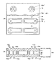
次いで、図5に示すように、2枚の第2ユニット配線板50を用意する。図5の上図に示すように、第2ユニット配線板50では、プリプレグなどから形成された絶縁性の基板52に貫通電極54が設けられており、基板52の両面側に貫通電極54を介して相互接続された第2配線パターンW2がそれぞれ形成されている。基板52の上面には第2配線パターンW2の接続部上に開口部が設けられたソルダレジスト56が形成されている。図5の下図には上図の第2ユニット配線板50が上下左右反転したものが示されている。
Next, as shown in FIG. 5, two second
第2ユニット配線板50は半導体チップが実装されるものであり、その第2配線パターンW2は、第1ユニット配線板50の第1配線パターンW1より薄膜(例えば30μm程度)でかつファインピッチで形成される。このような観点から、第2ユニット配線板50の絶縁性の基板52の代わりにシリコン基板を使用し、第2ユニット配線板50が上下側を導通可能するより微細な配線パターンを両面に備えたシリコンインターポーザから構成されるようにしてもよい。
The second
続いて、図6に示すように、2枚の第2ユニット配線板50のソルダレジスト56が設けられていない側の第2配線パターンW2に導電性ペースト59をそれぞれ塗布する。さらに、2枚の第2ユニット配線板50の導電性ペースト59が設けられた第2配線パターンW2を第1ユニット配線板40の両面側の電源プレーン12、グランドプレーン14及び信号線パッド16の各層間接続部12a,14a,16aに導電性ペースト59を介してそれぞれ接合する。
Subsequently, as shown in FIG. 6, a
これにより、図7に示すように、第1ユニット配線板40の両面側の層間接続部12a,14a,16aに第2ユニット配線板50の配線パターン56がそれぞれ接続された構造の配線立体構造体5が得られる。この配線立体構造体5では、コア基板30の両面側において、第1ユニット配線板40の電源プレーン12、グランドプレーン14及び信号線パッド16(第1配線パターンW1)はそれらの層間接続部12a,14a、16aを介して第2ユニット配線板50の電源ライン用、グランドライン用及び信号ライン用の第2配線パターンW2にそれぞれ接続される。そして、コア基板30の両面側の第1、第2配線パターンW1,W2は、コア基板30の貫通電極32を介してそれぞれ相互接続される。
As a result, as shown in FIG. 7, a wiring three-dimensional structure having a structure in which the
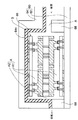
次いで、図8に示すように、下型62及び上型64から基本構成されるモールド金型60を用意する。そして、下型62の上に図7の配線立体構造体5を配置する。
Next, as shown in FIG. 8, a
さらに、下面側に凹部64xを備えた上型64を配線立体構造体5の上に配置する。上型64の下面にはリリースフィルム66が設けられており、配線立体構造体5の上面はリリースフィルム66で押えられた状態となる。リリースフィルム66は、配線立体構造体5を保護すると共に、樹脂を充填した後に上型64を樹脂から容易に分離するための剥離層として機能する。
Furthermore, an
また、下型62の周縁部上には配線立体構造体5を取り囲むようにスペーサ68が配置されており、配線立体構造体5の一辺の領域にはスペーサ68と上型64によって樹脂流入部Rが構成されている。また、樹脂流入部R以外の領域に配置されるスペーサ68は上型64の下に配置されたリリースフィルム66に接触しており、樹脂流入がそこでストップするようになっている。なお、下型62の表面(配線立体構造体5との当接面)にもリリースフィルムを介在させてもよい。
A
このようにして、配線立体構造体5を下型62と上型64とによって挟むことにより、樹脂流入部Rとそれに繋がって樹脂が充填される空間Aが構成される。樹脂が充填される空間Aは、第1ユニット配線板40と第2ユニット配線板50の隙間A1と、配線立体構造体5の外面と金型60との隙間A2などである。
In this way, by sandwiching the wiring three-
次いで、同じく図8に示すように、溶融された樹脂を樹脂流入部Rを通してモールド金型60によって構成される空間Aに流し込む。このとき、空間Aを減圧して(又は真空にして)エアを排気した状態で樹脂が流入される。このようにして、樹脂が樹脂流入部Rからモールド金型60の中の空間Aに流入し、第1ユニット配線板40と第2ユニット配線板50の隙間A1と、配線立体構造体5の外側の隙間A2などに樹脂が充填される。
Next, similarly as shown in FIG. 8, the melted resin is poured into the space A constituted by the
さらに、空間Aに押し込まれた樹脂を熱処理して硬化させた後に、配線立体構造体5からモールド金型60を取り外して樹脂を露出させる。このとき、上型64の下面にはリリースフィルム66が存在するので、上型64を樹脂から容易に取り外すことができる。その後に、樹脂流入部Rに形成された樹脂を折り取って廃棄する。
Furthermore, after the resin pushed into the space A is cured by heat treatment, the
これにより、図9に示すように、第1ユニット配線板40と第2ユニット配線板50の隙間A1に樹脂が充填されて、第1、第2ユニット配線板40,50を一体化する樹脂部70が形成される。なお、第1ユニット配線板40と第2ユニット配線板50隙間A1が比較的広い(100μm程度)場合は、空間Aを減圧することなく大気の状態で樹脂を充填することも可能である。
As a result, as shown in FIG. 9, the resin is filled in the gap A1 between the first
樹脂部70の材料としては、径が30μm程度以下のシリカフィラーが85〜90%含有されたエポキシ樹脂(モールドコンパウンド樹脂)が好適に使用され、その熱膨張係数は7〜20ppm/℃であり、弾性率は15〜25GPaである。樹脂部70は第1、第4ユニット配線板40,50を一体化する基板として機能し、上記した特性の樹脂材料を採用することにより、十分な剛性を有すると共に、後述するように反りの発生を抑制することができる。
As the material of the
また、一般的に、毛細管現象を利用して液状樹脂を隙間に充填する方法では、フィラーを多量に含む樹脂を狭い隙間に充填することは困難を極める。本実施形態では、第1ユニット配線板40と第2ユニット配線板50の隙間A1がかなり狭い(例えば30μm)場合であっても、真空トランスファモールド法によって樹脂を充填するので、フィラーを多量に含む樹脂を狭い隙間に信頼性よく充填することが可能である。
In general, in a method of filling a gap with a liquid resin using a capillary phenomenon, it is extremely difficult to fill a narrow gap with a resin containing a large amount of filler. In the present embodiment, even when the gap A1 between the first
以上により、本実施形態の配線基板1が得られる。 The wiring board 1 of this embodiment is obtained by the above.
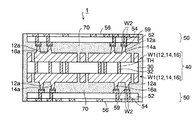
図9に示すように、本実施形態の配線基板1では、第1ユニット配線板40の両面側に第2ユニット配線板50がそれぞれ接続され、第1ユニット配線板40と第2ユニット配線板50の間に樹脂部70が充填されて基本構成される。
As shown in FIG. 9, in the wiring board 1 of the present embodiment, the second
第1ユニット配線板40では、コア基板30に貫通電極32が設けられており、コア基板30の両面側に貫通電極32を介して相互接続された第1配線パターンW1がそれぞれ接着されている。第1配線パターンW1は、リードフレーム20から形成され、電源プレーン12、グランドプレーン14及び信号線パッド16(図4(a)参照)から構成されている。そして、コア基板30の両面側の電源プレーン12、グランドプレーン14,及び信号線パッド16には、それらと一体的に形成されて垂直方向(コア基板30の外側)に立設する層間接続部12a,14a、16aがそれぞれ設けられている。
In the first
また、第2ユニット配線基板50では、絶縁性の基板52に貫通電極54が設けられており、基板52の両面側には貫通電極54を介して相互接続された第2配線パターンW2がそれぞれ形成されている。さらに、第1ユニット配線板40の両面側に配置された第2ユニット配線基板50の各外面には、第2配線パターンW2の接続部上に開口部が設けられたソルダレジスト56が形成されている。第2ユニット配線板50の第2配線パターンW2の積層数はn層(nは2以上の整数)で任意に設定することができる。
Further, in the second
第1ユニット配線板40の両面側において、第1ユニット配線板40の電源プレーン12の層間接続部12a、グランドプレーン14の層間接続部14a及び信号線パッド16の層間接続部16aに、導電性ペースト59によって第2ユニット配線板50の第2配線パターンW2の電源ライン、グランドライン及び信号ラインがそれぞれ接続されている。
On both sides of the first
このようにして、コア基板30の両面側の電源ライン(電源プレーン12とそれに接続された第2配線パターンW2)がコア基板30の貫通電極32を介して相互接続されている。また同様に、コア基板30の両面側のグランドライン(グランドプレーン12とそれに接続された第2配線パターンW2)がコア基板30の貫通電極32を介して相互接続されている。また同様に、コア基板30の両面側の信号ライン(信号線パッド16とそれに接続された第2配線パターンW2)がコア基板30の貫通電極32を介して相互接続されている。
In this way, the power supply lines (the
さらに、第1ユニット配線板40と第2ユニット配線板50の間には樹脂部70が充填されている。第1、第2ユニット配線板40,50は樹脂部70によって一体化されており、樹脂部70は配線基板1の基板として機能すると共に、第1、第2ユニット配線板40,50を絶縁する層間絶縁部として機能する。
Further, a
そして、図10に示すように、本実施形態の配線基板1では、上側の第2ユニット配線板50の第2配線パターンW2に半導体チップ80(シリコンLSIチップ)のバンプ80aがフリップチップ接続される。さらに、下側の第2ユニット配線板50の第2配線パターンW2にはんだボールが搭載されるなどして外部接続端子72が設けられる。以上により、本実施形態の半導体装置2が構成される。
As shown in FIG. 10, in the wiring board 1 of the present embodiment, the
外部接続方式をBGA(Ball Grid Array)型とする例を示したが、LGA(Land Grid Array)型とする場合は、外部接続端子72が省略されて最下の第2配線パターンW2の接続部がランドとして使用される。あるいは、PGA(Pin Grid Array)型として使用する場合は、最下の第2配線パターンW2の接続部にリードピンが設けられる。
Although an example in which the external connection method is the BGA (Ball Grid Array) type has been shown, in the case of the LGA (Land Grid Array) type, the
なお、第1ユニット配線板40のコア基板30の片面のみに第1配線パターンW1とそれに接続される第2ユニット配線板50が形成された形態としてもよい。この場合、コア基板30の貫通電極32の下面に外部接続端子が設けられる。
The first wiring pattern W1 and the second
本実施形態では、樹脂部70の材料として、前述したように、反りの発生を防止するために熱膨張係数が7〜20ppm/℃の樹脂が使用される。半導体チップ80(シリコンLSIチップ)の熱膨張係数が3ppm/℃程度であり、一般的な樹脂材料(熱膨張係数:40〜100ppm/℃)を使用する場合よりも、半導体チップ80と配線基板1との間で熱膨張係数を近似させることができる。これにより、半導体チップを配線基板に実装する際に反りの発生を抑制できるので、半導体装置の信頼性を向上させることができる。
In the present embodiment, as described above, a resin having a thermal expansion coefficient of 7 to 20 ppm / ° C. is used as a material for the
また、真空トランスファモールド法によって、第1ユニット配線板40と第2ユニット配線板50の隙間A1に樹脂が信頼性よく充填されて樹脂部70が形成される。しかも、樹脂部70は、高い弾性率を有する樹脂材料から形成されるので、第1、2ユニット配線板40,50を一体的に支持する剛性の高い基板として機能する。
Further, the
さらには、本実施形態では、層間接続部12a,14a,16aがそれぞれ立設する電源プレーン12、グランドプレーン14及び信号線パッド16を厚みの厚いリードフレーム20から形成し、その上に第2ユニット配線板50を積層して配線基板1を構成している。これにより、従来技術のような銅箔やめっきによって配線を形成する場合よりも、低コストで容易に第2ユニット配線板50の第2配線パターンW2よりもかなり厚い(100μm以上)の電源プレーン12やグランドプレーン14を形成することができる。
Further, in the present embodiment, the
従って、配線基板1の電源プレーン12やグランドプレーン14の低抵抗化を図ることで電源系を強化することができ、高性能な半導体チップ搭載用の配線基板として対応できるようになる。
Therefore, by reducing the resistance of the
また、従来技術の基板上に配線を順次作り込んでいくビルドアップ配線板の製造方法と違って、ユニット配線板を積層し、その間に樹脂を充填して配線基板を構成するので、短手番で配線基板を製造することができ、製造効率を向上させることができる。しかも、良品のユニット配線板を選別して多層化できるので、従来技術(ビルドアップ配線板)よりも製造歩留りを格段に向上させることができる。 Also, unlike the build-up wiring board manufacturing method in which wiring is sequentially built on the substrate of the prior art, the unit wiring board is stacked and filled with resin between them to configure the wiring board. Thus, the wiring board can be manufactured, and the manufacturing efficiency can be improved. In addition, since a good unit wiring board can be selected and multilayered, the manufacturing yield can be remarkably improved as compared with the prior art (build-up wiring board).
(第2の実施の形態)
図11は本発明の第2実施形態の半導体装置を示す断面図、図12は本発明の第2実施形態に係るリードフレームから形成された第1配線パターンに半導体チップが接続されて実装された様子を示す平面図である。
(Second Embodiment)
FIG. 11 is a cross-sectional view showing a semiconductor device according to the second embodiment of the present invention, and FIG. 12 shows a semiconductor chip connected to the first wiring pattern formed from the lead frame according to the second embodiment of the present invention. It is a top view which shows a mode.
第2実施形態の特徴は、リードフレームから形成された第1配線パターンに電子部品を実装して配線基板の内部に電子部品を内蔵させることにある。第2実施形態では、第1実施形態と同一要素については、同一符号を付してその説明を省略する。 A feature of the second embodiment is that an electronic component is mounted on a first wiring pattern formed from a lead frame, and the electronic component is built in the wiring board. In the second embodiment, the same elements as those in the first embodiment are denoted by the same reference numerals and description thereof is omitted.
図11及び図12に示すように、第2実施形態の半導体装置2aでは、配線基板1の第1ユニット配線板40の第1配線パターンW1は、電源プレーン12、グランドプレーン14、信号配線16x及びダイパッド17から構成される。そして、電源プレーン12、グランドプレーン14及び信号配線16xには、それらに繋がって立設する電源ライン用の層間接続部12a、グランドライン用の層間接続部14a及び信号ライン用の層間接続部16aがそれぞれ設けられている。第2実施形態では、信号配線16xが第1実施形態の信号線パッド16として機能する共に、半導体チップがワイヤボンディングされるリードとして機能する。
As shown in FIGS. 11 and 12, in the
第2実施形態では、第1実施形態と同様に、まず、金属薄板10が加工されて、層間接続部12a,14a,16aがそれぞれ立設した電源プレーン12、グランドプレーン14及び信号配線16xと、ダイパッド17とが連結部で繋がったリードフレームが形成される。さらに、そのリードフレームがコア基板30の両面に接着された後に、連結部がエッチングされて除去される。これにより、図12に示すように、相互に電気絶縁された電源プレーン12、グランドプレーン14、信号配線16x及びダイパッド17がコア基板30の両面に形成される。
In the second embodiment, as in the first embodiment, first, the metal
そして、同じく図12に示すように、ダイパッド17の上に半導体チップ81がフェイスアップで固着され、ワイヤボンディング法によるワイヤ83によって半導体チップ81の接続パッドが電源プレーン12、グランドプレーン14及び信号配線16xに接続される。図12には、半導体チップ81がワイヤ83で信号配線16xに接続された部分が示されている。
Similarly, as shown in FIG. 12, the
コア基板20の下面側のダイパッド17上にも半導体チップ81が実装され、同様に半導体チップ81の接続パッドがワイヤ83によって信号配線16xなどに接続される。
The
これにより、半導体チップ81が両面側に実装された第1ユニット配線板40が得られる。続いて、第1実施形態と同様に、第1ユニット配線板40の両面の各層間接続部12a,14a、16aに第2ユニット配線板50の第2配線パターンW2を導電性ペースト59を介してそれぞれ接続する。
Thereby, the 1st
さらに、第1ユニット配線板40と第2ユニット配線板50の間に樹脂部70が充填されることで半導体チップ81が封止される。これにより、半導体チップ81が内蔵された配線基板1aが得られる。なお、配線基板1aに内蔵される電子部品としては、半導体チップ81の他にキャパシタや抵抗などの受動素子があり、半導体チップ81及び受動部品のいずれか又は両方を第1ユニット配線板40と第2ユニット配線板50の間に実装し、樹脂部70で埋設してもよい。
Furthermore, the
さらに、第1実施形態と同様に、配線基板1の上面の第2配線パターンW2に半導体チップ80のバンプ80aがフリップチップ接続され、下面の第2配線パターンW2に外部接続端子72が設けられる。これにより、第2実施形態の半導体装置2aが得られる。
Further, as in the first embodiment, the
第2実施形態の半導体装置2aは第1実施形態と同様な効果を奏する。これに加えて、第1、第2ユニット配線板40,50の間に半導体チップや受動部品を内蔵させるようにしたので、より高性能な半導体装置を構成することができる。
The
1,1a…配線基板、2,2a…半導体装置、10…金属薄板、12…電源プレーン、12a,14a,16a…層間接続部、14…グランドプレーン、16…信号線パッド、16x…信号配線、18…連結部、20…リードフレーム、30…コア基板、30a…プリプレグ、32,54…貫通電極、40…第1ユニット配線板、50…第2ユニット配線板、52…基板、56…ソルダレジスト、60…モールド金型、62…下型、64…上型、64x…凹部、66…リリースフィルム、68…スペーサ、70…樹脂部、72…外部接続端子、80,81…半導体チップ、80a…バンプ、83…ワイヤ、A…空間、A1,A2…隙間、W1…第1配線パターン、W2…第2配線パターン、R…樹脂流入部。
DESCRIPTION OF
Claims (8)
前記第1ユニット配線板の上に形成され、上下側を導通可能にする第2配線パターンを備えた第2ユニット配線板と、
前記第1ユニット配線板と前記第2ユニット配線板の間に充填された樹脂部とを有し、
前記第1配線パターンは電源プレーン及びグランドプレーンを含み、前記第2配線パターンは前記第1ユニット配線板の前記層間接続部に接続され、
前記第1配線パターン及びそれに繋がって立設する前記層間接続部は、リードフレームが加工されて一体的に形成され、前記第1配線パターンの厚みは前記第2配線パターンの厚みより厚いことを特徴とする配線基板。 A first unit wiring board composed of a substrate and a first wiring pattern formed on at least the upper surface of the substrate and integrally provided with an interlayer connection portion standing in the vertical direction;
A second unit wiring board that is formed on the first unit wiring board and includes a second wiring pattern that allows conduction between the upper and lower sides;
A resin portion filled between the first unit wiring board and the second unit wiring board;
The first wiring pattern includes a power plane and a ground plane, and the second wiring pattern is connected to the interlayer connection portion of the first unit wiring board.
The first wiring pattern and the inter-layer connection portion erected in connection with the first wiring pattern are integrally formed by processing a lead frame, and the thickness of the first wiring pattern is thicker than the thickness of the second wiring pattern. Wiring board.
前記第1ユニット配線板は、前記基板の両面側に、前記貫通電極に接続されて外側に前記層間接続部が立設した前記第1配線パターンがそれぞれ形成されて構成され、
前記第2ユニット配線板が前記第1ユニット配線板の両面側の第1配線パターンの前記層間接続部にそれぞれ接続されて配置されており、
前記樹脂部は、前記第1ユニット配線板とその両面側に配置された前記第2ユニット配線板との間にそれぞれ充填されていることを特徴とする請求項1に記載の配線基板。 The substrate of the first unit wiring board includes a through electrode;
The first unit wiring board is formed by forming the first wiring patterns on both sides of the substrate, the first wiring patterns being connected to the through electrodes and having the interlayer connection portions standing on the outside.
The second unit wiring board is connected to the interlayer connection portion of the first wiring pattern on both sides of the first unit wiring board, and is disposed.
2. The wiring board according to claim 1, wherein the resin portion is filled between the first unit wiring board and the second unit wiring boards disposed on both sides thereof.
前記配線基板における前記第2ユニット配線板の外面側の前記第2配線パターンにフリップチップ接続された半導体チップとを有することを特徴とする半導体装置。 The wiring board according to claim 1 or 2,
And a semiconductor chip flip-chip connected to the second wiring pattern on the outer surface side of the second unit wiring board in the wiring board.
前記基板の少なくとも上面に、前記第1配線パターンの前記層間接続部が外側に配置されるように前記リードフレームを接着する工程と、
前記リードフレームの前記連結部を除去して前記第1配線パターンを相互に分離することにより、前記基板と前記第1配線パターンにより構成される第1ユニット配線板を得る工程と、
上下側を導通可能にする第2配線パターンを備えた第2ユニット配線板を用意し、前記第1ユニット配線板の前記第1配線パターンの前記層間接続部に、前記第2ユニット配線板の前記第2配線パターンを接続する工程と、
真空トランスファモールド法によって、前記第1ユニット配線板と前記第2ユニット配線板の間に樹脂を充填することにより、前記第1ユニット配線板及び前記第2ユニット配線板を一体化する樹脂部を形成する工程とを有し、
前記リードフレームを用意する工程は、
金属薄板の上に形成されたマスク材をマスクにして、前記金属薄板を厚みの途中までウェットエッチングすることにより前記層間接続部を形成する工程と、
前記層間接続部を形成する工程の前又は後に、前記金属薄板を貫通加工することにより前記第1配線パターンを形成する工程とを含むことを特徴とする配線基板の製造方法。 Preparing a substrate and a lead frame provided with a first wiring pattern provided with an interlayer connection portion standing in the vertical direction and interconnected by a connecting portion;
Bonding the lead frame such that the interlayer connection portion of the first wiring pattern is disposed outside at least on the upper surface of the substrate;
Removing the connecting portion of the lead frame and separating the first wiring patterns from each other to obtain a first unit wiring board constituted by the substrate and the first wiring pattern;
A second unit wiring board having a second wiring pattern that allows conduction on the upper and lower sides is prepared, and the interlayer connection portion of the first wiring pattern of the first unit wiring board is provided with the second unit wiring board. Connecting the second wiring pattern;
Forming a resin portion for integrating the first unit wiring board and the second unit wiring board by filling a resin between the first unit wiring board and the second unit wiring board by a vacuum transfer molding method; It has a door,
The step of preparing the lead frame includes
Using the mask material formed on the metal thin plate as a mask, forming the interlayer connection portion by wet etching the metal thin plate halfway through the thickness;
And a step of forming the first wiring pattern by penetrating the thin metal plate before or after the step of forming the interlayer connection portion .
前記リードフレームを前記基板に接着する工程において、前記プリプレグを熱処理して硬化させることによって前記基板を得ると共に、前記基板の上に前記リードフレームを接着させることを特徴とする請求項5に記載の配線基板の製造方法。 In the step of preparing the substrate, the substrate comprises a semi-cured prepreg,
6. The step of bonding the lead frame to the substrate, wherein the substrate is obtained by heat-treating and curing the prepreg, and the lead frame is bonded on the substrate. A method for manufacturing a wiring board.
前記リードフレームを前記基板に接着する工程において、前記基板の両面側に、前記貫通電極に接続される前記リードフレームをそれぞれ接着し、
第1ユニット配線板を得る工程、及び前記第2ユニット配線板を前記第1ユニット配線板に接続する工程は、前記基板の両面側で行われ、
前記樹脂部は、前記第1ユニット配線板とその両面側に配置された前記第2ユニット配線板の間に充填されることを特徴とする請求項5に記載の配線基板の製造方法。 The substrate includes a through electrode;
In the step of bonding the lead frame to the substrate, each of the lead frames connected to the through electrode is bonded to both sides of the substrate,
The step of obtaining the first unit wiring board and the step of connecting the second unit wiring board to the first unit wiring board are performed on both sides of the substrate,
6. The method of manufacturing a wiring board according to claim 5, wherein the resin portion is filled between the first unit wiring board and the second unit wiring boards arranged on both sides thereof.
樹脂部を形成する工程において、前記電子部品が樹脂部に埋設されることを特徴とする請求項5に記載の配線基板の製造方法。 After the step of obtaining the first unit wiring board, the method further comprises a step of connecting and mounting electronic components on the first unit wiring board to the first wiring pattern,
6. The method of manufacturing a wiring board according to claim 5, wherein in the step of forming the resin portion, the electronic component is embedded in the resin portion.
Priority Applications (1)
| Application Number | Priority Date | Filing Date | Title |
|---|---|---|---|
| JP2007024228A JP5174355B2 (en) | 2007-02-02 | 2007-02-02 | WIRING BOARD, MANUFACTURING METHOD THEREOF, AND SEMICONDUCTOR DEVICE |
Applications Claiming Priority (1)
| Application Number | Priority Date | Filing Date | Title |
|---|---|---|---|
| JP2007024228A JP5174355B2 (en) | 2007-02-02 | 2007-02-02 | WIRING BOARD, MANUFACTURING METHOD THEREOF, AND SEMICONDUCTOR DEVICE |
Publications (3)
| Publication Number | Publication Date |
|---|---|
| JP2008192740A JP2008192740A (en) | 2008-08-21 |
| JP2008192740A5 JP2008192740A5 (en) | 2010-02-12 |
| JP5174355B2 true JP5174355B2 (en) | 2013-04-03 |
Family
ID=39752576
Family Applications (1)
| Application Number | Title | Priority Date | Filing Date |
|---|---|---|---|
| JP2007024228A Active JP5174355B2 (en) | 2007-02-02 | 2007-02-02 | WIRING BOARD, MANUFACTURING METHOD THEREOF, AND SEMICONDUCTOR DEVICE |
Country Status (1)
| Country | Link |
|---|---|
| JP (1) | JP5174355B2 (en) |
Families Citing this family (3)
| Publication number | Priority date | Publication date | Assignee | Title |
|---|---|---|---|---|
| JP5577760B2 (en) * | 2009-03-09 | 2014-08-27 | 新光電気工業株式会社 | Package substrate and method for manufacturing semiconductor device |
| US11244874B2 (en) * | 2018-03-16 | 2022-02-08 | Mitsubishi Electric Corporation | Substrate bonding structure and substrate bonding method |
| JP2023006236A (en) * | 2021-06-30 | 2023-01-18 | 株式会社オートネットワーク技術研究所 | Circuit structure and electric connection box |
Family Cites Families (4)
| Publication number | Priority date | Publication date | Assignee | Title |
|---|---|---|---|---|
| JPH0383396A (en) * | 1989-08-28 | 1991-04-09 | Fujitsu Ltd | Multilayer printed circuit board |
| JPH08181417A (en) * | 1994-12-26 | 1996-07-12 | Furukawa Electric Co Ltd:The | Manufacture of circuit material |
| JP3553043B2 (en) * | 2001-01-19 | 2004-08-11 | 松下電器産業株式会社 | Component built-in module and manufacturing method thereof |
| JP2004014679A (en) * | 2002-06-05 | 2004-01-15 | Fcm Kk | Circuit board for lamination, and laminated circuit |
-
2007
- 2007-02-02 JP JP2007024228A patent/JP5174355B2/en active Active
Also Published As
| Publication number | Publication date |
|---|---|
| JP2008192740A (en) | 2008-08-21 |
Similar Documents
| Publication | Publication Date | Title |
|---|---|---|
| JP4926692B2 (en) | WIRING BOARD, MANUFACTURING METHOD THEREOF, AND SEMICONDUCTOR DEVICE | |
| JP4055717B2 (en) | Semiconductor device and manufacturing method thereof | |
| JP5711472B2 (en) | WIRING BOARD, MANUFACTURING METHOD THEREOF, AND SEMICONDUCTOR DEVICE | |
| JP6539992B2 (en) | Printed circuit board, semiconductor device, method of manufacturing wired circuit board, method of manufacturing semiconductor device | |
| US9232657B2 (en) | Wiring substrate and manufacturing method of wiring substrate | |
| JP4298559B2 (en) | Electronic component mounting structure and manufacturing method thereof | |
| JP5395360B2 (en) | Manufacturing method of electronic component built-in substrate | |
| US7705446B2 (en) | Package structure having semiconductor chip embedded therein and method for fabricating the same | |
| JP5389770B2 (en) | Printed circuit board with built-in electronic element and manufacturing method thereof | |
| KR101119303B1 (en) | A printed circuit board comprising embedded electronic component within and a method for manufacturing the same | |
| KR102107037B1 (en) | Printed circuit board and method of manufacturing the same | |
| US20140151876A1 (en) | Semiconductor package and process for fabricating same | |
| US9313894B2 (en) | Wiring substrate and manufacturing method of wiring substrate | |
| JP4730426B2 (en) | Mounting substrate and semiconductor module | |
| KR20160091050A (en) | A printed circuit board comprising embeded electronic component within and a method for manufacturing | |
| JPWO2007126090A1 (en) | CIRCUIT BOARD, ELECTRONIC DEVICE DEVICE, AND CIRCUIT BOARD MANUFACTURING METHOD | |
| JP2010034403A (en) | Wiring substrate and electronic component device | |
| JP2015106615A (en) | Printed wiring board and method for manufacturing printed wiring board | |
| JP2008028376A (en) | Circuit board, semiconductor module and method of manufacturing circuit board | |
| JP5406572B2 (en) | Electronic component built-in wiring board and manufacturing method thereof | |
| JP2017108019A (en) | Wiring board, semiconductor package, semiconductor device, method for manufacturing wiring board and method for manufacturing semiconductor package | |
| JP2009252942A (en) | Component built-in wiring board, and method of manufacturing component built-in wiring board | |
| JP5174355B2 (en) | WIRING BOARD, MANUFACTURING METHOD THEREOF, AND SEMICONDUCTOR DEVICE | |
| JP4438389B2 (en) | Manufacturing method of semiconductor device | |
| JP2008182163A (en) | Wiring substrate and manufacturing method therefor, and semiconductor device |
Legal Events
| Date | Code | Title | Description |
|---|---|---|---|
| A521 | Written amendment |
Free format text: JAPANESE INTERMEDIATE CODE: A523 Effective date: 20091216 |
|
| A621 | Written request for application examination |
Free format text: JAPANESE INTERMEDIATE CODE: A621 Effective date: 20091216 |
|
| A977 | Report on retrieval |
Free format text: JAPANESE INTERMEDIATE CODE: A971007 Effective date: 20111007 |
|
| A131 | Notification of reasons for refusal |
Free format text: JAPANESE INTERMEDIATE CODE: A131 Effective date: 20111025 |
|
| A521 | Written amendment |
Free format text: JAPANESE INTERMEDIATE CODE: A523 Effective date: 20111213 |
|
| A131 | Notification of reasons for refusal |
Free format text: JAPANESE INTERMEDIATE CODE: A131 Effective date: 20120612 |
|
| A521 | Written amendment |
Free format text: JAPANESE INTERMEDIATE CODE: A523 Effective date: 20120726 |
|
| TRDD | Decision of grant or rejection written | ||
| A01 | Written decision to grant a patent or to grant a registration (utility model) |
Free format text: JAPANESE INTERMEDIATE CODE: A01 Effective date: 20121218 |
|
| A61 | First payment of annual fees (during grant procedure) |
Free format text: JAPANESE INTERMEDIATE CODE: A61 Effective date: 20121228 |
|
| R150 | Certificate of patent or registration of utility model |
Ref document number: 5174355 Country of ref document: JP Free format text: JAPANESE INTERMEDIATE CODE: R150 |