JP5118614B2 - 半導体装置の製造方法 - Google Patents
半導体装置の製造方法 Download PDFInfo
- Publication number
- JP5118614B2 JP5118614B2 JP2008309765A JP2008309765A JP5118614B2 JP 5118614 B2 JP5118614 B2 JP 5118614B2 JP 2008309765 A JP2008309765 A JP 2008309765A JP 2008309765 A JP2008309765 A JP 2008309765A JP 5118614 B2 JP5118614 B2 JP 5118614B2
- Authority
- JP
- Japan
- Prior art keywords
- film
- forming
- coating film
- sub
- wiring
- Prior art date
- Legal status (The legal status is an assumption and is not a legal conclusion. Google has not performed a legal analysis and makes no representation as to the accuracy of the status listed.)
- Expired - Fee Related
Links
Images


Classifications
-
- H—ELECTRICITY
- H01—ELECTRIC ELEMENTS
- H01L—SEMICONDUCTOR DEVICES NOT COVERED BY CLASS H10
- H01L23/00—Details of semiconductor or other solid state devices
- H01L23/28—Encapsulations, e.g. encapsulating layers, coatings, e.g. for protection
- H01L23/31—Encapsulations, e.g. encapsulating layers, coatings, e.g. for protection characterised by the arrangement or shape
- H01L23/3107—Encapsulations, e.g. encapsulating layers, coatings, e.g. for protection characterised by the arrangement or shape the device being completely enclosed
- H01L23/3114—Encapsulations, e.g. encapsulating layers, coatings, e.g. for protection characterised by the arrangement or shape the device being completely enclosed the device being a chip scale package, e.g. CSP
-
- H—ELECTRICITY
- H01—ELECTRIC ELEMENTS
- H01L—SEMICONDUCTOR DEVICES NOT COVERED BY CLASS H10
- H01L23/00—Details of semiconductor or other solid state devices
- H01L23/28—Encapsulations, e.g. encapsulating layers, coatings, e.g. for protection
- H01L23/31—Encapsulations, e.g. encapsulating layers, coatings, e.g. for protection characterised by the arrangement or shape
- H01L23/3157—Partial encapsulation or coating
- H01L23/3192—Multilayer coating
-
- H—ELECTRICITY
- H01—ELECTRIC ELEMENTS
- H01L—SEMICONDUCTOR DEVICES NOT COVERED BY CLASS H10
- H01L24/00—Arrangements for connecting or disconnecting semiconductor or solid-state bodies; Methods or apparatus related thereto
- H01L24/01—Means for bonding being attached to, or being formed on, the surface to be connected, e.g. chip-to-package, die-attach, "first-level" interconnects; Manufacturing methods related thereto
- H01L24/02—Bonding areas ; Manufacturing methods related thereto
- H01L24/03—Manufacturing methods
-
- H—ELECTRICITY
- H01—ELECTRIC ELEMENTS
- H01L—SEMICONDUCTOR DEVICES NOT COVERED BY CLASS H10
- H01L24/00—Arrangements for connecting or disconnecting semiconductor or solid-state bodies; Methods or apparatus related thereto
- H01L24/01—Means for bonding being attached to, or being formed on, the surface to be connected, e.g. chip-to-package, die-attach, "first-level" interconnects; Manufacturing methods related thereto
- H01L24/02—Bonding areas ; Manufacturing methods related thereto
- H01L24/04—Structure, shape, material or disposition of the bonding areas prior to the connecting process
- H01L24/05—Structure, shape, material or disposition of the bonding areas prior to the connecting process of an individual bonding area
-
- H—ELECTRICITY
- H01—ELECTRIC ELEMENTS
- H01L—SEMICONDUCTOR DEVICES NOT COVERED BY CLASS H10
- H01L2224/00—Indexing scheme for arrangements for connecting or disconnecting semiconductor or solid-state bodies and methods related thereto as covered by H01L24/00
- H01L2224/01—Means for bonding being attached to, or being formed on, the surface to be connected, e.g. chip-to-package, die-attach, "first-level" interconnects; Manufacturing methods related thereto
- H01L2224/02—Bonding areas; Manufacturing methods related thereto
- H01L2224/04—Structure, shape, material or disposition of the bonding areas prior to the connecting process
- H01L2224/0401—Bonding areas specifically adapted for bump connectors, e.g. under bump metallisation [UBM]
-
- H—ELECTRICITY
- H01—ELECTRIC ELEMENTS
- H01L—SEMICONDUCTOR DEVICES NOT COVERED BY CLASS H10
- H01L2224/00—Indexing scheme for arrangements for connecting or disconnecting semiconductor or solid-state bodies and methods related thereto as covered by H01L24/00
- H01L2224/01—Means for bonding being attached to, or being formed on, the surface to be connected, e.g. chip-to-package, die-attach, "first-level" interconnects; Manufacturing methods related thereto
- H01L2224/02—Bonding areas; Manufacturing methods related thereto
- H01L2224/04—Structure, shape, material or disposition of the bonding areas prior to the connecting process
- H01L2224/05—Structure, shape, material or disposition of the bonding areas prior to the connecting process of an individual bonding area
- H01L2224/0554—External layer
- H01L2224/05599—Material
-
- H—ELECTRICITY
- H01—ELECTRIC ELEMENTS
- H01L—SEMICONDUCTOR DEVICES NOT COVERED BY CLASS H10
- H01L2224/00—Indexing scheme for arrangements for connecting or disconnecting semiconductor or solid-state bodies and methods related thereto as covered by H01L24/00
- H01L2224/01—Means for bonding being attached to, or being formed on, the surface to be connected, e.g. chip-to-package, die-attach, "first-level" interconnects; Manufacturing methods related thereto
- H01L2224/26—Layer connectors, e.g. plate connectors, solder or adhesive layers; Manufacturing methods related thereto
- H01L2224/27—Manufacturing methods
- H01L2224/274—Manufacturing methods by blanket deposition of the material of the layer connector
-
- H—ELECTRICITY
- H01—ELECTRIC ELEMENTS
- H01L—SEMICONDUCTOR DEVICES NOT COVERED BY CLASS H10
- H01L2924/00—Indexing scheme for arrangements or methods for connecting or disconnecting semiconductor or solid-state bodies as covered by H01L24/00
- H01L2924/0001—Technical content checked by a classifier
- H01L2924/00014—Technical content checked by a classifier the subject-matter covered by the group, the symbol of which is combined with the symbol of this group, being disclosed without further technical details
-
- H—ELECTRICITY
- H01—ELECTRIC ELEMENTS
- H01L—SEMICONDUCTOR DEVICES NOT COVERED BY CLASS H10
- H01L2924/00—Indexing scheme for arrangements or methods for connecting or disconnecting semiconductor or solid-state bodies as covered by H01L24/00
- H01L2924/01—Chemical elements
- H01L2924/01004—Beryllium [Be]
-
- H—ELECTRICITY
- H01—ELECTRIC ELEMENTS
- H01L—SEMICONDUCTOR DEVICES NOT COVERED BY CLASS H10
- H01L2924/00—Indexing scheme for arrangements or methods for connecting or disconnecting semiconductor or solid-state bodies as covered by H01L24/00
- H01L2924/01—Chemical elements
- H01L2924/01005—Boron [B]
-
- H—ELECTRICITY
- H01—ELECTRIC ELEMENTS
- H01L—SEMICONDUCTOR DEVICES NOT COVERED BY CLASS H10
- H01L2924/00—Indexing scheme for arrangements or methods for connecting or disconnecting semiconductor or solid-state bodies as covered by H01L24/00
- H01L2924/01—Chemical elements
- H01L2924/01006—Carbon [C]
-
- H—ELECTRICITY
- H01—ELECTRIC ELEMENTS
- H01L—SEMICONDUCTOR DEVICES NOT COVERED BY CLASS H10
- H01L2924/00—Indexing scheme for arrangements or methods for connecting or disconnecting semiconductor or solid-state bodies as covered by H01L24/00
- H01L2924/01—Chemical elements
- H01L2924/01013—Aluminum [Al]
-
- H—ELECTRICITY
- H01—ELECTRIC ELEMENTS
- H01L—SEMICONDUCTOR DEVICES NOT COVERED BY CLASS H10
- H01L2924/00—Indexing scheme for arrangements or methods for connecting or disconnecting semiconductor or solid-state bodies as covered by H01L24/00
- H01L2924/01—Chemical elements
- H01L2924/01014—Silicon [Si]
-
- H—ELECTRICITY
- H01—ELECTRIC ELEMENTS
- H01L—SEMICONDUCTOR DEVICES NOT COVERED BY CLASS H10
- H01L2924/00—Indexing scheme for arrangements or methods for connecting or disconnecting semiconductor or solid-state bodies as covered by H01L24/00
- H01L2924/01—Chemical elements
- H01L2924/01015—Phosphorus [P]
-
- H—ELECTRICITY
- H01—ELECTRIC ELEMENTS
- H01L—SEMICONDUCTOR DEVICES NOT COVERED BY CLASS H10
- H01L2924/00—Indexing scheme for arrangements or methods for connecting or disconnecting semiconductor or solid-state bodies as covered by H01L24/00
- H01L2924/01—Chemical elements
- H01L2924/01022—Titanium [Ti]
-
- H—ELECTRICITY
- H01—ELECTRIC ELEMENTS
- H01L—SEMICONDUCTOR DEVICES NOT COVERED BY CLASS H10
- H01L2924/00—Indexing scheme for arrangements or methods for connecting or disconnecting semiconductor or solid-state bodies as covered by H01L24/00
- H01L2924/01—Chemical elements
- H01L2924/01029—Copper [Cu]
-
- H—ELECTRICITY
- H01—ELECTRIC ELEMENTS
- H01L—SEMICONDUCTOR DEVICES NOT COVERED BY CLASS H10
- H01L2924/00—Indexing scheme for arrangements or methods for connecting or disconnecting semiconductor or solid-state bodies as covered by H01L24/00
- H01L2924/01—Chemical elements
- H01L2924/01033—Arsenic [As]
-
- H—ELECTRICITY
- H01—ELECTRIC ELEMENTS
- H01L—SEMICONDUCTOR DEVICES NOT COVERED BY CLASS H10
- H01L2924/00—Indexing scheme for arrangements or methods for connecting or disconnecting semiconductor or solid-state bodies as covered by H01L24/00
- H01L2924/01—Chemical elements
- H01L2924/01078—Platinum [Pt]
-
- H—ELECTRICITY
- H01—ELECTRIC ELEMENTS
- H01L—SEMICONDUCTOR DEVICES NOT COVERED BY CLASS H10
- H01L2924/00—Indexing scheme for arrangements or methods for connecting or disconnecting semiconductor or solid-state bodies as covered by H01L24/00
- H01L2924/013—Alloys
- H01L2924/014—Solder alloys
-
- H—ELECTRICITY
- H01—ELECTRIC ELEMENTS
- H01L—SEMICONDUCTOR DEVICES NOT COVERED BY CLASS H10
- H01L2924/00—Indexing scheme for arrangements or methods for connecting or disconnecting semiconductor or solid-state bodies as covered by H01L24/00
- H01L2924/10—Details of semiconductor or other solid state devices to be connected
- H01L2924/11—Device type
- H01L2924/14—Integrated circuits
Description
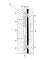
11 p型シリコン基板
12 接続パッド
13 絶縁膜
14 保護膜
15 再配線
16 被覆膜
17 ポストバンプ(柱状の外部接続電極)
18 封止層
19 集積回路部
41 ドライフィルム
Claims (7)
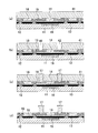
- 複数の配線を備える集積回路部が形成された基板上に、前記集積回路部に電気的に接続された接続パッドを形成する接続パッド形成工程と、
前記接続パッドの一部を露出する接続パッド露出孔を有する絶縁膜及び保護膜を積層して形成する積層工程と、
前記接続パッド露出孔を充填し、且つ、前記保護膜の露出面の一部を覆う副配線を形成する副配線形成工程と、
前記副配線及び前記保護膜を覆う被覆膜を形成する被覆膜形成工程と、
前記被覆膜上にドライフィルムを貼り付けるドライフィルム貼り付け工程と、
前記被覆膜及び前記ドライフィルムを貫通し、前記副配線の一部を露出させる貫通孔を形成する貫通孔形成工程と、
前記貫通孔を充填する外部接続電極を形成する電極形成工程と、
前記ドライフィルムを除去し、前記被覆膜及び前記外部接続電極を覆う封止層を形成する封止層形成工程と、を有し、
前記副配線上に形成された前記被覆膜の膜厚が、前記副配線の膜厚よりも薄いことを特徴とする半導体装置の製造方法。 - 前記被覆膜形成工程は、液状樹脂を塗布して前記被覆膜を形成することを特徴とする請求項1に記載の半導体装置の製造方法。
- 前記被覆膜形成工程は、前記液状樹脂をスピンコート法によって塗布することを特徴とする請求項2に記載の半導体装置の製造方法。
- 前記被覆膜は、ポリイミド系樹脂又はポリベンゾオキサゾール(PBO:Poly Benzo Oxysazole)系樹脂等の有機樹脂からなることを特徴とする請求項3に記載の半導体装置の製造方法。
- 前記被覆膜形成工程は、前記副配線の一部を露出する副配線露出孔を形成する副配線露出孔形成工程を含むことを特徴とする請求項1乃至4のいずれか1に記載の半導体装置の製造方法。
- 前記貫通孔形成工程は、前記副配線露出孔に連通する連通孔を前記ドライフィルムに形成することによって前記貫通孔を形成することを特徴とする請求項5に記載の半導体装置の製造方法。
- 前記被覆膜形成工程は、前記被覆膜を露光することで前記副配線露出孔を形成することを特徴とする請求項5又は6に記載の半導体装置の製造方法。
Priority Applications (2)
| Application Number | Priority Date | Filing Date | Title |
|---|---|---|---|
| JP2008309765A JP5118614B2 (ja) | 2008-12-04 | 2008-12-04 | 半導体装置の製造方法 |
| US12/628,310 US7910478B2 (en) | 2008-12-04 | 2009-12-01 | Method of manufacturing semiconductor devices |
Applications Claiming Priority (1)
| Application Number | Priority Date | Filing Date | Title |
|---|---|---|---|
| JP2008309765A JP5118614B2 (ja) | 2008-12-04 | 2008-12-04 | 半導体装置の製造方法 |
Publications (2)
| Publication Number | Publication Date |
|---|---|
| JP2010135554A JP2010135554A (ja) | 2010-06-17 |
| JP5118614B2 true JP5118614B2 (ja) | 2013-01-16 |
Family
ID=42231561
Family Applications (1)
| Application Number | Title | Priority Date | Filing Date |
|---|---|---|---|
| JP2008309765A Expired - Fee Related JP5118614B2 (ja) | 2008-12-04 | 2008-12-04 | 半導体装置の製造方法 |
Country Status (2)
| Country | Link |
|---|---|
| US (1) | US7910478B2 (ja) |
| JP (1) | JP5118614B2 (ja) |
Families Citing this family (2)
| Publication number | Priority date | Publication date | Assignee | Title |
|---|---|---|---|---|
| JP2014082359A (ja) * | 2012-10-17 | 2014-05-08 | Olympus Corp | 半導体基板、半導体装置、および固体撮像装置、並びに半導体基板の製造方法 |
| US9449908B2 (en) | 2014-07-30 | 2016-09-20 | Taiwan Semiconductor Manufacturing Company, Ltd. | Semiconductor package system and method |
Family Cites Families (7)
| Publication number | Priority date | Publication date | Assignee | Title |
|---|---|---|---|---|
| JP3813367B2 (ja) * | 1998-12-22 | 2006-08-23 | 三洋電機株式会社 | 半導体装置およびその製造方法 |
| JP2003318326A (ja) * | 2002-04-26 | 2003-11-07 | Sony Corp | 半導体装置とその製造方法 |
| JP2004349610A (ja) * | 2003-05-26 | 2004-12-09 | Casio Comput Co Ltd | 半導体装置およびその製造方法 |
| US7541275B2 (en) * | 2004-04-21 | 2009-06-02 | Texas Instruments Incorporated | Method for manufacturing an interconnect |
| JP4949790B2 (ja) | 2006-09-26 | 2012-06-13 | 株式会社テラミクロス | 半導体装置の製造方法 |
| JP2008244383A (ja) | 2007-03-29 | 2008-10-09 | Casio Comput Co Ltd | 半導体装置およびその製造方法 |
| JP4413240B2 (ja) * | 2007-03-05 | 2010-02-10 | Okiセミコンダクタ株式会社 | 半導体装置の製造方法 |
-
2008
- 2008-12-04 JP JP2008309765A patent/JP5118614B2/ja not_active Expired - Fee Related
-
2009
- 2009-12-01 US US12/628,310 patent/US7910478B2/en not_active Expired - Fee Related
Also Published As
| Publication number | Publication date |
|---|---|
| JP2010135554A (ja) | 2010-06-17 |
| US7910478B2 (en) | 2011-03-22 |
| US20100144142A1 (en) | 2010-06-10 |
Similar Documents
| Publication | Publication Date | Title |
|---|---|---|
| TWI582937B (zh) | 封裝結構 | |
| JP4716819B2 (ja) | インターポーザの製造方法 | |
| US8623751B2 (en) | Through-hole electrode substrate and method of manufacturing the same | |
| JP5500464B2 (ja) | マスクを使用せずに導電性ビアに対して裏面位置合わせを行うことによる半導体構成部品の製造方法 | |
| JP2005327984A (ja) | 電子部品及び電子部品実装構造の製造方法 | |
| JP2007103714A (ja) | 半導体装置及びその製造方法 | |
| JP4987928B2 (ja) | 半導体装置の製造方法 | |
| JP2005322858A (ja) | 半導体装置の製造方法 | |
| US8330050B2 (en) | Wiring board having heat intercepting member | |
| TWI690045B (zh) | 構裝結構、其接合方法及用於其的線路板 | |
| JP2010103398A (ja) | 電子部品内蔵基板及びその製造方法 | |
| JP5590985B2 (ja) | 半導体装置及びその製造方法 | |
| TW201640590A (zh) | 電子封裝件及其製法 | |
| KR101139650B1 (ko) | 배선 기판, 그 제조 방법, 및 반도체 장치 | |
| JP2007103716A (ja) | 半導体装置及びその製造方法 | |
| JP2010087229A (ja) | 半導体モジュール、半導体モジュールの製造方法および携帯機器 | |
| TWI543263B (zh) | 半導體裝置及其製造方法 | |
| JP4420965B1 (ja) | 半導体装置内蔵基板の製造方法 | |
| JP5118614B2 (ja) | 半導体装置の製造方法 | |
| JP2008244383A (ja) | 半導体装置およびその製造方法 | |
| JP4764710B2 (ja) | 半導体装置とその製造方法 | |
| JP5466096B2 (ja) | 半導体装置及びその製造方法 | |
| JP2010010249A (ja) | 半導体装置及びその製造方法 | |
| JP2007194472A (ja) | 薄膜キャパシタの製造方法 | |
| JP2007258354A (ja) | 半導体装置の製造方法 |
Legal Events
| Date | Code | Title | Description |
|---|---|---|---|
| A621 | Written request for application examination |
Free format text: JAPANESE INTERMEDIATE CODE: A621 Effective date: 20111129 |
|
| A977 | Report on retrieval |
Free format text: JAPANESE INTERMEDIATE CODE: A971007 Effective date: 20120612 |
|
| A131 | Notification of reasons for refusal |
Free format text: JAPANESE INTERMEDIATE CODE: A131 Effective date: 20120619 |
|
| A521 | Request for written amendment filed |
Free format text: JAPANESE INTERMEDIATE CODE: A523 Effective date: 20120820 |
|
| TRDD | Decision of grant or rejection written | ||
| A01 | Written decision to grant a patent or to grant a registration (utility model) |
Free format text: JAPANESE INTERMEDIATE CODE: A01 Effective date: 20120925 |
|
| A01 | Written decision to grant a patent or to grant a registration (utility model) |
Free format text: JAPANESE INTERMEDIATE CODE: A01 |
|
| A61 | First payment of annual fees (during grant procedure) |
Free format text: JAPANESE INTERMEDIATE CODE: A61 Effective date: 20121019 |
|
| R150 | Certificate of patent or registration of utility model |
Free format text: JAPANESE INTERMEDIATE CODE: R150 Ref document number: 5118614 Country of ref document: JP Free format text: JAPANESE INTERMEDIATE CODE: R150 |
|
| FPAY | Renewal fee payment (event date is renewal date of database) |
Free format text: PAYMENT UNTIL: 20151026 Year of fee payment: 3 |
|
| S531 | Written request for registration of change of domicile |
Free format text: JAPANESE INTERMEDIATE CODE: R313531 |
|
| R350 | Written notification of registration of transfer |
Free format text: JAPANESE INTERMEDIATE CODE: R350 |
|
| LAPS | Cancellation because of no payment of annual fees |