JP5100944B2 - Light emitting semiconductor device with luminescence conversion element - Google Patents
Light emitting semiconductor device with luminescence conversion element Download PDFInfo
- Publication number
- JP5100944B2 JP5100944B2 JP2001579375A JP2001579375A JP5100944B2 JP 5100944 B2 JP5100944 B2 JP 5100944B2 JP 2001579375 A JP2001579375 A JP 2001579375A JP 2001579375 A JP2001579375 A JP 2001579375A JP 5100944 B2 JP5100944 B2 JP 5100944B2
- Authority
- JP
- Japan
- Prior art keywords
- emitting semiconductor
- semiconductor device
- light
- luminescence conversion
- conversion element
- Prior art date
- Legal status (The legal status is an assumption and is not a legal conclusion. Google has not performed a legal analysis and makes no representation as to the accuracy of the status listed.)
- Expired - Fee Related
Links
Images

Classifications
-
- H—ELECTRICITY
- H01—ELECTRIC ELEMENTS
- H01L—SEMICONDUCTOR DEVICES NOT COVERED BY CLASS H10
- H01L33/00—Semiconductor devices with at least one potential-jump barrier or surface barrier specially adapted for light emission; Processes or apparatus specially adapted for the manufacture or treatment thereof or of parts thereof; Details thereof
- H01L33/48—Semiconductor devices with at least one potential-jump barrier or surface barrier specially adapted for light emission; Processes or apparatus specially adapted for the manufacture or treatment thereof or of parts thereof; Details thereof characterised by the semiconductor body packages
- H01L33/483—Containers
- H01L33/486—Containers adapted for surface mounting
-
- H—ELECTRICITY
- H01—ELECTRIC ELEMENTS
- H01L—SEMICONDUCTOR DEVICES NOT COVERED BY CLASS H10
- H01L33/00—Semiconductor devices with at least one potential-jump barrier or surface barrier specially adapted for light emission; Processes or apparatus specially adapted for the manufacture or treatment thereof or of parts thereof; Details thereof
- H01L33/48—Semiconductor devices with at least one potential-jump barrier or surface barrier specially adapted for light emission; Processes or apparatus specially adapted for the manufacture or treatment thereof or of parts thereof; Details thereof characterised by the semiconductor body packages
- H01L33/50—Wavelength conversion elements
- H01L33/505—Wavelength conversion elements characterised by the shape, e.g. plate or foil
-
- H—ELECTRICITY
- H01—ELECTRIC ELEMENTS
- H01L—SEMICONDUCTOR DEVICES NOT COVERED BY CLASS H10
- H01L2224/00—Indexing scheme for arrangements for connecting or disconnecting semiconductor or solid-state bodies and methods related thereto as covered by H01L24/00
- H01L2224/01—Means for bonding being attached to, or being formed on, the surface to be connected, e.g. chip-to-package, die-attach, "first-level" interconnects; Manufacturing methods related thereto
- H01L2224/42—Wire connectors; Manufacturing methods related thereto
- H01L2224/47—Structure, shape, material or disposition of the wire connectors after the connecting process
- H01L2224/48—Structure, shape, material or disposition of the wire connectors after the connecting process of an individual wire connector
- H01L2224/4805—Shape
- H01L2224/4809—Loop shape
- H01L2224/48091—Arched
-
- H—ELECTRICITY
- H01—ELECTRIC ELEMENTS
- H01L—SEMICONDUCTOR DEVICES NOT COVERED BY CLASS H10
- H01L2224/00—Indexing scheme for arrangements for connecting or disconnecting semiconductor or solid-state bodies and methods related thereto as covered by H01L24/00
- H01L2224/01—Means for bonding being attached to, or being formed on, the surface to be connected, e.g. chip-to-package, die-attach, "first-level" interconnects; Manufacturing methods related thereto
- H01L2224/42—Wire connectors; Manufacturing methods related thereto
- H01L2224/47—Structure, shape, material or disposition of the wire connectors after the connecting process
- H01L2224/48—Structure, shape, material or disposition of the wire connectors after the connecting process of an individual wire connector
- H01L2224/481—Disposition
- H01L2224/48151—Connecting between a semiconductor or solid-state body and an item not being a semiconductor or solid-state body, e.g. chip-to-substrate, chip-to-passive
- H01L2224/48221—Connecting between a semiconductor or solid-state body and an item not being a semiconductor or solid-state body, e.g. chip-to-substrate, chip-to-passive the body and the item being stacked
- H01L2224/48245—Connecting between a semiconductor or solid-state body and an item not being a semiconductor or solid-state body, e.g. chip-to-substrate, chip-to-passive the body and the item being stacked the item being metallic
- H01L2224/48247—Connecting between a semiconductor or solid-state body and an item not being a semiconductor or solid-state body, e.g. chip-to-substrate, chip-to-passive the body and the item being stacked the item being metallic connecting the wire to a bond pad of the item
-
- H—ELECTRICITY
- H01—ELECTRIC ELEMENTS
- H01L—SEMICONDUCTOR DEVICES NOT COVERED BY CLASS H10
- H01L2224/00—Indexing scheme for arrangements for connecting or disconnecting semiconductor or solid-state bodies and methods related thereto as covered by H01L24/00
- H01L2224/01—Means for bonding being attached to, or being formed on, the surface to be connected, e.g. chip-to-package, die-attach, "first-level" interconnects; Manufacturing methods related thereto
- H01L2224/42—Wire connectors; Manufacturing methods related thereto
- H01L2224/47—Structure, shape, material or disposition of the wire connectors after the connecting process
- H01L2224/48—Structure, shape, material or disposition of the wire connectors after the connecting process of an individual wire connector
- H01L2224/484—Connecting portions
- H01L2224/4847—Connecting portions the connecting portion on the bonding area of the semiconductor or solid-state body being a wedge bond
- H01L2224/48471—Connecting portions the connecting portion on the bonding area of the semiconductor or solid-state body being a wedge bond the other connecting portion not on the bonding area being a ball bond, i.e. wedge-to-ball, reverse stitch
-
- H—ELECTRICITY
- H01—ELECTRIC ELEMENTS
- H01L—SEMICONDUCTOR DEVICES NOT COVERED BY CLASS H10
- H01L2224/00—Indexing scheme for arrangements for connecting or disconnecting semiconductor or solid-state bodies and methods related thereto as covered by H01L24/00
- H01L2224/80—Methods for connecting semiconductor or other solid state bodies using means for bonding being attached to, or being formed on, the surface to be connected
- H01L2224/85—Methods for connecting semiconductor or other solid state bodies using means for bonding being attached to, or being formed on, the surface to be connected using a wire connector
- H01L2224/85909—Post-treatment of the connector or wire bonding area
- H01L2224/8592—Applying permanent coating, e.g. protective coating
-
- H—ELECTRICITY
- H01—ELECTRIC ELEMENTS
- H01L—SEMICONDUCTOR DEVICES NOT COVERED BY CLASS H10
- H01L2924/00—Indexing scheme for arrangements or methods for connecting or disconnecting semiconductor or solid-state bodies as covered by H01L24/00
- H01L2924/0001—Technical content checked by a classifier
- H01L2924/00014—Technical content checked by a classifier the subject-matter covered by the group, the symbol of which is combined with the symbol of this group, being disclosed without further technical details
-
- H—ELECTRICITY
- H01—ELECTRIC ELEMENTS
- H01L—SEMICONDUCTOR DEVICES NOT COVERED BY CLASS H10
- H01L2924/00—Indexing scheme for arrangements or methods for connecting or disconnecting semiconductor or solid-state bodies as covered by H01L24/00
- H01L2924/10—Details of semiconductor or other solid state devices to be connected
- H01L2924/11—Device type
- H01L2924/12—Passive devices, e.g. 2 terminal devices
- H01L2924/1204—Optical Diode
- H01L2924/12041—LED
-
- H—ELECTRICITY
- H01—ELECTRIC ELEMENTS
- H01L—SEMICONDUCTOR DEVICES NOT COVERED BY CLASS H10
- H01L2924/00—Indexing scheme for arrangements or methods for connecting or disconnecting semiconductor or solid-state bodies as covered by H01L24/00
- H01L2924/15—Details of package parts other than the semiconductor or other solid state devices to be connected
- H01L2924/181—Encapsulation
-
- H—ELECTRICITY
- H01—ELECTRIC ELEMENTS
- H01L—SEMICONDUCTOR DEVICES NOT COVERED BY CLASS H10
- H01L2933/00—Details relating to devices covered by the group H01L33/00 but not provided for in its subgroups
- H01L2933/0008—Processes
- H01L2933/0033—Processes relating to semiconductor body packages
- H01L2933/0041—Processes relating to semiconductor body packages relating to wavelength conversion elements
-
- H—ELECTRICITY
- H01—ELECTRIC ELEMENTS
- H01L—SEMICONDUCTOR DEVICES NOT COVERED BY CLASS H10
- H01L33/00—Semiconductor devices with at least one potential-jump barrier or surface barrier specially adapted for light emission; Processes or apparatus specially adapted for the manufacture or treatment thereof or of parts thereof; Details thereof
- H01L33/48—Semiconductor devices with at least one potential-jump barrier or surface barrier specially adapted for light emission; Processes or apparatus specially adapted for the manufacture or treatment thereof or of parts thereof; Details thereof characterised by the semiconductor body packages
- H01L33/58—Optical field-shaping elements
- H01L33/60—Reflective elements
-
- H—ELECTRICITY
- H01—ELECTRIC ELEMENTS
- H01L—SEMICONDUCTOR DEVICES NOT COVERED BY CLASS H10
- H01L33/00—Semiconductor devices with at least one potential-jump barrier or surface barrier specially adapted for light emission; Processes or apparatus specially adapted for the manufacture or treatment thereof or of parts thereof; Details thereof
- H01L33/48—Semiconductor devices with at least one potential-jump barrier or surface barrier specially adapted for light emission; Processes or apparatus specially adapted for the manufacture or treatment thereof or of parts thereof; Details thereof characterised by the semiconductor body packages
- H01L33/62—Arrangements for conducting electric current to or from the semiconductor body, e.g. lead-frames, wire-bonds or solder balls
Description
【0001】
本発明は、独立請求項の上位概念に記載の光放出半導体素子並びに該半導体素子の製造方法に関する。
【0002】
光放出半導体素子は例えばWO97/50132号から公知である。この種の素子は、作動中光を出す(1次光)半導体基体と、この光の一部を別の波長領域に変換する(ルミネセンス光ないし蛍光)発光変換、すなわちルミネセンス変換エレメントとを含んでいる。この種の半導体素子から放出される光の全体としての色の印象は、1次光と蛍光との加算的な色混合によって生じるものである。
【0003】
ルミネセンス変換エレメントとして、合成樹脂に懸濁混入されている蛍光体が使用されることが多い。WO97/50132号に示されているように、光放出半導体素子の構造形態の特徴は、素子基体の凹所に半導体基体を配置しかつこの凹所に蛍光体懸濁液を充填することである。
【0004】
この配置構成は、1次光のソース−半導体基体−および蛍光のソース−蛍光体懸濁液−が一般に異なった形状およびサイズをしているので、放射方向に応じて異なった色成分への分解が行われかつ空間的に不均質な色印象が生じるという欠点を有してる。
【0005】
別の欠点は次の点にある:色印象は懸濁液中の光路長に依存しているので、半導体基体上の懸濁液層の厚さが製造に規定されて変動することで種々の色印象が生じることになる。更に基本的に、懸濁液中に蛍光体の非常に均質な分配が必要である。
【0006】
本発明の課題は、冒頭に述べた形式の光放出半導体素子を、均質な混色光を放射するように改良することである。更に本発明の課題は、この種の素子に対する製造方法を提供することである。
【0007】
この課題は、独立請求項に記載の半導体素子並びに方法によって解決される。本発明の有利な実施形態は従属請求項の対象である。
【0008】
本発明によれば、半導体素子の基体を次のように実現するようになっている:半導体基体を収容するために形成されている凹所において半導体基体の直接的な周囲において、別個の、小鉢形式の領域が成形されており、該領域がルミネセンス変換エレメントを含んでいる。半導体基体にルミネセンス変換エレメントを、凹所全体を充填する大容量で被覆することに比べて、この配置構成は、蛍光が1次光とほぼ同一のボリュームから放射され、これにより特別均質な色印象が生じるという利点を有している。
【0009】
特別有利な実施形態では、ルミネセンス変換エレメントを収容するための別個の領域は凹所内のくぼみによって成形されている。別の特別有利な実施形態では、別個の領域を凹所の底面上のリング形状の囲いよって成形している。両方の実施形態とも非常に有利なことに、基体として標準形状のケーシングを使用することができる。
【0010】
有利には、くぼみないしリング形状の囲いの側面は、該側面が生成された放射線に対するリフレクタとして用いられかつこのようにして発光効率が高められるように成形されている。
【0011】
本発明の有利な発展形態によれば、基体にリードフレームが次のように埋め込まれている:リードフレームの部分が上述した一方の実施形態ではくぼみの底面を形成しているかまたはリードフレーム上に上述した他方の実施形態のリング形状の囲いが成形されている。半導体基体はこの実施形態ではリードフレームに配置されており、その際電気的なコンタクト形成は直接(チップ・ボンディング)またはワイヤ接続を用いて(ワイヤ・ボンディング)行われるようにすることができる。この所謂リードフレーム技術は光放出半導体素子では多岐にわたって適用されかつ本発明にも有利に使用することができる。
【0012】
半導体基体およびルミネセンス変換エレメントを保護するために、凹所に透光性の充填材、例えば注型成形材を充填することができる。有利にはこの充填材は反応性樹脂、例えばアクリル樹脂、エポキシ樹脂、シリコーン樹脂またはこれら樹脂の混合物を含んでいる。充填材の適当な成形によって、本発明の素子の放射特性を一段と改善するまたは所望通り修正するレンズ作用または散乱作用が得られるようにすることができる。また、自動的な実装装置に対しては、充填材を用いて素子に平坦な表面を形成すると有利である。というのは、このような素子は自動実装装置によって比較的容易に受け取られかつ位置決めすることができるからである(ピック・アンド・プレイス法)。
【0013】
特別簡単な実現能力に基づいて有利である実施形態では、ルミネセンス変換エレメントは、マトリックスに埋め込まれている1つまたは複数の蛍光体から成っている。マトリックスとして、混合能力、柔軟性および取り扱いに関して特に、アクリル樹脂、エポキシ樹脂およびシリコーン樹脂並びにその混合物が適している。
【0014】
蛍光体として一方において、ペリレン色素または4f−有機金属化合物のような有機化合物を混入させることができる。すなわち、BASF社のLumogenF083, LumogenF240およびLumogenF300のような蛍光体は簡単な手法で透明なエポキシ樹脂に添加される。
【0015】
全体として白い色印象は無機蛍光体の使用によって実現することができる。このために殊に適しているのは、希土類でドープされているガーネット並びに希土類でドープされているアルカリ土類金属硫化物である。
【0016】
この場合効率のよい蛍光体は、化学式A3B5O12:Mを充足する化合物である(これらが通例の製造および作動条件下で不安定でない場合には)。ここでAはグループY,Lu,Sc,La.Gd,TbおよびSmの少なくとも1つの元素であり、BはグループAl,GaおよびInの少なくとも1つの元素でありかつMはグループCeおよびPrの少なくとも1つの元素、有利にはCeである。この場合蛍光体として特別有利には、YAG:Ce(Y3Al5012:Ce3+)、TbYAG:Ce((YxTb1−x)3Al5O12:Ce3+,0≦x≦1)、GdYAG:Ce((GdxY1−x)3Al5O12:Ce3+,0<x<1)、GdTbYAG:Ce((GdxTbyY1−x−y)3Al5O12:Ce3,0<x<1,0<y<1)並びにこれらに基づいている混合物である。その際Alは少なくとも部分的にGaまたはInによって置換することができる。更に有利なのは化合物SrS:Ce3+,Na,SrS:Ce3+,Cl,Srs:CeCl3,CaS:Ce3+,SrSe:Ce3+およびY3Ga5O12:Ce3+である。
【0017】
種々様々な形式の混合色の光を生成するために、例えばCaGa2S4:Ce3+またはSrGa2S4:Ce3+のような、希土類が添加されているチオ没食子酸塩が適している。このために同様に、例えばYAlO3:Ce3+およびYAl1−xGaxO3:Ce3+,0≦x≦1のような、希土類が添加されているアルミン酸塩および例えばY2SiO5:Ce3+のような、希土類が添加されているオルトケイ酸塩M′2SiO5:Ce3+(M′:Sc,Y,La)である。すべてのイットリウム化合物においてイットリウムは原理的にスカンジウムまたはランタンによって置換することができる。その際蛍光体のそれぞれの組成はまず第1に、所望の全体の色の印象並びに1次光の中心波長から決められる。
【0018】
別の特別有利な実施形態において、ルミネセンス変換エレメントに対するマトリックスとしておよび凹所における充填材として種々の材料が使用される。その際ルミネセンス変換エレメントに対して有利には、蛍光体との混合性および放射耐性に関して最適である材料が使用され、一方充填材に対して、透過性および機械的な耐性に基づいて特別適している材料が選択される。
【0019】
充填材およびルミネセンス変換エレメントのマトリックスの選択の際のこのような付加的な可能な変形態様によって非常に有利にも、ルミネセンス変換エレメントを有する光放出半導体素子の実現の際の別の縁条件を充足させることができる。
【0020】
特別有利には、本発明の素子において、460nmを下回る中心波長を有する光を放射する半導体基体を使用することができる。この種の半導体基体の使用は上で述べた従来技術の素子では有意味ではない。というのは、この波長領域における光は充填材を傷つける可能性があり、その場合充填材が非常に迅速に老化するからである。この欠点は本発明の素子では大幅に取り除かれている。というのは、1次光の一部が半導体基体の非常に近傍で変換され、その結果充填材における波長の短い放射線の割合が低減されかつ全体として素子の寿命が延長されるからである。
【0021】
有利には、ルミネセンス変換エレメントに対するマトリックスとしてシリコーン樹脂が使用される。これは緑、青および紫のスペクトル領域における特別高い放射耐性によって傑出している。シリコーン樹脂の使用は、430nm以下の波長を有する放射線を放出する半導体基体との関連において特別有利である。このスペクトル領域における放射線では別の樹脂の場合放射損傷が生じる可能性があり、素子の寿命が著しく低減されることになる。シリコーン樹脂マトリックスを有するルミネセンス変換エレメントは本発明においては、ルミネセンス変換エレメントを被覆する、エポキシ樹脂をベースとしている充填材と組み合わせることができる。この場合エポキシ樹脂は高い透明度および機械的な安定性によって傑出している。
【0022】
特別有利にも、本発明の部品によって、上に挙げたWO97/50132号に記載されているような白色発光ダイオードが実現される。蛍光体および半導体基体はこの場合、1次光の色および蛍光が相互に補色であるように相互調整されている。加法色混合によって白色光の印象が引き起こされる。WO97/50132号およびWO98/12757号の内容は本明細書の内容に組み入れられる。
【0023】
本発明の素子の多数個を比較的大きな照明ユニットに組み合わせることができる。場合によっては素子がマトリックス形状に配置されているこの種の照明ユニットは、高い輝度および全体としての均質な色の印象によって傑出している。
【0024】
特別有利にも本発明の素子は結像レンズ系における光源として適している。1次光および蛍光は空間的に密接しておりかつ大体同じ大きさのボリュームから放射されるので、この種のレンズ系が引き起こす色の歪みは従来技術による光源の場合よりも著しく小さい。それ故に更に有利にも、本発明の素子の放射特性を1つまたは複数のレンズを用いて全体の色の印象を変えることなく修正することができる。
【0025】
ルミネセンス変換エレメントを備えた光放出半導体素子の本発明の製造方法の出発点は凹所をもっている基体であって、基体にはリードフレームが埋め込まれていて、その結果リードフレームの部分領域が凹所の底面を形成している。まず、リードフレームが成形材によって射出され、その際チップ接続領域は空所になっている。この空所がルミネセンス変換エレメントを収容するための別個の領域を形成する。その後、半導体基体はリードフレームのこのチップ接続領域にマウントされかつ作動のために必要な電気的な接続体が半導体基体とリードフレームとの間に形成される。次のステップにおいて、この空いている領域にルミネセンス変換エレメントが充填され、その際半導体基体はルミネセンス変換エレメント内に完全に埋め込まれる。
【0026】
別の本発明の製造方法において、同じく出発原料として凹所を備えた基体が使用され、そこにはリードフレームが、該リードフレームの一部が凹所の底面を形成するように埋め込まれている。リードフレームにはチップ接続領域の周りに成形材によってリング形状の囲いが成形される。この囲いの内部領域は、ルミネセンス変換エレメントを収容するための別個の領域を形成している。この囲いの内で、リードフレームのチップ接続領域に半導体基体が被されかつ作動のために必要な、半導体基体とリードフレームとの間の電気的な接続が形成される。次のステップにおいて、囲いはルミネセンス変換エレメントで満たされ、その際半導体基体は完全にルミネセンス変換エレメント内に埋め込まれる。
【0027】
2つの方法とも、出発材料として、標準形状のケーシングをもった標準ケーシングないし基体を使用することができるという利点を有している。ルミネセンス変換エレメントを収容するための別個の領域の成形は本発明の素子の製造プロセスに容易に組み入れることができる。
【0028】
本発明の有利な発展形態では、凹所は透光性の充填材、例えば相応の注入鋳込み材によって充填される。半導体基体の被覆は2つのステップにおいて行われるので、有利にも半導体基体の、被覆からの剥離および被覆内の亀裂発生が低減されかつこれにより素子の耐湿性および寿命が高められる。
【0029】
別の特徴および利点は図1ないし4と関連した4つの実施例の以下の説明から明らかである。
【0030】
その際:
図1は、ルミネセンス変換エレメントを備えた本発明の光放出半導体素子の第1実施例の断面略図であり、
図2は、ルミネセンス変換エレメントを備えた本発明の光放出半導体素子の第2実施例の断面略図であり、
図3は、本発明の製造方法の第1実施例の略図であり、
図4は、本発明の製造方法の第2実施例の略図である。
【0031】
種々の図には、同じないし同じ作用をする部分には同じ参照番号が付されている。
【0032】
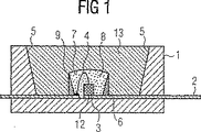
図1に図示の本発明の半導体素子は基体1として標準ケーシングを有している。これは例えば、熱可塑性樹脂から成っている表面実装可能なLEDケーシングであってよい。側壁5は軽く勾配をつけられておりかつ生成された放射線に対するリフレクタとして作用する。基体1にリードフレーム2が収容されている。リードフレーム2のチップ接続領域12に半導体基体3がボンディングされておりかつワイヤ接続部4を介してリードフレーム2のワイヤ接続領域11に電気的に接続されている。半導体基体の形状に応じて、半導体基体3のコンタクト形成は複数のワイヤ接続部を介して行うこともできる。
【0033】
半導体基体3の周囲に比較的小さなリフレクタリング6が成形されている。有利にはこのリフレクタリングに対する材料として、同様に熱可塑性樹脂を使用することができる。リフレクタリング6にはルミネセンス変換エレメントが充填されている。これは例えばシリコーンのようなマトリックス中の蛍光体の懸濁液から成っている。シリコーンはそのエージング安定性に基づいて、短い波長(青、UV)を放出する半導体基体3が使用される場合殊に適している。
【0034】
リフレクタリング6の構造高さとして、0.3mmと0.7mmとの間の寸法が特別有利であることが分かっている。このサイズのリフレクタにより一方において半導体基体3をルミネセンス変換エレメント7で覆うことが保証され、しかも他方においてルミネセンス変換エレメント7のボリュームを拡大する必要はない。
【0035】
この場合、シャープなエッジ9を持ったリフレクタリング6を成形すると特別有利である。これにより、リフレクタリング6が充填されている場合蛍光体混濁液がその表面張力に基づいてリフレクタリング6上に円頂が形成されるようになり、これにより半導体基体3の、ルミネセンス変換エレメント7への完全な埋め込みがほぼ保証される。
【0036】
凹所の依然として残っている部分には、例えばエポキシ樹脂のような透明な注型成形材13で充たされている。
【0037】
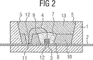
図2に図示の本発明の半導体素子は図1に図示の素子とは次の点で相異している:ルミネセンス変換エレメント7を収容するための半導体基体3の周りの領域はリードフレーム2のチップ接続領域12上のくぼみによって成形されている。このためにリードフレーム2は薄い成形材層10(高さは有利には同様に0.3mmないし0.7mm)によってカバーされており、その際くぼみはチップ接続領域12上の成形材層10の切り欠きによって形成されている。上に説明した実施例の場合のように切り欠きが、半導体基体3上にルミネセンス変換エレメント7の円頂を形成するためのシャープなエッジ9を持っているように成形されていれば有利である。成形材が欠けている、半導体基体3周辺の領域にはルミネセンス変換エレメント7が充填されている。
【0038】
図示の実施例では更に、ワイヤ接続領域11の成形材層10が切り欠かれている。この切り欠きは、該切り欠きの側面がケーシング側面5より下がっている形状になっている。これにより、製造時にワイヤ接続領域11上の切り欠きに侵入する可能性がある蛍光体懸濁液の部分がケーシング壁5を上るように流れることが妨げられる。このような上に向かう流れはとりわけケーシング壁5に凹凸があると効果を発揮し、不都合である。というのはこれにより蛍光の放射領域は拡大されるからである。
【0039】
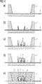
図3には本発明の製造方法の実施例が略示されている。
【0040】
第1ステップにおいて、図3a)に示されているように、例えば、射出成形法においてリードフレーム2にケーシング成形材を射出することによって、凹所を有しかつリードフレーム2が集積されている基体1が製造される。
【0041】
次のステップにおいて、リードフレーム2に成形材、例えばPPAが射出され、その結果リードフレーム2は同じにとどまる厚さを有する成形材層10によって被覆される。その際リードフレーム2のチップ接続領域12およびワイヤ接続領域11は露出されている(図3b)。これとは択一的に、図3bに示されているケーシング形状を勿論唯一の工程で形成することもできる。
【0042】
これに続いて半導体基体3がチップ接続領域12にボンディングされかつ半導体基体3とリードフレーム2との間のワイヤ接続部4が形成される(図3c)。ボンディングの完了後、半導体基体3の周りの空所にルミネセンス変換エレメント7、例えば合成樹脂中の蛍光体の懸濁液が充填される(図3d)。
【0043】
最後に図3eに示されているように、例えばエポキシ樹脂のような透光性の材料を用いた素子の注型成形(13)を行うことができる。素子に対する要求に応じて、注型成形の表面を平面的に、レンズ形状に、突起を有しているようにまたは散乱ディスクとして実現することができる。
【0044】
図4に示されている本発明の方法の実施例では、第1のステップでは同様に空所を有しかつリードフレーム2が埋め込まれている基体1が製造される(図4a)。
【0045】
その後、チップ接続領域12を取り囲むリフレクタリング6が射出成形される(図4b)。この場合も、基体1およびリフレクタリング6の製造は唯一の製造ステップで行うことができる。半導体基体3がこれに続いてリードフレーム2のチップ接続領域12にマウントされかつコンタクト形成される(図4c)。次のステップにおいてリフレクタリング6に、蛍光体懸濁液の形のルミネセンス変換エレメント7が充填され、その際リフレクタリング6のシャープなエッジの縁形成9および蛍光体懸濁液の表面張力に基づいて、図4dに示されているように、半導体基体3上に円頂が形成される。これにより、ルミネセンス変換エレメント7のボリュームを不必要に拡大することなく、半導体基体3の完全な被覆が保証される。
【0046】
先に示した実施例と同様に、その後で素子を注型成形することができる(図4e)。
【0047】
これまで行った実施例に基づく本発明の説明は勿論、本発明をそれに制限するものではない。
【図面の簡単な説明】
【図1】 ルミネセンス変換エレメントを備えた本発明の光放出半導体素子の第1実施例の断面略図である。
【図2】 ルミネセンス変換エレメントを備えた本発明の光放出半導体素子の第2実施例の断面略図である。
【図3】 本発明の製造方法の第1実施例の略図である。
【図4】 本発明の製造方法の第2実施例の略図である。[0001]
The present invention relates to a process for producing the semiconductor device in the light-emitting semiconductor device arrangement according to the preamble of the independent claims.
[0002]
Light emitting semiconductor elements are known, for example, from WO 97/50132. This type of element comprises a semiconductor substrate that emits light during operation (primary light) and a luminescence conversion, ie a luminescence conversion element, that converts part of this light into another wavelength region (luminescence light or fluorescence). Contains. The overall color impression of light emitted from this type of semiconductor device is caused by additive color mixing of primary light and fluorescence.
[0003]
As the luminescence conversion element, a phosphor suspended in a synthetic resin is often used. As shown in WO97 / 50132, the feature of the structure of the light emitting semiconductor device is that the semiconductor substrate is disposed in the recess of the device substrate and the recess is filled with the phosphor suspension. .
[0004]
In this arrangement, the primary light source—the semiconductor substrate—and the fluorescent source—the phosphor suspension—has generally different shapes and sizes, so that they are separated into different color components depending on the direction of emission. And a spatially inhomogeneous color impression is produced.
[0005]
Another drawback lies in the following: the color impression depends on the optical path length in the suspension, so that the thickness of the suspension layer on the semiconductor substrate varies as defined by the manufacturing A color impression will occur. Furthermore, basically a very homogeneous distribution of the phosphor in the suspension is necessary.
[0006]
An object of the present invention is to improve a light-emitting semiconductor device of the type described at the beginning so as to emit homogeneous color mixing light. It is a further object of the present invention to provide a manufacturing method for this type of device.
[0007]
This problem is solved by a method in a semiconductor device arrangement according to the independent claim. Advantageous embodiments of the invention are the subject of the dependent claims.
[0008]
According to the present invention, the substrate of the semiconductor element is realized as follows: in a recess formed to receive the semiconductor substrate, a separate, small bowl directly around the semiconductor substrate. A region of the form is shaped and contains the luminescence conversion element. Compared to coating a semiconductor substrate with a luminescence conversion element with a large volume that fills the entire recess, this arrangement allows the fluorescence to be emitted from approximately the same volume as the primary light, thereby providing a particularly homogeneous color. It has the advantage of creating an impression.
[0009]
In a particularly advantageous embodiment, the separate area for accommodating the luminescence conversion element is shaped by a recess in the recess. In another particularly advantageous embodiment, the separate areas are shaped by a ring-shaped enclosure on the bottom surface of the recess. In both embodiments it is very advantageous to use a standard shaped casing as the substrate.
[0010]
Advantageously, the side surface of the indentation or ring-shaped enclosure is shaped so that it can be used as a reflector for the radiation generated and in this way the luminous efficiency is increased.
[0011]
According to an advantageous development of the invention, the lead frame is embedded in the substrate as follows: the lead frame part forms the bottom of the indentation in one embodiment described above or on the lead frame. The ring-shaped enclosure of the other embodiment described above is formed. In this embodiment, the semiconductor substrate is arranged on a lead frame, in which case the electrical contact can be made directly (chip bonding) or using wire connection (wire bonding). This so-called lead frame technology is widely applied to light emitting semiconductor devices and can be used advantageously in the present invention.
[0012]
In order to protect the semiconductor substrate and the luminescence conversion element, the recess can be filled with a translucent filler, such as a cast molding material. The filler preferably comprises a reactive resin such as an acrylic resin, an epoxy resin, a silicone resin or a mixture of these resins. Appropriate shaping of the filler can result in a lens or scattering effect that further improves or modifies the radiation characteristics of the element of the invention as desired. In addition, for an automatic mounting apparatus, it is advantageous to form a flat surface on the element using a filler. This is because such elements can be received and positioned relatively easily by an automatic mounting device (pick and place method).
[0013]
In an advantageous embodiment on the basis of a particularly simple realization capability, the luminescence conversion element consists of one or more phosphors embedded in a matrix. As the matrix, acrylic resins, epoxy resins and silicone resins and mixtures thereof are particularly suitable with regard to mixing capacity, flexibility and handling.
[0014]
On the one hand as phosphors, organic compounds such as perylene dyes or 4f-organometallic compounds can be incorporated. That is, phosphors such as BASF Lumogen F083, Lumogen F240, and Lumogen F300 are added to a transparent epoxy resin by a simple method.
[0015]
The overall white color impression can be realized by the use of inorganic phosphors. Particularly suitable for this purpose are garnets doped with rare earths and alkaline earth metal sulfides doped with rare earths.
[0016]
Efficient phosphors in this case are compounds satisfying the chemical formula A 3 B 5 O 12 : M (if they are not unstable under customary manufacturing and operating conditions). Here, A is a group Y, Lu, Sc, La. At least one element of Gd, Tb and Sm, B is at least one element of the groups Al, Ga and In and M is at least one element of the groups Ce and Pr, preferably Ce. In this case, YAG: Ce (Y 3 Al 5 0 12 : Ce 3+ ), TbYAG: Ce ((Y x Tb 1-x ) 3 Al 5 O 12 : Ce 3+ , 0 ≦ x ≦ 1), GdYAG: Ce (( Gd x Y 1-x) 3 Al 5 O 12: Ce 3+, 0 <x <1), GdTbYAG: Ce ((Gd x Tb y Y 1-x-y) 3 Al 5 O 12 : Ce 3 , 0 <x <1, 0 <y <1) and mixtures based on these. In this case, Al can be at least partially replaced by Ga or In. Further preferred are the compounds SrS: Ce 3+ , Na, SrS: Ce 3+ , Cl, Srs: CeCl 3 , CaS: Ce 3+ , SrSe: Ce 3+ and Y 3 Ga 5 O 12 : Ce 3+ .
[0017]
To generate light of various types of mixed colors, thiogallates to which rare earths are added, such as CaGa 2 S 4 : Ce 3+ or SrGa 2 S 4 : Ce 3+ are suitable. For this, likewise, for example YAlO 3 : Ce 3+ and YAl 1-x Ga x O 3 : Ce 3+ , aluminates to which rare earths have been added, such as 0 ≦ x ≦ 1, and for example Y 2 SiO 5 : such as Ce 3+, orthosilicic rare earth is added salt M '2 SiO 5: Ce 3+ (M': Sc, Y, La) is. In all yttrium compounds, yttrium can in principle be replaced by scandium or lanthanum. In this case, the composition of each of the phosphors is first determined from the desired overall color impression and the central wavelength of the primary light.
[0018]
In another particularly advantageous embodiment, various materials are used as a matrix for the luminescence conversion element and as a filler in the recess. In this case, a material that is optimal for mixing with the phosphor and radiation resistance is preferably used for the luminescence conversion element, while it is particularly suitable for the filler on the basis of transparency and mechanical resistance. Material is selected.
[0019]
Such additional possible variations in the selection of the filler and the matrix of the luminescence conversion element very advantageously make it possible to achieve further edge conditions in the realization of a light-emitting semiconductor device with a luminescence conversion element. Can be satisfied.
[0020]
It is particularly advantageous to use a semiconductor substrate that emits light having a central wavelength below 460 nm in the device according to the invention. The use of this type of semiconductor substrate is not meaningful in the prior art devices described above. This is because light in this wavelength region can damage the filler, in which case the filler ages very quickly. This disadvantage is largely eliminated in the device of the present invention. This is because a portion of the primary light is converted very close to the semiconductor substrate, resulting in a reduction in the proportion of short-wavelength radiation in the filler and overall increase in device lifetime.
[0021]
Advantageously, a silicone resin is used as a matrix for the luminescence conversion element. This is distinguished by an exceptionally high radiation resistance in the green, blue and purple spectral regions. The use of silicone resins is particularly advantageous in connection with semiconductor substrates that emit radiation having a wavelength of 430 nm or less. Radiation in this spectral region can cause radiative damage in the case of other resins, resulting in a significant reduction in device lifetime. A luminescence conversion element having a silicone resin matrix can be combined in the present invention with an epoxy resin-based filler covering the luminescence conversion element. In this case, the epoxy resin is outstanding due to its high transparency and mechanical stability.
[0022]
Particularly advantageously, the components according to the invention realize a white light-emitting diode as described in WO 97/50132 cited above. In this case, the phosphor and the semiconductor substrate are mutually adjusted so that the color of primary light and the fluorescence are complementary colors. The additive color mixture causes the impression of white light. The contents of WO 97/50132 and WO 98/12757 are incorporated herein by reference.
[0023]
Multiple elements of the present invention can be combined in a relatively large lighting unit. This type of lighting unit, in which the elements are sometimes arranged in a matrix, is distinguished by a high brightness and an overall homogeneous color impression.
[0024]
The element according to the invention is particularly suitable as a light source in an imaging lens system. Since primary light and fluorescence are spatially in close proximity and are emitted from roughly the same volume, the color distortion caused by this type of lens system is significantly less than with prior art light sources. It is therefore further advantageous that the radiation characteristics of the element of the invention can be modified using one or more lenses without changing the overall color impression.
[0025]
The starting point of the manufacturing method of the present invention for a light-emitting semiconductor device having a luminescence conversion element is a substrate having a recess, and the substrate is embedded with a lead frame, with the result that a partial region of the lead frame is recessed. The bottom of the place is formed. First, the lead frame is injected by the molding material, and the chip connection area is empty at that time. This void forms a separate area for accommodating the luminescence conversion element. Thereafter, the semiconductor substrate is mounted on this chip connection region of the lead frame, and an electrical connection necessary for operation is formed between the semiconductor substrate and the lead frame. In the next step, this vacant area is filled with a luminescence conversion element, whereby the semiconductor substrate is completely embedded in the luminescence conversion element.
[0026]
In another manufacturing method of the present invention, a substrate having a recess is also used as a starting material, in which a lead frame is embedded so that a part of the lead frame forms the bottom surface of the recess. . In the lead frame, a ring-shaped enclosure is formed around the chip connection region by a molding material. The interior area of this enclosure forms a separate area for receiving the luminescence conversion element. Within this enclosure, the semiconductor substrate is covered with the chip connection region of the lead frame and the electrical connection between the semiconductor substrate and the lead frame necessary for operation is formed. In the next step, the enclosure is filled with the luminescence conversion element, whereby the semiconductor substrate is completely embedded in the luminescence conversion element.
[0027]
Both methods have the advantage that a standard casing or substrate with a standard shaped casing can be used as starting material. The formation of a separate area to accommodate the luminescence conversion element can be easily incorporated into the manufacturing process of the device of the present invention.
[0028]
In an advantageous development of the invention, the recess is filled with a translucent filler, for example a corresponding casting material. Since the coating of the semiconductor substrate takes place in two steps, advantageously, the peeling of the semiconductor substrate from the coating and the generation of cracks in the coating are reduced and this increases the moisture resistance and lifetime of the device.
[0029]
Other features and advantages are apparent from the following description of four embodiments in conjunction with FIGS.
[0030]
that time:
FIG. 1 is a schematic cross-sectional view of a first embodiment of a light-emitting semiconductor device of the present invention having a luminescence conversion element,
FIG. 2 is a schematic cross-sectional view of a second embodiment of a light-emitting semiconductor device of the present invention having a luminescence conversion element,
FIG. 3 is a schematic diagram of the first embodiment of the manufacturing method of the present invention,
FIG. 4 is a schematic view of a second embodiment of the manufacturing method of the present invention.
[0031]
In the various drawings, the same reference numerals are assigned to the same or similar parts.
[0032]
The semiconductor element of the present invention shown in FIG. 1 has a standard casing as a
[0033]
A relatively
[0034]
As structural height of the
[0035]
In this case, it is particularly advantageous to mold the
[0036]
The remaining part of the recess is filled with a
[0037]
The semiconductor device of the present invention shown in FIG. 2 differs from the device shown in FIG. 1 in the following points: The area around the
[0038]
In the illustrated embodiment, the
[0039]
FIG. 3 schematically shows an embodiment of the manufacturing method of the present invention.
[0040]
In the first step, as shown in FIG. 3a), for example, by injecting a casing molding material onto the
[0041]
In the next step, a molding material, for example PPA, is injected into the
[0042]
Subsequently, the
[0043]
Finally, as shown in FIG. 3e, the element can be cast (13) using a translucent material such as an epoxy resin. Depending on the requirements for the element, the surface of the casting can be realized planarly, in the shape of a lens, with protrusions or as a scattering disk.
[0044]
In the embodiment of the method of the invention shown in FIG. 4, the first step produces a
[0045]
Thereafter, the
[0046]
Similar to the previous embodiment, the element can then be cast (FIG. 4e).
[0047]
Needless to say, the present invention is not limited to the description of the present invention based on the embodiments made so far.
[Brief description of the drawings]
FIG. 1 is a schematic cross-sectional view of a first embodiment of a light-emitting semiconductor device of the present invention having a luminescence conversion element.
FIG. 2 is a schematic cross-sectional view of a second embodiment of a light-emitting semiconductor device of the present invention having a luminescence conversion element.
FIG. 3 is a schematic view of a first embodiment of the manufacturing method of the present invention.
FIG. 4 is a schematic view of a second embodiment of the manufacturing method of the present invention.
Claims (24)
前記凹所は小鉢形状に成形されている部分領域を有しており、
前記部分領域は前記凹所の底面上のリング形状の囲い(6)によって成形されており、
該部分領域に半導体基体(3)が配置されておりかつルミネセンス変換エレメント(7)が充填されており、
前記凹所は少なくとも部分的に透光性の充填材(13)によって充填されており、前記充填材(13)は前記ルミネセンス変換エレメント(7)と境を接しており、
ここで前記部分領域の側壁は生成される放射線に対するリフレクタとして用いられるものである
ことを特徴とする光放出半導体素子。In a light emitting semiconductor device comprising a substrate (1) having a recess and embedded in a lead frame (2), at least one semiconductor substrate (3), and a luminescence conversion element (7),
The recess has a partial region molded into a small bowl shape,
The partial area is formed by a ring-shaped enclosure (6) on the bottom of the recess;
A semiconductor substrate (3) is arranged in the partial region and filled with a luminescence conversion element (7);
The recess is at least partially filled with a translucent filler (13), the filler (13) bordering the luminescence conversion element (7);
Here the light-emitting semiconductor device, characterized in that the side walls of the partial region is used as a reflector for the radiation produced.
請求項1記載の光放出半導体素子。The lead frame (2) is embedded in the substrate (1) so that the partial region of the lead frame (2) forms the bottom surface of the recess and the ring-shaped enclosure (6) is on the lead frame (2). light emitting semiconductor device of claim 1, wherein are realized.
請求項1または2記載の光放出半導体素子。Substrate (1) is a light emitting semiconductor device according to claim 1 or 2 wherein is recessed integrally molded to have a partial area of the small bowl shape.
請求項1から3までのいずれか1項記載の光放出半導体素子。The light emitting semiconductor device according to any one of claims 1 to 3 , wherein the base body (1) is formed by an injection molding or an injection press method.
請求項1から4までのいずれか1項記載の光放出半導体素子。 The ring light emitting semiconductor device according to any one of the inner surface of the enclosure (6) The shape of the claims 1 to be used as the reflector to 4.
請求項1記載の光放出半導体素子。Filler (13) is a light emitting semiconductor device of claim 1, wherein comprising a reactive resin.
請求項1または6記載の光放出半導体素子。Filler (13) is an acrylic resin, epoxy resin, silicone resin or light-emitting semiconductor device according to claim 1 or 6, wherein that mixtures of these resins.
半導体基体(3)はチップ接続領域(12)に被着されておりかつワイヤ接続領域(11)とはワイヤ接続部(4)によって接続されている
請求項1から7までのいずれか1項記載の光放出半導体素子。The lead frame (2) has a chip connection region (12) and a wire connection region (11), and the semiconductor substrate (3) is attached to the chip connection region (12) and has a wire connection region (11). The light-emitting semiconductor element according to claim 1, wherein the light-emitting semiconductor element is connected by a wire connection portion (4).
請求項1から8までのいずれか1項記載の光放出半導体素子。The light emitting semiconductor device according to any one of claims 1 to 8 , wherein the luminescence conversion element (7) includes at least one organic or inorganic phosphor, and the phosphor is embedded in a matrix.
請求項9記載の光放出半導体素子。The luminescence conversion element (7) comprises YAG: Ce, TbYAG: Ce, GdYAG: Ce, GdTbYAG: Ce or a mixture based on them, wherein Al is at least partly replaced by Ga or In The light-emitting semiconductor device according to claim 9 .
請求項9または10記載の光放出半導体素子。The light-emitting semiconductor device according to claim 9 or 10 , wherein the matrix includes a reactive resin.
請求項9から11までのいずれか1項記載の光放出半導体素子。The light-emitting semiconductor element according to claim 9 , wherein the matrix includes an acrylic resin, an epoxy resin, a silicone resin, or a mixture of these resins.
請求項9から12までのいずれか1項記載の光放出半導体素子。13. The light-emitting semiconductor device according to claim 9 , wherein the recess filling and the matrix of the luminescence conversion elements (7) have different compositions.
請求項9から13までのいずれか1項記載の光放出半導体素子。The light emitting semiconductor device according to any one of claims 9 to 13 , wherein the recess is filled with a filler (13) containing an epoxy resin and the matrix contains a silicone resin.
請求項1から14までのいずれか1項記載の光放出半導体素子。Semiconductor body (3) Light-emitting semiconductor device according to any one of the center wavelength of the radiation emitted in operation from short claims 1 than 460mm to 14.
請求項1から15までのいずれか1項記載の光放出半導体素子。The color of the light emitted from the color and luminescence conversion elements of the radiation emitted in operation (7) from the semiconductor body (3) is complementary to one another, claims 1 to 15 in which the white impression is caused The light-emitting semiconductor device according to any one of the above.
請求項1から16までのいずれか1項記載の光放出半導体素子。Substrate (1) light-emitting semiconductor device of any one of claims 1 can be surface mounted to 16.
請求項1から17までのいずれか1項記載の光放出半導体素子。The light-emitting semiconductor device according to any one of claims 1 to 17, wherein the semiconductor substrate (3) is mounted on and contacted with the chip connection region (12) of the lead frame (2).
凹所を有しかつリードフレーム(2)が埋め込まれている基体(1)を製造し、
リードフレーム(2)上に成形材を射出し、ここでリードフレーム(2)のチップ接続領域(12)上の成形材は小鉢形式の部分領域を形成するために切り欠かれ、
その結果、前記部分領域はリング形状の囲い(6)を形成し、
さらにここで該部分領域の側壁は生成された放射線に対するリフレクタとして用いられるものであり、
該チップ接続領域(12)に半導体基体(3)を配置しかつ該半導体基体(3)に対してコンタクトを形成し、
チップ接続領域(12)上の小鉢形式の部分領域にルミネセンス変換エレメント(7)を充填し、
前記凹所に透光性の充填材(13)を充填し、その結果、前記充填材(13)は前記ルミネセンス変換エレメント(7)と境を接する、
ことを特徴とする方法。In a method for manufacturing a light emitting semiconductor device comprising a luminescence conversion element (7),
Producing a substrate (1) having a recess and embedded in the lead frame (2);
A molding material is injected onto the lead frame (2), where the molding material on the chip connection region (12) of the lead frame (2) is cut out to form a small bowl-shaped partial region,
As a result, the partial area forms a ring-shaped enclosure (6),
Furthermore, the side wall of the partial region is here used as a reflector for the generated radiation,
Disposing a semiconductor substrate (3) in the chip connection region (12) and forming a contact with the semiconductor substrate (3);
Fill the small area of the small area on the chip connection area (12) with the luminescence conversion element (7) ,
Filling the recess with a translucent filler (13), so that the filler (13) borders the luminescence conversion element (7);
A method characterized by that.
凹所を有しかつリードフレーム(2)が埋め込まれている基体(1)を製造し、
小鉢形式の部分領域を成形するためにチップ接続領域(12)の周りにリング形状の囲い(6)を形成し、
ここで該部分領域の側壁は生成された放射線に対するリフレクタとして用いられるものであり、
該チップ接続領域(12)に半導体基体(3)を配置しかつ該半導体基体(3)に対してコンタクト形成し、
囲い(6)の内部領域にルミネセンス変換エレメント(7)を充填し、
前記凹所に透光性の充填材(13)を充填し、その結果、前記充填材(13)は前記ルミネセンス変換エレメント(7)と境を接する、
ことを特徴とする方法。In a method for manufacturing a light emitting semiconductor device including a luminescence conversion element,
Producing a substrate (1) having a recess and embedded in the lead frame (2);
Forming a ring-shaped enclosure (6) around the chip connection area (12) to form a small bowl-shaped partial area;
Here, the side wall of the partial region is used as a reflector for the generated radiation,
Placing the semiconductor substrate (3) in the chip connection region (12) and forming a contact with the semiconductor substrate (3);
Filling the inner region of the enclosure (6) with the luminescence conversion element (7) ;
Filling the recess with a translucent filler (13), so that the filler (13) borders the luminescence conversion element (7);
A method characterized by that.
請求項19または20記載の方法。21. A method according to claim 19 or 20 , wherein the substrate is manufactured using an injection molding or injection press process.
請求項22記載のLED照明ユニット。The LED lighting unit according to claim 22, wherein a plurality of light emitting semiconductor elements are arranged in a matrix form.
Applications Claiming Priority (3)
| Application Number | Priority Date | Filing Date | Title |
|---|---|---|---|
| DE10020465.1 | 2000-04-26 | ||
| DE10020465A DE10020465A1 (en) | 2000-04-26 | 2000-04-26 | Radiation-emitting semiconductor component with luminescence conversion element |
| PCT/DE2001/001601 WO2001082385A1 (en) | 2000-04-26 | 2001-04-26 | Radiation emitting semiconductor component with luminescence-converting element |
Related Child Applications (1)
| Application Number | Title | Priority Date | Filing Date |
|---|---|---|---|
| JP2011174088A Division JP5290368B2 (en) | 2000-04-26 | 2011-08-09 | LIGHT EMITTING SEMICONDUCTOR ELEMENT HAVING LUMINANCE CONVERSION ELEMENT AND ITS MANUFACTURING METHOD, LED LIGHTING DEVICE, LIGHT SOURCE |
Publications (2)
| Publication Number | Publication Date |
|---|---|
| JP2003532299A JP2003532299A (en) | 2003-10-28 |
| JP5100944B2 true JP5100944B2 (en) | 2012-12-19 |
Family
ID=7640000
Family Applications (2)
| Application Number | Title | Priority Date | Filing Date |
|---|---|---|---|
| JP2001579375A Expired - Fee Related JP5100944B2 (en) | 2000-04-26 | 2001-04-26 | Light emitting semiconductor device with luminescence conversion element |
| JP2011174088A Expired - Fee Related JP5290368B2 (en) | 2000-04-26 | 2011-08-09 | LIGHT EMITTING SEMICONDUCTOR ELEMENT HAVING LUMINANCE CONVERSION ELEMENT AND ITS MANUFACTURING METHOD, LED LIGHTING DEVICE, LIGHT SOURCE |
Family Applications After (1)
| Application Number | Title | Priority Date | Filing Date |
|---|---|---|---|
| JP2011174088A Expired - Fee Related JP5290368B2 (en) | 2000-04-26 | 2011-08-09 | LIGHT EMITTING SEMICONDUCTOR ELEMENT HAVING LUMINANCE CONVERSION ELEMENT AND ITS MANUFACTURING METHOD, LED LIGHTING DEVICE, LIGHT SOURCE |
Country Status (7)
| Country | Link |
|---|---|
| US (3) | US6897490B2 (en) |
| EP (2) | EP2485285A3 (en) |
| JP (2) | JP5100944B2 (en) |
| CN (2) | CN1284249C (en) |
| DE (1) | DE10020465A1 (en) |
| TW (1) | TW533602B (en) |
| WO (1) | WO2001082385A1 (en) |
Families Citing this family (139)
| Publication number | Priority date | Publication date | Assignee | Title |
|---|---|---|---|---|
| KR100450647B1 (en) | 1999-07-23 | 2004-10-01 | 파텐트-트로이한트-게젤샤프트 퓌어 엘렉트리쉐 글뤼람펜 엠베하 | Luminescent array, wavelength-converting sealing material and light source |
| JP4817534B2 (en) * | 2000-06-09 | 2011-11-16 | 星和電機株式会社 | Light emitting diode lamp |
| DE10122002A1 (en) * | 2001-05-07 | 2002-11-21 | Osram Opto Semiconductors Gmbh | Housing for an optoelectronic component and optoelectronic component |
| US6616862B2 (en) | 2001-05-21 | 2003-09-09 | General Electric Company | Yellow light-emitting halophosphate phosphors and light sources incorporating the same |
| US6596195B2 (en) * | 2001-06-01 | 2003-07-22 | General Electric Company | Broad-spectrum terbium-containing garnet phosphors and white-light sources incorporating the same |
| DE10214119A1 (en) * | 2002-03-28 | 2003-10-23 | Osram Opto Semiconductors Gmbh | Optoelectronic component comprises a casting compound which lets through radiation and consist of silicone or a silicone resin |
| CN100338786C (en) * | 2002-06-19 | 2007-09-19 | 三垦电气株式会社 | Semiconductor light emitting device, method for producing the same and reflector for semiconductor light emitting device |
| TW200414572A (en) | 2002-11-07 | 2004-08-01 | Matsushita Electric Ind Co Ltd | LED lamp |
| JP2004186168A (en) * | 2002-11-29 | 2004-07-02 | Shin Etsu Chem Co Ltd | Silicone resin composition for light emitting diode element |
| US7595113B2 (en) | 2002-11-29 | 2009-09-29 | Shin-Etsu Chemical Co., Ltd. | LED devices and silicone resin composition therefor |
| DE20306928U1 (en) * | 2003-01-30 | 2004-06-03 | Osram Opto Semiconductors Gmbh | Semiconductor component emitting and/or receiving radiation used as an optoelectronic semiconductor component comprises a semiconductor chip arranged in a recess of a housing base body and encapsulated with a sleeve mass |
| TWI237546B (en) | 2003-01-30 | 2005-08-01 | Osram Opto Semiconductors Gmbh | Semiconductor-component sending and/or receiving electromagnetic radiation and housing-basebody for such a component |
| JP2004260620A (en) | 2003-02-26 | 2004-09-16 | Ntt Docomo Inc | Radio data communication method, server device, and radio controller |
| JP2004265979A (en) * | 2003-02-28 | 2004-09-24 | Noritsu Koki Co Ltd | Light emitting diode light source unit |
| WO2005015646A1 (en) | 2003-08-07 | 2005-02-17 | Matsushita Electric Industrial Co., Ltd. | Led illumination light source |
| AR045260A1 (en) | 2003-08-12 | 2005-10-19 | 3M Innovative Properties Co | COMPOUNDS CONTAINING IMIDAZO-OXIMA REPLACED |
| MXPA06002199A (en) | 2003-08-27 | 2006-05-22 | 3M Innovative Properties Co | Aryloxy and arylalkyleneoxy substituted imidazoquinolines. |
| WO2005023190A2 (en) | 2003-09-05 | 2005-03-17 | 3M Innovative Properties Company | Treatment for cd5+ b cell lymphoma |
| US7854535B2 (en) | 2003-09-23 | 2010-12-21 | Avago Technologies Ecbu Ip (Singapore) Pte. Ltd. | Ceramic packaging for high brightness LED devices |
| US20080025030A9 (en) * | 2003-09-23 | 2008-01-31 | Lee Kong W | Ceramic packaging for high brightness LED devices |
| US7544697B2 (en) | 2003-10-03 | 2009-06-09 | Coley Pharmaceutical Group, Inc. | Pyrazolopyridines and analogs thereof |
| US8871782B2 (en) | 2003-10-03 | 2014-10-28 | 3M Innovative Properties Company | Alkoxy substituted imidazoquinolines |
| US8598192B2 (en) | 2003-11-14 | 2013-12-03 | 3M Innovative Properties Company | Hydroxylamine substituted imidazoquinolines |
| CA2545774A1 (en) | 2003-11-14 | 2005-06-02 | 3M Innovative Properties Company | Oxime substituted imidazo ring compounds |
| CA2547020C (en) | 2003-11-25 | 2014-03-25 | 3M Innovative Properties Company | 1h-imidazo[4,5-c]pyridine-4-amine derivatives as immune response modifier |
| WO2005066170A1 (en) | 2003-12-29 | 2005-07-21 | 3M Innovative Properties Company | Arylalkenyl and arylalkynyl substituted imidazoquinolines |
| JP2007517044A (en) | 2003-12-30 | 2007-06-28 | スリーエム イノベイティブ プロパティズ カンパニー | Imidazoquinolinyl, imidazopyridinyl, and imidazonaphthyridinylsulfonamide |
| JP2005223112A (en) * | 2004-02-05 | 2005-08-18 | Citizen Electronics Co Ltd | Surface mounting light emitting diode |
| JP3892030B2 (en) | 2004-02-26 | 2007-03-14 | 松下電器産業株式会社 | LED light source |
| WO2005094531A2 (en) | 2004-03-24 | 2005-10-13 | 3M Innovative Properties Company | Amide substituted imidazopyridines, imidazoquinolines, and imidazonaphthyridines |
| JP4754850B2 (en) * | 2004-03-26 | 2011-08-24 | パナソニック株式会社 | Manufacturing method of LED mounting module and manufacturing method of LED module |
| US7517728B2 (en) * | 2004-03-31 | 2009-04-14 | Cree, Inc. | Semiconductor light emitting devices including a luminescent conversion element |
| US7326583B2 (en) * | 2004-03-31 | 2008-02-05 | Cree, Inc. | Methods for packaging of a semiconductor light emitting device |
| US7279346B2 (en) * | 2004-03-31 | 2007-10-09 | Cree, Inc. | Method for packaging a light emitting device by one dispense then cure step followed by another |
| DE102004021233A1 (en) | 2004-04-30 | 2005-12-01 | Osram Opto Semiconductors Gmbh | LED array |
| JP5366399B2 (en) | 2004-05-31 | 2013-12-11 | オスラム オプト セミコンダクターズ ゲゼルシャフト ミット ベシュレンクテル ハフツング | Optoelectronic semiconductor component and casing substrate for the component |
| US8017779B2 (en) | 2004-06-15 | 2011-09-13 | 3M Innovative Properties Company | Nitrogen containing heterocyclyl substituted imidazoquinolines and imidazonaphthyridines |
| WO2006065280A2 (en) | 2004-06-18 | 2006-06-22 | 3M Innovative Properties Company | Isoxazole, dihydroisoxazole, and oxadiazole substituted imidazo ring compounds and methods |
| US8026366B2 (en) | 2004-06-18 | 2011-09-27 | 3M Innovative Properties Company | Aryloxy and arylalkyleneoxy substituted thiazoloquinolines and thiazolonaphthyridines |
| WO2006038923A2 (en) | 2004-06-18 | 2006-04-13 | 3M Innovative Properties Company | Aryl substituted imidazonaphthyridines |
| EP1622237A1 (en) * | 2004-07-28 | 2006-02-01 | Infineon Technologies Fiber Optics GmbH | Electronic or optical device, and method implemented |
| US20060038198A1 (en) * | 2004-08-23 | 2006-02-23 | Chua Janet B Y | Device and method for producing output light having a wavelength spectrum in the visible range and the infrared range using a fluorescent material |
| EP1630913B1 (en) * | 2004-08-31 | 2007-10-03 | Infineon Technologies AG | Method for manufacturing an optical or electronic modul with a plastic casing containing an optical or electronic component as well as said optical or electronic modul |
| DE102004047640A1 (en) * | 2004-09-30 | 2006-04-13 | Osram Opto Semiconductors Gmbh | Optoelectronic component and housing for an optoelectronic component |
| US7679672B2 (en) * | 2004-10-14 | 2010-03-16 | Avago Technologies Ecbu Ip (Singapore) Pte. Ltd. | Electronic flash, imaging device and method for producing a flash of light having a wavelength spectrum in the visible range and the infrared range using a fluorescent material |
| US20060082995A1 (en) * | 2004-10-14 | 2006-04-20 | Chua Janet B Y | Device and method for producing output light having a wavelength spectrum in the infrared wavelength range and the visble wavelength range |
| DE102004053116A1 (en) * | 2004-11-03 | 2006-05-04 | Tridonic Optoelectronics Gmbh | Light-emitting diode arrangement with color conversion material |
| JP5313502B2 (en) | 2004-12-30 | 2013-10-09 | スリーエム イノベイティブ プロパティズ カンパニー | Substituted chiral condensed [1,2] imidazo [4,5-c] cyclic compounds |
| WO2006074003A2 (en) | 2004-12-30 | 2006-07-13 | 3M Innovative Properties Company | CHIRAL FUSED [1,2]IMIDAZO[4,5-c] RING COMPOUNDS |
| KR101047795B1 (en) * | 2005-01-05 | 2011-07-07 | 엘지이노텍 주식회사 | Semiconductor light emitting device |
| US7939842B2 (en) | 2005-01-27 | 2011-05-10 | Cree, Inc. | Light emitting device packages, light emitting diode (LED) packages and related methods |
| US9248127B2 (en) | 2005-02-04 | 2016-02-02 | 3M Innovative Properties Company | Aqueous gel formulations containing immune response modifiers |
| WO2006086634A2 (en) | 2005-02-11 | 2006-08-17 | Coley Pharmaceutical Group, Inc. | Oxime and hydroxylamine substituted imidazo[4,5-c] ring compounds and methods |
| CN100377376C (en) * | 2005-03-21 | 2008-03-26 | 亿光电子工业股份有限公司 | LED reflection cover manufacturing method |
| WO2006101174A1 (en) * | 2005-03-24 | 2006-09-28 | Kyocera Corporation | Light emitting element storing package, light emitting device and lighting apparatus |
| AU2006232375A1 (en) | 2005-04-01 | 2006-10-12 | Coley Pharmaceutical Group, Inc. | 1-substituted pyrazolo (3,4-c) ring compounds as modulators of cytokine biosynthesis for the treatment of viral infections and neoplastic diseases |
| US7943610B2 (en) | 2005-04-01 | 2011-05-17 | 3M Innovative Properties Company | Pyrazolopyridine-1,4-diamines and analogs thereof |
| KR100631993B1 (en) * | 2005-07-20 | 2006-10-09 | 삼성전기주식회사 | Led package and fabricating method thereof |
| US7365371B2 (en) * | 2005-08-04 | 2008-04-29 | Cree, Inc. | Packages for semiconductor light emitting devices utilizing dispensed encapsulants |
| US8835952B2 (en) | 2005-08-04 | 2014-09-16 | Cree, Inc. | Submounts for semiconductor light emitting devices and methods of forming packaged light emitting devices including dispensed encapsulants |
| US7646035B2 (en) * | 2006-05-31 | 2010-01-12 | Cree, Inc. | Packaged light emitting devices including multiple index lenses and multiple index lenses for packaged light emitting devices |
| US20070045800A1 (en) * | 2005-08-19 | 2007-03-01 | Brian King | Opto-coupler with high reverse breakdown voltage and high isolation potential |
| KR100780176B1 (en) * | 2005-11-25 | 2007-11-27 | 삼성전기주식회사 | Side-view light emitting diode package |
| US7772604B2 (en) | 2006-01-05 | 2010-08-10 | Illumitex | Separate optical device for directing light from an LED |
| US8044412B2 (en) | 2006-01-20 | 2011-10-25 | Taiwan Semiconductor Manufacturing Company, Ltd | Package for a light emitting element |
| US7777244B2 (en) | 2006-03-17 | 2010-08-17 | Seoul Semiconductor Co., Ltd. | Side-view light emitting diode package having a reflector |
| KR100875443B1 (en) | 2006-03-31 | 2008-12-23 | 서울반도체 주식회사 | Light emitting device |
| US8969908B2 (en) * | 2006-04-04 | 2015-03-03 | Cree, Inc. | Uniform emission LED package |
| US20070269915A1 (en) * | 2006-05-16 | 2007-11-22 | Ak Wing Leong | LED devices incorporating moisture-resistant seals and having ceramic substrates |
| US20070272934A1 (en) * | 2006-05-23 | 2007-11-29 | Kee Yean Ng | LED device with improved life performance |
| JP2009538536A (en) | 2006-05-26 | 2009-11-05 | クリー エル イー ディー ライティング ソリューションズ インコーポレイテッド | Solid state light emitting device and method of manufacturing the same |
| US7906506B2 (en) | 2006-07-12 | 2011-03-15 | 3M Innovative Properties Company | Substituted chiral fused [1,2] imidazo [4,5-c] ring compounds and methods |
| US20080035942A1 (en) * | 2006-08-08 | 2008-02-14 | Lg Electronics Inc. | Light emitting device package and method for manufacturing the same |
| US8367945B2 (en) * | 2006-08-16 | 2013-02-05 | Cree Huizhou Opto Limited | Apparatus, system and method for use in mounting electronic elements |
| DE102006046678A1 (en) | 2006-09-29 | 2008-04-03 | Osram Opto Semiconductors Gmbh | Housing for use with semiconductor body of e.g. LED unit, has plastic-base body with plastic components, where one plastic component is made of material differing from that of other component in optical characteristic |
| DE102006046301A1 (en) * | 2006-09-29 | 2008-04-03 | Osram Opto Semiconductors Gmbh | Optical element, has base body, which contains basic material, and filling body, which contains filling material, where filling body adheres to base body |
| JP2010506402A (en) | 2006-10-02 | 2010-02-25 | イルミテックス, インコーポレイテッド | LED system and method |
| US7808013B2 (en) * | 2006-10-31 | 2010-10-05 | Cree, Inc. | Integrated heat spreaders for light emitting devices (LEDs) and related assemblies |
| DE102006059994A1 (en) * | 2006-12-19 | 2008-06-26 | Osram Opto Semiconductors Gmbh | Optoelectronic semiconductor component |
| TWI326923B (en) * | 2007-03-07 | 2010-07-01 | Lite On Technology Corp | White light emitting diode |
| JP2008277607A (en) * | 2007-05-01 | 2008-11-13 | Matsushita Electric Ind Co Ltd | Light emitting device, linear light emitting device, surface light emitting device, liquid crystal display device and electronic equipment |
| US7915061B2 (en) * | 2007-05-31 | 2011-03-29 | GE Lighting Solutions, LLC | Environmentally robust lighting devices and methods of manufacturing same |
| US10505083B2 (en) * | 2007-07-11 | 2019-12-10 | Cree, Inc. | Coating method utilizing phosphor containment structure and devices fabricated using same |
| US9401461B2 (en) * | 2007-07-11 | 2016-07-26 | Cree, Inc. | LED chip design for white conversion |
| JP2009021426A (en) * | 2007-07-12 | 2009-01-29 | Sharp Corp | Chip component type led and method of manufacturing the same |
| DE102007042642A1 (en) * | 2007-09-07 | 2009-03-12 | Osram Gesellschaft mit beschränkter Haftung | Method for producing an optoelectronic component and optoelectronic component |
| US10256385B2 (en) | 2007-10-31 | 2019-04-09 | Cree, Inc. | Light emitting die (LED) packages and related methods |
| WO2009061859A2 (en) * | 2007-11-05 | 2009-05-14 | Hauptman-Woodward Medical Research Institute, Inc. | Protein crystal of human cytochrome p450 aromatase and uses thereof |
| DE102008003971A1 (en) * | 2008-01-11 | 2009-07-16 | Ledon Lighting Jennersdorf Gmbh | Light-emitting diode arrangement with protective frame |
| US7829358B2 (en) | 2008-02-08 | 2010-11-09 | Illumitex, Inc. | System and method for emitter layer shaping |
| US8877524B2 (en) * | 2008-03-31 | 2014-11-04 | Cree, Inc. | Emission tuning methods and devices fabricated utilizing methods |
| JP5207807B2 (en) * | 2008-04-14 | 2013-06-12 | シャープ株式会社 | Chip component type LED |
| CN101577300A (en) * | 2008-05-08 | 2009-11-11 | 先进开发光电股份有限公司 | Light-emitting diode (LED) and packaging method thereof |
| TWI475718B (en) * | 2008-05-21 | 2015-03-01 | Advanced Optoelectronic Tech | Light emitting diode and package method thereof |
| US8183585B2 (en) * | 2008-09-16 | 2012-05-22 | Osram Sylvania Inc. | Lighting module |
| US20100067240A1 (en) * | 2008-09-16 | 2010-03-18 | John Selverian | Optical Cup For Lighting Module |
| US8188486B2 (en) * | 2008-09-16 | 2012-05-29 | Osram Sylvania Inc. | Optical disk for lighting module |
| US8022626B2 (en) * | 2008-09-16 | 2011-09-20 | Osram Sylvania Inc. | Lighting module |
| JP2010123746A (en) * | 2008-11-19 | 2010-06-03 | Toshiba Corp | Optical semiconductor device, lighting device, and display device |
| JP4799606B2 (en) * | 2008-12-08 | 2011-10-26 | 株式会社東芝 | Optical semiconductor device and method for manufacturing optical semiconductor device |
| TW201034256A (en) | 2008-12-11 | 2010-09-16 | Illumitex Inc | Systems and methods for packaging light-emitting diode devices |
| TWI403006B (en) | 2009-01-15 | 2013-07-21 | Everlight Electronics Co Ltd | Light emitting diode and method for fabricating the same |
| TWI449221B (en) * | 2009-01-16 | 2014-08-11 | Everlight Electronics Co Ltd | Led packging structure and fabricating method thereof |
| CN101783379B (en) * | 2009-01-20 | 2011-08-24 | 亿光电子工业股份有限公司 | Element encapsulation structure of light-emitting diode and manufacturing method thereof |
| US8585253B2 (en) | 2009-08-20 | 2013-11-19 | Illumitex, Inc. | System and method for color mixing lens array |
| US8449128B2 (en) | 2009-08-20 | 2013-05-28 | Illumitex, Inc. | System and method for a lens and phosphor layer |
| DE102009055786A1 (en) | 2009-11-25 | 2011-05-26 | Osram Opto Semiconductors Gmbh | Housing, optoelectronic component and method for producing a housing |
| TW201128812A (en) | 2009-12-01 | 2011-08-16 | Lg Innotek Co Ltd | Light emitting device |
| JP5535750B2 (en) * | 2010-04-30 | 2014-07-02 | ローム株式会社 | Light emitting element module |
| KR101039994B1 (en) * | 2010-05-24 | 2011-06-09 | 엘지이노텍 주식회사 | Light emitting device and light unit having thereof |
| CN101859759A (en) * | 2010-06-03 | 2010-10-13 | 陕西科技大学 | White LED light source package |
| WO2011160676A1 (en) * | 2010-06-22 | 2011-12-29 | Osram Ag | Phosphor device and lighting apparatus comprising the same |
| KR101677105B1 (en) * | 2010-08-30 | 2016-11-17 | 삼성디스플레이 주식회사 | Electronic component and manufacturing method for the same |
| KR101761637B1 (en) * | 2010-11-24 | 2017-07-27 | 삼성전자주식회사 | Light emitting diode package and manufaturing method thereof |
| JP2014038876A (en) * | 2010-12-15 | 2014-02-27 | Panasonic Corp | Semiconductor light-emitting device |
| JP5582048B2 (en) * | 2011-01-28 | 2014-09-03 | 日亜化学工業株式会社 | Light emitting device |
| KR101847938B1 (en) * | 2011-03-14 | 2018-04-13 | 삼성전자주식회사 | Light emitting device package and manufacturing method thereof |
| CN102694102B (en) * | 2011-03-22 | 2014-11-05 | 展晶科技(深圳)有限公司 | Light emitting diode packaging structure, manufacturing method thereof, and light source apparatus |
| JP5962102B2 (en) * | 2011-03-24 | 2016-08-03 | 日亜化学工業株式会社 | Light emitting device and manufacturing method thereof |
| JP2012209291A (en) * | 2011-03-29 | 2012-10-25 | Citizen Electronics Co Ltd | Light emitting diode |
| JP5643700B2 (en) * | 2011-03-29 | 2014-12-17 | シャープ株式会社 | Wiring board processing method and manufacturing method thereof, light emitting device and manufacturing method thereof, and electrical apparatus |
| JP5902823B2 (en) * | 2011-11-17 | 2016-04-13 | ルーメンス カンパニー リミテッド | Light emitting device package and backlight unit including the same |
| US20130249387A1 (en) * | 2012-03-20 | 2013-09-26 | Chia-Fen Hsin | Light-emitting diodes, packages, and methods of making |
| WO2013152362A1 (en) * | 2012-04-07 | 2013-10-10 | Axlen, Inc. | High flux high brightness led lighting devices |
| CN103489984B (en) * | 2012-06-13 | 2017-09-12 | 亿光电子工业股份有限公司 | Package structure for LED and preparation method thereof |
| JP6476567B2 (en) | 2013-03-29 | 2019-03-06 | 日亜化学工業株式会社 | Light emitting device |
| DE102013206186A1 (en) * | 2013-04-09 | 2014-10-09 | Osram Opto Semiconductors Gmbh | Optoelectronic component |
| DE102013213073A1 (en) * | 2013-07-04 | 2015-01-08 | Osram Opto Semiconductors Gmbh | Method for producing an optoelectronic component |
| CN103390718B (en) * | 2013-08-07 | 2016-01-20 | 昆山亿业嘉精密机械有限公司 | A kind of dribbling LED upper die forming technique and method for packing thereof |
| JP6255884B2 (en) * | 2013-10-16 | 2018-01-10 | 大日本印刷株式会社 | Optical semiconductor device, lead frame for optical semiconductor device, and manufacturing method thereof |
| JP6229455B2 (en) * | 2013-11-25 | 2017-11-15 | 日亜化学工業株式会社 | Light emitting device and manufacturing method thereof |
| US20160079217A1 (en) * | 2014-09-12 | 2016-03-17 | Kabushiki Kaisha Toshiba | Semiconductor light emitting device and lead frame |
| DE102014117435A1 (en) * | 2014-11-27 | 2016-06-02 | Osram Opto Semiconductors Gmbh | Component with ladder frame section |
| US9991689B2 (en) * | 2015-12-16 | 2018-06-05 | Eaton Intelligent Power Limited | Power pedestal and mounting assembly therefor |
| JP6837776B2 (en) * | 2016-08-10 | 2021-03-03 | 株式会社小糸製作所 | Vehicle headlights |
| KR102307670B1 (en) * | 2016-10-28 | 2021-09-30 | 니뽄 도쿠슈 도교 가부시키가이샤 | Optical wavelength conversion member and light emitting device |
| JP7011143B2 (en) * | 2016-11-30 | 2022-01-26 | 日亜化学工業株式会社 | Manufacturing method of light emitting device |
| CN110391326A (en) * | 2018-04-17 | 2019-10-29 | 展晶科技(深圳)有限公司 | LED of side view type encapsulating structure |
| CN112430126B (en) * | 2020-11-26 | 2022-08-30 | 中国计量大学 | Laser-excited fluorescent glass film and preparation method thereof |
Family Cites Families (26)
| Publication number | Priority date | Publication date | Assignee | Title |
|---|---|---|---|---|
| JPS48102585A (en) * | 1972-04-04 | 1973-12-22 | ||
| JPS5856483A (en) * | 1981-09-30 | 1983-04-04 | Toshiba Corp | Photosemiconductor device |
| EP1187227A3 (en) | 1989-05-31 | 2002-08-28 | Osram Opto Semiconductors GmbH & Co. OHG | Surface-mountable optical element and method of fabrication |
| JPH0343750U (en) * | 1989-09-04 | 1991-04-24 | ||
| JPH0440554U (en) * | 1990-07-31 | 1992-04-07 | ||
| JPH05190908A (en) * | 1992-01-13 | 1993-07-30 | Nec Corp | Photoelectric converter |
| JPH0927643A (en) | 1995-07-13 | 1997-01-28 | Stanley Electric Co Ltd | Light-receiving/light-emitting element |
| JP3832877B2 (en) * | 1995-07-26 | 2006-10-11 | 日亜化学工業株式会社 | Ceramic LED package and manufacturing method thereof |
| DE19549818B4 (en) * | 1995-09-29 | 2010-03-18 | Osram Opto Semiconductors Gmbh | Optoelectronic semiconductor device |
| JP3773541B2 (en) * | 1996-06-26 | 2006-05-10 | シーメンス アクチエンゲゼルシヤフト | Semiconductor light emitting device having luminescence conversion element |
| DE19638667C2 (en) | 1996-09-20 | 2001-05-17 | Osram Opto Semiconductors Gmbh | Mixed-color light-emitting semiconductor component with luminescence conversion element |
| TW383508B (en) | 1996-07-29 | 2000-03-01 | Nichia Kagaku Kogyo Kk | Light emitting device and display |
| JP3065258B2 (en) * | 1996-09-30 | 2000-07-17 | 日亜化学工業株式会社 | Light emitting device and display device using the same |
| JPH10228249A (en) * | 1996-12-12 | 1998-08-25 | Nichia Chem Ind Ltd | Light emitting diode (led) and led display device using the diode |
| US6274890B1 (en) * | 1997-01-15 | 2001-08-14 | Kabushiki Kaisha Toshiba | Semiconductor light emitting device and its manufacturing method |
| JP3797636B2 (en) * | 1997-02-21 | 2006-07-19 | シチズン電子株式会社 | Surface mount type light emitting diode and manufacturing method thereof |
| JP2947344B2 (en) * | 1997-08-19 | 1999-09-13 | サンケン電気株式会社 | Light emitting diode device |
| JP3472450B2 (en) * | 1997-09-04 | 2003-12-02 | シャープ株式会社 | Light emitting device |
| JP3834969B2 (en) * | 1997-11-25 | 2006-10-18 | 松下電工株式会社 | Refrigerator lighting device |
| DE29804149U1 (en) * | 1998-03-09 | 1998-06-18 | Chen Hsing | Light emitting diode (LED) with an improved structure |
| JP3618221B2 (en) * | 1998-04-13 | 2005-02-09 | 日亜化学工業株式会社 | Light emitting device |
| JP4174858B2 (en) * | 1998-07-06 | 2008-11-05 | 日亜化学工業株式会社 | Light emitting diode |
| JP2000031548A (en) * | 1998-07-09 | 2000-01-28 | Stanley Electric Co Ltd | Surface mount light-emitting diode and its manufacture |
| JP2000114603A (en) * | 1998-09-30 | 2000-04-21 | Canon Inc | Light emitting device and image reading device using the same |
| DE19918370B4 (en) * | 1999-04-22 | 2006-06-08 | Osram Opto Semiconductors Gmbh | LED white light source with lens |
| DE19947044B9 (en) * | 1999-09-30 | 2007-09-13 | Osram Opto Semiconductors Gmbh | Surface-mountable optoelectronic component with reflector and method for producing the same |
-
2000
- 2000-04-26 DE DE10020465A patent/DE10020465A1/en not_active Withdrawn
-
2001
- 2001-04-24 TW TW090109758A patent/TW533602B/en not_active IP Right Cessation
- 2001-04-26 EP EP12166424.7A patent/EP2485285A3/en not_active Withdrawn
- 2001-04-26 JP JP2001579375A patent/JP5100944B2/en not_active Expired - Fee Related
- 2001-04-26 CN CNB018087299A patent/CN1284249C/en not_active Expired - Fee Related
- 2001-04-26 CN CNB2006101517044A patent/CN100514687C/en not_active Expired - Fee Related
- 2001-04-26 EP EP01940201.5A patent/EP1277242B1/en not_active Expired - Lifetime
- 2001-04-26 WO PCT/DE2001/001601 patent/WO2001082385A1/en active Application Filing
-
2002
- 2002-10-28 US US10/281,263 patent/US6897490B2/en not_active Expired - Lifetime
-
2004
- 2004-08-13 US US10/918,100 patent/US7078253B2/en not_active Expired - Lifetime
-
2006
- 2006-07-17 US US11/487,742 patent/US7319245B2/en not_active Expired - Fee Related
-
2011
- 2011-08-09 JP JP2011174088A patent/JP5290368B2/en not_active Expired - Fee Related
Also Published As
| Publication number | Publication date |
|---|---|
| US20030141510A1 (en) | 2003-07-31 |
| EP2485285A3 (en) | 2015-09-16 |
| CN1426604A (en) | 2003-06-25 |
| CN1284249C (en) | 2006-11-08 |
| DE10020465A1 (en) | 2001-11-08 |
| EP1277242B1 (en) | 2018-08-15 |
| US20060255355A1 (en) | 2006-11-16 |
| US20050014302A1 (en) | 2005-01-20 |
| EP1277242A1 (en) | 2003-01-22 |
| WO2001082385A1 (en) | 2001-11-01 |
| CN1917244A (en) | 2007-02-21 |
| JP5290368B2 (en) | 2013-09-18 |
| EP2485285A2 (en) | 2012-08-08 |
| JP2003532299A (en) | 2003-10-28 |
| TW533602B (en) | 2003-05-21 |
| CN100514687C (en) | 2009-07-15 |
| US6897490B2 (en) | 2005-05-24 |
| US7078253B2 (en) | 2006-07-18 |
| US7319245B2 (en) | 2008-01-15 |
| JP2011223044A (en) | 2011-11-04 |
Similar Documents
| Publication | Publication Date | Title |
|---|---|---|
| JP5100944B2 (en) | Light emitting semiconductor device with luminescence conversion element | |
| CN101315966B (en) | Optical semiconductor device | |
| US7442563B2 (en) | Method for manufacturing and semiconductor light emitting device | |
| CN100411198C (en) | Light emitting apparatus | |
| US7436002B2 (en) | Surface-mountable radiation-emitting component | |
| AU2005239406B2 (en) | Light emitting diode component | |
| US7601550B2 (en) | Methods for producing a light emitting semiconductor body with a luminescence converter element | |
| US7800121B2 (en) | Light emitting diode component | |
| KR101521260B1 (en) | Light emitting diode package and manufacturing method thereof | |
| US20100295077A1 (en) | Manufacture of light emitting devices with phosphor wavelength conversion | |
| CN107665940A (en) | Light-emitting device and its manufacture method | |
| JP2005191420A (en) | Semiconductor light emitting device having wavelength converting layer and its manufacturing method | |
| JP2002050797A (en) | Semiconductor excitation phosphor light-emitting device and manufacturing method therefor | |
| JP2005136420A (en) | Light emitting device with enhanced luminous efficiency | |
| CN106486582A (en) | Light-emitting device | |
| CN107565009A (en) | Led module | |
| JP2004327518A (en) | White light emitting device | |
| JP2005302920A (en) | Light emitting device | |
| JP2000049389A (en) | Semiconductor light emitting device and manufacture thereof | |
| KR100821684B1 (en) | A white LED device | |
| JP3399342B2 (en) | Method of forming light emitting diode | |
| KR100660630B1 (en) | Light emitting diode and method for manufacturing thereof | |
| JP2002232012A (en) | Semiconductor light emitting element | |
| JP2007165548A (en) | Semiconductor light emitting device | |
| JP2004296987A (en) | Light emitting diode (led) and its manufacturing process |
Legal Events
| Date | Code | Title | Description |
|---|---|---|---|
| A621 | Written request for application examination |
Free format text: JAPANESE INTERMEDIATE CODE: A621 Effective date: 20071226 |
|
| A977 | Report on retrieval |
Free format text: JAPANESE INTERMEDIATE CODE: A971007 Effective date: 20101026 |
|
| A131 | Notification of reasons for refusal |
Free format text: JAPANESE INTERMEDIATE CODE: A131 Effective date: 20101029 |
|
| RD04 | Notification of resignation of power of attorney |
Free format text: JAPANESE INTERMEDIATE CODE: A7424 Effective date: 20101228 |
|
| A521 | Request for written amendment filed |
Free format text: JAPANESE INTERMEDIATE CODE: A523 Effective date: 20110127 |
|
| A02 | Decision of refusal |
Free format text: JAPANESE INTERMEDIATE CODE: A02 Effective date: 20110414 |
|
| A521 | Request for written amendment filed |
Free format text: JAPANESE INTERMEDIATE CODE: A523 Effective date: 20120807 |
|
| A01 | Written decision to grant a patent or to grant a registration (utility model) |
Free format text: JAPANESE INTERMEDIATE CODE: A01 |
|
| A61 | First payment of annual fees (during grant procedure) |
Free format text: JAPANESE INTERMEDIATE CODE: A61 Effective date: 20120926 |
|
| FPAY | Renewal fee payment (event date is renewal date of database) |
Free format text: PAYMENT UNTIL: 20151005 Year of fee payment: 3 |
|
| R150 | Certificate of patent or registration of utility model |
Free format text: JAPANESE INTERMEDIATE CODE: R150 Ref document number: 5100944 Country of ref document: JP Free format text: JAPANESE INTERMEDIATE CODE: R150 |
|
| R250 | Receipt of annual fees |
Free format text: JAPANESE INTERMEDIATE CODE: R250 |
|
| R250 | Receipt of annual fees |
Free format text: JAPANESE INTERMEDIATE CODE: R250 |
|
| R250 | Receipt of annual fees |
Free format text: JAPANESE INTERMEDIATE CODE: R250 |
|
| R250 | Receipt of annual fees |
Free format text: JAPANESE INTERMEDIATE CODE: R250 |
|
| LAPS | Cancellation because of no payment of annual fees |