EP1277242B1 - Radiation emitting semiconductor component with luminescence-converting element and method of manufacturing the same - Google Patents
Radiation emitting semiconductor component with luminescence-converting element and method of manufacturing the same Download PDFInfo
- Publication number
- EP1277242B1 EP1277242B1 EP01940201.5A EP01940201A EP1277242B1 EP 1277242 B1 EP1277242 B1 EP 1277242B1 EP 01940201 A EP01940201 A EP 01940201A EP 1277242 B1 EP1277242 B1 EP 1277242B1
- Authority
- EP
- European Patent Office
- Prior art keywords
- radiation
- emitting semiconductor
- semiconductor component
- conversion element
- recess
- Prior art date
- Legal status (The legal status is an assumption and is not a legal conclusion. Google has not performed a legal analysis and makes no representation as to the accuracy of the status listed.)
- Expired - Lifetime
Links
Images
Classifications
-
- H—ELECTRICITY
- H01—ELECTRIC ELEMENTS
- H01L—SEMICONDUCTOR DEVICES NOT COVERED BY CLASS H10
- H01L33/00—Semiconductor devices with at least one potential-jump barrier or surface barrier specially adapted for light emission; Processes or apparatus specially adapted for the manufacture or treatment thereof or of parts thereof; Details thereof
- H01L33/48—Semiconductor devices with at least one potential-jump barrier or surface barrier specially adapted for light emission; Processes or apparatus specially adapted for the manufacture or treatment thereof or of parts thereof; Details thereof characterised by the semiconductor body packages
- H01L33/483—Containers
- H01L33/486—Containers adapted for surface mounting
-
- H—ELECTRICITY
- H01—ELECTRIC ELEMENTS
- H01L—SEMICONDUCTOR DEVICES NOT COVERED BY CLASS H10
- H01L33/00—Semiconductor devices with at least one potential-jump barrier or surface barrier specially adapted for light emission; Processes or apparatus specially adapted for the manufacture or treatment thereof or of parts thereof; Details thereof
- H01L33/48—Semiconductor devices with at least one potential-jump barrier or surface barrier specially adapted for light emission; Processes or apparatus specially adapted for the manufacture or treatment thereof or of parts thereof; Details thereof characterised by the semiconductor body packages
- H01L33/50—Wavelength conversion elements
- H01L33/505—Wavelength conversion elements characterised by the shape, e.g. plate or foil
-
- H—ELECTRICITY
- H01—ELECTRIC ELEMENTS
- H01L—SEMICONDUCTOR DEVICES NOT COVERED BY CLASS H10
- H01L2224/00—Indexing scheme for arrangements for connecting or disconnecting semiconductor or solid-state bodies and methods related thereto as covered by H01L24/00
- H01L2224/01—Means for bonding being attached to, or being formed on, the surface to be connected, e.g. chip-to-package, die-attach, "first-level" interconnects; Manufacturing methods related thereto
- H01L2224/42—Wire connectors; Manufacturing methods related thereto
- H01L2224/47—Structure, shape, material or disposition of the wire connectors after the connecting process
- H01L2224/48—Structure, shape, material or disposition of the wire connectors after the connecting process of an individual wire connector
- H01L2224/4805—Shape
- H01L2224/4809—Loop shape
- H01L2224/48091—Arched
-
- H—ELECTRICITY
- H01—ELECTRIC ELEMENTS
- H01L—SEMICONDUCTOR DEVICES NOT COVERED BY CLASS H10
- H01L2224/00—Indexing scheme for arrangements for connecting or disconnecting semiconductor or solid-state bodies and methods related thereto as covered by H01L24/00
- H01L2224/01—Means for bonding being attached to, or being formed on, the surface to be connected, e.g. chip-to-package, die-attach, "first-level" interconnects; Manufacturing methods related thereto
- H01L2224/42—Wire connectors; Manufacturing methods related thereto
- H01L2224/47—Structure, shape, material or disposition of the wire connectors after the connecting process
- H01L2224/48—Structure, shape, material or disposition of the wire connectors after the connecting process of an individual wire connector
- H01L2224/481—Disposition
- H01L2224/48151—Connecting between a semiconductor or solid-state body and an item not being a semiconductor or solid-state body, e.g. chip-to-substrate, chip-to-passive
- H01L2224/48221—Connecting between a semiconductor or solid-state body and an item not being a semiconductor or solid-state body, e.g. chip-to-substrate, chip-to-passive the body and the item being stacked
- H01L2224/48245—Connecting between a semiconductor or solid-state body and an item not being a semiconductor or solid-state body, e.g. chip-to-substrate, chip-to-passive the body and the item being stacked the item being metallic
- H01L2224/48247—Connecting between a semiconductor or solid-state body and an item not being a semiconductor or solid-state body, e.g. chip-to-substrate, chip-to-passive the body and the item being stacked the item being metallic connecting the wire to a bond pad of the item
-
- H—ELECTRICITY
- H01—ELECTRIC ELEMENTS
- H01L—SEMICONDUCTOR DEVICES NOT COVERED BY CLASS H10
- H01L2224/00—Indexing scheme for arrangements for connecting or disconnecting semiconductor or solid-state bodies and methods related thereto as covered by H01L24/00
- H01L2224/01—Means for bonding being attached to, or being formed on, the surface to be connected, e.g. chip-to-package, die-attach, "first-level" interconnects; Manufacturing methods related thereto
- H01L2224/42—Wire connectors; Manufacturing methods related thereto
- H01L2224/47—Structure, shape, material or disposition of the wire connectors after the connecting process
- H01L2224/48—Structure, shape, material or disposition of the wire connectors after the connecting process of an individual wire connector
- H01L2224/484—Connecting portions
- H01L2224/4847—Connecting portions the connecting portion on the bonding area of the semiconductor or solid-state body being a wedge bond
- H01L2224/48471—Connecting portions the connecting portion on the bonding area of the semiconductor or solid-state body being a wedge bond the other connecting portion not on the bonding area being a ball bond, i.e. wedge-to-ball, reverse stitch
-
- H—ELECTRICITY
- H01—ELECTRIC ELEMENTS
- H01L—SEMICONDUCTOR DEVICES NOT COVERED BY CLASS H10
- H01L2224/00—Indexing scheme for arrangements for connecting or disconnecting semiconductor or solid-state bodies and methods related thereto as covered by H01L24/00
- H01L2224/80—Methods for connecting semiconductor or other solid state bodies using means for bonding being attached to, or being formed on, the surface to be connected
- H01L2224/85—Methods for connecting semiconductor or other solid state bodies using means for bonding being attached to, or being formed on, the surface to be connected using a wire connector
- H01L2224/85909—Post-treatment of the connector or wire bonding area
- H01L2224/8592—Applying permanent coating, e.g. protective coating
-
- H—ELECTRICITY
- H01—ELECTRIC ELEMENTS
- H01L—SEMICONDUCTOR DEVICES NOT COVERED BY CLASS H10
- H01L2924/00—Indexing scheme for arrangements or methods for connecting or disconnecting semiconductor or solid-state bodies as covered by H01L24/00
- H01L2924/0001—Technical content checked by a classifier
- H01L2924/00014—Technical content checked by a classifier the subject-matter covered by the group, the symbol of which is combined with the symbol of this group, being disclosed without further technical details
-
- H—ELECTRICITY
- H01—ELECTRIC ELEMENTS
- H01L—SEMICONDUCTOR DEVICES NOT COVERED BY CLASS H10
- H01L2924/00—Indexing scheme for arrangements or methods for connecting or disconnecting semiconductor or solid-state bodies as covered by H01L24/00
- H01L2924/10—Details of semiconductor or other solid state devices to be connected
- H01L2924/11—Device type
- H01L2924/12—Passive devices, e.g. 2 terminal devices
- H01L2924/1204—Optical Diode
- H01L2924/12041—LED
-
- H—ELECTRICITY
- H01—ELECTRIC ELEMENTS
- H01L—SEMICONDUCTOR DEVICES NOT COVERED BY CLASS H10
- H01L2924/00—Indexing scheme for arrangements or methods for connecting or disconnecting semiconductor or solid-state bodies as covered by H01L24/00
- H01L2924/15—Details of package parts other than the semiconductor or other solid state devices to be connected
- H01L2924/181—Encapsulation
-
- H—ELECTRICITY
- H01—ELECTRIC ELEMENTS
- H01L—SEMICONDUCTOR DEVICES NOT COVERED BY CLASS H10
- H01L2933/00—Details relating to devices covered by the group H01L33/00 but not provided for in its subgroups
- H01L2933/0008—Processes
- H01L2933/0033—Processes relating to semiconductor body packages
- H01L2933/0041—Processes relating to semiconductor body packages relating to wavelength conversion elements
-
- H—ELECTRICITY
- H01—ELECTRIC ELEMENTS
- H01L—SEMICONDUCTOR DEVICES NOT COVERED BY CLASS H10
- H01L33/00—Semiconductor devices with at least one potential-jump barrier or surface barrier specially adapted for light emission; Processes or apparatus specially adapted for the manufacture or treatment thereof or of parts thereof; Details thereof
- H01L33/48—Semiconductor devices with at least one potential-jump barrier or surface barrier specially adapted for light emission; Processes or apparatus specially adapted for the manufacture or treatment thereof or of parts thereof; Details thereof characterised by the semiconductor body packages
- H01L33/58—Optical field-shaping elements
- H01L33/60—Reflective elements
-
- H—ELECTRICITY
- H01—ELECTRIC ELEMENTS
- H01L—SEMICONDUCTOR DEVICES NOT COVERED BY CLASS H10
- H01L33/00—Semiconductor devices with at least one potential-jump barrier or surface barrier specially adapted for light emission; Processes or apparatus specially adapted for the manufacture or treatment thereof or of parts thereof; Details thereof
- H01L33/48—Semiconductor devices with at least one potential-jump barrier or surface barrier specially adapted for light emission; Processes or apparatus specially adapted for the manufacture or treatment thereof or of parts thereof; Details thereof characterised by the semiconductor body packages
- H01L33/62—Arrangements for conducting electric current to or from the semiconductor body, e.g. lead-frames, wire-bonds or solder balls
Definitions
- the invention relates to a radiation-emitting semiconductor component according to the preamble of patent claim 1 and a manufacturing method thereof according to the preamble of claim 18.
- Radiation-emitting semiconductor devices are made, for example WO 97/50132 known.
- Other light-emitting diodes are in the publications JP 10-228249 A . JP 10-10242526 A and JP 11-068166 described.
- Such devices include a semiconductor body that emits light in operation (primary light) and a luminescence conversion element that converts a portion of this light into another wavelength range (fluorescent light).
- primary light a semiconductor body that emits light in operation
- fluorescent light a luminescence conversion element that converts a portion of this light into another wavelength range
- the overall color impression of the light emitted by such a semiconductor component results from additive color mixing of primary light and fluorescent light.
- the luminescence conversion element used is a phosphor which is suspended in a synthetic resin.
- a design of radiation-emitting semiconductor components is to arrange the semiconductor body in a recess of the component main body and to fill this recess with the phosphor suspension.
- This arrangement has the disadvantage that the sources of primary light - semiconductor body - and of fluorescent light - phosphor suspension - are generally of different shape and size, so that depending on the direction of radiation splitting takes place in different color components and a spatially inhomogeneous Color impression arises. Optical images show strong chromatic errors.
- Another disadvantage is that the color impression depends on the optical path length in the suspension, so that production-related fluctuations in the thickness of the suspension layer over the semiconductor body lead to different color impressions. Furthermore, a very uniform distribution of the phosphor in the suspension is basically necessary.
- the present invention has for its object to develop a radiation-emitting semiconductor device of the type mentioned, which radiates homogeneous mixed-colored light. It is another object of the present invention to provide a manufacturing method for such components.
- the main body of the semiconductor component is designed so that a separate, cup-shaped region is formed in the recess formed for receiving the semiconductor body in the immediate vicinity of the semiconductor body, which contains the luminescence conversion element.
- this arrangement has the advantage that the fluorescent light from almost the same volume as the primary light is emitted, creating a particularly uniform color impression.
- the separate area for receiving the Lumineszenzkonversionselements formed by a recess within the recess.
- the separate area is formed by an annular enclosure on the bottom of the recess.
- housing with standard shapes can be used as a basic body with great advantage.
- the side surfaces of the annular enclosure are shaped so that the side surfaces serve as a reflector for the generated radiation and thus the radiation efficiency is increased.
- a lead frame is embedded so that the annular frame is formed on the lead frame.
- the semiconductor body is mounted in this development on the lead frame, wherein the electrical contact can be made directly (chip bonding) or by means of wire bonding (wire bonding).
- This so-called ladder frame technique is widely used in radiation-emitting semiconductor devices and can be used with advantage in the present invention.
- the recess may be filled with a radiation-permeable filling compound, for example a potting compound.
- this filler contains a reaction resin, for example an acrylic resin, an epoxy resin, a silicone resin or a mixture of these resins.
- a suitable shaping of the filling compound By means of a suitable shaping of the filling compound, a lens effect or a scattering effect can be achieved which further improves the radiation properties of the component according to the invention or modifies it as desired.
- it may be advantageous for automatic placement systems by means of the filling compound in the device form a flat surface, since such components of pick and place machines can be easily taken and positioned (pick and place method).
- the luminescence conversion element consists of one or more phosphors embedded in a matrix.
- Acrylic resins, epoxy resins and silicone resins and mixtures thereof are particularly suitable as matrices for miscibility, moldability and handling.
- organic compounds such as, for example, perylene dyes or 4f-organometallic compounds can be mixed in as the phosphor.
- phosphors such as BASF Lumogen F083, Lumogen F240 and Lumogen F300 can be easily added to transparent epoxy resin.
- a white overall color impression can be achieved by using inorganic phosphors.
- Particularly suitable for this purpose are rare earth-doped grenades and rare earth-doped alkaline earth sulfides.
- Efficient phosphors here are compounds which satisfy the formula A 3 B 5 O 12 : M (unless they are unstable under the usual conditions of manufacture and operation).
- A denotes at least one element of the group Y, Lu, Sc, La, Gd, Tb and Sm, B at least one element of the group Al, Ga and In and M at least one element of the group Ce and Pr, preferably Ce.
- YAG Ce (Y 3 Al 5 O 12 : Ce 3+ )
- TbYAG Ce ((Y x Tb 1-x ) 3 Al 5 O 12 : Ce 3+ , 0 ⁇ x ⁇ 1) are particularly preferred here.
- GdYAG Ce ((Gd x Y 1-x ) 3 Al 5 O 12 : Ce 3+ , 0 ⁇ x ⁇ 1)
- GdTbYAG Ce ((Gd x Tb y Y 1-xy ) 3 Al 5 O 12 : Ce 3 , 0 ⁇ x ⁇ 1, 0 ⁇ y ⁇ 1) and mixtures based thereon.
- Al may at least partially be replaced by Ga or In. More preferably, the compounds SrS: Ce 3+ , Na, SrS: Ce 3+ , Cl, SrS: CeCl 3 , CaS: Ce 3+ , SrSe: Ce 3+, and Y 3 Ga 5 O 12 : Ce 3+ .
- rare-earth-doped thiogallates such as, for example, CaGa 2 S 4 : Ce 3+ or SrGa 2 S 4 : Ce 3+ are suitable.
- M ' Sc, Y, La
- yttrium can in principle be replaced by scandium or lanthanum.
- the particular composition of the phosphor is determined primarily by the desired overall color impression and the central wavelengths of the primary light.
- different materials are used as matrix for the luminescence conversion element and as filling compound in the recess. It can be used with advantage for the luminescence conversion element, a material that is optimal in terms of miscibility with the phosphor and radiation resistance, while a material is selected for the filling material, which is particularly suitable due to its transparency and its mechanical resistance.
- Semiconductor bodies which emit light having a central wavelength of less than 460 nm can be used to particular advantage in devices according to the invention.
- the use of such semiconductor body is not useful in the above-described prior art devices, since light in this wavelength range can damage the filling material, so that the filling material ages very quickly.
- This disadvantage is mitigated in components according to the invention, since a portion of the primary radiation is converted very close to the semiconductor body, so that the proportion of short-wave radiation is reduced in the filling material and overall the life of the device is extended.
- a silicone resin is used as the matrix for the luminescence conversion element, which is characterized by a particularly high radiation resistance in the green, blue and ultraviolet spectral range.
- the use of silicone resins is particularly advantageous in conjunction with semiconductor bodies that emit radiation having a wavelength below 430 nm. Radiation in this spectral range can cause radiation damage to other resins, significantly reducing the life of the device.
- a luminescence conversion element with a silicone resin matrix can be combined with a filling compound covering the luminescence conversion element based on an epoxy resin.
- Epoxy resins are characterized by high transparency and mechanical stability.
- white light diodes as described in the above-mentioned document WO 97/50132 are described.
- Phosphor and semiconductor body are coordinated so that the colors of primary light and fluorescent light are complementary to each other here. Additive color mixing gives the impression of white light.
- the content of the pamphlets WO 97/50132 and WO 98/12757 becomes the content of this description.
- a plurality of claimed components can be assembled into larger lighting units.
- Such lighting units optionally with matrix-like arrangement of the components, are characterized by high luminance and particularly homogeneous overall color impression.
- the components of the invention are suitable as light sources in imaging lens systems. Since primary and fluorescent light are emitted from spatially closely spaced and approximately equally large volumes, the chromatic distortions that cause such a lens system, are significantly lower than in the light sources according to the above-mentioned prior art. Furthermore, it is therefore advantageously possible to modify the radiation characteristic of a component according to the invention by means of one or more lenses without changing the overall color impression.
- the starting point of a non-inventive manufacturing method for a radiation-emitting semiconductor device with Lumineszenzkonversionselement represents a base body with a recess in which a lead frame is embedded, so that a portion of the lead frame forms the bottom surface of the recess.
- the lead frame is over-molded with a molding compound, thereby recessing the chip terminal portion. This recess forms the separate area for receiving the luminescence conversion element.
- the semiconductor body is mounted on the chip terminal region of the lead frame and the necessary for the operation of electrical connections between the semiconductor body and lead frame are made.
- the recessed area is filled with the luminescence conversion element, wherein the semiconductor body is completely embedded in the luminescence conversion element.
- a base body with a recess is also used as the starting product, in which a lead frame is embedded so that a part of the lead frame forms the bottom surface of the recess.
- an annular skirt is formed around the chip terminal region with a molding compound.
- the interior of this enclosure forms the separate area for receiving the luminescence conversion element.
- the semiconductor body is applied to the chip connection region of the leadframe and the electrical connections between semiconductor body and leadframe required for the operation are produced.
- the enclosure is filled with the luminescence conversion element, wherein the semiconductor body is completely embedded in the luminescence conversion element.
- the recess is filled with a radiation-permeable filling compound, for example a corresponding potting compound. Since the cladding of the semiconductor body takes place in two steps, advantageously delamination of the semiconductor body from the cladding and crack formation in the cladding is reduced, thereby increasing the moisture resistance and the lifetime of the component.
- a radiation-permeable filling compound for example a corresponding potting compound.
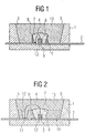
- FIG. 1 shown semiconductor device has a base body 1 a standard housing.
- This may be, for example, a surface-mountable LED housing that consists of a thermoplastic.
- the side walls 5 are slightly bevelled and act as a reflector for the generated radiation.
- a lead frame 2 is integrated.
- the semiconductor body 3 is bonded and electrically connected via a wire connection 4 with the wire terminal portion 11 of the lead frame 2.
- the contacting of the semiconductor body 3 can also take place via a plurality of wire connections.
- the semiconductor body 3 around a smaller reflector ring 6 is formed.
- a material for this reflector ring also a thermoplastic can be used.
- the reflector ring 6 is filled with the luminescence conversion element, which consists of a suspension of the phosphor 8 in a matrix such as silicone. Due to its aging stability, silicone is suitable in particular for the use of short-wave (blue, UV) emitting semiconductor bodies 3.
- the remaining part of the recess is filled with a transparent encapsulation 13 such as epoxy resin.
- the semiconductor device shown differs from that in FIG. 1 shown component in that the area around the semiconductor body 3 for receiving the luminescence conversion element 7 is formed by a recess over the chip terminal region 12 of the lead frame 2.
- the leadframe 2 is covered by a thin molding compound layer 10 (preferably also 0.3 mm to 0.7 mm in height), the depression being formed by a recess of the molding compound layer 10 over the chip connection region 12.
- a thin molding compound layer 10 preferably also 0.3 mm to 0.7 mm in height
- the depression being formed by a recess of the molding compound layer 10 over the chip connection region 12.
- an embodiment of the recess with sharp edges 9 for forming a dome of the luminescence conversion element 7 over the semiconductor body 3 may be advantageous.
- the recessed area of the molding compound around the semiconductor body 3 is filled with the luminescence conversion element 7.
- the wire connection region 11 is recessed from the molding compound layer 10.
- This recess is designed so that the side surfaces the recess of the housing side surfaces 5 are discontinued. This prevents parts of the phosphor suspension, which can penetrate into the recess above the wire connection region 11 during manufacture, from flowing up to the housing wall 5. This upflow is promoted inter alia by the roughness of the housing wall 5 and is undesirable, since thereby the emission range of the fluorescent light is increased.
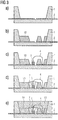
- FIG. 3 is shown schematically an example of a non-inventive manufacturing method.
- the base body 1 is produced with a recess and integrated lead frame 2, FIG. 3a ,
- the base body 1 is produced with a recess and integrated lead frame 2, FIG. 3a ,
- the lead frame 2 is produced with the housing molding compound in an injection molding process.
- the lead frame 2 is over-molded with the molding compound, for example PPA, so that the lead frame 2 is covered by a molding compound layer 10 of constant thickness.
- the chip connection region 12 and the wire connection region 11 of the leadframe 2 are kept free, FIG. 3b , Alternatively, the in FIG. 3b Of course, shown housing form can also be produced in a single process step.
- the semiconductor body 3 is bonded to the chip connection region 12 and the wire connection 4 is produced between the semiconductor body 3 and the lead frame 2, Figure 3c .
- the recess is filled around the semiconductor body 3 with the luminescence conversion element 7, for example a suspension of a phosphor in a synthetic resin, 3d figure ,
- a potting 13 of the device with a radiation-transparent material such as epoxy resin, FIG. 3e Depending on the requirements of the component the surface of the potting can be flat, lenticular, napped or run as a diffuser.
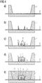
- the base body 1 is also produced in the first step with recess and embedded lead frame 2, FIG. 4a ,
- a reflector ring 6 surrounding the chip connection region 12 is sprayed onto the lead frame 2, FIG. 4b , Again, the production of the main body 1 and the reflector ring 6 can be carried out in a single manufacturing step.
- the semiconductor body 3 is then mounted on the chip terminal region 12 of the leadframe 2 and contacted, Figure 4c .
- the reflector ring 6 is filled with the luminescence conversion element 7 in the form of a phosphor suspension, a dome being formed above the semiconductor body 3 due to the sharp-edged boundary 9 of the reflector ring 6 and the surface tension of the phosphor suspension, FIG. 4d , As a result, a complete enclosure of the semiconductor body 3 is ensured without unnecessarily increasing the volume of the luminescence conversion element 7.
- the device can then be cast, Figure 4e ,
Description
Die Erfindung bezieht sich auf ein strahlungsemittierendes Halbleiterbauelement nach dem Oberbegriff des Patentanspruchs 1 sowie ein Herstellungsverfahren hierfür nach dem Oberbegriff des Patentanspruchs 18. Stahlungsemittierende Halbleiterbauelemente sind beispielsweise aus
Solche Bauelemente enthalten einen Halbleiterkörper, der im Betrieb Licht aussendet (Primärlicht) und ein Lumineszenzkonversionselement, das einen Teil dieses Lichts in einen anderen Wellenlängenbereich konvertiert (Fluoreszenzlicht). Der Gesamtfarbeindruck des von einem solchen Halbleiterbauelement emittierten Lichts ergibt sich durch additive Farbmischung aus Primärlicht und Fluoreszenzlicht.Such devices include a semiconductor body that emits light in operation (primary light) and a luminescence conversion element that converts a portion of this light into another wavelength range (fluorescent light). The overall color impression of the light emitted by such a semiconductor component results from additive color mixing of primary light and fluorescent light.
Häufig wird als Lumineszenzkonversionselement ein Leuchtstoff verwendet, der in einem Kunstharz suspendiert ist. Wie in
Diese Anordnung besitzt den Nachteil, daß die Quellen von Primärlicht - Halbleiterkörper - und von Fluoreszenzlicht - Leuchtstoffsuspension - im allgemeinen von verschiedener Form und Größe sind, so daß je nach Abstrahlrichtung eine Aufspaltung in verschiedene Farbanteile erfolgt und ein räumlich inhomogener Farbeindruck entsteht. Bei optischen Abbildungen treten starke chromatische Fehler auf.This arrangement has the disadvantage that the sources of primary light - semiconductor body - and of fluorescent light - phosphor suspension - are generally of different shape and size, so that depending on the direction of radiation splitting takes place in different color components and a spatially inhomogeneous Color impression arises. Optical images show strong chromatic errors.
Ein weiterer Nachteil besteht darin, daß der Farbeindruck von der optischen Weglänge in der Suspension abhängt, so daß fertigungsbedingte Schwankungen der Dicke der Suspensionsschicht über dem Halbleiterkörper zu verschiedenen Farbeindrücken führen. Ferner ist grundsätzlich eine sehr gleichmäßige Verteilung des Leuchtstoffs in der Suspension nötig.Another disadvantage is that the color impression depends on the optical path length in the suspension, so that production-related fluctuations in the thickness of the suspension layer over the semiconductor body lead to different color impressions. Furthermore, a very uniform distribution of the phosphor in the suspension is basically necessary.
Der vorliegenden Erfindung liegt die Aufgabe zugrunde, ein strahlungsemittierendes Halbleiterbauelement der eingangs genannten Art zu entwickeln, das homogen mischfarbiges Licht abstrahlt. Weiterhin ist es Aufgabe der vorliegenden Erfindung, ein Herstellungsverfahren für solche Bauelemente zu schaffen.The present invention has for its object to develop a radiation-emitting semiconductor device of the type mentioned, which radiates homogeneous mixed-colored light. It is another object of the present invention to provide a manufacturing method for such components.
Diese Aufgabe wird durch ein Halbleiterbauelement nach Patentanspruch 1 sowie ein Verfahren nach Patentanspruch 18 gelöst. Vorteilhafte Weiterbildungen der Erfindung sind Gegenstand der abhängigen Ansprüche.This object is achieved by a semiconductor device according to
Erfindungsgemäß ist vorgesehen, den Grundkörper des Halbleiterbauelements so auszuführen, daß in der zur Aufnahme des Halbleiterkörpers gebildeten Ausnehmung in der unmittelbaren Umgebung des Halbleiterkörpers ein gesonderter, napfförmiger Bereich ausgeformt ist, der das Lumineszenzkonversionselement enthält. Gegenüber einer großvolumigen, die gesamte Ausnehmung füllenden Umhüllung des Halbleiterkörpers mit dem Lumineszenzkonversionselement besitzt diese Anordnung den Vorteil, daß das Fluoreszenzlicht aus nahezu demselben Volumen wie das Primärlicht abgestrahlt wird, wodurch ein besonders gleichmäßiger Farbeindruck entsteht.According to the invention, the main body of the semiconductor component is designed so that a separate, cup-shaped region is formed in the recess formed for receiving the semiconductor body in the immediate vicinity of the semiconductor body, which contains the luminescence conversion element. Compared to a large-volume, the entire recess filling sheath of the semiconductor body with the luminescence conversion element, this arrangement has the advantage that the fluorescent light from almost the same volume as the primary light is emitted, creating a particularly uniform color impression.
Bei einer nicht erfindungsgemäßen Ausführungsform ist der gesonderte Bereich zur Aufnahme des Lumineszenzkonversionselements durch eine Vertiefung innerhalb der Ausnehmung geformt.In a non-inventive embodiment, the separate area for receiving the Lumineszenzkonversionselements formed by a recess within the recess.
Erfindungsgemäß ist der gesonderte Bereich durch eine ringförmige Einfassung auf dem Grund der Ausnehmung ausgebildet. Hierbei können mit großem Vorteil Gehäuse mit Standardformen als Grundkörper verwendet werden.According to the invention, the separate area is formed by an annular enclosure on the bottom of the recess. In this case, housing with standard shapes can be used as a basic body with great advantage.
Die Seitenflächen der ringförmigen Einfassung sind so geformt, daß die Seitenflächen als Reflektor für die erzeugte Strahlung dienen und so die Strahlungsausbeute erhöht wird.The side surfaces of the annular enclosure are shaped so that the side surfaces serve as a reflector for the generated radiation and thus the radiation efficiency is increased.
Eine vorteilhafte Weiterbildung der Erfindung besteht darin, daß in den Grundkörper ein Leiterrahmen so eingebettet ist, daß auf dem Leiterrahmen die ringförmige Einfassung geformt ist. Der Halbleiterkörper ist bei dieser Weiterbildung auf dem Leiterrahmen angebracht, wobei die elektrische Kontaktierung direkt (chip bonding) oder mittels Drahtverbindung (wire bonding) hergestellt sein kann. Diese sogenannte Leiterrahmentechnik wird vielfach bei strahlungsemittierenden Halbleiterbauelementen angewandt und kann mit Vorteil auch bei der vorliegenden Erfindung eingesetzt werden.An advantageous development of the invention is that in the base body, a lead frame is embedded so that the annular frame is formed on the lead frame. The semiconductor body is mounted in this development on the lead frame, wherein the electrical contact can be made directly (chip bonding) or by means of wire bonding (wire bonding). This so-called ladder frame technique is widely used in radiation-emitting semiconductor devices and can be used with advantage in the present invention.
Zum Schutz des Halbleiterkörpers und des Lumineszenzkonversionselements kann die Ausnehmung mit einer strahlungsdurchlässigen Füllmasse, beispielsweise einer Vergußmasse, gefüllt sein. Vorzugsweise enthält diese Füllmasse ein Reaktionsharz, beispielsweise ein Acrylharz, ein Epoxidharz, ein Silikonharz oder eine Mischung dieser Harze. Durch eine geeignete Formgebung der Füllmasse kann eine Linsenwirkung oder eine Streuwirkung erzielt werden, die die Abstrahlungseigenschaften des erfindungsgemäßen Bauelements weiter verbessert oder wunschgemäß modifiziert. Auch kann es für automatische Bestückungsanlagen von Vorteil sein, mittels der Füllmasse bei dem Bauelement eine plane Oberfläche auszubilden, da solche Bauelemente von Bestückungsautomaten leichter aufgenommen und positioniert werden können (pick and place-Verfahren).To protect the semiconductor body and the luminescence conversion element, the recess may be filled with a radiation-permeable filling compound, for example a potting compound. Preferably, this filler contains a reaction resin, for example an acrylic resin, an epoxy resin, a silicone resin or a mixture of these resins. By means of a suitable shaping of the filling compound, a lens effect or a scattering effect can be achieved which further improves the radiation properties of the component according to the invention or modifies it as desired. Also, it may be advantageous for automatic placement systems, by means of the filling compound in the device form a flat surface, since such components of pick and place machines can be easily taken and positioned (pick and place method).
Bei einer aufgrund besonders einfacher Realisierbarkeit bevorzugten Ausführungsform besteht das Lumineszenzkonversionselement aus einem oder mehreren Leuchtstoffen, die in eine Matrix eingebettet sind. Als Matrix eignen sich hinsichtlich Mischbarkeit, Formbarkeit und Handhabung besonders Acrylharze, Epoxidharze und Silikonharze sowie Mischungen hiervon.In an embodiment that is particularly easy to implement, the luminescence conversion element consists of one or more phosphors embedded in a matrix. Acrylic resins, epoxy resins and silicone resins and mixtures thereof are particularly suitable as matrices for miscibility, moldability and handling.
Als Leuchtstoff können einerseits organische Verbindungen wie beispielsweise Perylenfarbstoffe oder 4f-metallorganische Verbindungen eingemischt werden. So lassen sich Leuchtstoffe wie BASF Lumogen F083, Lumogen F240 und Lumogen F300 auf einfache Weise transparentem Epoxidharz zusetzen.On the one hand, organic compounds such as, for example, perylene dyes or 4f-organometallic compounds can be mixed in as the phosphor. For example, phosphors such as BASF Lumogen F083, Lumogen F240 and Lumogen F300 can be easily added to transparent epoxy resin.
Ein weißer Gesamtfarbeindruck kann durch Verwendung von anorganischen Leuchtstoffen erreicht werden. Hierfür eigen sich insbesondere mit Seltenen Erden dotierte Granate sowie mit Seltenen Erden dotierte Erdalkalisulfide.A white overall color impression can be achieved by using inorganic phosphors. Particularly suitable for this purpose are rare earth-doped grenades and rare earth-doped alkaline earth sulfides.
Effiziente Leuchtstoffe sind hierbei Verbindungen, die der Formel A3B5O12:M genügen (sofern sie nicht unter den üblichen Herstellungs- und Betriebsbedingungen instabil sind). Darin bezeichnet A mindestens ein Element der Gruppe Y, Lu, Sc, La, Gd, Tb und Sm, B mindestens ein Element der Gruppe Al, Ga und In und M mindestens ein Element der Gruppe Ce und Pr, vorzugsweise Ce. Besonders bevorzugt sind hierbei als Leuchtstoff YAG:Ce (Y3Al5O12:Ce3+), TbYAG:Ce ((YxTb1-x)3Al5O12:Ce3+, 0≤x≤1), GdYAG:Ce ((GdxY1-x)3Al5O12:Ce3+, 0<x<1), GdTbYAG:Ce ((GdxTbyY1-x-y)3Al5O12:Ce3, 0<x<1, 0<y<1) sowie hierauf basierende Gemische. Dabei kann Al zumindest teilweise durch Ga oder In ersetzt sein. Weiter bevorzugt sind die Verbindungen SrS:Ce3+, Na, SrS: Ce3+, Cl, SrS:CeCl3, CaS:Ce3+, SrSe:Ce3+ und Y3Ga5O12:Ce3+.Efficient phosphors here are compounds which satisfy the formula A 3 B 5 O 12 : M (unless they are unstable under the usual conditions of manufacture and operation). A denotes at least one element of the group Y, Lu, Sc, La, Gd, Tb and Sm, B at least one element of the group Al, Ga and In and M at least one element of the group Ce and Pr, preferably Ce. YAG: Ce (Y 3 Al 5 O 12 : Ce 3+ ), TbYAG: Ce ((Y x Tb 1-x ) 3 Al 5 O 12 : Ce 3+ , 0≤x≤1) are particularly preferred here. , GdYAG: Ce ((Gd x Y 1-x ) 3 Al 5 O 12 : Ce 3+ , 0 <x <1), GdTbYAG: Ce ((Gd x Tb y Y 1-xy ) 3 Al 5 O 12 : Ce 3 , 0 <x <1, 0 <y <1) and mixtures based thereon. In this case, Al may at least partially be replaced by Ga or In. More preferably, the compounds SrS: Ce 3+ , Na, SrS: Ce 3+ , Cl, SrS: CeCl 3 , CaS: Ce 3+ , SrSe: Ce 3+, and Y 3 Ga 5 O 12 : Ce 3+ .
Zur Erzeugung von verschiedenartig mischfarbigem Licht eignen sich mit Seltenen Erden dotierte Thiogallate wie beispielsweise CaGa2S4:Ce3+ oder SrGa2S4:Ce3+. Ebenso ist hierzu die Verwendung von mit Seltenen Erden dotierten Aluminaten wie beispielsweie YAlO3:Ce3+ und YAl1-xGaxO3:Ce3+, 0≤x≤1 und mit Seltenen Erden dotierten Orthosilikaten M'2SiO5:Ce3+ (M':Sc,Y,La) wie beispielsweise Y2SiO5:Ce3+ denkbar. Bei allen Yttriumverbindungen kann Yttrium im Prinzip durch Scandium oder Lanthan ersetzt werden. Die jeweilige Zusammensetzung des Leuchtstoffs bestimmt sich dabei in erster Linie aus dem gewünschten Gesamtfarbeindruck sowie der Zentralwellenlängen des Primärlichts.For producing mixed-colored light, rare-earth-doped thiogallates such as, for example, CaGa 2 S 4 : Ce 3+ or SrGa 2 S 4 : Ce 3+ are suitable. The use of rare earth doped aluminates such as YAlO 3 : Ce 3+ and YAl 1-x Ga x O 3 : Ce 3+ , 0≤x≤1 and rare earth doped orthosilicates M ' 2 SiO 5 : Ce 3+ (M ': Sc, Y, La) such as Y 2 SiO 5 : Ce 3+ conceivable. For all yttrium compounds, yttrium can in principle be replaced by scandium or lanthanum. The particular composition of the phosphor is determined primarily by the desired overall color impression and the central wavelengths of the primary light.
Bei einer weiteren besonders bevorzugten Ausführungsform werden als Matrix für das Lumineszenzkonversionselement und als Füllmasse in der Ausnehmung verschiedene Materialien verwendet. Dabei kann mit Vorteil für das Lumineszenzkonversionselement ein Material verwendet werden, daß hinsichtlich Mischbarkeit mit dem Leuchtstoff und Strahlungsbeständigkeit optimal ist, während für die Füllmasse ein Material gewählt wird, das sich aufgrund seiner Transparenz und seiner mechanischen Beständigkeit besonders eignet.In a further particularly preferred embodiment, different materials are used as matrix for the luminescence conversion element and as filling compound in the recess. It can be used with advantage for the luminescence conversion element, a material that is optimal in terms of miscibility with the phosphor and radiation resistance, while a material is selected for the filling material, which is particularly suitable due to its transparency and its mechanical resistance.
Durch diese zusätzliche Variationsmöglichkeit bei der Wahl der Füllmasse und Matrix des Lumineszenzkonversionselements können so vorteilhafterweise weitere Randbedingungen bei der Gestaltung eines strahlungsemittierenden Halbleiterbauelements mit Lumineszenzkonversionselement erfüllt werden.As a result of this additional possibility of variation in the choice of the filling compound and matrix of the luminescence conversion element, further boundary conditions can advantageously be fulfilled in the design of a radiation-emitting semiconductor component with a luminescence conversion element.
Mit besonderem Vorteil können bei erfindungsgemäßen Bauelementen Halbleiterkörper verwendet werden, die Licht mit einer Zentralwellenlänge unter 460 nm abstrahlen. Die Verwendung solcher Halbleiterkörper ist bei den oben beschriebenen Bauelementen nach dem Stand der Technik nicht sinnvoll, da Licht in diesem Wellenlängenbereich die Füllmasse schädigen kann, so daß die Füllmasse dadurch sehr schnell altert. Dieser Nachteil ist bei erfindungsgemäßen Bauelementen gemindert, da ein Teil der Primärstrahlung sehr nahe am Halbleiterkörper konvertiert wird, so daß der Anteil der kurzwelligen Strahlung in der Füllmasse reduziert ist und insgesamt die Lebensdauer des Bauelements verlängert wird.Semiconductor bodies which emit light having a central wavelength of less than 460 nm can be used to particular advantage in devices according to the invention. The use of such semiconductor body is not useful in the above-described prior art devices, since light in this wavelength range can damage the filling material, so that the filling material ages very quickly. This disadvantage is mitigated in components according to the invention, since a portion of the primary radiation is converted very close to the semiconductor body, so that the proportion of short-wave radiation is reduced in the filling material and overall the life of the device is extended.
Bevorzugt wird als Matrix für das Lumineszenzkonversionselement ein Silikonharz verwendet, das sich durch eine besonders hohe Strahlungsbeständigkeit im grünen, blauen und ultravioletten Spektralbereich auszeichnet. Die Verwendung von Silikonharzen ist besonders vorteilhaft in Verbindung mit Halbleiterkörper, die Strahlung mit einer Wellenlänge unter 430 nm emittieren. Strahlung in diesem Spektralbereich kann bei anderen Harzen zu Strahlungsschäden führen, die die Lebensdauer des Bauelements deutlich reduzieren. Ein Lumineszenzkonversionselement mit einer Silikonharzmatix kann bei der Erfindung mit einer das Lumineszenzkonversionselement abdekkenden Füllmasse auf des Basis eines Epoxidharzes kombiniert werden. Epoxidharze zeichnen sich hierbei durch hohe Transparenz und mechanische Stabilität aus.Preferably, a silicone resin is used as the matrix for the luminescence conversion element, which is characterized by a particularly high radiation resistance in the green, blue and ultraviolet spectral range. The use of silicone resins is particularly advantageous in conjunction with semiconductor bodies that emit radiation having a wavelength below 430 nm. Radiation in this spectral range can cause radiation damage to other resins, significantly reducing the life of the device. In the invention, a luminescence conversion element with a silicone resin matrix can be combined with a filling compound covering the luminescence conversion element based on an epoxy resin. Epoxy resins are characterized by high transparency and mechanical stability.
Mit besonderem Vorteil lassen sich mit erfindungsgemäßen Bauteilen Weißlichtleuchtdioden realisieren, wie sie in der oben genannten Druckschrift
Eine Mehrzahl von beanspruchten Bauelementen kann zu größeren Beleuchtungseinheiten zusammengefügt werden. Solche Beleuchtungseinheiten, gegebenenfalls mit matrixartiger Anordnung der Bauelemente, zeichnen sich durch hohe Leuchtdichte und besonders homogenen Gesamtfarbeindruck aus.A plurality of claimed components can be assembled into larger lighting units. Such lighting units, optionally with matrix-like arrangement of the components, are characterized by high luminance and particularly homogeneous overall color impression.
Mit besonderem Vorteil eignen sich die erfindungsgemäßen Bauelemente als Lichtquellen in abbildenden Linsensystemen. Da Primär- und Fluoreszenzlicht aus räumlich eng benachbarten und etwa gleich großen Volumina abgestrahlt werden, sind die chromatischen Verzerrungen, die ein solches Linsensystem hervorruft, deutlich geringer als bei Lichtquellen nach dem oben genannten Stand der Technik. Weiterhin ist es daher vorteilhafterweise möglich, die Abstrahlungscharakteristik eines erfindungsgemäßen Bauelements mittels einer oder mehrerer Linsen ohne Veränderung des Gesamtfarbeindrucks zu modifizieren.With particular advantage, the components of the invention are suitable as light sources in imaging lens systems. Since primary and fluorescent light are emitted from spatially closely spaced and approximately equally large volumes, the chromatic distortions that cause such a lens system, are significantly lower than in the light sources according to the above-mentioned prior art. Furthermore, it is therefore advantageously possible to modify the radiation characteristic of a component according to the invention by means of one or more lenses without changing the overall color impression.
Ausgangspunkt eines nicht erfindungsgemäßen Herstellungsverfahrens für ein strahlungsemittierendes Halbleiterbauelement mit Lumineszenzkonversionselement stellt ein Grundkörper mit einer Ausnehmung dar, in dem ein Leiterrahmen eingebettet ist, so daß ein Teilbereich des Leiterrahmens die Bodenfläche der Ausnehmung bildet. Zunächst wird der Leiterrahmen mit einer Formmasse überspritzt, wobei der Chipanschlußbereich ausgespart wird. Diese Aussparung bildet den gesonderten Bereich zur Aufnahme des Lumineszenzkonversionselements. Danach wird der Halbleiterkörper auf den Chipanschlußbereich des Leiterrahmens montiert und es werden die für den Betrieb erforderlichen elektrischen Verbindungen zwischen Halbleiterkörper und Leiterrahmen hergestellt. Im nächsten Schritt wird der ausgesparte Bereich mit dem Lumineszenzkonversionselement gefüllt, wobei der Halbleiterkörper vollständig in das Lumineszenzkonversionselement eingebettet wird.The starting point of a non-inventive manufacturing method for a radiation-emitting semiconductor device with Lumineszenzkonversionselement represents a base body with a recess in which a lead frame is embedded, so that a portion of the lead frame forms the bottom surface of the recess. First, the lead frame is over-molded with a molding compound, thereby recessing the chip terminal portion. This recess forms the separate area for receiving the luminescence conversion element. Thereafter, the semiconductor body is mounted on the chip terminal region of the lead frame and the necessary for the operation of electrical connections between the semiconductor body and lead frame are made. In the next step, the recessed area is filled with the luminescence conversion element, wherein the semiconductor body is completely embedded in the luminescence conversion element.
Bei einem erfindungsgemäßen Herstellungsverfahren wird ebenfalls als Ausgangsprodukt ein Grundkörper mit Ausnehmung verwendet, in dem ein Leiterrahmen so eingebettet ist, daß ein Teil des Leiterrahmens die Bodenfläche der Ausnehmung bildet. Auf dem Leiterrahmen wird um den Chipanschlußbereich herum mit einer Formmasse eine ringförmige Einfassung ausgebildet. Der Innenbereich dieser Einfassung bildet den gesonderten Bereich zur Aufnahme des Lumineszenzkonversionselements. Innerhalb dieser Einfassung wird auf dem Chipanschlußbereich des Leiterrahmens der Halbleiterkörper aufgebracht und es werden die für den Betrieb erforderlichen elektrischen Verbindungen zwischen Halbleiterkörper und Leiterrahmen hergestellt. Im nächsten Schritt wird die Einfassung mit dem Lumineszenzkonversionselement ausgefüllt, wobei der Halbleiterkörper vollständig in das Lumineszenzkonversionselement eingebettet wird. Dieses Verfahren besitzt den Vorteil, daß als Ausgangsmaterial Standardgehäuse beziehungsweise Grundkörper mit Standardgehäuseformen verwendet werden können. Die Ausformung des gesonderten Bereichs zur Aufnahme des Lumineszenzkonversionselements kann leicht in dem Herstellungsprozeß des erfindungsgemäßen Bauelements integriert werden.In a manufacturing method according to the invention, a base body with a recess is also used as the starting product, in which a lead frame is embedded so that a part of the lead frame forms the bottom surface of the recess. On the lead frame, an annular skirt is formed around the chip terminal region with a molding compound. The interior of this enclosure forms the separate area for receiving the luminescence conversion element. Within this enclosure, the semiconductor body is applied to the chip connection region of the leadframe and the electrical connections between semiconductor body and leadframe required for the operation are produced. In the next step, the enclosure is filled with the luminescence conversion element, wherein the semiconductor body is completely embedded in the luminescence conversion element. This method has the advantage that standard housing or base body with standard housing shapes can be used as the starting material. The shape of the separate area for receiving the luminescence conversion element can be easily integrated in the manufacturing process of the device according to the invention.
Bei einer vorteilhaften Weitergestaltung der Erfindung wird die Ausnehmung mit einer strahlungsdurchlässigen Füllmasse, beispielsweise einer entsprechenden Vergußmasse, gefüllt. Da die Umhüllung des Halbleiterkörpers in zwei Schritten erfolgt, werden vorteilhafterweise Delamination des Halbleiterkörpers von der Umhüllung und Rissbildung in der Umhüllung vermindert und dadurch Feuchtebeständigkeit und Lebensdauer des Bauelements erhöht.In an advantageous further embodiment of the invention, the recess is filled with a radiation-permeable filling compound, for example a corresponding potting compound. Since the cladding of the semiconductor body takes place in two steps, advantageously delamination of the semiconductor body from the cladding and crack formation in the cladding is reduced, thereby increasing the moisture resistance and the lifetime of the component.
Weitere Merkmale und Vorteile ergeben sich aus der nachfolgenden Beschreibung von vier Ausführungsbeispielen in Verbindung mit den
Es zeigen:
-
Figur 1 -
Figur 2 -
Figur 3 -
Figur 4
-
FIG. 1 a schematic sectional view of an embodiment of a radiation-emitting semiconductor device according to the invention with luminescence conversion element, -
FIG. 2 FIG. 2 shows a schematic sectional view of an example of a non-inventive radiation-emitting semiconductor component with luminescence conversion element, FIG. -
FIG. 3 a schematic representation of an example of a non-inventive manufacturing method and -
FIG. 4 a schematic representation of an embodiment of a manufacturing method according to the invention.
In den verschiedenen Figuren sind gleiche beziehungsweise gleichwirkende Teile mit demselben Bezugszeichen versehen.In the various figures, identical or equivalent parts are provided with the same reference numeral.
Das in
Um den Halbleiterkörper 3 herum ist ein kleinerer Reflektorring 6 ausgebildet. Vorzugsweise kann als Material für diesen Reflektorring ebenfalls ein Thermoplast verwendet werden. Der Reflektorring 6 ist mit dem Lumineszenzkonversionselement gefüllt, das aus einer Suspension des Leuchtstoffs 8 in einer Matrix wie beispielsweise Silikon besteht. Silikon eignet sich aufgrund seiner Alterungsstabilität insbesondere bei der Verwendung kurzwellig (blau, UV) emittierender Halbleiterkörper 3.Around the
Als Bauhöhe des Reflektorrings 6 haben sich Maße zwischen 0,3 mm und 0,7 mm als besonders vorteilhaft erwiesen. Reflektoren dieser Größe gewährleisten einerseits eine vollständige Einhüllung des Halbleiterkörpers 3 mit dem Lumineszenzkonversionselement 7, ohne andererseits das Volumen des Lumineszenzkonversionselements 7 unnötig zu vergrößern.As a height of the
Hierbei ist es von besonderem Vorteil, den Reflektorring 6 mit scharfen Kanten 9 auszubilden. Dies bewirkt, daß bei der Befüllung des Reflektorrings 6 die Leuchtstoffsuspension aufgrund ihrer Oberflächenspannung eine Kuppe über dem Reflektorring 6 ausbildet, wodurch weitergehend die vollständige Einbettung des Halbleiterkörpers 3 in das Lumineszenzkonversionselement 7 sichergestellt wird.It is of particular advantage to form the
Der verbleibende Teil der Ausnehmung ist mit einem transparentem Verguß 13 wie beispielsweise Epoxidharz gefüllt.The remaining part of the recess is filled with a
Das in
Bei dem gezeigten Beispiel ist weiterhin der Drahtanschlußbereich 11 von der Formmasseschicht 10 ausgespart. Diese Aussparung ist so gestaltet, daß die Seitenflächen der Aussparung von den Gehäuseseitenflächen 5 abgesetzt sind. Dies verhindert, daß Teile der Leuchtstoffsuspension, die bei der Herstellung in die Aussparung über dem Drahtanschlußbereich 11 eindringen können, an der Gehäusewand 5 hinauffließen. Dieses Hinauffließen wird unter anderem durch die Rauhigkeit der Gehäusewand 5 begünstigt und ist unerwünscht, da dadurch der Abstrahlungsbereich des Fluoreszenzlichts vergrößert wird.In the example shown, furthermore, the
In
Im ersten Schritt wird der Grundkörper 1 mit Ausnehmung und intergriertem Leiterrahmen 2 hergestellt,
Im nächsten Schritt wird der Leiterrahmen 2 mit der Formmasse, beispielsweise PPA, überspritzt, so daß der Leiterrahmen 2 von eine Formmasseschicht 10 mit gleichbleibender Dicke abgedeckt wird. Der Chipanschlußbereich 12 und der Drahtanschlußbereich 11 des Leiterrahmens 2 wird dabei freigehalten,
Daraufhin wird der Halbleiterkörper 3 auf den Chipanschlußbereich 12 gebondet und die Drahtverbindung 4 zwischen Halbleiterkörper 3 und Leiterrahmen 2 hergestellt,
Abschließend kann ein Verguß 13 des Bauelements mit einem strahlungsdurchlässigen Material wie beispielsweise Epoxidharz erfolgen,
Bei dem in
Danach wird ein den Chipanschlußbereich 12 umgebender Reflektorring 6 auf den Leiterrahmen 2 aufgespritzt,
Der Halbleiterkörper 3 wird daraufhin auf den Chipanschlußbereich 12 des Leiterrahmens 2 montiert und kontaktiert,
Wie im vorangegangenen Beispiel kann danach das Bauelement vergossen werden,
Die Erläuterung der Erfindung anhand der oben beschriebenen Ausführungsbeispiele ist natürlich nicht als Beschränkung der Erfindung zu verstehen.The explanation of the invention with reference to the embodiments described above is of course not to be understood as limiting the invention.
Claims (23)
- Radiation-emitting semiconductor component having a basic body (1), at least one semiconductor body (3) and a luminescence conversion element (7), the basic body (1) having a recess, wherein
the recess comprises a bowl-like region in which the semiconductor body (3) is arranged and which is filled with the luminescence conversion element (7),
characterized in that
the bowl-like region is formed by an annular enclosure (6) on the base of the recess and the inner side surfaces of the annular enclosure serve as a reflector. - Radiation-emitting semiconductor component according to claim 1,
characterized in that
a leadframe (2) is embedded in the basic body (1) in such a way that a partial region of the leadframe (2) forms the bottom area of the depression. - Radiation-emitting semiconductor component according to claim 2,
characterized in that
a leadframe (2) is embedded in the basic body (1), such that a partial region of the leadframe (2) forms the bottom area of the recess and the annular enclosure (6) is formed on the leadframe (2). - Radiation-emitting semiconductor component according to one of the claims 1 to 3,
characterized in that
the basic body (1) is formed by injection molding or transfer molding. - Radiation-emitting semiconductor component according to one of the claims 1 to 4,
characterized in that
the luminescence conversion element (7) comprises an interface which seperates the bowl-like region from the remaining inner volume of the recess. - Radiation-emitting semiconductor component according to one of the claims 1 to 5,
characterized in that
the recess is filled at least partially with a radiation-transmissive potting (13) which borders the luminescence conversion element (7). - Radiation-emitting semiconductor component according to claim 6,
characterized in that
the potting (13) comprises a reaction resin. - Radiation-emitting semiconductor component according to claim 6 or 7,
characterized in that
the potting (13) comprises an acrylic resin, an epoxy resin, a silicone resin or a mixture of these resins. - Radiation-emitting semiconductor component according to claim 3,
characterized in that
the leadframe (2) has a chip connection region (12) and a wire connection region (11), and in that the semiconductor body is applied on the chip connection region (12) and is connected to the wire connection region (11) by a wire connection (4). - Radiation-emitting semiconductor component according to one of the claims 1 to 9,
characterized in that
the luminescence conversion element (7) contains at least one organic or inorganic phosphor embedded in a matrix. - Radiation-emitting semiconductor component according to claim 10,
characterized in that
the luminescence conversion element (7) contains YAG:Ce, TbYAG:Ce, GdYAG:Ce, GdTbYAG:Ce or mixtures based on these, where Al can be replaced at least in places by Ga or In. - Radiation-emitting semiconductor component according to claim 10 or 11,
characterized in that
the matrix comprises a reaction resin. - Radiation-emitting semiconductor component according to one of the claims 10 to 12,
characterized in that
the matrix comprises an acrylic resin, an epoxy resin, a silicone resin or a mixture of these resins. - Radiation-emitting semiconductor component according to one of the claims 10 to 13,
characterized in that
the filling of the recess and the matrix of the luminescence conversion element (7) comprise different materials. - Radiation-emitting semiconductor component according to one of the claims 10 to 14,
characterized in that
the recess is filled with a potting (13) which comprises an epoxy resin and the matrix comprises a silicone resin. - Radiation-emitting semiconductor component according to one of the claims 1 to 15,
characterized in that
the central wavelength of the radiation emitted by the semiconductor body (3) during operation lies below 460 nm. - Radiation-emitting semiconductor component according to one of the claims 1 to 16,
characterized in that
the color of the radiation emitted by the semiconductor body (3) during operation and the color of the light emitted by the luminescence conversion element (7) are complementary to one another, thereby giving rise to the impression of white light. - Method for producing a radiation-emitting semiconductor component with luminescence conversion element (7), characterized by the steps of- producing a basic body (1) with recess and embedded leadframe (2), which comprises a chip connection region (12),- forming an annular enclosure (6) on the base of the recess around the chip connection region (12) for forming a bowl-like region, where the inner side surfaces of the annular enclosure serve as a reflector for the emitted radiation,- applying a semiconductor body (3) in the bowl-like region to the chip connection region (12) and contact-connecting the semiconductor body (3),- filling the inner volume of the annular enclosure (6) with the luminescence conversion element (7).
- Method according to claim 18,
characterized in that
the bowl-like region is filled with the luminescence conversion element (7) in such a way that an interface of the luminescence conversion element (7) seperates the bowl-like region from the remaining inner volume of the recess. - Method according to claim 18 or 19,
characterized in that
the basic body (1) is formed by injection molding or transfer molding. - Method according to one of the claims 18 to 20,
characterized in that
the recess is filled with a radiation-transmissive potting (13) . - Use of one or of a plurality of radiation-emitting semiconductor components according to one of the claim 1 to 17 as a light source in an imaging optical system or in an LED illumination unit.
- Use of a plurality of radiation-emitting semiconductor components according to claim 22 in an LED illumination unit in which the radiation-emitting semiconductor components are arranged in matrixlike fashion.
Priority Applications (1)
| Application Number | Priority Date | Filing Date | Title |
|---|---|---|---|
| EP12166424.7A EP2485285A3 (en) | 2000-04-26 | 2001-04-26 | Light emitting semiconductor device with wavelength-converting element |
Applications Claiming Priority (3)
| Application Number | Priority Date | Filing Date | Title |
|---|---|---|---|
| DE10020465 | 2000-04-26 | ||
| DE10020465A DE10020465A1 (en) | 2000-04-26 | 2000-04-26 | Radiation-emitting semiconductor component with luminescence conversion element |
| PCT/DE2001/001601 WO2001082385A1 (en) | 2000-04-26 | 2001-04-26 | Radiation emitting semiconductor component with luminescence-converting element |
Related Child Applications (2)
| Application Number | Title | Priority Date | Filing Date |
|---|---|---|---|
| EP12166424.7A Division EP2485285A3 (en) | 2000-04-26 | 2001-04-26 | Light emitting semiconductor device with wavelength-converting element |
| EP12166424.7A Division-Into EP2485285A3 (en) | 2000-04-26 | 2001-04-26 | Light emitting semiconductor device with wavelength-converting element |
Publications (2)
| Publication Number | Publication Date |
|---|---|
| EP1277242A1 EP1277242A1 (en) | 2003-01-22 |
| EP1277242B1 true EP1277242B1 (en) | 2018-08-15 |
Family
ID=7640000
Family Applications (2)
| Application Number | Title | Priority Date | Filing Date |
|---|---|---|---|
| EP12166424.7A Withdrawn EP2485285A3 (en) | 2000-04-26 | 2001-04-26 | Light emitting semiconductor device with wavelength-converting element |
| EP01940201.5A Expired - Lifetime EP1277242B1 (en) | 2000-04-26 | 2001-04-26 | Radiation emitting semiconductor component with luminescence-converting element and method of manufacturing the same |
Family Applications Before (1)
| Application Number | Title | Priority Date | Filing Date |
|---|---|---|---|
| EP12166424.7A Withdrawn EP2485285A3 (en) | 2000-04-26 | 2001-04-26 | Light emitting semiconductor device with wavelength-converting element |
Country Status (7)
| Country | Link |
|---|---|
| US (3) | US6897490B2 (en) |
| EP (2) | EP2485285A3 (en) |
| JP (2) | JP5100944B2 (en) |
| CN (2) | CN1284249C (en) |
| DE (1) | DE10020465A1 (en) |
| TW (1) | TW533602B (en) |
| WO (1) | WO2001082385A1 (en) |
Families Citing this family (139)
| Publication number | Priority date | Publication date | Assignee | Title |
|---|---|---|---|---|
| KR100450647B1 (en) | 1999-07-23 | 2004-10-01 | 파텐트-트로이한트-게젤샤프트 퓌어 엘렉트리쉐 글뤼람펜 엠베하 | Luminescent array, wavelength-converting sealing material and light source |
| JP4817534B2 (en) * | 2000-06-09 | 2011-11-16 | 星和電機株式会社 | Light emitting diode lamp |
| DE10122002A1 (en) * | 2001-05-07 | 2002-11-21 | Osram Opto Semiconductors Gmbh | Housing for an optoelectronic component and optoelectronic component |
| US6616862B2 (en) | 2001-05-21 | 2003-09-09 | General Electric Company | Yellow light-emitting halophosphate phosphors and light sources incorporating the same |
| US6596195B2 (en) * | 2001-06-01 | 2003-07-22 | General Electric Company | Broad-spectrum terbium-containing garnet phosphors and white-light sources incorporating the same |
| DE10214119A1 (en) * | 2002-03-28 | 2003-10-23 | Osram Opto Semiconductors Gmbh | Optoelectronic component comprises a casting compound which lets through radiation and consist of silicone or a silicone resin |
| CN100338786C (en) * | 2002-06-19 | 2007-09-19 | 三垦电气株式会社 | Semiconductor light emitting device, method for producing the same and reflector for semiconductor light emitting device |
| TW200414572A (en) | 2002-11-07 | 2004-08-01 | Matsushita Electric Ind Co Ltd | LED lamp |
| JP2004186168A (en) * | 2002-11-29 | 2004-07-02 | Shin Etsu Chem Co Ltd | Silicone resin composition for light emitting diode element |
| US7595113B2 (en) | 2002-11-29 | 2009-09-29 | Shin-Etsu Chemical Co., Ltd. | LED devices and silicone resin composition therefor |
| DE20306928U1 (en) * | 2003-01-30 | 2004-06-03 | Osram Opto Semiconductors Gmbh | Semiconductor component emitting and/or receiving radiation used as an optoelectronic semiconductor component comprises a semiconductor chip arranged in a recess of a housing base body and encapsulated with a sleeve mass |
| TWI237546B (en) | 2003-01-30 | 2005-08-01 | Osram Opto Semiconductors Gmbh | Semiconductor-component sending and/or receiving electromagnetic radiation and housing-basebody for such a component |
| JP2004260620A (en) | 2003-02-26 | 2004-09-16 | Ntt Docomo Inc | Radio data communication method, server device, and radio controller |
| JP2004265979A (en) * | 2003-02-28 | 2004-09-24 | Noritsu Koki Co Ltd | Light emitting diode light source unit |
| WO2005015646A1 (en) | 2003-08-07 | 2005-02-17 | Matsushita Electric Industrial Co., Ltd. | Led illumination light source |
| AR045260A1 (en) | 2003-08-12 | 2005-10-19 | 3M Innovative Properties Co | COMPOUNDS CONTAINING IMIDAZO-OXIMA REPLACED |
| MXPA06002199A (en) | 2003-08-27 | 2006-05-22 | 3M Innovative Properties Co | Aryloxy and arylalkyleneoxy substituted imidazoquinolines. |
| WO2005023190A2 (en) | 2003-09-05 | 2005-03-17 | 3M Innovative Properties Company | Treatment for cd5+ b cell lymphoma |
| US7854535B2 (en) | 2003-09-23 | 2010-12-21 | Avago Technologies Ecbu Ip (Singapore) Pte. Ltd. | Ceramic packaging for high brightness LED devices |
| US20080025030A9 (en) * | 2003-09-23 | 2008-01-31 | Lee Kong W | Ceramic packaging for high brightness LED devices |
| US7544697B2 (en) | 2003-10-03 | 2009-06-09 | Coley Pharmaceutical Group, Inc. | Pyrazolopyridines and analogs thereof |
| US8871782B2 (en) | 2003-10-03 | 2014-10-28 | 3M Innovative Properties Company | Alkoxy substituted imidazoquinolines |
| US8598192B2 (en) | 2003-11-14 | 2013-12-03 | 3M Innovative Properties Company | Hydroxylamine substituted imidazoquinolines |
| CA2545774A1 (en) | 2003-11-14 | 2005-06-02 | 3M Innovative Properties Company | Oxime substituted imidazo ring compounds |
| CA2547020C (en) | 2003-11-25 | 2014-03-25 | 3M Innovative Properties Company | 1h-imidazo[4,5-c]pyridine-4-amine derivatives as immune response modifier |
| WO2005066170A1 (en) | 2003-12-29 | 2005-07-21 | 3M Innovative Properties Company | Arylalkenyl and arylalkynyl substituted imidazoquinolines |
| JP2007517044A (en) | 2003-12-30 | 2007-06-28 | スリーエム イノベイティブ プロパティズ カンパニー | Imidazoquinolinyl, imidazopyridinyl, and imidazonaphthyridinylsulfonamide |
| JP2005223112A (en) * | 2004-02-05 | 2005-08-18 | Citizen Electronics Co Ltd | Surface mounting light emitting diode |
| JP3892030B2 (en) | 2004-02-26 | 2007-03-14 | 松下電器産業株式会社 | LED light source |
| WO2005094531A2 (en) | 2004-03-24 | 2005-10-13 | 3M Innovative Properties Company | Amide substituted imidazopyridines, imidazoquinolines, and imidazonaphthyridines |
| JP4754850B2 (en) * | 2004-03-26 | 2011-08-24 | パナソニック株式会社 | Manufacturing method of LED mounting module and manufacturing method of LED module |
| US7517728B2 (en) * | 2004-03-31 | 2009-04-14 | Cree, Inc. | Semiconductor light emitting devices including a luminescent conversion element |
| US7326583B2 (en) * | 2004-03-31 | 2008-02-05 | Cree, Inc. | Methods for packaging of a semiconductor light emitting device |
| US7279346B2 (en) * | 2004-03-31 | 2007-10-09 | Cree, Inc. | Method for packaging a light emitting device by one dispense then cure step followed by another |
| DE102004021233A1 (en) | 2004-04-30 | 2005-12-01 | Osram Opto Semiconductors Gmbh | LED array |
| JP5366399B2 (en) | 2004-05-31 | 2013-12-11 | オスラム オプト セミコンダクターズ ゲゼルシャフト ミット ベシュレンクテル ハフツング | Optoelectronic semiconductor component and casing substrate for the component |
| US8017779B2 (en) | 2004-06-15 | 2011-09-13 | 3M Innovative Properties Company | Nitrogen containing heterocyclyl substituted imidazoquinolines and imidazonaphthyridines |
| WO2006065280A2 (en) | 2004-06-18 | 2006-06-22 | 3M Innovative Properties Company | Isoxazole, dihydroisoxazole, and oxadiazole substituted imidazo ring compounds and methods |
| US8026366B2 (en) | 2004-06-18 | 2011-09-27 | 3M Innovative Properties Company | Aryloxy and arylalkyleneoxy substituted thiazoloquinolines and thiazolonaphthyridines |
| WO2006038923A2 (en) | 2004-06-18 | 2006-04-13 | 3M Innovative Properties Company | Aryl substituted imidazonaphthyridines |
| EP1622237A1 (en) * | 2004-07-28 | 2006-02-01 | Infineon Technologies Fiber Optics GmbH | Electronic or optical device, and method implemented |
| US20060038198A1 (en) * | 2004-08-23 | 2006-02-23 | Chua Janet B Y | Device and method for producing output light having a wavelength spectrum in the visible range and the infrared range using a fluorescent material |
| EP1630913B1 (en) * | 2004-08-31 | 2007-10-03 | Infineon Technologies AG | Method for manufacturing an optical or electronic modul with a plastic casing containing an optical or electronic component as well as said optical or electronic modul |
| DE102004047640A1 (en) * | 2004-09-30 | 2006-04-13 | Osram Opto Semiconductors Gmbh | Optoelectronic component and housing for an optoelectronic component |
| US7679672B2 (en) * | 2004-10-14 | 2010-03-16 | Avago Technologies Ecbu Ip (Singapore) Pte. Ltd. | Electronic flash, imaging device and method for producing a flash of light having a wavelength spectrum in the visible range and the infrared range using a fluorescent material |
| US20060082995A1 (en) * | 2004-10-14 | 2006-04-20 | Chua Janet B Y | Device and method for producing output light having a wavelength spectrum in the infrared wavelength range and the visble wavelength range |
| DE102004053116A1 (en) * | 2004-11-03 | 2006-05-04 | Tridonic Optoelectronics Gmbh | Light-emitting diode arrangement with color conversion material |
| JP5313502B2 (en) | 2004-12-30 | 2013-10-09 | スリーエム イノベイティブ プロパティズ カンパニー | Substituted chiral condensed [1,2] imidazo [4,5-c] cyclic compounds |
| WO2006074003A2 (en) | 2004-12-30 | 2006-07-13 | 3M Innovative Properties Company | CHIRAL FUSED [1,2]IMIDAZO[4,5-c] RING COMPOUNDS |
| KR101047795B1 (en) * | 2005-01-05 | 2011-07-07 | 엘지이노텍 주식회사 | Semiconductor light emitting device |
| US7939842B2 (en) | 2005-01-27 | 2011-05-10 | Cree, Inc. | Light emitting device packages, light emitting diode (LED) packages and related methods |
| US9248127B2 (en) | 2005-02-04 | 2016-02-02 | 3M Innovative Properties Company | Aqueous gel formulations containing immune response modifiers |
| WO2006086634A2 (en) | 2005-02-11 | 2006-08-17 | Coley Pharmaceutical Group, Inc. | Oxime and hydroxylamine substituted imidazo[4,5-c] ring compounds and methods |
| CN100377376C (en) * | 2005-03-21 | 2008-03-26 | 亿光电子工业股份有限公司 | LED reflection cover manufacturing method |
| WO2006101174A1 (en) * | 2005-03-24 | 2006-09-28 | Kyocera Corporation | Light emitting element storing package, light emitting device and lighting apparatus |
| AU2006232375A1 (en) | 2005-04-01 | 2006-10-12 | Coley Pharmaceutical Group, Inc. | 1-substituted pyrazolo (3,4-c) ring compounds as modulators of cytokine biosynthesis for the treatment of viral infections and neoplastic diseases |
| US7943610B2 (en) | 2005-04-01 | 2011-05-17 | 3M Innovative Properties Company | Pyrazolopyridine-1,4-diamines and analogs thereof |
| KR100631993B1 (en) * | 2005-07-20 | 2006-10-09 | 삼성전기주식회사 | Led package and fabricating method thereof |
| US7365371B2 (en) * | 2005-08-04 | 2008-04-29 | Cree, Inc. | Packages for semiconductor light emitting devices utilizing dispensed encapsulants |
| US8835952B2 (en) | 2005-08-04 | 2014-09-16 | Cree, Inc. | Submounts for semiconductor light emitting devices and methods of forming packaged light emitting devices including dispensed encapsulants |
| US7646035B2 (en) * | 2006-05-31 | 2010-01-12 | Cree, Inc. | Packaged light emitting devices including multiple index lenses and multiple index lenses for packaged light emitting devices |
| US20070045800A1 (en) * | 2005-08-19 | 2007-03-01 | Brian King | Opto-coupler with high reverse breakdown voltage and high isolation potential |
| KR100780176B1 (en) * | 2005-11-25 | 2007-11-27 | 삼성전기주식회사 | Side-view light emitting diode package |
| US7772604B2 (en) | 2006-01-05 | 2010-08-10 | Illumitex | Separate optical device for directing light from an LED |
| US8044412B2 (en) | 2006-01-20 | 2011-10-25 | Taiwan Semiconductor Manufacturing Company, Ltd | Package for a light emitting element |
| US7777244B2 (en) | 2006-03-17 | 2010-08-17 | Seoul Semiconductor Co., Ltd. | Side-view light emitting diode package having a reflector |
| KR100875443B1 (en) | 2006-03-31 | 2008-12-23 | 서울반도체 주식회사 | Light emitting device |
| US8969908B2 (en) * | 2006-04-04 | 2015-03-03 | Cree, Inc. | Uniform emission LED package |
| US20070269915A1 (en) * | 2006-05-16 | 2007-11-22 | Ak Wing Leong | LED devices incorporating moisture-resistant seals and having ceramic substrates |
| US20070272934A1 (en) * | 2006-05-23 | 2007-11-29 | Kee Yean Ng | LED device with improved life performance |
| JP2009538536A (en) | 2006-05-26 | 2009-11-05 | クリー エル イー ディー ライティング ソリューションズ インコーポレイテッド | Solid state light emitting device and method of manufacturing the same |
| US7906506B2 (en) | 2006-07-12 | 2011-03-15 | 3M Innovative Properties Company | Substituted chiral fused [1,2] imidazo [4,5-c] ring compounds and methods |
| US20080035942A1 (en) * | 2006-08-08 | 2008-02-14 | Lg Electronics Inc. | Light emitting device package and method for manufacturing the same |
| US8367945B2 (en) * | 2006-08-16 | 2013-02-05 | Cree Huizhou Opto Limited | Apparatus, system and method for use in mounting electronic elements |
| DE102006046678A1 (en) | 2006-09-29 | 2008-04-03 | Osram Opto Semiconductors Gmbh | Housing for use with semiconductor body of e.g. LED unit, has plastic-base body with plastic components, where one plastic component is made of material differing from that of other component in optical characteristic |
| DE102006046301A1 (en) * | 2006-09-29 | 2008-04-03 | Osram Opto Semiconductors Gmbh | Optical element, has base body, which contains basic material, and filling body, which contains filling material, where filling body adheres to base body |
| JP2010506402A (en) | 2006-10-02 | 2010-02-25 | イルミテックス, インコーポレイテッド | LED system and method |
| US7808013B2 (en) * | 2006-10-31 | 2010-10-05 | Cree, Inc. | Integrated heat spreaders for light emitting devices (LEDs) and related assemblies |
| DE102006059994A1 (en) * | 2006-12-19 | 2008-06-26 | Osram Opto Semiconductors Gmbh | Optoelectronic semiconductor component |
| TWI326923B (en) * | 2007-03-07 | 2010-07-01 | Lite On Technology Corp | White light emitting diode |
| JP2008277607A (en) * | 2007-05-01 | 2008-11-13 | Matsushita Electric Ind Co Ltd | Light emitting device, linear light emitting device, surface light emitting device, liquid crystal display device and electronic equipment |
| US7915061B2 (en) * | 2007-05-31 | 2011-03-29 | GE Lighting Solutions, LLC | Environmentally robust lighting devices and methods of manufacturing same |
| US10505083B2 (en) * | 2007-07-11 | 2019-12-10 | Cree, Inc. | Coating method utilizing phosphor containment structure and devices fabricated using same |
| US9401461B2 (en) * | 2007-07-11 | 2016-07-26 | Cree, Inc. | LED chip design for white conversion |
| JP2009021426A (en) * | 2007-07-12 | 2009-01-29 | Sharp Corp | Chip component type led and method of manufacturing the same |
| DE102007042642A1 (en) * | 2007-09-07 | 2009-03-12 | Osram Gesellschaft mit beschränkter Haftung | Method for producing an optoelectronic component and optoelectronic component |
| US10256385B2 (en) | 2007-10-31 | 2019-04-09 | Cree, Inc. | Light emitting die (LED) packages and related methods |
| WO2009061859A2 (en) * | 2007-11-05 | 2009-05-14 | Hauptman-Woodward Medical Research Institute, Inc. | Protein crystal of human cytochrome p450 aromatase and uses thereof |
| DE102008003971A1 (en) * | 2008-01-11 | 2009-07-16 | Ledon Lighting Jennersdorf Gmbh | Light-emitting diode arrangement with protective frame |
| US7829358B2 (en) | 2008-02-08 | 2010-11-09 | Illumitex, Inc. | System and method for emitter layer shaping |
| US8877524B2 (en) * | 2008-03-31 | 2014-11-04 | Cree, Inc. | Emission tuning methods and devices fabricated utilizing methods |
| JP5207807B2 (en) * | 2008-04-14 | 2013-06-12 | シャープ株式会社 | Chip component type LED |
| CN101577300A (en) * | 2008-05-08 | 2009-11-11 | 先进开发光电股份有限公司 | Light-emitting diode (LED) and packaging method thereof |
| TWI475718B (en) * | 2008-05-21 | 2015-03-01 | Advanced Optoelectronic Tech | Light emitting diode and package method thereof |
| US8183585B2 (en) * | 2008-09-16 | 2012-05-22 | Osram Sylvania Inc. | Lighting module |
| US20100067240A1 (en) * | 2008-09-16 | 2010-03-18 | John Selverian | Optical Cup For Lighting Module |
| US8188486B2 (en) * | 2008-09-16 | 2012-05-29 | Osram Sylvania Inc. | Optical disk for lighting module |
| US8022626B2 (en) * | 2008-09-16 | 2011-09-20 | Osram Sylvania Inc. | Lighting module |
| JP2010123746A (en) * | 2008-11-19 | 2010-06-03 | Toshiba Corp | Optical semiconductor device, lighting device, and display device |
| JP4799606B2 (en) * | 2008-12-08 | 2011-10-26 | 株式会社東芝 | Optical semiconductor device and method for manufacturing optical semiconductor device |
| TW201034256A (en) | 2008-12-11 | 2010-09-16 | Illumitex Inc | Systems and methods for packaging light-emitting diode devices |
| TWI403006B (en) | 2009-01-15 | 2013-07-21 | Everlight Electronics Co Ltd | Light emitting diode and method for fabricating the same |
| TWI449221B (en) * | 2009-01-16 | 2014-08-11 | Everlight Electronics Co Ltd | Led packging structure and fabricating method thereof |
| CN101783379B (en) * | 2009-01-20 | 2011-08-24 | 亿光电子工业股份有限公司 | Element encapsulation structure of light-emitting diode and manufacturing method thereof |
| US8585253B2 (en) | 2009-08-20 | 2013-11-19 | Illumitex, Inc. | System and method for color mixing lens array |
| US8449128B2 (en) | 2009-08-20 | 2013-05-28 | Illumitex, Inc. | System and method for a lens and phosphor layer |
| DE102009055786A1 (en) | 2009-11-25 | 2011-05-26 | Osram Opto Semiconductors Gmbh | Housing, optoelectronic component and method for producing a housing |
| TW201128812A (en) | 2009-12-01 | 2011-08-16 | Lg Innotek Co Ltd | Light emitting device |
| JP5535750B2 (en) * | 2010-04-30 | 2014-07-02 | ローム株式会社 | Light emitting element module |
| KR101039994B1 (en) * | 2010-05-24 | 2011-06-09 | 엘지이노텍 주식회사 | Light emitting device and light unit having thereof |
| CN101859759A (en) * | 2010-06-03 | 2010-10-13 | 陕西科技大学 | White LED light source package |
| WO2011160676A1 (en) * | 2010-06-22 | 2011-12-29 | Osram Ag | Phosphor device and lighting apparatus comprising the same |
| KR101677105B1 (en) * | 2010-08-30 | 2016-11-17 | 삼성디스플레이 주식회사 | Electronic component and manufacturing method for the same |
| KR101761637B1 (en) * | 2010-11-24 | 2017-07-27 | 삼성전자주식회사 | Light emitting diode package and manufaturing method thereof |
| JP2014038876A (en) * | 2010-12-15 | 2014-02-27 | Panasonic Corp | Semiconductor light-emitting device |
| JP5582048B2 (en) * | 2011-01-28 | 2014-09-03 | 日亜化学工業株式会社 | Light emitting device |
| KR101847938B1 (en) * | 2011-03-14 | 2018-04-13 | 삼성전자주식회사 | Light emitting device package and manufacturing method thereof |
| CN102694102B (en) * | 2011-03-22 | 2014-11-05 | 展晶科技(深圳)有限公司 | Light emitting diode packaging structure, manufacturing method thereof, and light source apparatus |
| JP5962102B2 (en) * | 2011-03-24 | 2016-08-03 | 日亜化学工業株式会社 | Light emitting device and manufacturing method thereof |
| JP2012209291A (en) * | 2011-03-29 | 2012-10-25 | Citizen Electronics Co Ltd | Light emitting diode |
| JP5643700B2 (en) * | 2011-03-29 | 2014-12-17 | シャープ株式会社 | Wiring board processing method and manufacturing method thereof, light emitting device and manufacturing method thereof, and electrical apparatus |
| JP5902823B2 (en) * | 2011-11-17 | 2016-04-13 | ルーメンス カンパニー リミテッド | Light emitting device package and backlight unit including the same |
| US20130249387A1 (en) * | 2012-03-20 | 2013-09-26 | Chia-Fen Hsin | Light-emitting diodes, packages, and methods of making |
| WO2013152362A1 (en) * | 2012-04-07 | 2013-10-10 | Axlen, Inc. | High flux high brightness led lighting devices |
| CN103489984B (en) * | 2012-06-13 | 2017-09-12 | 亿光电子工业股份有限公司 | Package structure for LED and preparation method thereof |
| JP6476567B2 (en) | 2013-03-29 | 2019-03-06 | 日亜化学工業株式会社 | Light emitting device |
| DE102013206186A1 (en) * | 2013-04-09 | 2014-10-09 | Osram Opto Semiconductors Gmbh | Optoelectronic component |
| DE102013213073A1 (en) * | 2013-07-04 | 2015-01-08 | Osram Opto Semiconductors Gmbh | Method for producing an optoelectronic component |
| CN103390718B (en) * | 2013-08-07 | 2016-01-20 | 昆山亿业嘉精密机械有限公司 | A kind of dribbling LED upper die forming technique and method for packing thereof |
| JP6255884B2 (en) * | 2013-10-16 | 2018-01-10 | 大日本印刷株式会社 | Optical semiconductor device, lead frame for optical semiconductor device, and manufacturing method thereof |
| JP6229455B2 (en) * | 2013-11-25 | 2017-11-15 | 日亜化学工業株式会社 | Light emitting device and manufacturing method thereof |
| US20160079217A1 (en) * | 2014-09-12 | 2016-03-17 | Kabushiki Kaisha Toshiba | Semiconductor light emitting device and lead frame |
| DE102014117435A1 (en) * | 2014-11-27 | 2016-06-02 | Osram Opto Semiconductors Gmbh | Component with ladder frame section |
| US9991689B2 (en) * | 2015-12-16 | 2018-06-05 | Eaton Intelligent Power Limited | Power pedestal and mounting assembly therefor |
| JP6837776B2 (en) * | 2016-08-10 | 2021-03-03 | 株式会社小糸製作所 | Vehicle headlights |
| KR102307670B1 (en) * | 2016-10-28 | 2021-09-30 | 니뽄 도쿠슈 도교 가부시키가이샤 | Optical wavelength conversion member and light emitting device |
| JP7011143B2 (en) * | 2016-11-30 | 2022-01-26 | 日亜化学工業株式会社 | Manufacturing method of light emitting device |
| CN110391326A (en) * | 2018-04-17 | 2019-10-29 | 展晶科技(深圳)有限公司 | LED of side view type encapsulating structure |
| CN112430126B (en) * | 2020-11-26 | 2022-08-30 | 中国计量大学 | Laser-excited fluorescent glass film and preparation method thereof |
Citations (2)
| Publication number | Priority date | Publication date | Assignee | Title |
|---|---|---|---|---|
| JPS5856483A (en) * | 1981-09-30 | 1983-04-04 | Toshiba Corp | Photosemiconductor device |
| JPH10242526A (en) * | 1997-02-21 | 1998-09-11 | Citizen Electron Co Ltd | Surface mount type light emitting diode and its manufacture |
Family Cites Families (24)
| Publication number | Priority date | Publication date | Assignee | Title |
|---|---|---|---|---|
| JPS48102585A (en) * | 1972-04-04 | 1973-12-22 | ||
| EP1187227A3 (en) | 1989-05-31 | 2002-08-28 | Osram Opto Semiconductors GmbH & Co. OHG | Surface-mountable optical element and method of fabrication |
| JPH0343750U (en) * | 1989-09-04 | 1991-04-24 | ||
| JPH0440554U (en) * | 1990-07-31 | 1992-04-07 | ||
| JPH05190908A (en) * | 1992-01-13 | 1993-07-30 | Nec Corp | Photoelectric converter |
| JPH0927643A (en) | 1995-07-13 | 1997-01-28 | Stanley Electric Co Ltd | Light-receiving/light-emitting element |
| JP3832877B2 (en) * | 1995-07-26 | 2006-10-11 | 日亜化学工業株式会社 | Ceramic LED package and manufacturing method thereof |
| DE19549818B4 (en) * | 1995-09-29 | 2010-03-18 | Osram Opto Semiconductors Gmbh | Optoelectronic semiconductor device |
| JP3773541B2 (en) * | 1996-06-26 | 2006-05-10 | シーメンス アクチエンゲゼルシヤフト | Semiconductor light emitting device having luminescence conversion element |
| DE19638667C2 (en) | 1996-09-20 | 2001-05-17 | Osram Opto Semiconductors Gmbh | Mixed-color light-emitting semiconductor component with luminescence conversion element |
| TW383508B (en) | 1996-07-29 | 2000-03-01 | Nichia Kagaku Kogyo Kk | Light emitting device and display |
| JP3065258B2 (en) * | 1996-09-30 | 2000-07-17 | 日亜化学工業株式会社 | Light emitting device and display device using the same |
| JPH10228249A (en) * | 1996-12-12 | 1998-08-25 | Nichia Chem Ind Ltd | Light emitting diode (led) and led display device using the diode |
| US6274890B1 (en) * | 1997-01-15 | 2001-08-14 | Kabushiki Kaisha Toshiba | Semiconductor light emitting device and its manufacturing method |
| JP2947344B2 (en) * | 1997-08-19 | 1999-09-13 | サンケン電気株式会社 | Light emitting diode device |
| JP3472450B2 (en) * | 1997-09-04 | 2003-12-02 | シャープ株式会社 | Light emitting device |
| JP3834969B2 (en) * | 1997-11-25 | 2006-10-18 | 松下電工株式会社 | Refrigerator lighting device |
| DE29804149U1 (en) * | 1998-03-09 | 1998-06-18 | Chen Hsing | Light emitting diode (LED) with an improved structure |
| JP3618221B2 (en) * | 1998-04-13 | 2005-02-09 | 日亜化学工業株式会社 | Light emitting device |
| JP4174858B2 (en) * | 1998-07-06 | 2008-11-05 | 日亜化学工業株式会社 | Light emitting diode |
| JP2000031548A (en) * | 1998-07-09 | 2000-01-28 | Stanley Electric Co Ltd | Surface mount light-emitting diode and its manufacture |
| JP2000114603A (en) * | 1998-09-30 | 2000-04-21 | Canon Inc | Light emitting device and image reading device using the same |
| DE19918370B4 (en) * | 1999-04-22 | 2006-06-08 | Osram Opto Semiconductors Gmbh | LED white light source with lens |
| DE19947044B9 (en) * | 1999-09-30 | 2007-09-13 | Osram Opto Semiconductors Gmbh | Surface-mountable optoelectronic component with reflector and method for producing the same |
-
2000
- 2000-04-26 DE DE10020465A patent/DE10020465A1/en not_active Withdrawn
-
2001
- 2001-04-24 TW TW090109758A patent/TW533602B/en not_active IP Right Cessation
- 2001-04-26 EP EP12166424.7A patent/EP2485285A3/en not_active Withdrawn
- 2001-04-26 JP JP2001579375A patent/JP5100944B2/en not_active Expired - Fee Related
- 2001-04-26 CN CNB018087299A patent/CN1284249C/en not_active Expired - Fee Related
- 2001-04-26 CN CNB2006101517044A patent/CN100514687C/en not_active Expired - Fee Related
- 2001-04-26 EP EP01940201.5A patent/EP1277242B1/en not_active Expired - Lifetime
- 2001-04-26 WO PCT/DE2001/001601 patent/WO2001082385A1/en active Application Filing
-
2002
- 2002-10-28 US US10/281,263 patent/US6897490B2/en not_active Expired - Lifetime
-
2004
- 2004-08-13 US US10/918,100 patent/US7078253B2/en not_active Expired - Lifetime
-
2006
- 2006-07-17 US US11/487,742 patent/US7319245B2/en not_active Expired - Fee Related
-
2011
- 2011-08-09 JP JP2011174088A patent/JP5290368B2/en not_active Expired - Fee Related
Patent Citations (2)
| Publication number | Priority date | Publication date | Assignee | Title |
|---|---|---|---|---|
| JPS5856483A (en) * | 1981-09-30 | 1983-04-04 | Toshiba Corp | Photosemiconductor device |
| JPH10242526A (en) * | 1997-02-21 | 1998-09-11 | Citizen Electron Co Ltd | Surface mount type light emitting diode and its manufacture |
Also Published As
| Publication number | Publication date |
|---|---|
| US20030141510A1 (en) | 2003-07-31 |
| EP2485285A3 (en) | 2015-09-16 |
| CN1426604A (en) | 2003-06-25 |
| CN1284249C (en) | 2006-11-08 |
| DE10020465A1 (en) | 2001-11-08 |
| US20060255355A1 (en) | 2006-11-16 |
| US20050014302A1 (en) | 2005-01-20 |
| EP1277242A1 (en) | 2003-01-22 |
| WO2001082385A1 (en) | 2001-11-01 |
| CN1917244A (en) | 2007-02-21 |
| JP5290368B2 (en) | 2013-09-18 |
| EP2485285A2 (en) | 2012-08-08 |
| JP5100944B2 (en) | 2012-12-19 |
| JP2003532299A (en) | 2003-10-28 |
| TW533602B (en) | 2003-05-21 |
| CN100514687C (en) | 2009-07-15 |
| US6897490B2 (en) | 2005-05-24 |
| US7078253B2 (en) | 2006-07-18 |
| US7319245B2 (en) | 2008-01-15 |
| JP2011223044A (en) | 2011-11-04 |
Similar Documents
| Publication | Publication Date | Title |
|---|---|---|
| EP1277242B1 (en) | Radiation emitting semiconductor component with luminescence-converting element and method of manufacturing the same | |
| EP1441395B1 (en) | Light-emitting semiconductor device with luminescence conversion element | |
| DE19638667C2 (en) | Mixed-color light-emitting semiconductor component with luminescence conversion element | |
| EP1399978B1 (en) | Surface-mountable radiation-emitting device | |
| EP1259990B1 (en) | Methods for producing a light emitting semiconductor body with a luminescence converter element | |
| EP1471775B1 (en) | Light source with an arrangement of a luminescent substance and mouldable material with an arrangement of a luminescent substance | |
| DE202009019173U1 (en) | Light-emitting device and resin housing and resin moldings | |
| DE102015113759A1 (en) | LIGHT-EMITTING DEVICE AND LIGHTING DEVICE | |
| DE10065381B4 (en) | Radiation-emitting semiconductor component with luminescence conversion element | |
| WO2016180930A1 (en) | Radiation-emitting optoelectronic component | |
| DE102015120085A1 (en) | LED filaments, process for producing LED filaments and retrofit lamp with LED filament | |
| DE19655185B9 (en) | Mixed-color light-emitting semiconductor component with luminescence conversion element |
Legal Events
| Date | Code | Title | Description |
|---|---|---|---|
| PUAI | Public reference made under article 153(3) epc to a published international application that has entered the european phase |
Free format text: ORIGINAL CODE: 0009012 |
|
| 17P | Request for examination filed |
Effective date: 20020905 |
|
| AK | Designated contracting states |
Kind code of ref document: A1 Designated state(s): AT BE CH CY DE DK ES FI FR GB GR IE IT LI LU MC NL PT SE TR |
|
| RBV | Designated contracting states (corrected) |
Designated state(s): DE FR GB |
|
| RAP1 | Party data changed (applicant data changed or rights of an application transferred) |
Owner name: OSRAM OPTO SEMICONDUCTORS GMBH |
|
| RAP1 | Party data changed (applicant data changed or rights of an application transferred) |
Owner name: OSRAM OPTO SEMICONDUCTORS GMBH |
|
| 17Q | First examination report despatched |
Effective date: 20100503 |
|
| GRAP | Despatch of communication of intention to grant a patent |
Free format text: ORIGINAL CODE: EPIDOSNIGR1 |
|
| RIC1 | Information provided on ipc code assigned before grant |
Ipc: H01L 33/50 20100101ALI20180320BHEP Ipc: H01L 33/48 20100101ALI20180320BHEP Ipc: H01L 33/60 20100101ALN20180320BHEP Ipc: H01L 33/00 19740701AFI20180320BHEP |
|
| INTG | Intention to grant announced |
Effective date: 20180406 |
|
| GRAS | Grant fee paid |
Free format text: ORIGINAL CODE: EPIDOSNIGR3 |
|
| GRAA | (expected) grant |
Free format text: ORIGINAL CODE: 0009210 |
|
| AK | Designated contracting states |
Kind code of ref document: B1 Designated state(s): DE FR GB |
|
| REG | Reference to a national code |
Ref country code: GB Ref legal event code: FG4D Free format text: NOT ENGLISH |
|
| REG | Reference to a national code |
Ref country code: DE Ref legal event code: R096 Ref document number: 50116674 Country of ref document: DE |
|
| RIC2 | Information provided on ipc code assigned after grant |
Ipc: H01L 33/00 20100101AFI20180320BHEP Ipc: H01L 33/60 20100101ALN20180320BHEP Ipc: H01L 33/48 20100101ALI20180320BHEP Ipc: H01L 33/50 20100101ALI20180320BHEP |
|
| REG | Reference to a national code |
Ref country code: DE Ref legal event code: R097 Ref document number: 50116674 Country of ref document: DE |
|
| PLBE | No opposition filed within time limit |
Free format text: ORIGINAL CODE: 0009261 |
|
| STAA | Information on the status of an ep patent application or granted ep patent |
Free format text: STATUS: NO OPPOSITION FILED WITHIN TIME LIMIT |
|
| 26N | No opposition filed |
Effective date: 20190516 |
|
| REG | Reference to a national code |
Ref country code: DE Ref legal event code: R119 Ref document number: 50116674 Country of ref document: DE |
|
| GBPC | Gb: european patent ceased through non-payment of renewal fee |
Effective date: 20190426 |
|
| PG25 | Lapsed in a contracting state [announced via postgrant information from national office to epo] |
Ref country code: DE Free format text: LAPSE BECAUSE OF NON-PAYMENT OF DUE FEES Effective date: 20191101 Ref country code: GB Free format text: LAPSE BECAUSE OF NON-PAYMENT OF DUE FEES Effective date: 20190426 |
|
| PG25 | Lapsed in a contracting state [announced via postgrant information from national office to epo] |
Ref country code: FR Free format text: LAPSE BECAUSE OF NON-PAYMENT OF DUE FEES Effective date: 20190430 |