JP5094032B2 - 底面発光型の有機発光素子の製造方法 - Google Patents
底面発光型の有機発光素子の製造方法 Download PDFInfo
- Publication number
- JP5094032B2 JP5094032B2 JP2006081406A JP2006081406A JP5094032B2 JP 5094032 B2 JP5094032 B2 JP 5094032B2 JP 2006081406 A JP2006081406 A JP 2006081406A JP 2006081406 A JP2006081406 A JP 2006081406A JP 5094032 B2 JP5094032 B2 JP 5094032B2
- Authority
- JP
- Japan
- Prior art keywords
- light emitting
- organic light
- forming
- electrode
- layer
- Prior art date
- Legal status (The legal status is an assumption and is not a legal conclusion. Google has not performed a legal analysis and makes no representation as to the accuracy of the status listed.)
- Active
Links
- 238000004519 manufacturing process Methods 0.000 title claims description 20
- 238000000034 method Methods 0.000 claims description 56
- 239000000758 substrate Substances 0.000 claims description 25
- 239000004065 semiconductor Substances 0.000 claims description 11
- 238000005530 etching Methods 0.000 claims description 6
- 238000010030 laminating Methods 0.000 claims 2
- 238000000638 solvent extraction Methods 0.000 claims 2
- 239000010410 layer Substances 0.000 description 36
- 239000010408 film Substances 0.000 description 23
- 239000011159 matrix material Substances 0.000 description 10
- 239000010409 thin film Substances 0.000 description 9
- QVGXLLKOCUKJST-UHFFFAOYSA-N atomic oxygen Chemical compound [O] QVGXLLKOCUKJST-UHFFFAOYSA-N 0.000 description 7
- 229910052760 oxygen Inorganic materials 0.000 description 7
- 239000001301 oxygen Substances 0.000 description 7
- 238000010586 diagram Methods 0.000 description 6
- 238000007641 inkjet printing Methods 0.000 description 6
- 239000000463 material Substances 0.000 description 5
- 238000000059 patterning Methods 0.000 description 5
- 230000001681 protective effect Effects 0.000 description 5
- 239000011229 interlayer Substances 0.000 description 4
- 239000002184 metal Substances 0.000 description 4
- XLYOFNOQVPJJNP-UHFFFAOYSA-N water Substances O XLYOFNOQVPJJNP-UHFFFAOYSA-N 0.000 description 4
- 230000015572 biosynthetic process Effects 0.000 description 3
- 230000006866 deterioration Effects 0.000 description 3
- 238000005192 partition Methods 0.000 description 3
- 239000002356 single layer Substances 0.000 description 3
- 239000003990 capacitor Substances 0.000 description 2
- 238000009413 insulation Methods 0.000 description 2
- 239000011368 organic material Substances 0.000 description 2
- 238000000206 photolithography Methods 0.000 description 2
- 238000003860 storage Methods 0.000 description 2
- 238000004381 surface treatment Methods 0.000 description 2
- 230000004888 barrier function Effects 0.000 description 1
- 230000004397 blinking Effects 0.000 description 1
- 230000015556 catabolic process Effects 0.000 description 1
- 239000004020 conductor Substances 0.000 description 1
- 238000006731 degradation reaction Methods 0.000 description 1
- 238000000151 deposition Methods 0.000 description 1
- 230000008021 deposition Effects 0.000 description 1
- 238000001312 dry etching Methods 0.000 description 1
- 238000005401 electroluminescence Methods 0.000 description 1
- 239000011521 glass Substances 0.000 description 1
- AMGQUBHHOARCQH-UHFFFAOYSA-N indium;oxotin Chemical compound [In].[Sn]=O AMGQUBHHOARCQH-UHFFFAOYSA-N 0.000 description 1
- 238000002347 injection Methods 0.000 description 1
- 239000007924 injection Substances 0.000 description 1
- 239000011810 insulating material Substances 0.000 description 1
- 238000003475 lamination Methods 0.000 description 1
- 238000012986 modification Methods 0.000 description 1
- 230000004048 modification Effects 0.000 description 1
- 239000012044 organic layer Substances 0.000 description 1
- 230000035484 reaction time Effects 0.000 description 1
- 238000004528 spin coating Methods 0.000 description 1
- 238000004544 sputter deposition Methods 0.000 description 1
- 238000001771 vacuum deposition Methods 0.000 description 1
- 238000001039 wet etching Methods 0.000 description 1
Images


Classifications
-
- H—ELECTRICITY
- H10—SEMICONDUCTOR DEVICES; ELECTRIC SOLID-STATE DEVICES NOT OTHERWISE PROVIDED FOR
- H10K—ORGANIC ELECTRIC SOLID-STATE DEVICES
- H10K10/00—Organic devices specially adapted for rectifying, amplifying, oscillating or switching; Organic capacitors or resistors having potential barriers
- H10K10/40—Organic transistors
- H10K10/46—Field-effect transistors, e.g. organic thin-film transistors [OTFT]
- H10K10/462—Insulated gate field-effect transistors [IGFETs]
- H10K10/466—Lateral bottom-gate IGFETs comprising only a single gate
-
- H—ELECTRICITY
- H05—ELECTRIC TECHNIQUES NOT OTHERWISE PROVIDED FOR
- H05B—ELECTRIC HEATING; ELECTRIC LIGHT SOURCES NOT OTHERWISE PROVIDED FOR; CIRCUIT ARRANGEMENTS FOR ELECTRIC LIGHT SOURCES, IN GENERAL
- H05B33/00—Electroluminescent light sources
- H05B33/12—Light sources with substantially two-dimensional radiating surfaces
- H05B33/22—Light sources with substantially two-dimensional radiating surfaces characterised by the chemical or physical composition or the arrangement of auxiliary dielectric or reflective layers
-
- H—ELECTRICITY
- H05—ELECTRIC TECHNIQUES NOT OTHERWISE PROVIDED FOR
- H05B—ELECTRIC HEATING; ELECTRIC LIGHT SOURCES NOT OTHERWISE PROVIDED FOR; CIRCUIT ARRANGEMENTS FOR ELECTRIC LIGHT SOURCES, IN GENERAL
- H05B33/00—Electroluminescent light sources
- H05B33/10—Apparatus or processes specially adapted to the manufacture of electroluminescent light sources
-
- H—ELECTRICITY
- H10—SEMICONDUCTOR DEVICES; ELECTRIC SOLID-STATE DEVICES NOT OTHERWISE PROVIDED FOR
- H10K—ORGANIC ELECTRIC SOLID-STATE DEVICES
- H10K10/00—Organic devices specially adapted for rectifying, amplifying, oscillating or switching; Organic capacitors or resistors having potential barriers
- H10K10/80—Constructional details
-
- H—ELECTRICITY
- H10—SEMICONDUCTOR DEVICES; ELECTRIC SOLID-STATE DEVICES NOT OTHERWISE PROVIDED FOR
- H10K—ORGANIC ELECTRIC SOLID-STATE DEVICES
- H10K50/00—Organic light-emitting devices
- H10K50/80—Constructional details
- H10K50/84—Passivation; Containers; Encapsulations
- H10K50/844—Encapsulations
Landscapes
- Engineering & Computer Science (AREA)
- Manufacturing & Machinery (AREA)
- Electroluminescent Light Sources (AREA)
- Devices For Indicating Variable Information By Combining Individual Elements (AREA)
- Thin Film Transistor (AREA)
Description
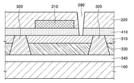
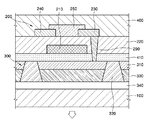
200 有機薄膜トランジスタ、
210 ゲート電極、
220 ゲート絶縁層、
230 ドレイン電極、
240 ソース電極、
250 有機半導体部、
290 層間接続部、
300 有機発光ダイオード、
310 ピクセル電極、
320 バンク部、
330 有機発光層、
340 透明電極、
410 平坦化膜。
Claims (2)
- 透明基板の上面に透明電極、有機発光層、及びピクセル電極を順次に積層して有機発光ダイオードを形成する段階と、
前記有機発光ダイオードを覆う平坦化膜を形成する段階と、
前記平坦化膜の上面にゲート電極を形成し、その上にゲート絶縁層を覆った後、前記有機発光ダイオードのピクセル電極に至るまで一側をエッチングしてビアホールを形成する段階と、
ソース電極及びドレイン電極を形成するが、前記ドレイン電極が前記ビアホールを通じて前記ピクセル電極と連結されるようにする段階と、
前記ソース電極とドレイン電極との間に、前記有機発光ダイオードを形成する段階の工程温度よりも低い工程温度で有機半導体部を形成する段階と、を含み、
前記有機発光ダイオードを形成する段階は、
前記基板の上面全体に透明電極層を形成する段階と、
前記透明電極層の上面に発光領域を区画するバンク部を形成する段階と、
前記バンク部の内部の前記透明電極層の上面に有機発光層を形成する段階と、
前記有機発光層の上面にピクセル電極を形成する段階と、を含むことを特徴とする底面発光型の有機発光素子の製造方法。 - 透明基板の上面に透明電極、有機発光層、及びピクセル電極を順次に積層して有機発光ダイオードを形成する段階と、
前記有機発光ダイオードを覆う平坦化膜を形成する段階と、
前記有機発光ダイオードのピクセル電極に至るまで平坦化膜の一側をエッチングしてビアホールを形成する段階と、
前記平坦化膜の上面にソース電極及びドレイン電極を形成するが、前記ドレイン電極が前記ビアホールを通じて前記ピクセル電極と連結されるようにする段階と、
前記ソース電極とドレイン電極との間に、前記有機発光ダイオードを形成する段階の工程温度よりも低い工程温度で有機半導体部を形成する段階と、
前記ソース電極、ドレイン電極、及び有機半導体部の上部にゲート絶縁膜を形成し、その上にゲート電極を形成する段階と、を含み、
前記有機発光ダイオードを形成する段階は、
前記基板の上面全体に透明電極層を形成する段階と、
前記透明電極層の上面に発光領域を区画するバンク部を形成する段階と、
前記バンク部の内部の前記透明電極層の上面に有機発光層を形成する段階と、
前記有機発光層の上面にピクセル電極を形成する段階と、を含むことを特徴とする底面発光型の有機発光素子の製造方法。
Applications Claiming Priority (2)
| Application Number | Priority Date | Filing Date | Title |
|---|---|---|---|
| KR1020050033199A KR100647325B1 (ko) | 2005-04-21 | 2005-04-21 | 저면발광형 유기발광소자 |
| KR10-2005-0033199 | 2005-04-21 |
Publications (3)
| Publication Number | Publication Date |
|---|---|
| JP2006303476A JP2006303476A (ja) | 2006-11-02 |
| JP2006303476A5 JP2006303476A5 (ja) | 2009-04-30 |
| JP5094032B2 true JP5094032B2 (ja) | 2012-12-12 |
Family
ID=37186153
Family Applications (1)
| Application Number | Title | Priority Date | Filing Date |
|---|---|---|---|
| JP2006081406A Active JP5094032B2 (ja) | 2005-04-21 | 2006-03-23 | 底面発光型の有機発光素子の製造方法 |
Country Status (3)
| Country | Link |
|---|---|
| US (1) | US7626331B2 (ja) |
| JP (1) | JP5094032B2 (ja) |
| KR (1) | KR100647325B1 (ja) |
Families Citing this family (16)
| Publication number | Priority date | Publication date | Assignee | Title |
|---|---|---|---|---|
| KR100741968B1 (ko) * | 2004-11-23 | 2007-07-23 | 삼성에스디아이 주식회사 | 유기 전계 발광 표시 소자 및 그 제조방법 |
| TWI364839B (en) * | 2006-11-17 | 2012-05-21 | Au Optronics Corp | Pixel structure of active matrix organic light emitting display and fabrication method thereof |
| KR100869646B1 (ko) * | 2007-07-27 | 2008-11-21 | 경북대학교 산학협력단 | 유기박막트랜지스터가 내장된 능동형유기전기발광디스플레이소자 및 이의 제조 방법 |
| KR20100007266A (ko) * | 2008-07-11 | 2010-01-22 | 삼성모바일디스플레이주식회사 | 유기 발광 표시 장치 및 그 제조 방법 |
| CN102804430B (zh) * | 2010-01-19 | 2015-11-25 | Lg伊诺特有限公司 | 封装结构及其制造方法 |
| WO2012173086A1 (ja) * | 2011-06-15 | 2012-12-20 | シャープ株式会社 | 半導体装置およびその製造方法 |
| KR101942515B1 (ko) * | 2012-05-03 | 2019-01-28 | 삼성디스플레이 주식회사 | 유기 발광 표시 장치 및 유기 발광 표시 장치 제조 방법 |
| KR101887942B1 (ko) | 2012-05-07 | 2018-08-14 | 삼성전자주식회사 | 발광소자 |
| GB2517489A (en) * | 2013-08-23 | 2015-02-25 | Plastic Logic Ltd | Planarisation Layers |
| KR102089248B1 (ko) * | 2013-09-23 | 2020-03-16 | 엘지디스플레이 주식회사 | 유기발광다이오드소자 및 그의 제조방법 |
| US9105615B1 (en) | 2014-06-12 | 2015-08-11 | Amazon Technologies, Inc. | Substrate vias for a display device |
| KR102319829B1 (ko) * | 2014-11-07 | 2021-11-01 | 엘지디스플레이 주식회사 | 유기 발광 표시 장치 |
| CN108538902B (zh) * | 2018-05-21 | 2020-09-01 | 深圳市华星光电技术有限公司 | Oled背板的制作方法及oled背板 |
| US11322542B2 (en) * | 2020-03-27 | 2022-05-03 | Harvatek Corporation | Light-emitting diode (LED) assembly and method of manufacturing an LED cell of the same |
| CN114255703B (zh) * | 2020-09-21 | 2023-06-16 | 京东方科技集团股份有限公司 | 显示基板及显示装置 |
| CN114447026A (zh) * | 2022-02-14 | 2022-05-06 | 成都捷翼电子科技有限公司 | 一种有机图像传感器制造方法 |
Family Cites Families (17)
| Publication number | Priority date | Publication date | Assignee | Title |
|---|---|---|---|---|
| JP4423767B2 (ja) * | 2000-08-22 | 2010-03-03 | ソニー株式会社 | 有機電界発光素子及びその製造方法 |
| JP2002083691A (ja) * | 2000-09-06 | 2002-03-22 | Sharp Corp | アクティブマトリックス駆動型有機led表示装置及びその製造方法 |
| JP2002215065A (ja) * | 2000-11-02 | 2002-07-31 | Seiko Epson Corp | 有機エレクトロルミネッセンス装置及びその製造方法、並びに電子機器 |
| TW533446B (en) * | 2000-12-22 | 2003-05-21 | Koninkl Philips Electronics Nv | Electroluminescent device and a method of manufacturing thereof |
| JP2003258267A (ja) * | 2002-03-05 | 2003-09-12 | Pioneer Electronic Corp | 有機薄膜半導体素子及びその製造方法 |
| TW546853B (en) * | 2002-05-01 | 2003-08-11 | Au Optronics Corp | Active type OLED and the fabrication method thereof |
| TW554525B (en) * | 2002-08-28 | 2003-09-21 | Ind Tech Res Inst | Organic integration device of thin film transistor and light emitting diode |
| TWI297553B (ja) * | 2002-08-28 | 2008-06-01 | Ind Tech Res Inst | |
| TWI228687B (en) * | 2003-01-22 | 2005-03-01 | Toppoly Optoelectronics Corp | Active-type organic electroluminescent display and fabrication method thereof |
| JP3865245B2 (ja) * | 2003-03-12 | 2007-01-10 | 富士電機ホールディングス株式会社 | 有機elディスプレイの製造方法および製造装置 |
| JP4534430B2 (ja) * | 2003-04-24 | 2010-09-01 | セイコーエプソン株式会社 | 電気光学装置、電気光学装置用基板、電気光学装置の製造方法および電子機器 |
| JP2005063892A (ja) * | 2003-08-19 | 2005-03-10 | Seiko Epson Corp | 有機エレクトロルミネッセンス装置、及び有機エレクトロルミネッセンスel装置の製造方法、並びに電子機器 |
| US7227306B2 (en) * | 2003-08-28 | 2007-06-05 | Samsung Sdi Co., Ltd. | Organic electroluminescence display having recessed electrode structure |
| JP5005164B2 (ja) * | 2004-03-03 | 2012-08-22 | 株式会社ジャパンディスプレイイースト | 発光素子,発光型表示装置及び照明装置 |
| KR100601370B1 (ko) * | 2004-04-28 | 2006-07-13 | 삼성에스디아이 주식회사 | 박막 트랜지스터 및 그를 이용한 유기 전계 발광 표시 장치 |
| KR100741968B1 (ko) * | 2004-11-23 | 2007-07-23 | 삼성에스디아이 주식회사 | 유기 전계 발광 표시 소자 및 그 제조방법 |
| JP2006243127A (ja) * | 2005-03-01 | 2006-09-14 | Victor Co Of Japan Ltd | シートディスプレイ |
-
2005
- 2005-04-21 KR KR1020050033199A patent/KR100647325B1/ko active IP Right Grant
-
2006
- 2006-03-23 JP JP2006081406A patent/JP5094032B2/ja active Active
- 2006-04-18 US US11/405,766 patent/US7626331B2/en active Active
Also Published As
| Publication number | Publication date |
|---|---|
| KR20060110701A (ko) | 2006-10-25 |
| JP2006303476A (ja) | 2006-11-02 |
| US20060238115A1 (en) | 2006-10-26 |
| US7626331B2 (en) | 2009-12-01 |
| KR100647325B1 (ko) | 2006-11-23 |
Similar Documents
| Publication | Publication Date | Title |
|---|---|---|
| JP5094032B2 (ja) | 底面発光型の有機発光素子の製造方法 | |
| US10312308B2 (en) | Organic light emitting device and method for manufacturing same | |
| JP5576210B2 (ja) | 有機発光ディスプレイ装置及びその製造方法 | |
| JP5969450B2 (ja) | 有機発光ディスプレイ装置および有機発光ディスプレイ装置の製造方法 | |
| KR101480973B1 (ko) | 유기 일렉트로루미네센스 표시 장치 | |
| KR102413938B1 (ko) | 발광 표시 장치 및 그 제조 방법 | |
| JP4732084B2 (ja) | 発光素子用の基板、その製造方法、発光素子用の電極、及びこれを備えた発光素子 | |
| JP4288918B2 (ja) | 有機elパネルおよびその製造方法、それを用いた電気光学パネル並びに電子機器 | |
| KR100646297B1 (ko) | 표시 장치의 제조 방법 | |
| JP2005327674A (ja) | 有機エレクトロルミネッセント表示素子、それを有する表示装置、及び、その製造方法 | |
| US9343514B2 (en) | Organic light emitting diode display and method of manufacturing the same | |
| JPWO2009113239A1 (ja) | 有機elディスプレイパネル及びその製造方法 | |
| JP2023503668A (ja) | ディスプレイパネル、フレキシブルディスプレイ、電子デバイスおよびディスプレイパネルの製造方法 | |
| KR20190080469A (ko) | 전계발광 표시 장치 | |
| US9917144B2 (en) | Display panel and method for manufacturing same | |
| US11245085B2 (en) | Self light-emitting element and manufacturing process of self light-emitting element, self light-emitting display device, and electronic equipment | |
| JP2006004743A (ja) | 表示装置及びその製造方法 | |
| JP6220208B2 (ja) | 有機エレクトロルミネッセンス表示装置及びその製造方法 | |
| JP2005284276A (ja) | 表示装置の製造方法 | |
| JP4900876B2 (ja) | 表示装置の製造方法 | |
| TWI262742B (en) | Method for manufacturing organic electroluminescence device and electronic apparatus | |
| JP7014421B2 (ja) | 有機el表示パネル及び有機el表示パネルの製造方法 | |
| JP2003217834A (ja) | 自己発光表示装置及びその製造方法 | |
| KR100709195B1 (ko) | 유기 발광 표시 장치 및 그 제조 방법 | |
| KR101994836B1 (ko) | 실리콘 산화물과 실리콘 질화물을 포함하는 배리어층을 구비한 tft 기판, 상기 tft 기판을 포함하는 유기 발광 표시 장치 및 상기 tft 기판의 제조 방법 |
Legal Events
| Date | Code | Title | Description |
|---|---|---|---|
| A521 | Request for written amendment filed |
Free format text: JAPANESE INTERMEDIATE CODE: A523 Effective date: 20090313 |
|
| A621 | Written request for application examination |
Free format text: JAPANESE INTERMEDIATE CODE: A621 Effective date: 20090313 |
|
| A131 | Notification of reasons for refusal |
Free format text: JAPANESE INTERMEDIATE CODE: A131 Effective date: 20110830 |
|
| A977 | Report on retrieval |
Free format text: JAPANESE INTERMEDIATE CODE: A971007 Effective date: 20110831 |
|
| A521 | Request for written amendment filed |
Free format text: JAPANESE INTERMEDIATE CODE: A523 Effective date: 20111129 |
|
| A02 | Decision of refusal |
Free format text: JAPANESE INTERMEDIATE CODE: A02 Effective date: 20111220 |
|
| A521 | Request for written amendment filed |
Free format text: JAPANESE INTERMEDIATE CODE: A523 Effective date: 20120420 |
|
| A911 | Transfer to examiner for re-examination before appeal (zenchi) |
Free format text: JAPANESE INTERMEDIATE CODE: A911 Effective date: 20120501 |
|
| TRDD | Decision of grant or rejection written | ||
| A01 | Written decision to grant a patent or to grant a registration (utility model) |
Free format text: JAPANESE INTERMEDIATE CODE: A01 Effective date: 20120828 |
|
| A01 | Written decision to grant a patent or to grant a registration (utility model) |
Free format text: JAPANESE INTERMEDIATE CODE: A01 |
|
| A61 | First payment of annual fees (during grant procedure) |
Free format text: JAPANESE INTERMEDIATE CODE: A61 Effective date: 20120918 |
|
| R150 | Certificate of patent or registration of utility model |
Ref document number: 5094032 Country of ref document: JP Free format text: JAPANESE INTERMEDIATE CODE: R150 Free format text: JAPANESE INTERMEDIATE CODE: R150 |
|
| FPAY | Renewal fee payment (event date is renewal date of database) |
Free format text: PAYMENT UNTIL: 20150928 Year of fee payment: 3 |
|
| FPAY | Renewal fee payment (event date is renewal date of database) |
Free format text: PAYMENT UNTIL: 20150928 Year of fee payment: 3 |
|
| S111 | Request for change of ownership or part of ownership |
Free format text: JAPANESE INTERMEDIATE CODE: R313111 |
|
| S631 | Written request for registration of reclamation of domicile |
Free format text: JAPANESE INTERMEDIATE CODE: R313631 |
|
| FPAY | Renewal fee payment (event date is renewal date of database) |
Free format text: PAYMENT UNTIL: 20150928 Year of fee payment: 3 |
|
| R371 | Transfer withdrawn |
Free format text: JAPANESE INTERMEDIATE CODE: R371 |
|
| S111 | Request for change of ownership or part of ownership |
Free format text: JAPANESE INTERMEDIATE CODE: R313111 |
|
| S631 | Written request for registration of reclamation of domicile |
Free format text: JAPANESE INTERMEDIATE CODE: R313631 |
|
| FPAY | Renewal fee payment (event date is renewal date of database) |
Free format text: PAYMENT UNTIL: 20150928 Year of fee payment: 3 |
|
| R350 | Written notification of registration of transfer |
Free format text: JAPANESE INTERMEDIATE CODE: R350 |
|
| R250 | Receipt of annual fees |
Free format text: JAPANESE INTERMEDIATE CODE: R250 |
|
| R250 | Receipt of annual fees |
Free format text: JAPANESE INTERMEDIATE CODE: R250 |
|
| R250 | Receipt of annual fees |
Free format text: JAPANESE INTERMEDIATE CODE: R250 |
|
| R250 | Receipt of annual fees |
Free format text: JAPANESE INTERMEDIATE CODE: R250 |
|
| R250 | Receipt of annual fees |
Free format text: JAPANESE INTERMEDIATE CODE: R250 |
|
| R250 | Receipt of annual fees |
Free format text: JAPANESE INTERMEDIATE CODE: R250 |
|
| R250 | Receipt of annual fees |
Free format text: JAPANESE INTERMEDIATE CODE: R250 |
|
| R250 | Receipt of annual fees |
Free format text: JAPANESE INTERMEDIATE CODE: R250 |
|
| R250 | Receipt of annual fees |
Free format text: JAPANESE INTERMEDIATE CODE: R250 |
|
| R250 | Receipt of annual fees |
Free format text: JAPANESE INTERMEDIATE CODE: R250 |