JP5094032B2 - Manufacturing method of bottom-emitting organic light-emitting device - Google Patents
Manufacturing method of bottom-emitting organic light-emitting device Download PDFInfo
- Publication number
- JP5094032B2 JP5094032B2 JP2006081406A JP2006081406A JP5094032B2 JP 5094032 B2 JP5094032 B2 JP 5094032B2 JP 2006081406 A JP2006081406 A JP 2006081406A JP 2006081406 A JP2006081406 A JP 2006081406A JP 5094032 B2 JP5094032 B2 JP 5094032B2
- Authority
- JP
- Japan
- Prior art keywords
- light emitting
- organic light
- forming
- electrode
- layer
- Prior art date
- Legal status (The legal status is an assumption and is not a legal conclusion. Google has not performed a legal analysis and makes no representation as to the accuracy of the status listed.)
- Active
Links
- 238000004519 manufacturing process Methods 0.000 title claims description 20
- 238000000034 method Methods 0.000 claims description 56
- 239000000758 substrate Substances 0.000 claims description 25
- 239000004065 semiconductor Substances 0.000 claims description 11
- 238000005530 etching Methods 0.000 claims description 6
- 238000010030 laminating Methods 0.000 claims 2
- 238000000638 solvent extraction Methods 0.000 claims 2
- 239000010410 layer Substances 0.000 description 36
- 239000010408 film Substances 0.000 description 23
- 239000011159 matrix material Substances 0.000 description 10
- 239000010409 thin film Substances 0.000 description 9
- QVGXLLKOCUKJST-UHFFFAOYSA-N atomic oxygen Chemical compound [O] QVGXLLKOCUKJST-UHFFFAOYSA-N 0.000 description 7
- 229910052760 oxygen Inorganic materials 0.000 description 7
- 239000001301 oxygen Substances 0.000 description 7
- 238000010586 diagram Methods 0.000 description 6
- 238000007641 inkjet printing Methods 0.000 description 6
- 239000000463 material Substances 0.000 description 5
- 238000000059 patterning Methods 0.000 description 5
- 230000001681 protective effect Effects 0.000 description 5
- 239000011229 interlayer Substances 0.000 description 4
- 239000002184 metal Substances 0.000 description 4
- XLYOFNOQVPJJNP-UHFFFAOYSA-N water Substances O XLYOFNOQVPJJNP-UHFFFAOYSA-N 0.000 description 4
- 230000015572 biosynthetic process Effects 0.000 description 3
- 230000006866 deterioration Effects 0.000 description 3
- 238000005192 partition Methods 0.000 description 3
- 239000002356 single layer Substances 0.000 description 3
- 239000003990 capacitor Substances 0.000 description 2
- 238000009413 insulation Methods 0.000 description 2
- 239000011368 organic material Substances 0.000 description 2
- 238000000206 photolithography Methods 0.000 description 2
- 238000003860 storage Methods 0.000 description 2
- 238000004381 surface treatment Methods 0.000 description 2
- 230000004888 barrier function Effects 0.000 description 1
- 230000004397 blinking Effects 0.000 description 1
- 230000015556 catabolic process Effects 0.000 description 1
- 239000004020 conductor Substances 0.000 description 1
- 238000006731 degradation reaction Methods 0.000 description 1
- 238000000151 deposition Methods 0.000 description 1
- 230000008021 deposition Effects 0.000 description 1
- 238000001312 dry etching Methods 0.000 description 1
- 238000005401 electroluminescence Methods 0.000 description 1
- 239000011521 glass Substances 0.000 description 1
- AMGQUBHHOARCQH-UHFFFAOYSA-N indium;oxotin Chemical compound [In].[Sn]=O AMGQUBHHOARCQH-UHFFFAOYSA-N 0.000 description 1
- 238000002347 injection Methods 0.000 description 1
- 239000007924 injection Substances 0.000 description 1
- 239000011810 insulating material Substances 0.000 description 1
- 238000003475 lamination Methods 0.000 description 1
- 238000012986 modification Methods 0.000 description 1
- 230000004048 modification Effects 0.000 description 1
- 239000012044 organic layer Substances 0.000 description 1
- 230000035484 reaction time Effects 0.000 description 1
- 238000004528 spin coating Methods 0.000 description 1
- 238000004544 sputter deposition Methods 0.000 description 1
- 238000001771 vacuum deposition Methods 0.000 description 1
- 238000001039 wet etching Methods 0.000 description 1
Images


Classifications
-
- H—ELECTRICITY
- H10—SEMICONDUCTOR DEVICES; ELECTRIC SOLID-STATE DEVICES NOT OTHERWISE PROVIDED FOR
- H10K—ORGANIC ELECTRIC SOLID-STATE DEVICES
- H10K10/00—Organic devices specially adapted for rectifying, amplifying, oscillating or switching; Organic capacitors or resistors having a potential-jump barrier or a surface barrier
- H10K10/80—Constructional details
-
- H—ELECTRICITY
- H05—ELECTRIC TECHNIQUES NOT OTHERWISE PROVIDED FOR
- H05B—ELECTRIC HEATING; ELECTRIC LIGHT SOURCES NOT OTHERWISE PROVIDED FOR; CIRCUIT ARRANGEMENTS FOR ELECTRIC LIGHT SOURCES, IN GENERAL
- H05B33/00—Electroluminescent light sources
- H05B33/12—Light sources with substantially two-dimensional radiating surfaces
- H05B33/22—Light sources with substantially two-dimensional radiating surfaces characterised by the chemical or physical composition or the arrangement of auxiliary dielectric or reflective layers
-
- H—ELECTRICITY
- H05—ELECTRIC TECHNIQUES NOT OTHERWISE PROVIDED FOR
- H05B—ELECTRIC HEATING; ELECTRIC LIGHT SOURCES NOT OTHERWISE PROVIDED FOR; CIRCUIT ARRANGEMENTS FOR ELECTRIC LIGHT SOURCES, IN GENERAL
- H05B33/00—Electroluminescent light sources
- H05B33/10—Apparatus or processes specially adapted to the manufacture of electroluminescent light sources
-
- H—ELECTRICITY
- H10—SEMICONDUCTOR DEVICES; ELECTRIC SOLID-STATE DEVICES NOT OTHERWISE PROVIDED FOR
- H10K—ORGANIC ELECTRIC SOLID-STATE DEVICES
- H10K10/00—Organic devices specially adapted for rectifying, amplifying, oscillating or switching; Organic capacitors or resistors having a potential-jump barrier or a surface barrier
- H10K10/40—Organic transistors
- H10K10/46—Field-effect transistors, e.g. organic thin-film transistors [OTFT]
- H10K10/462—Insulated gate field-effect transistors [IGFETs]
- H10K10/466—Lateral bottom-gate IGFETs comprising only a single gate
-
- H—ELECTRICITY
- H10—SEMICONDUCTOR DEVICES; ELECTRIC SOLID-STATE DEVICES NOT OTHERWISE PROVIDED FOR
- H10K—ORGANIC ELECTRIC SOLID-STATE DEVICES
- H10K50/00—Organic light-emitting devices
- H10K50/80—Constructional details
- H10K50/84—Passivation; Containers; Encapsulations
- H10K50/844—Encapsulations
Description
本発明は、有機発光ダイオード(OLED)を用いた有機発光素子の製造方法に係り、さらに詳細には、ピクセルごとに有機薄膜トランジスタを用いて、前記有機発光ダイオードを駆動するピクセル回路を備えるアクティブマトリックス駆動方式の底面発光型の有機発光素子の製造方法に関する。 The present invention relates to a method of manufacturing an organic light emitting device using an organic light emitting diode (OLED), and more particularly, an active matrix driving including an organic thin film transistor for each pixel and a pixel circuit for driving the organic light emitting diode. The present invention relates to a method of manufacturing a bottom-emitting organic light-emitting element of the type .
一般に、有機発光ダイオード(OLED:Organic Light Emitting Diode)とは、低分子または高分子の有機物薄膜で負極と正極とを通じて注入された電子と正孔とが再結合して励起子を形成し、形成された励起子のエネルギーにより特定波長の光が発生する、いわゆる有機電界発光現象を用いた発光素子を言う。 In general, an organic light emitting diode (OLED) is a low molecular or high molecular organic thin film that recombines electrons and holes injected through a negative electrode and a positive electrode to form excitons. A light-emitting element using a so-called organic electroluminescence phenomenon in which light of a specific wavelength is generated by the energy of excitons.
このような有機発光ダイオードを用いた表示装置は、その駆動方式によってパッシブマトリックス型とアクティブマトリックス型とに分けられる。この中、アクティブマトリックス型の有機発光素子は、マトリックス形態に配列されたピクセルごとにそれを駆動するピクセル回路を備える。前記ピクセル回路は、薄膜トランジスタ(TFT:Thin−Film Transister)によりスイッチングされ、ピクセル関連情報を保存する。このようなアクティブマトリックス型は、パッシブマトリックス型に比べて有機発光ダイオードをさらに速い速度で駆動できるため、対比特性が優秀であり、画面の明滅も少なく、反応時間特性も優れるという長所を有する。 Display devices using such organic light emitting diodes are classified into a passive matrix type and an active matrix type depending on the driving method. Among these, the active matrix organic light emitting device includes a pixel circuit that drives each pixel arranged in a matrix form. The pixel circuit is switched by a thin film transistor (TFT) and stores pixel related information. Such an active matrix type has advantages in that the organic light emitting diode can be driven at a higher speed than the passive matrix type, and thus has excellent contrast characteristics, less screen blinking, and excellent reaction time characteristics.
図1は、従来のアクティブマトリックス型の有機発光素子の例を概略的に示した断面図である。構造を理解しやすくするために、スイッチングTFTとOLEDとを備える単位ピクセルの断面を示した。前記の例によると、基板10の上面の一側にはTFT20構造が備えられ、他側には、OLED30構造が備えられている。特許文献1に開示された有機発光素子などがこれに属するものであって、前記TFT20構造は、ゲート電極21、ゲート絶縁層22、ソース電極24、ドレイン電極23、及び半導体部25を有し、前記OLED30構造は、前記ドレイン電極23と連結されたピクセル電極31、発光領域を区画するバンク部32、前記発光領域内に順次に積層された有機発光層33、及び透明電極34を有する。
FIG. 1 is a cross-sectional view schematically showing an example of a conventional active matrix organic light emitting device. In order to facilitate understanding of the structure, a cross section of a unit pixel including a switching TFT and an OLED is shown. According to the above example, the
前記の例による有機発光素子は、構造が単純で、かつ製造が容易な反面、単位ピクセル面積に対する前記発光領域が占める面積の比、すなわち開口率が低いという短所がある。 The organic light emitting device according to the above example has a simple structure and is easy to manufacture, but has a disadvantage that a ratio of an area occupied by the light emitting region to a unit pixel area, that is, an aperture ratio is low.
図2は、従来の上面発光型の有機発光素子の例を概略的に示した断面図である。前記図1と同様に、構造を理解しやすくするために、スイッチングTFTとOLEDとを備える単位ピクセルの断面を示した。第2例によると、基板10上に薄膜トランジスタ20構造が備えられ、その上の重畳される領域に有機発光ダイオード30構造が備えられている。特許文献2に開示された有機発光素子などがこれに属するものであって、前記TFT20構造と前記OLED30との間には平坦化膜41が備えられ、前記TFT20のドレイン電極23は、層間接続部29を通じて前記OLED30のピクセル電極31と連結される。
FIG. 2 is a cross-sectional view schematically showing an example of a conventional top emission type organic light emitting device. As in FIG. 1, a cross section of a unit pixel including a switching TFT and an OLED is shown for easy understanding of the structure. According to the second example, the
前記例による有機発光素子は、構造的にピクセルの大部分を発光領域として使用できて開口率が高い反面、OLED30が外気と近く配置されるので、水、水蒸気及び酸素との接触に脆弱であるという短所がある。 The organic light emitting device according to the above example can structurally use most of the pixels as a light emitting region and has a high aperture ratio. However, since the OLED 30 is arranged close to the outside air, it is vulnerable to contact with water, water vapor and oxygen. There are disadvantages.
また、前記上面発光型の有機発光表示装置において、TFT20構造として有機薄膜トランジスタ(OTFT)を使用する場合、通常的にOLED30の工程温度がOTFT工程温度より高いため、OLED30の工程時に既に形成されたOTFTの劣化をもたらすおそれがあるという問題がある。
本発明は、基板の上面に有機発光ダイオードを備え、その上に少なくとも一部が重畳されて配置された有機薄膜トランジスタを備えるピクセル回路を備えることによって、高い開口率を有すると同時に外気による有機発光ダイオードの劣化を減少させる構造を有する底面発光型の有機発光素子の製造方法を提供するところにその目的がある。 The present invention includes an organic light emitting diode provided on an upper surface of a substrate, and a pixel circuit including an organic thin film transistor disposed at least partially on the organic light emitting diode. An object of the present invention is to provide a method of manufacturing a bottom-emitting organic light-emitting device having a structure that reduces deterioration of the substrate.
また、本発明は、相対的に高い工程温度を伴う有機発光ダイオードを基板上に先に形成し、その上に相対的に低い工程温度を伴う有機薄膜トランジスタを形成することによって、製造工程において発生するディバイスの劣化を防止できる構造の底面発光型の有機発光素子の製造方法を提供するところにその目的がある。 In addition, the present invention occurs in a manufacturing process by first forming an organic light emitting diode with a relatively high process temperature on a substrate and forming an organic thin film transistor with a relatively low process temperature thereon. The object is to provide a method of manufacturing a bottom-emitting organic light-emitting device having a structure capable of preventing device deterioration.
本発明による底面発光型の有機発光素子の製造方法は、透明基板の上面に透明電極、有機発光層、及びピクセル電極を順次に積層して有機発光ダイオードを形成する段階と、前記有機発光ダイオードを覆う平坦化膜を形成する段階と、前記平坦化膜の上面にゲート電極を形成し、その上にゲート絶縁層を覆った後、前記有機発光ダイオードのピクセル電極に至るまで一側をエッチングしてビアホールを形成する段階と、ソース電極及びドレイン電極を形成するが、前記ドレイン電極が前記ビアホールを通じて前記ピクセル電極と連結されるようにする段階と、前記ソース電極とドレイン電極との間に、前記有機発光ダイオードを形成する段階の工程温度よりも低い工程温度で有機半導体部を形成する段階と、を含み、前記有機発光ダイオードを形成する段階は、前記基板の上面全体に透明電極層を形成する段階と、前記透明電極層の上面に発光領域を区画するバンク部を形成する段階と、前記バンク部の内部の前記透明電極層の上面に有機発光層を形成する段階と、前記有機発光層の上面にピクセル電極を形成する段階と、を含むことを特徴とする。 A method of manufacturing a bottom-emitting organic light emitting device according to the present invention includes a step of sequentially forming a transparent electrode, an organic light emitting layer, and a pixel electrode on an upper surface of a transparent substrate to form an organic light emitting diode; Forming a covering planarizing film; and forming a gate electrode on the upper surface of the planarizing film, covering the gate insulating layer thereon, and then etching one side until reaching the pixel electrode of the organic light emitting diode Forming a via hole; forming a source electrode and a drain electrode, wherein the drain electrode is connected to the pixel electrode through the via hole; and the organic layer between the source electrode and the drain electrode. wherein forming the organic semiconductor portion at a lower process temperature than the process temperature of the step of forming a light-emitting diode, wherein the organic light emitting diode Forming a transparent electrode layer on the entire upper surface of the substrate; forming a bank portion defining a light emitting region on the upper surface of the transparent electrode layer; and the transparent electrode layer inside the bank portion. Forming an organic light emitting layer on the upper surface of the organic light emitting layer, and forming a pixel electrode on the upper surface of the organic light emitting layer.
本発明による底面発光型の有機発光素子の製造方法は、高い開口率を有すると同時に、水、水蒸気及び酸素に対して相対的に強いOTFTがOLEDを保護する障壁の役割を果たす底面発光型の有機発光素子が形成でき、また、工程温度の側面で工程の安定性を向上させることができる。 The method for manufacturing a bottom emission type organic light emitting device according to the present invention has a high aperture ratio, and at the same time, an OTFT relatively strong against water, water vapor and oxygen serves as a barrier to protect the OLED. An organic light-emitting element can be formed, and process stability can be improved in terms of process temperature .
以下、添付した図面を参照して、本発明の実施形態を通じて本発明の特徴及び長所を詳細に説明する。同じ図面符号は、同じ部材または部分を意味する。 Hereinafter, the features and advantages of the present invention will be described in detail through embodiments of the present invention with reference to the accompanying drawings. The same reference numerals refer to the same members or parts.
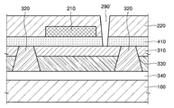
図3は、本発明による底面発光型の有機発光素子の実施形態を概略的に示した断面図である。構造を理解しやすくするために、スイッチングOTFTとOLEDとを備える単位ピクセルの断面を示した。 FIG. 3 is a cross-sectional view schematically illustrating an embodiment of a bottom emission organic light emitting device according to the present invention. In order to facilitate understanding of the structure, a cross section of a unit pixel including a switching OTFT and an OLED is shown.
本実施形態による有機発光素子は、透明基板100と、前記透明基板100の上面に備えられたOLED300構造及びこれを覆う平坦化面上に備えられたOTFT200構造を有し、前記透明基板100側に発光されることを特徴とする。前記透明基板100は、透明なガラス基板またはプラスチック基板でありうる。
The organic light emitting device according to the present embodiment has a
前記透明基板100の上側には、下向発光のOLED300構造が備えられる。すなわち、前記基板100の上面に透明電極340が備えられ、その上に隔膜形態で設置されてピクセルの発光領域を区画するバンク部320が備えられる。前記バンク部320内側の発光領域には、有機発光層330及びピクセル電極310が積層された形態で備えられる。ここで、前記透明電極340は、透光性と導電性とを同時に有するものであって、例えば、ITO(Indume−Tin Oxide)により形成されることが望ましい。また、前記透明電極340は、前記基板100の上面全体にわたって形成された共通電極でありうる。前記ピクセル電極310は、前記有機発光層330から発光する光に対して反射率の高い金属電極であることが望ましい。
A downwardly emitting
前記有機発光層330は、少なくとも一つの発光層(EML:Emitting Layer)を備えるものであって、単層構造に限定されずに、相互対向する両電極間に電子輸送層(ETL)、正孔輸送層(HTL)、正孔注入層(HIL)などを選択的にさらに備えて有機発光効率を増大させた多層構造を含む概念である。例えば、前記有機発光層330がETL、EML及びHTLの積層構造からなる場合(図示せず)、負極である前記透明電極340とEMLとの間にETLを備え、正極である前記ピクセル電極310と前記EMLとの間にHTLを備えることができる。ここで、EMLをはじめとして他の層は、既知の材料のうちどれでも形成可能であり、したがって、材料の選択によって本発明の技術的範囲が限定されない。
The organic
前記OLED300構造は、絶縁性の平坦化膜410で覆われており、前記平坦化膜410上には、OTFT200構造が備えられる。前記OTFT200構造は、ゲート電極210、ゲート絶縁層220、ソース電極240、ドレイン電極230、及び有機半導体部250を有し、従来の一般的なOTFT構造でありうる。ただし、前記平坦化膜410及びゲート絶縁層220の一側には、これらを貫通して前記OTFT200のドレイン電極230と前記OLED300のピクセル電極310とを電気的に連結する層間接続部290が備えられる。
The OLED 300 structure is covered with an
前記OTFT200構造は、その全部または一部が前記OLED300構造の発光領域に平面的に重畳されて備えられる。したがって、本実施形態による有機発光素子は、前記バンク部320を除外した全体面が発光領域として非常に高い開口率を有することができる。
The
また、本実施形態による有機発光素子は、その上面、すなわち前記OTFT200構造の上面に保護膜400を備えることができる。これは、外気に含まれた水分及び酸素から有機材料を保護する役割を果たす。
In addition, the organic light emitting device according to the present embodiment may include the
本発明によるOLED構造は、基板100側に有機発光層330が形成され、上部保護膜側に有機発光層330に比べて相対的に水分及び酸素に強い有機半導体部250が形成されることによって、従来の上面発光型OLED構造に対して水分と酸素によるディバイス劣化問題を減少させうるという長所がある。
In the OLED structure according to the present invention, the organic
以上の前記OLED300構造の上部には、前記OTFT200構造を含むピクセル回路が設置されて前記OLED300を駆動する。ピクセル回路は、一般的に前記ドライブOTFTだけでなく、スイッチングOTFT及びストレージキャパシタ構造などの、他の要素とそれらを連結するラインパターンとを備えて構成される。
A pixel circuit including the
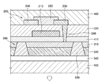
図4Aないし図4Eは、本発明による有機発光素子を製造する各工程を示した工程図である。 4A to 4E are process diagrams illustrating processes for manufacturing an organic light emitting device according to the present invention.
まず、図4Aに示したように、透明基板100を設け、その上面に透明電極340を形成する。ITOを真空蒸着またはスパッタリングして形成することが一般的であるが、素材や積層方法に関する特別な制限はない。この時、前記透明基板100の上面全体に対して一定の厚さに蒸着することが望ましい。透明電極340は、このようにITO単層膜より形成できるだけでなく、仕事関数に合うように非常に薄い金属膜と共に多層膜で形成されることもある。
First, as shown in FIG. 4A, a
次に、図4Bに示したように、単位ピクセル領域の縁部に垂直隔膜形態でバンク部320を形成してOLEDの発光領域を区画した後、その内側に有機発光層330及びピクセル電極310を順次に形成する。有機発光層330は、前記のように、少なくとも一つの発光層(EML)を有する単層または多層構造により形成され、その形成方法は、既知の方法によることができる。例えば、前記透明電極340の表面をプラズマ表面処理した後、インクジェットプリント法を用いて有機発光層330材料を塗布し、炉内または熱板上でキュアリングして形成できる。ピクセル電極310は、一例として、金属インクをインクジェットプリント法により塗布し、キュアリングして形成できる。これにより、透明基板100上に下向発光の有機発光ダイオード、すなわち、OLED構造が完成する。
Next, as shown in FIG. 4B, a
次に、前記OLED構造上に平坦化膜410を形成する。平坦化膜は、有機絶縁材料をスピンコーティング法で形成されうる。平坦化膜410で上面を平坦にした後、その上に少なくとも一つのOTFTを備えるピクセル回路を形成する。一般的に、アクティブマトリックス型の有機発光素子のピクセル回路には、スイッチングOTFT、ドライブOTFT、ストレージキャパシタ、及びこれらを連結するラインパターンなどを備えるが、キャパシタやラインパターンなどを形成する過程は、OTFTのゲート、ソース及びドレイン電極を形成する過程と同時に行うことができるので、ここでは、OTFT構造の形成過程を中心に説明する。
Next, a
図4Cに示したように、前記平坦化膜410上にゲート電極210を形成し、ゲート絶縁層220を覆った後、前記ゲート絶縁層220と平坦化膜410の一側を貫通して前記ピクセル電極310まで至るビアホール290’を形成する。一例として、エッチング法によりビアホール290’を形成する場合、前記ゲート絶縁層220の上面にレジスト膜を形成し、フォトリソグラフィ法でビアホールが形成される領域をパターニングした後、乾式エッチングあるいは湿式エッチングを用いてエッチングし、前記レジスト膜を除去する。また、レーザービームを用いて所望の位置のゲート絶縁膜を除去する方法でビアホールを形成することもできる。
Referring to FIG. 4C, a
次に、図4Dに示したように、OTFT構造のソース電極240とドレイン電極230とを形成する。この時、ドレイン電極230の形成と同時に、または先行して前記ビアホール290’を導電性材料で充填することによって、層間接続部290を形成する。ソース、ドレイン電極240、230のパターニング方法としては、金属インクを用いるインクジェットプリント法が望ましい。また、前記電極のパターニングに先立って前記ゲート絶縁層220上に表面制御層を形成し、表面エネルギーパターニングする過程をさらに含みうる。次に、前記ソース電極240とドレイン電極230との間には、有機半導体部250を形成する。この過程もやはりプラズマ表面処理後にインクジェットプリント法により行うことができる。インクジェットプリント法によるパターニング後には、キュアリング過程が伴われる。
Next, as shown in FIG. 4D, a
前記有機半導体部250のキュアリング工程の温度は、先行工程であるOLED構造の形成過程中、有機発光層330のキュアリング工程の温度より低いことが望ましい。キュアリング工程の温度は、塗布された有機物質の種類によって可変的であるが、一般的に有機半導体物質が相対的に低温でキュアリングできるので、先行工程を通じてあらかじめ完成したOLED構造が変形または変質することを防止できる。
The temperature of the curing process of the
前述した製造方法において、電極などのパターニング過程は、インクジェットプリント法を用いると説明したが、これは、相対的に精度の低い大面積表示装置の製造に有利な方法であり、高い精密度が要求される小型、高解像度の表示装置の製造時には、フォトリソグラフィ法を含むエッチング工程によるのが有利であり得る。 In the above-described manufacturing method, it has been described that the ink-jet printing method is used for the patterning process of electrodes and the like, but this is an advantageous method for manufacturing a large area display device with relatively low accuracy, and high precision is required. When manufacturing a small-sized, high-resolution display device, it may be advantageous to use an etching process including a photolithography method.
完成したOTFT構造上には、保護膜400を形成して外気に含まれた水分、酸素などから表示装置の内部構造を保護することができる。ただし、OTFT構造は、OLEDに比べて水分及び酸素に強いので、前記保護膜400は、OLED構造が上部に配置された従来の表示装置(図2参照)の保護膜40に比べてさらに薄く形成できる。
A
以上で使われた有機発光素子という用語は、有機発光ダイオード(OLED)と有機薄膜トランジスタ(OTFT)とを備えて前記OLEDを駆動する駆動回路を備えるあらゆる装置を指すものである。 The term organic light emitting device used above refers to any device that includes an organic light emitting diode (OLED) and an organic thin film transistor (OTFT) and includes a drive circuit that drives the OLED.
以上、本発明による望ましい実施形態が説明されたが、これは、例示的なものに過ぎず、当業者ならば、これから多様な変形及び均等な他の実施形態が可能であるという点が理解できるであろう。したがって、本発明の技術的な保護範囲は、特許請求の範囲によって決定されなければならない。 Although the preferred embodiments according to the present invention have been described above, this is merely an example, and those skilled in the art can understand that various modifications and other equivalent embodiments are possible. Will. Therefore, the technical protection scope of the present invention must be determined by the claims.
本発明は、有機発光ダイオードを用いた有機発光素子の関連技術分野に好適に用いられる。 The present invention is suitably used in the related technical field of organic light emitting devices using organic light emitting diodes.
100 透明基板、
200 有機薄膜トランジスタ、
210 ゲート電極、
220 ゲート絶縁層、
230 ドレイン電極、
240 ソース電極、
250 有機半導体部、
290 層間接続部、
300 有機発光ダイオード、
310 ピクセル電極、
320 バンク部、
330 有機発光層、
340 透明電極、
410 平坦化膜。
100 transparent substrate,
200 organic thin film transistor,
210 gate electrode,
220 gate insulating layer,
230 drain electrode,
240 source electrode,
250 Organic Semiconductor Department,
290 interlayer connection,
300 organic light emitting diode,
310 pixel electrodes,
320 banks,
330 organic light emitting layer,
340 transparent electrode,
410 Planarization film.
Claims (2)
前記有機発光ダイオードを覆う平坦化膜を形成する段階と、
前記平坦化膜の上面にゲート電極を形成し、その上にゲート絶縁層を覆った後、前記有機発光ダイオードのピクセル電極に至るまで一側をエッチングしてビアホールを形成する段階と、
ソース電極及びドレイン電極を形成するが、前記ドレイン電極が前記ビアホールを通じて前記ピクセル電極と連結されるようにする段階と、
前記ソース電極とドレイン電極との間に、前記有機発光ダイオードを形成する段階の工程温度よりも低い工程温度で有機半導体部を形成する段階と、を含み、
前記有機発光ダイオードを形成する段階は、
前記基板の上面全体に透明電極層を形成する段階と、
前記透明電極層の上面に発光領域を区画するバンク部を形成する段階と、
前記バンク部の内部の前記透明電極層の上面に有機発光層を形成する段階と、
前記有機発光層の上面にピクセル電極を形成する段階と、を含むことを特徴とする底面発光型の有機発光素子の製造方法。 Forming an organic light emitting diode by sequentially laminating a transparent electrode, an organic light emitting layer, and a pixel electrode on the upper surface of the transparent substrate;
Forming a planarization film covering the organic light emitting diode;
Forming a gate electrode on the upper surface of the planarization film, covering a gate insulating layer thereon, etching one side until reaching a pixel electrode of the organic light emitting diode, and forming a via hole;
Forming a source electrode and a drain electrode, wherein the drain electrode is connected to the pixel electrode through the via hole;
Forming an organic semiconductor part at a process temperature lower than a process temperature of forming the organic light emitting diode between the source electrode and the drain electrode,
Forming the organic light emitting diode comprises:
Forming a transparent electrode layer over the entire top surface of the substrate;
Forming a bank portion for partitioning a light emitting region on the upper surface of the transparent electrode layer;
Forming an organic light emitting layer on the top surface of the transparent electrode layer inside the bank portion;
Forming a pixel electrode on the upper surface of the organic light emitting layer, and a method of manufacturing a bottom emission type organic light emitting device.
前記有機発光ダイオードを覆う平坦化膜を形成する段階と、
前記有機発光ダイオードのピクセル電極に至るまで平坦化膜の一側をエッチングしてビアホールを形成する段階と、
前記平坦化膜の上面にソース電極及びドレイン電極を形成するが、前記ドレイン電極が前記ビアホールを通じて前記ピクセル電極と連結されるようにする段階と、
前記ソース電極とドレイン電極との間に、前記有機発光ダイオードを形成する段階の工程温度よりも低い工程温度で有機半導体部を形成する段階と、
前記ソース電極、ドレイン電極、及び有機半導体部の上部にゲート絶縁膜を形成し、その上にゲート電極を形成する段階と、を含み、
前記有機発光ダイオードを形成する段階は、
前記基板の上面全体に透明電極層を形成する段階と、
前記透明電極層の上面に発光領域を区画するバンク部を形成する段階と、
前記バンク部の内部の前記透明電極層の上面に有機発光層を形成する段階と、
前記有機発光層の上面にピクセル電極を形成する段階と、を含むことを特徴とする底面発光型の有機発光素子の製造方法。 Forming an organic light emitting diode by sequentially laminating a transparent electrode, an organic light emitting layer, and a pixel electrode on the upper surface of the transparent substrate;
Forming a planarization film covering the organic light emitting diode;
Etching one side of the planarization film to the pixel electrode of the organic light emitting diode to form a via hole;
Forming a source electrode and a drain electrode on an upper surface of the planarization layer, the drain electrode being connected to the pixel electrode through the via hole;
Forming an organic semiconductor portion at a process temperature lower than a process temperature of forming the organic light emitting diode between the source electrode and the drain electrode;
Forming a gate insulating film on the source electrode, the drain electrode, and the organic semiconductor portion, and forming a gate electrode thereon,
Forming the organic light emitting diode comprises:
Forming a transparent electrode layer over the entire top surface of the substrate;
Forming a bank portion for partitioning a light emitting region on the upper surface of the transparent electrode layer;
Forming an organic light emitting layer on the top surface of the transparent electrode layer inside the bank portion;
Forming a pixel electrode on the upper surface of the organic light emitting layer, and a method of manufacturing a bottom emission type organic light emitting device.
Applications Claiming Priority (2)
| Application Number | Priority Date | Filing Date | Title |
|---|---|---|---|
| KR1020050033199A KR100647325B1 (en) | 2005-04-21 | 2005-04-21 | Organic light-emitting device of active matrix drive type and manufacturing method thereof |
| KR10-2005-0033199 | 2005-04-21 |
Publications (3)
| Publication Number | Publication Date |
|---|---|
| JP2006303476A JP2006303476A (en) | 2006-11-02 |
| JP2006303476A5 JP2006303476A5 (en) | 2009-04-30 |
| JP5094032B2 true JP5094032B2 (en) | 2012-12-12 |
Family
ID=37186153
Family Applications (1)
| Application Number | Title | Priority Date | Filing Date |
|---|---|---|---|
| JP2006081406A Active JP5094032B2 (en) | 2005-04-21 | 2006-03-23 | Manufacturing method of bottom-emitting organic light-emitting device |
Country Status (3)
| Country | Link |
|---|---|
| US (1) | US7626331B2 (en) |
| JP (1) | JP5094032B2 (en) |
| KR (1) | KR100647325B1 (en) |
Families Citing this family (15)
| Publication number | Priority date | Publication date | Assignee | Title |
|---|---|---|---|---|
| KR100741968B1 (en) * | 2004-11-23 | 2007-07-23 | 삼성에스디아이 주식회사 | Organic light emitting display device and fabricating method of the same |
| TWI364839B (en) * | 2006-11-17 | 2012-05-21 | Au Optronics Corp | Pixel structure of active matrix organic light emitting display and fabrication method thereof |
| KR100869646B1 (en) * | 2007-07-27 | 2008-11-21 | 경북대학교 산학협력단 | Active matrix organic light-emitting displays having organic thin film transistors and method of the same |
| KR20100007266A (en) * | 2008-07-11 | 2010-01-22 | 삼성모바일디스플레이주식회사 | Organic light emitting display apparatus and method of manufacturing thereof |
| WO2011090269A2 (en) * | 2010-01-19 | 2011-07-28 | Lg Innotek Co., Ltd. | Package and manufacturing method of the same |
| US20140124785A1 (en) * | 2011-06-15 | 2014-05-08 | Sharp Kabushiki Kaisha | Semiconductor device and method for manufacturing same |
| KR101942515B1 (en) * | 2012-05-03 | 2019-01-28 | 삼성디스플레이 주식회사 | Organic light emitting display apparatus and method of manufacturing the same |
| KR101887942B1 (en) * | 2012-05-07 | 2018-08-14 | 삼성전자주식회사 | Light emitting device |
| GB2517489A (en) * | 2013-08-23 | 2015-02-25 | Plastic Logic Ltd | Planarisation Layers |
| KR102089248B1 (en) * | 2013-09-23 | 2020-03-16 | 엘지디스플레이 주식회사 | Organic Light Emitting Diode Device And Method Of Fabricating The Same |
| US9105615B1 (en) * | 2014-06-12 | 2015-08-11 | Amazon Technologies, Inc. | Substrate vias for a display device |
| KR102319829B1 (en) * | 2014-11-07 | 2021-11-01 | 엘지디스플레이 주식회사 | Organic light emitting display device |
| CN108538902B (en) * | 2018-05-21 | 2020-09-01 | 深圳市华星光电技术有限公司 | OLED backboard and manufacturing method thereof |
| US11322542B2 (en) * | 2020-03-27 | 2022-05-03 | Harvatek Corporation | Light-emitting diode (LED) assembly and method of manufacturing an LED cell of the same |
| CN114255703B (en) * | 2020-09-21 | 2023-06-16 | 京东方科技集团股份有限公司 | Display substrate and display device |
Family Cites Families (17)
| Publication number | Priority date | Publication date | Assignee | Title |
|---|---|---|---|---|
| JP4423767B2 (en) * | 2000-08-22 | 2010-03-03 | ソニー株式会社 | Organic electroluminescent device and manufacturing method thereof |
| JP2002083691A (en) * | 2000-09-06 | 2002-03-22 | Sharp Corp | Active matrix driven organic led display unit and its manufacturing method |
| JP2002215065A (en) * | 2000-11-02 | 2002-07-31 | Seiko Epson Corp | Organo-electroluminescence device and its manufacturing method and electronic equipment |
| TW533446B (en) * | 2000-12-22 | 2003-05-21 | Koninkl Philips Electronics Nv | Electroluminescent device and a method of manufacturing thereof |
| JP2003258267A (en) * | 2002-03-05 | 2003-09-12 | Pioneer Electronic Corp | Organic thin film semiconductor element and its manufacturing method |
| TW546853B (en) * | 2002-05-01 | 2003-08-11 | Au Optronics Corp | Active type OLED and the fabrication method thereof |
| TWI297553B (en) * | 2002-08-28 | 2008-06-01 | Ind Tech Res Inst | |
| TW554525B (en) * | 2002-08-28 | 2003-09-21 | Ind Tech Res Inst | Organic integration device of thin film transistor and light emitting diode |
| TWI228687B (en) * | 2003-01-22 | 2005-03-01 | Toppoly Optoelectronics Corp | Active-type organic electroluminescent display and fabrication method thereof |
| JP3865245B2 (en) * | 2003-03-12 | 2007-01-10 | 富士電機ホールディングス株式会社 | Manufacturing method and manufacturing apparatus for organic EL display |
| JP4534430B2 (en) * | 2003-04-24 | 2010-09-01 | セイコーエプソン株式会社 | Electro-optical device, substrate for electro-optical device, method for manufacturing electro-optical device, and electronic apparatus |
| JP2005063892A (en) * | 2003-08-19 | 2005-03-10 | Seiko Epson Corp | Organic electroluminescent device, manufacturing method of organic electroluminescent el device, and electronic equipment |
| US7227306B2 (en) * | 2003-08-28 | 2007-06-05 | Samsung Sdi Co., Ltd. | Organic electroluminescence display having recessed electrode structure |
| JP5005164B2 (en) * | 2004-03-03 | 2012-08-22 | 株式会社ジャパンディスプレイイースト | LIGHT EMITTING ELEMENT, LIGHT EMITTING DISPLAY DEVICE AND LIGHTING DEVICE |
| KR100601370B1 (en) * | 2004-04-28 | 2006-07-13 | 삼성에스디아이 주식회사 | TFT and Organic Electro Luminescence Display using the same |
| KR100741968B1 (en) * | 2004-11-23 | 2007-07-23 | 삼성에스디아이 주식회사 | Organic light emitting display device and fabricating method of the same |
| JP2006243127A (en) * | 2005-03-01 | 2006-09-14 | Victor Co Of Japan Ltd | Sheet display |
-
2005
- 2005-04-21 KR KR1020050033199A patent/KR100647325B1/en active IP Right Grant
-
2006
- 2006-03-23 JP JP2006081406A patent/JP5094032B2/en active Active
- 2006-04-18 US US11/405,766 patent/US7626331B2/en active Active
Also Published As
| Publication number | Publication date |
|---|---|
| US7626331B2 (en) | 2009-12-01 |
| KR20060110701A (en) | 2006-10-25 |
| KR100647325B1 (en) | 2006-11-23 |
| JP2006303476A (en) | 2006-11-02 |
| US20060238115A1 (en) | 2006-10-26 |
Similar Documents
| Publication | Publication Date | Title |
|---|---|---|
| JP5094032B2 (en) | Manufacturing method of bottom-emitting organic light-emitting device | |
| US10312308B2 (en) | Organic light emitting device and method for manufacturing same | |
| JP7229752B2 (en) | organic light emitting display | |
| JP5576210B2 (en) | Organic light emitting display device and method for manufacturing the same | |
| KR101480973B1 (en) | Organic electroluminescence display device | |
| JP4732084B2 (en) | SUBSTRATE FOR LIGHT EMITTING ELEMENT, ITS MANUFACTURING METHOD, ELECTRODE FOR LIGHT EMITTING ELEMENT, AND LIGHT EMITTING ELEMENT HAVING THE SAME | |
| KR102413938B1 (en) | Light emitting display device and method of fabricating the same | |
| JP4288918B2 (en) | ORGANIC EL PANEL AND ITS MANUFACTURING METHOD, ELECTRO-OPTICAL PANEL USING THE SAME, AND ELECTRONIC DEVICE | |
| JP2005327674A (en) | Organic electroluminescent display element, display device having the same, and manufacturing method thereof | |
| KR100646297B1 (en) | Method of manufacturing display device | |
| JPWO2009113239A1 (en) | Organic EL display panel and manufacturing method thereof | |
| US9343514B2 (en) | Organic light emitting diode display and method of manufacturing the same | |
| KR20190080469A (en) | Electroluminescent Display Device | |
| US9917144B2 (en) | Display panel and method for manufacturing same | |
| JP2006004743A (en) | Display device and its manufacturing method | |
| JP6220208B2 (en) | Organic electroluminescence display device and manufacturing method thereof | |
| JP2005284276A (en) | Method of manufacturing display device | |
| JP2008108680A (en) | Manufacturing method of organic el element | |
| US11245085B2 (en) | Self light-emitting element and manufacturing process of self light-emitting element, self light-emitting display device, and electronic equipment | |
| JP4900876B2 (en) | Manufacturing method of display device | |
| TWI262742B (en) | Method for manufacturing organic electroluminescence device and electronic apparatus | |
| JP7014421B2 (en) | Manufacturing method of organic EL display panel and organic EL display panel | |
| JP2003217834A (en) | Self-light emitting display device and manufacturing method for it | |
| KR100709195B1 (en) | Organic light emitting display and fabrication method thereof | |
| KR101994836B1 (en) | TFT substrate including barrier layer including silicon oxide layer and silicon silicon nitride layer, Organic light-emitting device comprising the TFT substrate, and the manufacturing method of the TFT substrate |
Legal Events
| Date | Code | Title | Description |
|---|---|---|---|
| A521 | Request for written amendment filed |
Free format text: JAPANESE INTERMEDIATE CODE: A523 Effective date: 20090313 |
|
| A621 | Written request for application examination |
Free format text: JAPANESE INTERMEDIATE CODE: A621 Effective date: 20090313 |
|
| A131 | Notification of reasons for refusal |
Free format text: JAPANESE INTERMEDIATE CODE: A131 Effective date: 20110830 |
|
| A977 | Report on retrieval |
Free format text: JAPANESE INTERMEDIATE CODE: A971007 Effective date: 20110831 |
|
| A521 | Request for written amendment filed |
Free format text: JAPANESE INTERMEDIATE CODE: A523 Effective date: 20111129 |
|
| A02 | Decision of refusal |
Free format text: JAPANESE INTERMEDIATE CODE: A02 Effective date: 20111220 |
|
| A521 | Request for written amendment filed |
Free format text: JAPANESE INTERMEDIATE CODE: A523 Effective date: 20120420 |
|
| A911 | Transfer to examiner for re-examination before appeal (zenchi) |
Free format text: JAPANESE INTERMEDIATE CODE: A911 Effective date: 20120501 |
|
| TRDD | Decision of grant or rejection written | ||
| A01 | Written decision to grant a patent or to grant a registration (utility model) |
Free format text: JAPANESE INTERMEDIATE CODE: A01 Effective date: 20120828 |
|
| A01 | Written decision to grant a patent or to grant a registration (utility model) |
Free format text: JAPANESE INTERMEDIATE CODE: A01 |
|
| A61 | First payment of annual fees (during grant procedure) |
Free format text: JAPANESE INTERMEDIATE CODE: A61 Effective date: 20120918 |
|
| R150 | Certificate of patent or registration of utility model |
Ref document number: 5094032 Country of ref document: JP Free format text: JAPANESE INTERMEDIATE CODE: R150 Free format text: JAPANESE INTERMEDIATE CODE: R150 |
|
| FPAY | Renewal fee payment (event date is renewal date of database) |
Free format text: PAYMENT UNTIL: 20150928 Year of fee payment: 3 |
|
| FPAY | Renewal fee payment (event date is renewal date of database) |
Free format text: PAYMENT UNTIL: 20150928 Year of fee payment: 3 |
|
| S111 | Request for change of ownership or part of ownership |
Free format text: JAPANESE INTERMEDIATE CODE: R313111 |
|
| S631 | Written request for registration of reclamation of domicile |
Free format text: JAPANESE INTERMEDIATE CODE: R313631 |
|
| FPAY | Renewal fee payment (event date is renewal date of database) |
Free format text: PAYMENT UNTIL: 20150928 Year of fee payment: 3 |
|
| R371 | Transfer withdrawn |
Free format text: JAPANESE INTERMEDIATE CODE: R371 |
|
| S111 | Request for change of ownership or part of ownership |
Free format text: JAPANESE INTERMEDIATE CODE: R313111 |
|
| S631 | Written request for registration of reclamation of domicile |
Free format text: JAPANESE INTERMEDIATE CODE: R313631 |
|
| FPAY | Renewal fee payment (event date is renewal date of database) |
Free format text: PAYMENT UNTIL: 20150928 Year of fee payment: 3 |
|
| R350 | Written notification of registration of transfer |
Free format text: JAPANESE INTERMEDIATE CODE: R350 |
|
| R250 | Receipt of annual fees |
Free format text: JAPANESE INTERMEDIATE CODE: R250 |
|
| R250 | Receipt of annual fees |
Free format text: JAPANESE INTERMEDIATE CODE: R250 |
|
| R250 | Receipt of annual fees |
Free format text: JAPANESE INTERMEDIATE CODE: R250 |
|
| R250 | Receipt of annual fees |
Free format text: JAPANESE INTERMEDIATE CODE: R250 |
|
| R250 | Receipt of annual fees |
Free format text: JAPANESE INTERMEDIATE CODE: R250 |
|
| R250 | Receipt of annual fees |
Free format text: JAPANESE INTERMEDIATE CODE: R250 |
|
| R250 | Receipt of annual fees |
Free format text: JAPANESE INTERMEDIATE CODE: R250 |
|
| R250 | Receipt of annual fees |
Free format text: JAPANESE INTERMEDIATE CODE: R250 |
|
| R250 | Receipt of annual fees |
Free format text: JAPANESE INTERMEDIATE CODE: R250 |