JP4732084B2 - 発光素子用の基板、その製造方法、発光素子用の電極、及びこれを備えた発光素子 - Google Patents
発光素子用の基板、その製造方法、発光素子用の電極、及びこれを備えた発光素子 Download PDFInfo
- Publication number
- JP4732084B2 JP4732084B2 JP2005261210A JP2005261210A JP4732084B2 JP 4732084 B2 JP4732084 B2 JP 4732084B2 JP 2005261210 A JP2005261210 A JP 2005261210A JP 2005261210 A JP2005261210 A JP 2005261210A JP 4732084 B2 JP4732084 B2 JP 4732084B2
- Authority
- JP
- Japan
- Prior art keywords
- light emitting
- metal
- electrode
- emitting device
- line
- Prior art date
- Legal status (The legal status is an assumption and is not a legal conclusion. Google has not performed a legal analysis and makes no representation as to the accuracy of the status listed.)
- Active
Links
- 239000000758 substrate Substances 0.000 title claims description 77
- 238000004519 manufacturing process Methods 0.000 title claims description 10
- 229910052751 metal Inorganic materials 0.000 claims description 90
- 239000002184 metal Substances 0.000 claims description 90
- 229920000642 polymer Polymers 0.000 claims description 52
- 229920001940 conductive polymer Polymers 0.000 claims description 41
- 229920001609 Poly(3,4-ethylenedioxythiophene) Polymers 0.000 claims description 37
- 238000000034 method Methods 0.000 claims description 16
- BQCADISMDOOEFD-UHFFFAOYSA-N Silver Chemical compound [Ag] BQCADISMDOOEFD-UHFFFAOYSA-N 0.000 claims description 8
- 229910052709 silver Inorganic materials 0.000 claims description 8
- 239000004332 silver Substances 0.000 claims description 8
- RYGMFSIKBFXOCR-UHFFFAOYSA-N Copper Chemical compound [Cu] RYGMFSIKBFXOCR-UHFFFAOYSA-N 0.000 claims description 6
- 229910052802 copper Inorganic materials 0.000 claims description 6
- 239000010949 copper Substances 0.000 claims description 6
- PCHJSUWPFVWCPO-UHFFFAOYSA-N gold Chemical compound [Au] PCHJSUWPFVWCPO-UHFFFAOYSA-N 0.000 claims description 6
- 229910052737 gold Inorganic materials 0.000 claims description 6
- 239000010931 gold Substances 0.000 claims description 6
- 238000007641 inkjet printing Methods 0.000 claims description 6
- 229920000767 polyaniline Polymers 0.000 claims description 6
- 238000004528 spin coating Methods 0.000 claims description 6
- 238000007639 printing Methods 0.000 claims description 5
- 238000000151 deposition Methods 0.000 claims description 4
- 241000257465 Echinoidea Species 0.000 claims 3
- 239000002322 conducting polymer Substances 0.000 claims 1
- 239000010410 layer Substances 0.000 description 84
- 239000010408 film Substances 0.000 description 54
- 239000002904 solvent Substances 0.000 description 11
- 239000000463 material Substances 0.000 description 9
- 239000011229 interlayer Substances 0.000 description 8
- 239000004065 semiconductor Substances 0.000 description 7
- 239000012044 organic layer Substances 0.000 description 5
- 230000008901 benefit Effects 0.000 description 4
- 150000002500 ions Chemical class 0.000 description 4
- 230000004048 modification Effects 0.000 description 4
- 238000012986 modification Methods 0.000 description 4
- 239000011368 organic material Substances 0.000 description 4
- LFQSCWFLJHTTHZ-UHFFFAOYSA-N Ethanol Chemical compound CCO LFQSCWFLJHTTHZ-UHFFFAOYSA-N 0.000 description 3
- LYCAIKOWRPUZTN-UHFFFAOYSA-N Ethylene glycol Chemical compound OCCO LYCAIKOWRPUZTN-UHFFFAOYSA-N 0.000 description 3
- 239000010405 anode material Substances 0.000 description 3
- 230000015572 biosynthetic process Effects 0.000 description 3
- 238000009792 diffusion process Methods 0.000 description 3
- 238000002347 injection Methods 0.000 description 3
- 239000007924 injection Substances 0.000 description 3
- 239000011810 insulating material Substances 0.000 description 3
- 238000009413 insulation Methods 0.000 description 3
- 230000035515 penetration Effects 0.000 description 3
- 239000004033 plastic Substances 0.000 description 3
- 229920003023 plastic Polymers 0.000 description 3
- 238000004381 surface treatment Methods 0.000 description 3
- IJGRMHOSHXDMSA-UHFFFAOYSA-N Atomic nitrogen Chemical compound N#N IJGRMHOSHXDMSA-UHFFFAOYSA-N 0.000 description 2
- ZOXJGFHDIHLPTG-UHFFFAOYSA-N Boron Chemical compound [B] ZOXJGFHDIHLPTG-UHFFFAOYSA-N 0.000 description 2
- KFZMGEQAYNKOFK-UHFFFAOYSA-N Isopropanol Chemical compound CC(C)O KFZMGEQAYNKOFK-UHFFFAOYSA-N 0.000 description 2
- 230000000903 blocking effect Effects 0.000 description 2
- 229910052796 boron Inorganic materials 0.000 description 2
- 239000011248 coating agent Substances 0.000 description 2
- 238000000576 coating method Methods 0.000 description 2
- 230000008021 deposition Effects 0.000 description 2
- 239000011888 foil Substances 0.000 description 2
- 239000011521 glass Substances 0.000 description 2
- 238000010438 heat treatment Methods 0.000 description 2
- 230000005525 hole transport Effects 0.000 description 2
- 238000011065 in-situ storage Methods 0.000 description 2
- 229910052757 nitrogen Inorganic materials 0.000 description 2
- -1 polyethylene Polymers 0.000 description 2
- 230000008569 process Effects 0.000 description 2
- 238000007789 sealing Methods 0.000 description 2
- 239000005368 silicate glass Substances 0.000 description 2
- 239000000243 solution Substances 0.000 description 2
- XLYOFNOQVPJJNP-UHFFFAOYSA-N water Substances O XLYOFNOQVPJJNP-UHFFFAOYSA-N 0.000 description 2
- YOZHUJDVYMRYDM-UHFFFAOYSA-N 4-(4-anilinophenyl)-3-naphthalen-1-yl-n-phenylaniline Chemical compound C=1C=C(C=2C(=CC(NC=3C=CC=CC=3)=CC=2)C=2C3=CC=CC=C3C=CC=2)C=CC=1NC1=CC=CC=C1 YOZHUJDVYMRYDM-UHFFFAOYSA-N 0.000 description 1
- MBPCKEZNJVJYTC-UHFFFAOYSA-N 4-[4-(n-phenylanilino)phenyl]aniline Chemical compound C1=CC(N)=CC=C1C1=CC=C(N(C=2C=CC=CC=2)C=2C=CC=CC=2)C=C1 MBPCKEZNJVJYTC-UHFFFAOYSA-N 0.000 description 1
- 241001479434 Agfa Species 0.000 description 1
- YCKRFDGAMUMZLT-UHFFFAOYSA-N Fluorine atom Chemical compound [F] YCKRFDGAMUMZLT-UHFFFAOYSA-N 0.000 description 1
- CBENFWSGALASAD-UHFFFAOYSA-N Ozone Chemical compound [O-][O+]=O CBENFWSGALASAD-UHFFFAOYSA-N 0.000 description 1
- 229920000144 PEDOT:PSS Polymers 0.000 description 1
- 239000004698 Polyethylene Substances 0.000 description 1
- 239000004793 Polystyrene Substances 0.000 description 1
- 229910004298 SiO 2 Inorganic materials 0.000 description 1
- QAOWNCQODCNURD-UHFFFAOYSA-L Sulfate Chemical compound [O-]S([O-])(=O)=O QAOWNCQODCNURD-UHFFFAOYSA-L 0.000 description 1
- 230000002378 acidificating effect Effects 0.000 description 1
- 230000002776 aggregation Effects 0.000 description 1
- 238000004220 aggregation Methods 0.000 description 1
- 230000009286 beneficial effect Effects 0.000 description 1
- 239000003795 chemical substances by application Substances 0.000 description 1
- 230000015271 coagulation Effects 0.000 description 1
- 238000005345 coagulation Methods 0.000 description 1
- 239000002131 composite material Substances 0.000 description 1
- 239000000356 contaminant Substances 0.000 description 1
- XCJYREBRNVKWGJ-UHFFFAOYSA-N copper(II) phthalocyanine Chemical compound [Cu+2].C12=CC=CC=C2C(N=C2[N-]C(C3=CC=CC=C32)=N2)=NC1=NC([C]1C=CC=CC1=1)=NC=1N=C1[C]3C=CC=CC3=C2[N-]1 XCJYREBRNVKWGJ-UHFFFAOYSA-N 0.000 description 1
- 230000001419 dependent effect Effects 0.000 description 1
- 238000010586 diagram Methods 0.000 description 1
- 238000001035 drying Methods 0.000 description 1
- 239000007772 electrode material Substances 0.000 description 1
- 238000005401 electroluminescence Methods 0.000 description 1
- 229910052731 fluorine Inorganic materials 0.000 description 1
- 239000011737 fluorine Substances 0.000 description 1
- RBTKNAXYKSUFRK-UHFFFAOYSA-N heliogen blue Chemical compound [Cu].[N-]1C2=C(C=CC=C3)C3=C1N=C([N-]1)C3=CC=CC=C3C1=NC([N-]1)=C(C=CC=C3)C3=C1N=C([N-]1)C3=CC=CC=C3C1=N2 RBTKNAXYKSUFRK-UHFFFAOYSA-N 0.000 description 1
- 239000012535 impurity Substances 0.000 description 1
- AMGQUBHHOARCQH-UHFFFAOYSA-N indium;oxotin Chemical compound [In].[Sn]=O AMGQUBHHOARCQH-UHFFFAOYSA-N 0.000 description 1
- 238000001764 infiltration Methods 0.000 description 1
- 230000008595 infiltration Effects 0.000 description 1
- 238000010030 laminating Methods 0.000 description 1
- 239000004973 liquid crystal related substance Substances 0.000 description 1
- 238000004020 luminiscence type Methods 0.000 description 1
- 239000007769 metal material Substances 0.000 description 1
- MYWUZJCMWCOHBA-VIFPVBQESA-N methamphetamine Chemical compound CN[C@@H](C)CC1=CC=CC=C1 MYWUZJCMWCOHBA-VIFPVBQESA-N 0.000 description 1
- 229920000573 polyethylene Polymers 0.000 description 1
- 229920002098 polyfluorene Polymers 0.000 description 1
- 229920002223 polystyrene Polymers 0.000 description 1
- 238000007650 screen-printing Methods 0.000 description 1
- 239000000126 substance Substances 0.000 description 1
- 239000010409 thin film Substances 0.000 description 1
- TVIVIEFSHFOWTE-UHFFFAOYSA-K tri(quinolin-8-yloxy)alumane Chemical compound [Al+3].C1=CN=C2C([O-])=CC=CC2=C1.C1=CN=C2C([O-])=CC=CC2=C1.C1=CN=C2C([O-])=CC=CC2=C1 TVIVIEFSHFOWTE-UHFFFAOYSA-K 0.000 description 1
- 238000001771 vacuum deposition Methods 0.000 description 1
Images


Classifications
-
- H—ELECTRICITY
- H10—SEMICONDUCTOR DEVICES; ELECTRIC SOLID-STATE DEVICES NOT OTHERWISE PROVIDED FOR
- H10K—ORGANIC ELECTRIC SOLID-STATE DEVICES
- H10K59/00—Integrated devices, or assemblies of multiple devices, comprising at least one organic light-emitting element covered by group H10K50/00
- H10K59/80—Constructional details
- H10K59/805—Electrodes
- H10K59/8051—Anodes
- H10K59/80516—Anodes combined with auxiliary electrodes, e.g. ITO layer combined with metal lines
-
- H—ELECTRICITY
- H10—SEMICONDUCTOR DEVICES; ELECTRIC SOLID-STATE DEVICES NOT OTHERWISE PROVIDED FOR
- H10K—ORGANIC ELECTRIC SOLID-STATE DEVICES
- H10K50/00—Organic light-emitting devices
- H10K50/80—Constructional details
- H10K50/805—Electrodes
- H10K50/81—Anodes
- H10K50/814—Anodes combined with auxiliary electrodes, e.g. ITO layer combined with metal lines
-
- H—ELECTRICITY
- H10—SEMICONDUCTOR DEVICES; ELECTRIC SOLID-STATE DEVICES NOT OTHERWISE PROVIDED FOR
- H10K—ORGANIC ELECTRIC SOLID-STATE DEVICES
- H10K59/00—Integrated devices, or assemblies of multiple devices, comprising at least one organic light-emitting element covered by group H10K50/00
- H10K59/10—OLED displays
- H10K59/221—Static displays, e.g. displaying permanent logos
Landscapes
- Physics & Mathematics (AREA)
- Optics & Photonics (AREA)
- Electroluminescent Light Sources (AREA)
- Devices For Indicating Variable Information By Combining Individual Elements (AREA)
Description
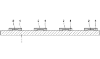
2 金属ライン、
3 構造体、
4 ポリマーライン。
Claims (34)
- 基底基板と、
前記基底基板上に配置され、ライン状に形成された金属より構成された層構造体と、
前記金属の層構造体上に配置された伝導性ポリマーの層構造体と、
を備え、
前記伝導性ポリマーの層構造体は、前記金属より構成された層構造体の少なくとも上面および一側面が覆われるように、ライン状に形成されることを特徴とする発光素子用の基板。 - 前記金属は、銀、銅、および金よりなる群から選択される何れか一種であることを特徴とする請求項1に記載の発光素子用の基板。
- 前記金属の層構造体は、ライン状に形成された複数の金属ラインより形成されたことを特徴とする請求項1または請求項2に記載の発光素子用の基板。
- 前記金属ラインは、50μmないし150μmの幅と10nmないし200nmの高さとを有し、隣接した金属ライン間の距離は、100μmないし1500μmであることを特徴とする請求項3に記載の発光素子用の基板。
- 前記伝導性ポリマーは、ポリエチレンジオキシチオフェンまたはポリアニリンであることを特徴とする請求項1〜請求項4のいずれか一項に記載の発光素子用の基板。
- 前記伝導性ポリマーの層構造体は、層厚が30nmないし300nmである連続層より形成されたことを特徴とする請求項1〜請求項5のいずれか一項に記載の発光素子用の基板。
- 前記伝導性ポリマーの層構造体は、ライン状に形成された複数のポリマーラインより形成されたことを特徴とする請求項1〜請求項6のいずれか一項に記載の発光素子用の基板。
- 前記ポリマーラインは、100μmないし400μmの幅と、10nmないし200nmの高さとを有し、隣接したポリマーライン間の距離は、100μmないし1500μmであることを特徴とする請求項7に記載の発光素子用の基板。
- 前記伝導性ポリマーの層構造体において、前記ポリマーラインは、前記金属ラインの少なくとも上面および一側面を覆うように形成されることを特徴とする請求項7または請求項8に記載の発光素子用の基板。
- 前記伝導性ポリマーの層構造体において、前記ポリマーラインは、前記金属ラインを完全に覆うことによって埋設されるように形成されることを特徴とする請求項7または請求項8に記載の発光素子用の基板。
- ライン状の金属の層構造体が伝導性ポリマーによって少なくとも上面および一側面を覆うように形成される、伝導性ポリマー構造体を有する発光素子用の基板の製造方法であって、
基底基板上に、50μmないし150μmの幅と10nmないし200nmの高さを有する金属層を付着するステップと、
100μmないし400μmの幅と10nmないし200nmの高さを有する、伝導性ポリマーの層構造体を付着するステップと、
を含むことを特徴とする発光素子用の基板の製造方法。 - 前記ライン状に付着された金属ラインは、金属を含むインクのインクジェットプリンティングにより付着されたことを特徴とする請求項11に記載の発光素子用の基板の製造方法。
- 前記伝導性ポリマーは、スピンコーティングまたはプリンティングにより付着されたことを特徴とする請求項11または請求項12に記載の発光素子用の基板の製造方法。
- 銀、銅、および金よりなる群から選択される何れか一種は、前記金属として使用され、
ポリエチレンジオキシチオフェンまたはポリアニリンは、前記伝導性ポリマーとして使用されることを特徴とする請求項11〜請求項13のいずれか一項に記載の発光素子用の基板の製造方法。 - 基底基板上に配置され、50μmないし150μmの幅と10nmないし200nmの高さとを有する金属より構成された層と、
前記金属の層構造体上に100μmないし400μmの幅と10nmないし200nmの高さを有する伝導性ポリマーの層と、
を備え、
前記金属層は、前記伝導性ポリマー層によって少なくとも上面および一側面が覆われるように、ライン状に形成されることを特徴とする発光素子用の電極。 - 前記金属は、銀、銅、および金よりなる群から選択される何れか一種であることを特徴とする請求項15に記載の発光素子用の電極。
- 前記金属層は、ライン状に形成された複数の金属ラインより形成されたことを特徴とする請求項15または請求項16に記載の発光素子用の電極。
- 前記金属ラインは、50μmないし150μmの幅と、10nmないし200nmの高さとを有し、隣接した金属ライン間の距離は、100μmないし1500μmであることを特徴とする請求項17に記載の発光素子用の電極。
- 前記伝導性ポリマーは、ポリエチレンジオキシチオフェンまたはポリアニリンであることを特徴とする請求項15〜請求項18のいずれか一項に記載の発光素子用の電極。
- 前記伝導性ポリマーの層構造体は、層厚が30nmないし300nmである連続層より形成されたことを特徴とする請求項15から請求項19のいずれか一項に記載の発光素子用の電極。
- 前記伝導性ポリマーの層構造体は、ライン状に形成された複数のポリマーラインより形成されたことを特徴とする請求項19または請求項20に記載の発光素子用の電極。
- 前記ポリマーラインは、100μmないし400μmの幅と、10nmないし200nmの高さとを有し、隣接したポリマーライン間の距離は、100μmないし1500μmであることを特徴とする請求項21に記載の発光素子用の電極。
- 前記伝導性ポリマーの層構造体において、前記ポリマーラインは、前記金属ラインの少なくとも上面および一側面を覆うように形成されることを特徴とする請求項21または請求項22に記載の発光素子用の電極。
- 前記伝導性ポリマー層構造体において、前記ポリマーラインは、前記金属ラインを完全に覆うことによって埋設するように形成されることを特徴とする請求項21〜請求項23いずれか一項に記載の発光素子用の電極。
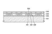
- 基底基板上に配置され、50μmないし150μmの幅と10nmないし200nmの高さとを有する金属より構成された層構造体、及び前記金属の層構造体上に配置された、100μmないし400μmの幅と10nmないし200nmの高さを有する伝導性ポリマーの層を備え、前記金属層は、前記伝導性ポリマー層によって少なくとも上面および一側面が覆われるように、ライン状に形成される伝導性ポリマー層構造体からなる第1電極と、
前記第1電極と対向された第2電極と、
前記第1電極と前記第2電極との間に介在される発光層と、を備えることを特徴とする発光素子。 - 前記金属は、銀、銅、および金よりなる群から選択される何れか一種であることを特徴とする請求項25に記載の発光素子。
- 前記金属の層構造体は、ライン状に形成された複数の金属ラインより形成されたことを特徴とする請求項25または請求項26に記載の発光素子。
- 前記金属ラインは、50μmないし150μmの幅と、10nmないし200nmの高さとを有し、隣接した金属ライン間の距離は、100μmないし1500μmであることを特徴とする請求項27に記載の発光素子。
- 前記伝導性ポリマーは、ポリエチレンジオキシチオフェンまたはポリアニリンであることを特徴とする請求項25〜請求項28のいずれか一項に記載の発光素子。
- 前記伝導性ポリマーの層構造体は、層厚が30nmないし300nmである連続層より形成されたことを特徴とする請求項25から請求項29のいずれか一項に記載の発光素子。
- 前記伝導性ポリマーの層構造体は、ライン状に形成された複数のポリマーラインより形成されたことを特徴とする請求項25から請求項30のいずれか一項に記載の発光素子。
- 前記ポリマーラインは、100μmないし400μmの幅と、10nmないし200nmの高さとを有し、隣接したポリマーライン間の距離は、100μmないし1500μmであることを特徴とする請求項31に記載の発光素子。
- 前記ポリマーラインは、前記金属ラインの少なくとも上面および一側面を覆うように形成されることを特徴とする請求項31または請求項32に記載の発光素子。
- 前記ポリマーラインは、前記金属ラインを完全に覆うことによって埋設するように形成されることを特徴とする請求項31または請求項32に記載の発光素子。
Applications Claiming Priority (4)
| Application Number | Priority Date | Filing Date | Title |
|---|---|---|---|
| EP04090368.4 | 2004-09-21 | ||
| EP04090368A EP1638155A1 (de) | 2004-09-21 | 2004-09-21 | Verbesserung der Leitfähigkeit einer Polymerelektrode durch Aufbringen einer darunterliegenden Metallschicht |
| KR10-2005-0018757 | 2005-03-07 | ||
| KR1020050018757A KR100622152B1 (ko) | 2004-09-21 | 2005-03-07 | 발광 소자용 기판, 그 제조 방법, 발광 소자용 전극 및 이를 구비한 발광 소자 |
Publications (2)
| Publication Number | Publication Date |
|---|---|
| JP2006093123A JP2006093123A (ja) | 2006-04-06 |
| JP4732084B2 true JP4732084B2 (ja) | 2011-07-27 |
Family
ID=36073252
Family Applications (1)
| Application Number | Title | Priority Date | Filing Date |
|---|---|---|---|
| JP2005261210A Active JP4732084B2 (ja) | 2004-09-21 | 2005-09-08 | 発光素子用の基板、その製造方法、発光素子用の電極、及びこれを備えた発光素子 |
Country Status (2)
| Country | Link |
|---|---|
| US (1) | US7710018B2 (ja) |
| JP (1) | JP4732084B2 (ja) |
Families Citing this family (21)
| Publication number | Priority date | Publication date | Assignee | Title |
|---|---|---|---|---|
| KR100966358B1 (ko) * | 2005-10-14 | 2010-06-28 | 샌디스크 코포레이션 | 비트라인 커플링을 나타내는 비휘발성 메모리를 제어프로그래밍하는 방법 |
| WO2007059577A1 (en) * | 2005-11-24 | 2007-05-31 | Newsouth Innovations Pty Limited | Metallisation method for thin-film semiconductor structures |
| US8138075B1 (en) | 2006-02-06 | 2012-03-20 | Eberlein Dietmar C | Systems and methods for the manufacture of flat panel devices |
| WO2007135604A2 (en) * | 2006-05-22 | 2007-11-29 | Philips Intellectual Property & Standards Gmbh | Interconnection arrangement and method for interconnecting a high-cuurent carrying cable with a metal thin-film |
| JP2008034367A (ja) * | 2006-07-04 | 2008-02-14 | Semiconductor Energy Lab Co Ltd | 表示装置 |
| US8974918B2 (en) | 2006-07-04 | 2015-03-10 | Semiconductor Energy Laboratory Co., Ltd. | Display device and electronic device |
| JP2008243557A (ja) * | 2007-03-27 | 2008-10-09 | Osaka Univ | 有機エレクトロルミネッセンス素子及びその製造方法 |
| DE102007024153A1 (de) * | 2007-04-23 | 2008-10-30 | Osram Opto Semiconductors Gmbh | Elektrisches organisches Bauelement und Verfahren zu seiner Herstellung |
| JP2010244868A (ja) * | 2009-04-07 | 2010-10-28 | Sony Corp | 有機電界発光素子および表示装置 |
| JP5565047B2 (ja) * | 2010-03-31 | 2014-08-06 | 大日本印刷株式会社 | 有機エレクトロルミネッセンス素子およびその製造方法 |
| WO2011125537A1 (ja) | 2010-04-05 | 2011-10-13 | コニカミノルタホールディングス株式会社 | 透明電極及びそれを用いた有機電子素子 |
| WO2011148931A1 (ja) * | 2010-05-28 | 2011-12-01 | コニカミノルタホールディングス株式会社 | 有機電子デバイス用電極 |
| US8865298B2 (en) | 2011-06-29 | 2014-10-21 | Eastman Kodak Company | Article with metal grid composite and methods of preparing |
| US8628840B2 (en) | 2011-06-29 | 2014-01-14 | Eastman Kodak Company | Electronically conductive laminate donor element |
| US9786865B2 (en) | 2013-04-01 | 2017-10-10 | Pioneer Corporation | Optical device |
| US9825248B2 (en) | 2013-04-01 | 2017-11-21 | Pioneer Corporation | Optical device |
| US9831460B2 (en) | 2013-04-01 | 2017-11-28 | Pioneer Corporation | Optical device |
| CN103236504A (zh) | 2013-05-10 | 2013-08-07 | 合肥京东方光电科技有限公司 | 柔性基板及制造方法、oled显示装置 |
| JP6255796B2 (ja) | 2013-08-19 | 2018-01-10 | 凸版印刷株式会社 | 透明電極の製造方法、透明電極、及びそれを備えた有機エレクトロルミネッセンス素子の製造方法、有機エレクトロルミネッセンス素子 |
| JP2015138861A (ja) * | 2014-01-22 | 2015-07-30 | ソニー株式会社 | 固体撮像素子および製造方法、並びに電子機器 |
| JP2016162633A (ja) * | 2015-03-03 | 2016-09-05 | 凸版印刷株式会社 | 透明電極、及び有機エレクトロルミネッセンス素子 |
Citations (1)
| Publication number | Priority date | Publication date | Assignee | Title |
|---|---|---|---|---|
| WO2004019666A1 (en) * | 2002-08-22 | 2004-03-04 | Agfa-Gevaert | Process for preparing a substantially transparent conductive layer configuration |
Family Cites Families (15)
| Publication number | Priority date | Publication date | Assignee | Title |
|---|---|---|---|---|
| WO1997012276A1 (en) | 1995-09-25 | 1997-04-03 | Philips Electronics N.V. | Electroluminescent illumination system and a flat-panel picture display device provided with such a system |
| KR100635429B1 (ko) * | 1998-08-03 | 2006-10-18 | 듀폰 디스플레이즈, 인크. | 무기 재료를 사용한 중합체-기재 고체 장치의 캡슐화 |
| US7102280B1 (en) | 1999-11-29 | 2006-09-05 | Paulus Cornelis Duineveld | Organic electroluminescent device and a method of manufacturing thereof |
| US6372154B1 (en) * | 1999-12-30 | 2002-04-16 | Canon Kabushiki Kaisha | Luminescent ink for printing of organic luminescent devices |
| JP2002124391A (ja) | 2000-08-08 | 2002-04-26 | Seiko Precision Inc | Elシート |
| US6710541B2 (en) * | 2000-12-22 | 2004-03-23 | Reveo, Inc. | Polarized light sources and methods for making the same |
| WO2003001490A2 (en) * | 2001-06-25 | 2003-01-03 | Avery Dennison Corporation | Hybrid display device |
| JP4302914B2 (ja) * | 2001-07-30 | 2009-07-29 | 三星モバイルディスプレイ株式會社 | 発光素子、および表示装置 |
| JP2003133071A (ja) * | 2001-08-13 | 2003-05-09 | Victor Co Of Japan Ltd | 有機エレクトロルミネセンス素子及びその製造方法 |
| US6750608B2 (en) * | 2001-11-09 | 2004-06-15 | Konica Corporation | Organic electroluminescence element and display |
| JP4310984B2 (ja) * | 2002-02-06 | 2009-08-12 | 株式会社日立製作所 | 有機発光表示装置 |
| EP2249413A3 (en) * | 2002-04-01 | 2011-02-02 | Konica Corporation | Support and organic electroluminescence element comprising the support |
| JP2004172090A (ja) * | 2002-10-31 | 2004-06-17 | Seiko Epson Corp | エレクトロルミネッセンス装置の製造方法及びエレクトロルミネッセンス装置、並びに電子機器 |
| JP2004178930A (ja) * | 2002-11-26 | 2004-06-24 | Sony Corp | 発光素子およびこれを用いた表示装置 |
| JP4066802B2 (ja) * | 2002-12-17 | 2008-03-26 | 富士ゼロックス株式会社 | ポリエステル樹脂及びそれを用いた機能素子、有機電界発光素子、並びに有機電界発光素子の製造方法 |
-
2005
- 2005-09-08 JP JP2005261210A patent/JP4732084B2/ja active Active
- 2005-09-20 US US11/229,491 patent/US7710018B2/en active Active
Patent Citations (2)
| Publication number | Priority date | Publication date | Assignee | Title |
|---|---|---|---|---|
| WO2004019666A1 (en) * | 2002-08-22 | 2004-03-04 | Agfa-Gevaert | Process for preparing a substantially transparent conductive layer configuration |
| JP2006502535A (ja) * | 2002-08-22 | 2006-01-19 | アグフア−ゲヴエルト | 実質的に透明な伝導層構成の製造方法 |
Also Published As
| Publication number | Publication date |
|---|---|
| US20060061270A1 (en) | 2006-03-23 |
| US7710018B2 (en) | 2010-05-04 |
| JP2006093123A (ja) | 2006-04-06 |
Similar Documents
| Publication | Publication Date | Title |
|---|---|---|
| JP4732084B2 (ja) | 発光素子用の基板、その製造方法、発光素子用の電極、及びこれを備えた発光素子 | |
| JP5969450B2 (ja) | 有機発光ディスプレイ装置および有機発光ディスプレイ装置の製造方法 | |
| US8169132B2 (en) | Organic light emitting diode display device and method of manufacturing the same | |
| KR100647325B1 (ko) | 저면발광형 유기발광소자 | |
| US8653511B2 (en) | Organic light emitting diode display | |
| US8624259B2 (en) | Organic light-emitting display device | |
| TW201320328A (zh) | 有機發光顯示裝置及其製造方法 | |
| KR100719554B1 (ko) | 평판 디스플레이 장치 및 그 제조방법 | |
| US8455897B2 (en) | Organic light-emitting display apparatus and method of manufacturing the same | |
| US8247274B2 (en) | Organic light-emitting display apparatus and method of manufacturing the same | |
| US7714324B2 (en) | Organic thin film transistor and method of manufacturing the same | |
| KR100622152B1 (ko) | 발광 소자용 기판, 그 제조 방법, 발광 소자용 전극 및 이를 구비한 발광 소자 | |
| JP4622580B2 (ja) | 成膜方法及び有機化合物層 | |
| JP2006243127A (ja) | シートディスプレイ | |
| JP2007095518A (ja) | 有機エレクトロルミネッセンス表示装置 | |
| KR100937867B1 (ko) | 유기 발광 디스플레이 장치 | |
| KR100708750B1 (ko) | 유기 발광 디스플레이 장치의 제조방법 및 유기 발광디스플레이 장치 | |
| JP2006252876A (ja) | 有機化合物層の積層方法、エレクトロルミネッセンスディスプレイパネルの製造方法、エレクトロルミネッセンスディスプレイパネル | |
| KR20070025152A (ko) | 유기전계발광소자 및 그 제조 방법 | |
| JP2010238479A (ja) | 有機el素子及び有機el素子の製造方法 | |
| KR100708841B1 (ko) | 평판 표시 장치 및 그 제조방법 | |
| KR100637206B1 (ko) | 전계발광 디스플레이 장치 | |
| JP2005166485A (ja) | 有機エレクトロルミネッセンス装置とその製造方法、電子機器 | |
| WO2010092882A1 (ja) | 有機el発光装置 | |
| JP2010182700A (ja) | 成膜方法及びディスプレイパネル |
Legal Events
| Date | Code | Title | Description |
|---|---|---|---|
| A711 | Notification of change in applicant |
Free format text: JAPANESE INTERMEDIATE CODE: A712 Effective date: 20081201 |
|
| A131 | Notification of reasons for refusal |
Free format text: JAPANESE INTERMEDIATE CODE: A131 Effective date: 20090414 |
|
| A521 | Request for written amendment filed |
Free format text: JAPANESE INTERMEDIATE CODE: A523 Effective date: 20090714 |
|
| A521 | Request for written amendment filed |
Free format text: JAPANESE INTERMEDIATE CODE: A523 Effective date: 20091023 |
|
| RD02 | Notification of acceptance of power of attorney |
Free format text: JAPANESE INTERMEDIATE CODE: A7422 Effective date: 20091023 |
|
| A521 | Request for written amendment filed |
Free format text: JAPANESE INTERMEDIATE CODE: A821 Effective date: 20091023 |
|
| A02 | Decision of refusal |
Free format text: JAPANESE INTERMEDIATE CODE: A02 Effective date: 20100914 |
|
| A521 | Request for written amendment filed |
Free format text: JAPANESE INTERMEDIATE CODE: A523 Effective date: 20101224 |
|
| A911 | Transfer to examiner for re-examination before appeal (zenchi) |
Free format text: JAPANESE INTERMEDIATE CODE: A911 Effective date: 20110113 |
|
| TRDD | Decision of grant or rejection written | ||
| A01 | Written decision to grant a patent or to grant a registration (utility model) |
Free format text: JAPANESE INTERMEDIATE CODE: A01 Effective date: 20110329 |
|
| A61 | First payment of annual fees (during grant procedure) |
Free format text: JAPANESE INTERMEDIATE CODE: A61 Effective date: 20110420 |
|
| FPAY | Renewal fee payment (event date is renewal date of database) |
Free format text: PAYMENT UNTIL: 20140428 Year of fee payment: 3 |
|
| R150 | Certificate of patent or registration of utility model |
Ref document number: 4732084 Country of ref document: JP Free format text: JAPANESE INTERMEDIATE CODE: R150 Free format text: JAPANESE INTERMEDIATE CODE: R150 |
|
| FPAY | Renewal fee payment (event date is renewal date of database) |
Free format text: PAYMENT UNTIL: 20140428 Year of fee payment: 3 |
|
| S111 | Request for change of ownership or part of ownership |
Free format text: JAPANESE INTERMEDIATE CODE: R313115 |
|
| FPAY | Renewal fee payment (event date is renewal date of database) |
Free format text: PAYMENT UNTIL: 20140428 Year of fee payment: 3 |
|
| R371 | Transfer withdrawn |
Free format text: JAPANESE INTERMEDIATE CODE: R371 |
|
| S111 | Request for change of ownership or part of ownership |
Free format text: JAPANESE INTERMEDIATE CODE: R313115 |
|
| FPAY | Renewal fee payment (event date is renewal date of database) |
Free format text: PAYMENT UNTIL: 20140428 Year of fee payment: 3 |
|
| R350 | Written notification of registration of transfer |
Free format text: JAPANESE INTERMEDIATE CODE: R350 |
|
| R250 | Receipt of annual fees |
Free format text: JAPANESE INTERMEDIATE CODE: R250 |
|
| R250 | Receipt of annual fees |
Free format text: JAPANESE INTERMEDIATE CODE: R250 |
|
| R250 | Receipt of annual fees |
Free format text: JAPANESE INTERMEDIATE CODE: R250 |
|
| R250 | Receipt of annual fees |
Free format text: JAPANESE INTERMEDIATE CODE: R250 |
|
| R250 | Receipt of annual fees |
Free format text: JAPANESE INTERMEDIATE CODE: R250 |
|
| R250 | Receipt of annual fees |
Free format text: JAPANESE INTERMEDIATE CODE: R250 |
|
| R250 | Receipt of annual fees |
Free format text: JAPANESE INTERMEDIATE CODE: R250 |
|
| R250 | Receipt of annual fees |
Free format text: JAPANESE INTERMEDIATE CODE: R250 |
|
| R250 | Receipt of annual fees |
Free format text: JAPANESE INTERMEDIATE CODE: R250 |
|
| R250 | Receipt of annual fees |
Free format text: JAPANESE INTERMEDIATE CODE: R250 |
|
| R250 | Receipt of annual fees |
Free format text: JAPANESE INTERMEDIATE CODE: R250 |