JP5093361B2 - ESD protection device and manufacturing method thereof - Google Patents
ESD protection device and manufacturing method thereof Download PDFInfo
- Publication number
- JP5093361B2 JP5093361B2 JP2010540330A JP2010540330A JP5093361B2 JP 5093361 B2 JP5093361 B2 JP 5093361B2 JP 2010540330 A JP2010540330 A JP 2010540330A JP 2010540330 A JP2010540330 A JP 2010540330A JP 5093361 B2 JP5093361 B2 JP 5093361B2
- Authority
- JP
- Japan
- Prior art keywords
- insulating layer
- cavity
- esd protection
- auxiliary electrode
- protection device
- Prior art date
- Legal status (The legal status is an assumption and is not a legal conclusion. Google has not performed a legal analysis and makes no representation as to the accuracy of the status listed.)
- Active
Links
- 238000004519 manufacturing process Methods 0.000 title claims description 75
- 239000004020 conductor Substances 0.000 claims description 211
- 239000000758 substrate Substances 0.000 claims description 186
- 239000010410 layer Substances 0.000 claims description 151
- 239000000843 powder Substances 0.000 claims description 140
- 239000002245 particle Substances 0.000 claims description 109
- 239000000919 ceramic Substances 0.000 claims description 106
- 239000000463 material Substances 0.000 claims description 98
- 238000000034 method Methods 0.000 claims description 64
- 239000007772 electrode material Substances 0.000 claims description 63
- 239000011521 glass Substances 0.000 claims description 61
- 238000010304 firing Methods 0.000 claims description 53
- 239000011810 insulating material Substances 0.000 claims description 29
- 229910010293 ceramic material Inorganic materials 0.000 claims description 26
- 238000012546 transfer Methods 0.000 claims description 20
- 239000002356 single layer Substances 0.000 claims description 9
- 230000008569 process Effects 0.000 claims description 5
- 230000000149 penetrating effect Effects 0.000 claims description 3
- 238000007789 sealing Methods 0.000 claims description 3
- 238000010030 laminating Methods 0.000 claims description 2
- 239000012811 non-conductive material Substances 0.000 claims description 2
- 230000001681 protective effect Effects 0.000 claims 1
- 239000010949 copper Substances 0.000 description 56
- VZSRBBMJRBPUNF-UHFFFAOYSA-N 2-(2,3-dihydro-1H-inden-2-ylamino)-N-[3-oxo-3-(2,4,6,7-tetrahydrotriazolo[4,5-c]pyridin-5-yl)propyl]pyrimidine-5-carboxamide Chemical compound C1C(CC2=CC=CC=C12)NC1=NC=C(C=N1)C(=O)NCCC(N1CC2=C(CC1)NN=N2)=O VZSRBBMJRBPUNF-UHFFFAOYSA-N 0.000 description 52
- 239000011347 resin Substances 0.000 description 49
- 229920005989 resin Polymers 0.000 description 49
- 239000003566 sealing material Substances 0.000 description 36
- 230000000052 comparative effect Effects 0.000 description 34
- PNEYBMLMFCGWSK-UHFFFAOYSA-N aluminium oxide Inorganic materials [O-2].[O-2].[O-2].[Al+3].[Al+3] PNEYBMLMFCGWSK-UHFFFAOYSA-N 0.000 description 32
- 230000004044 response Effects 0.000 description 27
- 229910052751 metal Inorganic materials 0.000 description 26
- 239000002184 metal Substances 0.000 description 26
- 230000015572 biosynthetic process Effects 0.000 description 24
- 230000004048 modification Effects 0.000 description 22
- 238000012986 modification Methods 0.000 description 22
- 239000002003 electrode paste Substances 0.000 description 19
- 239000000203 mixture Substances 0.000 description 17
- 238000007650 screen-printing Methods 0.000 description 17
- 150000002739 metals Chemical class 0.000 description 16
- RYGMFSIKBFXOCR-UHFFFAOYSA-N Copper Chemical compound [Cu] RYGMFSIKBFXOCR-UHFFFAOYSA-N 0.000 description 14
- AFCARXCZXQIEQB-UHFFFAOYSA-N N-[3-oxo-3-(2,4,6,7-tetrahydrotriazolo[4,5-c]pyridin-5-yl)propyl]-2-[[3-(trifluoromethoxy)phenyl]methylamino]pyrimidine-5-carboxamide Chemical compound O=C(CCNC(=O)C=1C=NC(=NC=1)NCC1=CC(=CC=C1)OC(F)(F)F)N1CC2=C(CC1)NN=N2 AFCARXCZXQIEQB-UHFFFAOYSA-N 0.000 description 14
- 229910052759 nickel Inorganic materials 0.000 description 14
- 230000004043 responsiveness Effects 0.000 description 14
- HMUNWXXNJPVALC-UHFFFAOYSA-N 1-[4-[2-(2,3-dihydro-1H-inden-2-ylamino)pyrimidin-5-yl]piperazin-1-yl]-2-(2,4,6,7-tetrahydrotriazolo[4,5-c]pyridin-5-yl)ethanone Chemical compound C1C(CC2=CC=CC=C12)NC1=NC=C(C=N1)N1CCN(CC1)C(CN1CC2=C(CC1)NN=N2)=O HMUNWXXNJPVALC-UHFFFAOYSA-N 0.000 description 13
- 238000007747 plating Methods 0.000 description 13
- 229920000178 Acrylic resin Polymers 0.000 description 12
- 239000004925 Acrylic resin Substances 0.000 description 12
- 239000000654 additive Substances 0.000 description 12
- 230000000996 additive effect Effects 0.000 description 12
- 239000002775 capsule Substances 0.000 description 12
- 239000002904 solvent Substances 0.000 description 12
- 239000011324 bead Substances 0.000 description 11
- 238000004381 surface treatment Methods 0.000 description 11
- MKYBYDHXWVHEJW-UHFFFAOYSA-N N-[1-oxo-1-(2,4,6,7-tetrahydrotriazolo[4,5-c]pyridin-5-yl)propan-2-yl]-2-[[3-(trifluoromethoxy)phenyl]methylamino]pyrimidine-5-carboxamide Chemical compound O=C(C(C)NC(=O)C=1C=NC(=NC=1)NCC1=CC(=CC=C1)OC(F)(F)F)N1CC2=C(CC1)NN=N2 MKYBYDHXWVHEJW-UHFFFAOYSA-N 0.000 description 10
- NIPNSKYNPDTRPC-UHFFFAOYSA-N N-[2-oxo-2-(2,4,6,7-tetrahydrotriazolo[4,5-c]pyridin-5-yl)ethyl]-2-[[3-(trifluoromethoxy)phenyl]methylamino]pyrimidine-5-carboxamide Chemical compound O=C(CNC(=O)C=1C=NC(=NC=1)NCC1=CC(=CC=C1)OC(F)(F)F)N1CC2=C(CC1)NN=N2 NIPNSKYNPDTRPC-UHFFFAOYSA-N 0.000 description 10
- 239000011230 binding agent Substances 0.000 description 10
- 239000004065 semiconductor Substances 0.000 description 10
- YXFVVABEGXRONW-UHFFFAOYSA-N Toluene Chemical compound CC1=CC=CC=C1 YXFVVABEGXRONW-UHFFFAOYSA-N 0.000 description 9
- 238000009413 insulation Methods 0.000 description 9
- 229910052763 palladium Inorganic materials 0.000 description 9
- 229910052697 platinum Inorganic materials 0.000 description 9
- 229910052709 silver Inorganic materials 0.000 description 9
- LDXJRKWFNNFDSA-UHFFFAOYSA-N 2-(2,4,6,7-tetrahydrotriazolo[4,5-c]pyridin-5-yl)-1-[4-[2-[[3-(trifluoromethoxy)phenyl]methylamino]pyrimidin-5-yl]piperazin-1-yl]ethanone Chemical compound C1CN(CC2=NNN=C21)CC(=O)N3CCN(CC3)C4=CN=C(N=C4)NCC5=CC(=CC=C5)OC(F)(F)F LDXJRKWFNNFDSA-UHFFFAOYSA-N 0.000 description 8
- 239000012298 atmosphere Substances 0.000 description 8
- 239000011248 coating agent Substances 0.000 description 8
- 238000000576 coating method Methods 0.000 description 8
- 229910052802 copper Inorganic materials 0.000 description 8
- 238000002156 mixing Methods 0.000 description 8
- 108091008695 photoreceptors Proteins 0.000 description 8
- 238000005245 sintering Methods 0.000 description 8
- 239000011800 void material Substances 0.000 description 8
- 229910018072 Al 2 O 3 Inorganic materials 0.000 description 7
- 239000000853 adhesive Substances 0.000 description 7
- 230000001070 adhesive effect Effects 0.000 description 7
- 239000000956 alloy Substances 0.000 description 7
- 229910045601 alloy Inorganic materials 0.000 description 7
- 230000006866 deterioration Effects 0.000 description 7
- 230000006872 improvement Effects 0.000 description 7
- 239000012212 insulator Substances 0.000 description 7
- 229910052741 iridium Inorganic materials 0.000 description 7
- 230000002093 peripheral effect Effects 0.000 description 7
- 229910052703 rhodium Inorganic materials 0.000 description 7
- 150000003624 transition metals Chemical group 0.000 description 7
- YLZOPXRUQYQQID-UHFFFAOYSA-N 3-(2,4,6,7-tetrahydrotriazolo[4,5-c]pyridin-5-yl)-1-[4-[2-[[3-(trifluoromethoxy)phenyl]methylamino]pyrimidin-5-yl]piperazin-1-yl]propan-1-one Chemical compound N1N=NC=2CN(CCC=21)CCC(=O)N1CCN(CC1)C=1C=NC(=NC=1)NCC1=CC(=CC=C1)OC(F)(F)F YLZOPXRUQYQQID-UHFFFAOYSA-N 0.000 description 6
- 229910004298 SiO 2 Inorganic materials 0.000 description 6
- MCMNRKCIXSYSNV-UHFFFAOYSA-N Zirconium dioxide Chemical compound O=[Zr]=O MCMNRKCIXSYSNV-UHFFFAOYSA-N 0.000 description 6
- 238000010586 diagram Methods 0.000 description 6
- 238000002844 melting Methods 0.000 description 6
- 230000008018 melting Effects 0.000 description 6
- 239000007769 metal material Substances 0.000 description 6
- 239000002002 slurry Substances 0.000 description 6
- 239000001856 Ethyl cellulose Substances 0.000 description 5
- ZZSNKZQZMQGXPY-UHFFFAOYSA-N Ethyl cellulose Chemical compound CCOCC1OC(OC)C(OCC)C(OCC)C1OC1C(O)C(O)C(OC)C(CO)O1 ZZSNKZQZMQGXPY-UHFFFAOYSA-N 0.000 description 5
- 238000001354 calcination Methods 0.000 description 5
- 230000007547 defect Effects 0.000 description 5
- 229920001249 ethyl cellulose Polymers 0.000 description 5
- 235000019325 ethyl cellulose Nutrition 0.000 description 5
- 229910010272 inorganic material Inorganic materials 0.000 description 5
- 239000011147 inorganic material Substances 0.000 description 5
- 239000000047 product Substances 0.000 description 5
- 230000006641 stabilisation Effects 0.000 description 5
- 238000011105 stabilization Methods 0.000 description 5
- 238000003756 stirring Methods 0.000 description 5
- 229910052718 tin Inorganic materials 0.000 description 5
- NIXOWILDQLNWCW-UHFFFAOYSA-N acrylic acid group Chemical group C(C=C)(=O)O NIXOWILDQLNWCW-UHFFFAOYSA-N 0.000 description 4
- 230000015556 catabolic process Effects 0.000 description 4
- 230000007423 decrease Effects 0.000 description 4
- 230000000694 effects Effects 0.000 description 4
- 238000003475 lamination Methods 0.000 description 4
- 239000012508 resin bead Substances 0.000 description 4
- 230000003746 surface roughness Effects 0.000 description 4
- OKTJSMMVPCPJKN-UHFFFAOYSA-N Carbon Chemical compound [C] OKTJSMMVPCPJKN-UHFFFAOYSA-N 0.000 description 3
- 229910052799 carbon Inorganic materials 0.000 description 3
- 239000011247 coating layer Substances 0.000 description 3
- 239000002131 composite material Substances 0.000 description 3
- 238000000354 decomposition reaction Methods 0.000 description 3
- 238000006731 degradation reaction Methods 0.000 description 3
- 238000007606 doctor blade method Methods 0.000 description 3
- 230000005611 electricity Effects 0.000 description 3
- 229910052839 forsterite Inorganic materials 0.000 description 3
- HCWCAKKEBCNQJP-UHFFFAOYSA-N magnesium orthosilicate Chemical compound [Mg+2].[Mg+2].[O-][Si]([O-])([O-])[O-] HCWCAKKEBCNQJP-UHFFFAOYSA-N 0.000 description 3
- 239000012299 nitrogen atmosphere Substances 0.000 description 3
- 239000003960 organic solvent Substances 0.000 description 3
- 238000000206 photolithography Methods 0.000 description 3
- 239000004014 plasticizer Substances 0.000 description 3
- -1 polypropylene Polymers 0.000 description 3
- 238000007639 printing Methods 0.000 description 3
- 239000002994 raw material Substances 0.000 description 3
- 230000009467 reduction Effects 0.000 description 3
- 238000000926 separation method Methods 0.000 description 3
- 230000003068 static effect Effects 0.000 description 3
- 238000009834 vaporization Methods 0.000 description 3
- 230000008016 vaporization Effects 0.000 description 3
- 229920002799 BoPET Polymers 0.000 description 2
- ZTQSAGDEMFDKMZ-UHFFFAOYSA-N Butyraldehyde Chemical compound CCCC=O ZTQSAGDEMFDKMZ-UHFFFAOYSA-N 0.000 description 2
- 239000004743 Polypropylene Substances 0.000 description 2
- VYPSYNLAJGMNEJ-UHFFFAOYSA-N Silicium dioxide Chemical compound O=[Si]=O VYPSYNLAJGMNEJ-UHFFFAOYSA-N 0.000 description 2
- 229910052782 aluminium Inorganic materials 0.000 description 2
- 239000005388 borosilicate glass Substances 0.000 description 2
- 238000009826 distribution Methods 0.000 description 2
- 230000036039 immunity Effects 0.000 description 2
- 239000011368 organic material Substances 0.000 description 2
- 230000035515 penetration Effects 0.000 description 2
- 229920000728 polyester Polymers 0.000 description 2
- 229920000098 polyolefin Polymers 0.000 description 2
- 229920001155 polypropylene Polymers 0.000 description 2
- 238000012360 testing method Methods 0.000 description 2
- 229910052721 tungsten Inorganic materials 0.000 description 2
- QPLDLSVMHZLSFG-UHFFFAOYSA-N Copper oxide Chemical compound [Cu]=O QPLDLSVMHZLSFG-UHFFFAOYSA-N 0.000 description 1
- PPBRXRYQALVLMV-UHFFFAOYSA-N Styrene Natural products C=CC1=CC=CC=C1 PPBRXRYQALVLMV-UHFFFAOYSA-N 0.000 description 1
- 239000006096 absorbing agent Substances 0.000 description 1
- 239000007864 aqueous solution Substances 0.000 description 1
- NWXHSRDXUJENGJ-UHFFFAOYSA-N calcium;magnesium;dioxido(oxo)silane Chemical compound [Mg+2].[Ca+2].[O-][Si]([O-])=O.[O-][Si]([O-])=O NWXHSRDXUJENGJ-UHFFFAOYSA-N 0.000 description 1
- 230000008859 change Effects 0.000 description 1
- 238000002485 combustion reaction Methods 0.000 description 1
- 230000008602 contraction Effects 0.000 description 1
- 229910052878 cordierite Inorganic materials 0.000 description 1
- 238000002788 crimping Methods 0.000 description 1
- JSKIRARMQDRGJZ-UHFFFAOYSA-N dimagnesium dioxido-bis[(1-oxido-3-oxo-2,4,6,8,9-pentaoxa-1,3-disila-5,7-dialuminabicyclo[3.3.1]nonan-7-yl)oxy]silane Chemical compound [Mg++].[Mg++].[O-][Si]([O-])(O[Al]1O[Al]2O[Si](=O)O[Si]([O-])(O1)O2)O[Al]1O[Al]2O[Si](=O)O[Si]([O-])(O1)O2 JSKIRARMQDRGJZ-UHFFFAOYSA-N 0.000 description 1
- 229910052637 diopside Inorganic materials 0.000 description 1
- 230000008034 disappearance Effects 0.000 description 1
- 239000002270 dispersing agent Substances 0.000 description 1
- 238000005516 engineering process Methods 0.000 description 1
- 230000003628 erosive effect Effects 0.000 description 1
- 239000010433 feldspar Substances 0.000 description 1
- 238000011049 filling Methods 0.000 description 1
- 238000007646 gravure printing Methods 0.000 description 1
- 238000007641 inkjet printing Methods 0.000 description 1
- 230000001678 irradiating effect Effects 0.000 description 1
- 238000005304 joining Methods 0.000 description 1
- 229910052747 lanthanoid Inorganic materials 0.000 description 1
- 230000007257 malfunction Effects 0.000 description 1
- 238000005259 measurement Methods 0.000 description 1
- 239000000178 monomer Substances 0.000 description 1
- 239000012466 permeate Substances 0.000 description 1
- 229920000139 polyethylene terephthalate Polymers 0.000 description 1
- 239000005020 polyethylene terephthalate Substances 0.000 description 1
- 238000002360 preparation method Methods 0.000 description 1
- 239000000377 silicon dioxide Substances 0.000 description 1
- 235000013599 spices Nutrition 0.000 description 1
- 230000000087 stabilizing effect Effects 0.000 description 1
- 229920001909 styrene-acrylic polymer Polymers 0.000 description 1
- 239000000126 substance Substances 0.000 description 1
- 239000006228 supernatant Substances 0.000 description 1
- 238000010023 transfer printing Methods 0.000 description 1
- 238000001291 vacuum drying Methods 0.000 description 1
Images


Classifications
-
- H—ELECTRICITY
- H02—GENERATION; CONVERSION OR DISTRIBUTION OF ELECTRIC POWER
- H02H—EMERGENCY PROTECTIVE CIRCUIT ARRANGEMENTS
- H02H9/00—Emergency protective circuit arrangements for limiting excess current or voltage without disconnection
- H02H9/04—Emergency protective circuit arrangements for limiting excess current or voltage without disconnection responsive to excess voltage
-
- H—ELECTRICITY
- H01—ELECTRIC ELEMENTS
- H01T—SPARK GAPS; OVERVOLTAGE ARRESTERS USING SPARK GAPS; SPARKING PLUGS; CORONA DEVICES; GENERATING IONS TO BE INTRODUCED INTO NON-ENCLOSED GASES
- H01T4/00—Overvoltage arresters using spark gaps
- H01T4/10—Overvoltage arresters using spark gaps having a single gap or a plurality of gaps in parallel
- H01T4/12—Overvoltage arresters using spark gaps having a single gap or a plurality of gaps in parallel hermetically sealed
-
- H—ELECTRICITY
- H01—ELECTRIC ELEMENTS
- H01T—SPARK GAPS; OVERVOLTAGE ARRESTERS USING SPARK GAPS; SPARKING PLUGS; CORONA DEVICES; GENERATING IONS TO BE INTRODUCED INTO NON-ENCLOSED GASES
- H01T21/00—Apparatus or processes specially adapted for the manufacture or maintenance of spark gaps or sparking plugs
-
- H—ELECTRICITY
- H01—ELECTRIC ELEMENTS
- H01T—SPARK GAPS; OVERVOLTAGE ARRESTERS USING SPARK GAPS; SPARKING PLUGS; CORONA DEVICES; GENERATING IONS TO BE INTRODUCED INTO NON-ENCLOSED GASES
- H01T4/00—Overvoltage arresters using spark gaps
- H01T4/10—Overvoltage arresters using spark gaps having a single gap or a plurality of gaps in parallel
-
- H—ELECTRICITY
- H02—GENERATION; CONVERSION OR DISTRIBUTION OF ELECTRIC POWER
- H02H—EMERGENCY PROTECTIVE CIRCUIT ARRANGEMENTS
- H02H9/00—Emergency protective circuit arrangements for limiting excess current or voltage without disconnection
- H02H9/04—Emergency protective circuit arrangements for limiting excess current or voltage without disconnection responsive to excess voltage
- H02H9/044—Physical layout, materials not provided for elsewhere
-
- H—ELECTRICITY
- H05—ELECTRIC TECHNIQUES NOT OTHERWISE PROVIDED FOR
- H05K—PRINTED CIRCUITS; CASINGS OR CONSTRUCTIONAL DETAILS OF ELECTRIC APPARATUS; MANUFACTURE OF ASSEMBLAGES OF ELECTRICAL COMPONENTS
- H05K9/00—Screening of apparatus or components against electric or magnetic fields
- H05K9/0067—Devices for protecting against damage from electrostatic discharge
-
- H—ELECTRICITY
- H05—ELECTRIC TECHNIQUES NOT OTHERWISE PROVIDED FOR
- H05K—PRINTED CIRCUITS; CASINGS OR CONSTRUCTIONAL DETAILS OF ELECTRIC APPARATUS; MANUFACTURE OF ASSEMBLAGES OF ELECTRICAL COMPONENTS
- H05K9/00—Screening of apparatus or components against electric or magnetic fields
- H05K9/0069—Methods for measuring the shielding efficiency; Apparatus therefor; Isolation container for testing
-
- H—ELECTRICITY
- H05—ELECTRIC TECHNIQUES NOT OTHERWISE PROVIDED FOR
- H05K—PRINTED CIRCUITS; CASINGS OR CONSTRUCTIONAL DETAILS OF ELECTRIC APPARATUS; MANUFACTURE OF ASSEMBLAGES OF ELECTRICAL COMPONENTS
- H05K9/00—Screening of apparatus or components against electric or magnetic fields
- H05K9/0073—Shielding materials
- H05K9/0079—Electrostatic discharge protection, e.g. ESD treated surface for rapid dissipation of charges
-
- H—ELECTRICITY
- H01—ELECTRIC ELEMENTS
- H01B—CABLES; CONDUCTORS; INSULATORS; SELECTION OF MATERIALS FOR THEIR CONDUCTIVE, INSULATING OR DIELECTRIC PROPERTIES
- H01B1/00—Conductors or conductive bodies characterised by the conductive materials; Selection of materials as conductors
- H01B1/20—Conductive material dispersed in non-conductive organic material
-
- Y—GENERAL TAGGING OF NEW TECHNOLOGICAL DEVELOPMENTS; GENERAL TAGGING OF CROSS-SECTIONAL TECHNOLOGIES SPANNING OVER SEVERAL SECTIONS OF THE IPC; TECHNICAL SUBJECTS COVERED BY FORMER USPC CROSS-REFERENCE ART COLLECTIONS [XRACs] AND DIGESTS
- Y10—TECHNICAL SUBJECTS COVERED BY FORMER USPC
- Y10T—TECHNICAL SUBJECTS COVERED BY FORMER US CLASSIFICATION
- Y10T29/00—Metal working
- Y10T29/49—Method of mechanical manufacture
- Y10T29/49002—Electrical device making
Landscapes
- Engineering & Computer Science (AREA)
- Microelectronics & Electronic Packaging (AREA)
- Manufacturing & Machinery (AREA)
- Thermistors And Varistors (AREA)
- Spark Plugs (AREA)
- Elimination Of Static Electricity (AREA)
Description
本発明は、ESD保護デバイス及びその製造方法に関し、詳しくは、絶縁性基板の空洞部内に放電電極が対向して配置されたESD保護デバイスについて、放電開始電圧等のESD特性及び信頼性を向上する技術に関する。 The present invention relates to an ESD protection device and a method for manufacturing the same, and more particularly, to improve ESD characteristics such as a discharge start voltage and reliability of an ESD protection device in which discharge electrodes are arranged to face each other in a cavity of an insulating substrate. Regarding technology.
ESD(Electro-Static Discharge;静電気放電)とは、帯電した導電性の物体(人体等)が、他の導電性の物体(電子機器等)に接触、あるいは充分接近したときに、激しい放電が発生する現象である。ESDにより電子機器の損傷や誤作動などの問題が発生する。これを防ぐためには、放電時に発生する過大な電圧が電子機器の回路に加わらないようにする必要がある。このような用途に使用されるのがESD保護デバイスであり、サージ吸収素子やサージアブソーバとも呼ばれている。 ESD (Electro-Static Discharge) means that when a charged conductive object (human body, etc.) is in contact with or sufficiently close to another conductive object (electronic device, etc.) It is a phenomenon. ESD causes problems such as damage and malfunction of electronic devices. In order to prevent this, it is necessary to prevent an excessive voltage generated during discharge from being applied to the circuit of the electronic device. An ESD protection device is used for such an application, and is also called a surge absorbing element or a surge absorber.
ESD保護デバイスは、例えば回路の信号線路とグランド(接地)との間に配置する。ESD保護デバイスは、一対の放電電極を離間して対向させた構造であるので、通常の使用状態では高い抵抗を持っており、信号がグランド側に流れることはない。これに対し、例えば携帯電話等のアンテナから静電気が加わる場合のように、過大な電圧が加わると、ESD保護デバイスの放電電極間で放電が起こり、静電気をグランド側に導くことができる。これにより、ESDデバイスよりも後段の回路には、静電気による電圧が印加されず、回路を保護することができる。 The ESD protection device is disposed, for example, between a signal line of a circuit and a ground (ground). Since the ESD protection device has a structure in which a pair of discharge electrodes are spaced apart from each other, the ESD protection device has a high resistance in a normal use state, and no signal flows to the ground side. On the other hand, when an excessive voltage is applied, for example, when static electricity is applied from an antenna such as a mobile phone, a discharge occurs between the discharge electrodes of the ESD protection device, and the static electricity can be guided to the ground side. Thereby, a voltage due to static electricity is not applied to a circuit subsequent to the ESD device, and the circuit can be protected.
例えば図37の分解斜視図及び図38の断面図に示すESD保護デバイスは、絶縁性セラミックシート2が積層されるセラミック多層基板7内に空洞部5が形成され、外部電極1と導通した放電電極6が空洞部5内に対向配置され、空洞部5に放電ガスが閉じ込められている。放電電極6間で絶縁破壊を起こす電圧が印加されると、空洞部5内において放電電極6間で放電が起こり、その放電により過剰な電圧をグランドへ導き、後段の回路を保護することができる(例えば、特許文献1参照)。
For example, the ESD protection device shown in the exploded perspective view of FIG. 37 and the cross-sectional view of FIG. 38 is a discharge electrode in which a
しかし、このようなESD保護デバイスでは、放電電極間の間隔のばらつきによって、ESDに対する放電応答性(ESD応答性)が変動し易い。また、放電電極が対向する領域の面積によってESD応答性を調整する必要があるが、その調整には製品サイズ等による制限のため、所望とするESD応答性を実現しにくい場合がある。 However, in such an ESD protection device, the discharge responsiveness (ESD responsiveness) to ESD is likely to vary due to the variation in the interval between the discharge electrodes. Moreover, although it is necessary to adjust ESD responsiveness according to the area of the area | region which a discharge electrode opposes, it is difficult to implement | achieve desired ESD responsiveness for the adjustment because of restrictions by a product size.
本発明が解決しようとする第1の課題は、かかる実情に鑑み、ESD特性の調整や安定化が容易であるESD保護デバイス及びその製造方法を提供することである。 The first problem to be solved by the present invention is to provide an ESD protection device that can easily adjust and stabilize the ESD characteristics, and a method for manufacturing the same, in view of such circumstances.
また、例えば、後述する比較例2のように放電電極の間に導電材料が分散した構成により、効率的に放電現象を生じさせることが考えられる。しかし、このような構成では、放電時の衝撃で導電材料が飛散して分布密度が低下するため、放電後に放電電圧が徐々に高くなってしまい、繰り返し放電により放電特性が劣化する。 Further, for example, it is conceivable that a discharge phenomenon is efficiently generated by a configuration in which a conductive material is dispersed between discharge electrodes as in Comparative Example 2 described later. However, in such a configuration, the conductive material scatters due to an impact at the time of discharge and the distribution density decreases, so that the discharge voltage gradually increases after discharge, and the discharge characteristics deteriorate due to repeated discharge.
本発明が解決しようとする第2の課題は、は、かかる実情に鑑み、ESD特性の調整や安定化が容易であり、繰り返し放電による放電特性の劣化を防止することができるESD保護デバイス及びその製造方法を提供することである。 The second problem to be solved by the present invention is that an ESD protection device capable of easily adjusting and stabilizing the ESD characteristics and preventing the deterioration of the discharge characteristics due to repeated discharges, and its It is to provide a manufacturing method.
また、このようなESD保護デバイスでは、次のような問題点がある。 Such an ESD protection device has the following problems.
第1に、放電開始電圧の設定は、主に放電電極間の間隔を調整することにより行う。しかし、デバイスの作製バラツキや、焼成時におけるセラミック多層基板と放電電極との収縮挙動の差などにより、放電電極間隔がばらつき、ESD保護デバイスの放電開始電圧がばらつきやすい。そのため、放電開始電圧を精度よく設定することができない。 First, the setting of the discharge start voltage is performed mainly by adjusting the interval between the discharge electrodes. However, due to variations in device fabrication, differences in shrinkage behavior between the ceramic multilayer substrate and the discharge electrode during firing, the discharge electrode spacing varies, and the discharge start voltage of the ESD protection device tends to vary. Therefore, the discharge start voltage cannot be set with high accuracy.
第2に、空洞部にある放電電極は、空洞部の気密性の低下や、セラミック多層基板の基材層と放電電極との熱膨張率(「熱膨張係数」ともいう。)の差などにより、セラミック多層基板から剥離することがある。そのような場合には、ESD保護デバイスとして機能しなくなったり、放電開始電圧が変化したりして、ESD保護デバイスの信頼性が低下する。 Secondly, the discharge electrode in the cavity part is caused by a decrease in the airtightness of the cavity part or a difference in thermal expansion coefficient (also referred to as “thermal expansion coefficient”) between the base material layer of the ceramic multilayer substrate and the discharge electrode. , May peel from the ceramic multilayer substrate. In such a case, the device does not function as an ESD protection device, or the discharge start voltage changes, and the reliability of the ESD protection device decreases.
本発明が解決しようとする第3の課題は、かかる実情に鑑み、放電開始電圧を精度よく設定することができ、信頼性の高いESD保護デバイス及びその製造方法を提供することである。 The third problem to be solved by the present invention is to provide a highly reliable ESD protection device and a method for manufacturing the same, in which the discharge start voltage can be set with high accuracy in view of such a situation.
本発明は、上記第1の課題を解決するために、以下のように構成したESD保護デバイスを提供する。 In order to solve the first problem, the present invention provides an ESD protection device configured as follows.
ESD保護デバイスは、(a)絶縁性基板と、(b)前記絶縁性基板の内部に形成された空洞部と、(c)前記空洞部内に露出して対向する露出部分を有する、少なくとも一対の放電電極と、(d)前記絶縁性基板の表面に形成され、前記放電電極と接続された外部電極とを有する。前記空洞部内において前記放電電極の前記露出部分の間に、導電性を有する粉状の補助電極材料が分散している。前記空洞部内に絶縁材料が分散している。 The ESD protection device has at least a pair of (a) an insulating substrate, (b) a cavity formed inside the insulating substrate, and (c) an exposed portion that is exposed and opposed to the cavity. A discharge electrode; and (d) an external electrode formed on the surface of the insulating substrate and connected to the discharge electrode. A conductive powdery auxiliary electrode material is dispersed between the exposed portions of the discharge electrode in the cavity. An insulating material is dispersed in the cavity.
上記構成において、対向する放電電極の露出部分の間に導電性を有する補助電極材料が分散しているので、空洞部内において電子の移動が起こりやすく、より効率的に放電現象を生じさせることができる。そのため、放電電極の間隔のばらつきによるESD応答性の変動を小さくすることができる。 In the above configuration, since the conductive auxiliary electrode material is dispersed between the exposed portions of the opposing discharge electrodes, electrons easily move in the cavity, and a discharge phenomenon can be generated more efficiently. . Therefore, the variation in the ESD response due to the variation in the interval between the discharge electrodes can be reduced.
また、空洞部内に分散させる補助電極材料の量や粒径等を調整することによって、容易に所望とするESD特性(放電開始電圧等)を得ることができる。 Moreover, desired ESD characteristics (discharge start voltage, etc.) can be easily obtained by adjusting the amount and particle size of the auxiliary electrode material dispersed in the cavity.
したがって、ESD特性の調整や安定化を図ることができる。
補助電極材料同士の接触が、空洞部内に分散されている絶縁材料によって阻止される。そのため、隣接する補助電極材料同士の接触に起因して放電電極間でショートが発生することを防止できる。
Therefore, the ESD characteristics can be adjusted and stabilized.
Contact between the auxiliary electrode materials is prevented by the insulating material dispersed in the cavity. Therefore, it is possible to prevent a short circuit from occurring between the discharge electrodes due to contact between adjacent auxiliary electrode materials.
好ましくは、前記補助電極材料は、絶縁材料により被覆されている。 Preferably, the auxiliary electrode material is covered with an insulating material.
この場合、補助電極材料が絶縁材料によって被覆されているので、隣接する補助電極材料同士の接触に起因して放電電極間でショートが発生することを防止できる。 In this case, since the auxiliary electrode material is covered with the insulating material, it is possible to prevent a short circuit from occurring between the discharge electrodes due to contact between adjacent auxiliary electrode materials.
また、空洞部内における放電現象は、絶縁体と空間との間の沿面にて発生する沿面放電が発生し易い。補助電極材料を絶縁材料により被覆することによって、空洞部内により多くの沿面を形成することができるため、よりESD応答性を高めることができる。 In addition, the discharge phenomenon in the cavity is likely to generate creeping discharge that occurs on the creeping surface between the insulator and the space. By covering the auxiliary electrode material with an insulating material, more creepage surfaces can be formed in the cavity, so that ESD response can be further improved.
さらに、補助電極材料が絶縁材料で被覆された粒の間の隙間を微少にすることで、気中放電によるロスを低減し、放電特性の劣化を低減することができる。 Furthermore, by reducing the gap between the grains in which the auxiliary electrode material is coated with the insulating material, loss due to air discharge can be reduced, and deterioration of discharge characteristics can be reduced.
好ましくは、前記絶縁性基板がセラミック基板である。 Preferably, the insulating substrate is a ceramic substrate.
この場合、ESD保護デバイスの作製が容易である。 In this case, it is easy to produce an ESD protection device.
好ましくは、前記セラミック基板はガラス成分を含有する。前記セラミック基板と前記空洞部との間に、前記セラミック基板中の前記ガラス成分が前記空洞部に浸透する。 Preferably, the ceramic substrate contains a glass component. Between the ceramic substrate and the cavity, the glass component in the ceramic substrate penetrates into the cavity.
この場合、シール部材によって、セラミック基板中のガラス成分が空洞部に浸透することを防止することができるため、空洞部に浸透したガラス成分によって空洞部内の補助電極材料がネッキングすることを抑制することができる。 In this case, since the sealing member can prevent the glass component in the ceramic substrate from penetrating into the cavity, it is possible to prevent the auxiliary electrode material in the cavity from being necked by the glass component that has penetrated into the cavity. Can do.
また、空洞部に浸透したガラス成分が補助電極材料を被覆している絶縁材料や補助電極材料間に分散された絶縁材料を侵食して放電電極間の絶縁性を低下させることを、防止することができる。 In addition, the glass component that has penetrated into the cavity is prevented from eroding the insulating material covering the auxiliary electrode material or the insulating material dispersed between the auxiliary electrode materials, thereby reducing the insulation between the discharge electrodes. Can do.
上記第2の課題を解決するため、好ましくは、前記補助電極材料は、前記空洞部内において前記放電電極の間に分散された導電材料であり、当該導電材料は前記空洞部を形成する底面及び天面に接している。 In order to solve the second problem, preferably, the auxiliary electrode material is a conductive material dispersed between the discharge electrodes in the cavity, and the conductive material includes a bottom surface and a ceiling that form the cavity. It touches the surface.
上記構成において、外部電極間に所定以上の大きさの電圧が印加されると、対向する放電電極の露出部分の間で放電が発生する。この放電は、主に、空洞部の空間と絶縁性基板との界面に沿って発生する沿面放電である。この沿面放電が発生する界面、すなわち空洞部を形成する底面及び天面に分散された導電材料が接しているので、電子の移動が起こりやすく、より効率的に放電現象を生じさせ、ESD応答性を高めることができる。そのため、放電電極間の間隔のばらつきによるESD応答性の変動を小さくしたりすることができる。したがって、ESD特性の調整や安定化が容易になる。 In the above configuration, when a voltage of a predetermined level or larger is applied between the external electrodes, a discharge is generated between the exposed portions of the opposing discharge electrodes. This discharge is a creeping discharge generated mainly along the interface between the space of the cavity and the insulating substrate. Since the dispersed conductive material is in contact with the interface where the creeping discharge occurs, that is, the bottom surface and the top surface forming the cavity, the electrons easily move, causing the discharge phenomenon more efficiently, and the ESD response. Can be increased. Therefore, it is possible to reduce the variation in the ESD response due to the variation in the interval between the discharge electrodes. Therefore, adjustment and stabilization of the ESD characteristics are facilitated.
また、空洞部を形成する底面及び天面の両方に沿面放電を生じさせる導電材料が接しているので、一方側だけに導電材料が分散されている場合と比べると、よりESD応答性を高めることができる。 In addition, since the conductive material that causes creeping discharge is in contact with both the bottom surface and the top surface that form the cavity, the ESD response can be further improved compared to the case where the conductive material is dispersed only on one side. Can do.
さらに、導電材料は空洞部を形成する底面及び天面と接しているので、基板本体からの導電材料の離脱が防止される。そのため、放電現象が繰り返されることによるESD特性の劣化(例えば、放電開始電圧の上昇等)を抑制することができる。 Furthermore, since the conductive material is in contact with the bottom surface and the top surface that form the cavity, the conductive material is prevented from being detached from the substrate body. Therefore, it is possible to suppress degradation of ESD characteristics (for example, increase in discharge start voltage) due to repeated discharge phenomena.
好ましくは、前記導電材料は、前記導電材料の一部が前記絶縁性基板に埋設されている。 Preferably, in the conductive material, a part of the conductive material is embedded in the insulating substrate.
この場合、導電材料が絶縁性基板に接しているのみならず埋設されているため、より効果的に絶縁性基板からの導電材料の離脱を抑制することができる。 In this case, since the conductive material is buried as well as being in contact with the insulating substrate, the detachment of the conductive material from the insulating substrate can be more effectively suppressed.
好ましくは、前記絶縁性基板は、セラミック材料とガラス材料とを含むセラミック基板である。前記導電材料は、前記ガラス材料によって前記絶縁性基板に固着されている。 Preferably, the insulating substrate is a ceramic substrate including a ceramic material and a glass material. The conductive material is fixed to the insulating substrate by the glass material.
この場合、導電材料は、絶縁性基板に接しているのみならず、ガラス材料によって固着されているため、より効果的に絶縁性基板からの導電材料の離脱を抑制することができる。 In this case, since the conductive material is not only in contact with the insulating substrate but is fixed by the glass material, the separation of the conductive material from the insulating substrate can be more effectively suppressed.
また、空洞部を形成する内周面にガラス材料によってガラス層が形成されると、空洞部を形成する内周面の表面粗さが低下する。そのため、沿面放電する際に電子が走る距離が短くなり、ESD応答性をさらに向上させることができる。 Further, when a glass layer is formed of a glass material on the inner peripheral surface forming the cavity, the surface roughness of the inner peripheral surface forming the cavity is reduced. Therefore, the distance traveled by electrons during creeping discharge is shortened, and the ESD response can be further improved.
上記第3の課題を解決するため、好ましくは、前記放電電極の前記露出部分の間の前記空洞部を形成する内面に沿って、前記補助電極材料である導電材料の粉体が、厚み方向に導電材料の粉体の粒子を1個だけを含む一層に配置されてなる、補助電極部が形成されている。 In order to solve the third problem, preferably, the powder of the conductive material that is the auxiliary electrode material is arranged in the thickness direction along the inner surface that forms the cavity between the exposed portions of the discharge electrode. An auxiliary electrode portion is formed which is arranged in a single layer containing only one conductive material powder particle.
上記構成において、補助電極部の導電材料の粉体は、空洞部を形成する内面から後退して配置され空洞部内には全く露出しない状態であっても、空洞部を形成する内面から空洞部内に突出し空洞部内に露出する部分があってもよい。 In the above configuration, the conductive material powder of the auxiliary electrode portion is disposed so as to recede from the inner surface forming the cavity and is not exposed at all in the cavity. There may be a portion that protrudes and is exposed in the cavity.
上記構成において、補助電極部の導電材料の粉体は、均一な密度で配置されてもよいし、例えば、一列又は複数列の帯状や、網目状、散点状など、密度を変えて配置されてもよい。 In the above configuration, the conductive material powder of the auxiliary electrode portion may be arranged at a uniform density, for example, arranged in a single or a plurality of rows of strips, meshes, dots, etc., with different densities. May be.
上記構成によれば、補助電極部の導電材料の量や種類などを調整することにより、放電開始電圧を所望の値に設定することができる。これにより、放電開始電圧は、放電電極の対向部間の間隔を変えることだけで調整する場合よりも、精度よく設定することができる。放電電極の導電材料の粉体が、厚み方向に導電材料の粉体の粒子を1個だけを含む一層に配置されているため、放電電極の導電材料の粉体同士の接触確率が低下し、放電電極間のショート発生を抑制し、ショート耐性を向上させることができる。 According to the above configuration, the discharge start voltage can be set to a desired value by adjusting the amount and type of the conductive material of the auxiliary electrode portion. Thereby, the discharge start voltage can be set with higher accuracy than the case where the discharge start voltage is adjusted only by changing the interval between the facing portions of the discharge electrode. Since the conductive material powder of the discharge electrode is arranged in a layer including only one conductive material powder particle in the thickness direction, the probability of contact between the conductive material powder of the discharge electrode decreases, Generation | occurrence | production of the short between discharge electrodes can be suppressed and short circuit tolerance can be improved.
また、放電電極の材料と同一又は類似である導電材料を用いて補助電極部を空洞部の内面に沿って形成することによって、放電電極間の領域において放電電極との収縮挙動や熱膨張率の差を緩和することができる。これによって、放電電極の剥離等による不良や特性バラツキ、特性の経年変化を小さくすることができる。 Further, by forming the auxiliary electrode portion along the inner surface of the cavity using a conductive material that is the same as or similar to the material of the discharge electrode, the contraction behavior and thermal expansion coefficient of the discharge electrode in the region between the discharge electrodes can be reduced. The difference can be mitigated. As a result, it is possible to reduce defects due to peeling of the discharge electrodes, characteristic variations, and changes in characteristics over time.
好ましくは、前記補助電極部の導電材料の粉体の少なくとも一部が、前記空洞部を形成する前記内面から前記空洞部内に露出している。 Preferably, at least a part of the powder of the conductive material of the auxiliary electrode portion is exposed in the cavity from the inner surface forming the cavity.
この場合、放電電極の導電材料を露出させることで、沿面放電がより促進され、放電開始電圧の低下、ESD応答性の向上など、ESD特性の向上をもたらす。 In this case, by exposing the conductive material of the discharge electrode, the creeping discharge is further promoted, and the ESD characteristics are improved, such as the reduction of the discharge start voltage and the improvement of the ESD response.
好ましくは、前記補助電極部の導電材料の粉体が、非導電性材料により被覆されている。 Preferably, the conductive material powder of the auxiliary electrode portion is coated with a non-conductive material.
この場合、補助電極部の導電材料の粉体同士の接触を防止し易くなる。 In this case, it becomes easy to prevent contact between the powders of the conductive material of the auxiliary electrode portion.
好ましくは、前記補助電極部は、前記絶縁性基板と前記放電電極との界面に沿って形成された部分を含む。 Preferably, the auxiliary electrode portion includes a portion formed along an interface between the insulating substrate and the discharge electrode.
上記構成によれば、放電電極の露出部分間の所定領域のみに補助電極部を形成する場合と比べ、補助電極部と放電電極との位置合わせの精度を緩和することができ、放電開始電圧のばらつきも小さくなり、製造コストを低減できる。 According to the above configuration, compared with the case where the auxiliary electrode portion is formed only in a predetermined region between the exposed portions of the discharge electrode, the alignment accuracy between the auxiliary electrode portion and the discharge electrode can be relaxed, and the discharge start voltage Variations are also reduced and manufacturing costs can be reduced.
好ましくは、前記絶縁性基板はセラミック基板である。 Preferably, the insulating substrate is a ceramic substrate.
上記構成によれば、焼成時の収縮挙動が放電電極の材料と同一又は類似である導電材料を用いて補助電極部を空洞部の内面に沿って形成することによって、放電電極の露出部分間の領域付近において放電電極とセラミック基板との収縮挙動の差を緩和することができる。これによって、焼成時における放電電極の剥離等による不良や特性バラツキを小さくすることができる。また、放電電極の間隔のバラツキも小さくなるので、放電開始電圧のバラツキを小さくすることができる。 According to the above configuration, the auxiliary electrode portion is formed along the inner surface of the cavity portion using a conductive material whose shrinkage behavior during firing is the same as or similar to the material of the discharge electrode, so that between the exposed portions of the discharge electrode. In the vicinity of the region, the difference in shrinkage behavior between the discharge electrode and the ceramic substrate can be reduced. As a result, it is possible to reduce defects and characteristic variations caused by peeling of the discharge electrode during firing. In addition, since the variation in the interval between the discharge electrodes is reduced, the variation in the discharge start voltage can be reduced.
また、補助電極部付近の熱膨張率が、放電電極の熱膨張率とセラミック基板の熱膨張率との中間の値になるようにすることができる。これによって、放電電極とセラミック基板との熱膨張率の差を補助電極部で緩和することができ、放電電極の剥離等による不良や特性の経年変化を小さくすることができる。 Further, the coefficient of thermal expansion in the vicinity of the auxiliary electrode portion can be set to an intermediate value between the coefficient of thermal expansion of the discharge electrode and the coefficient of thermal expansion of the ceramic substrate. Thereby, the difference in coefficient of thermal expansion between the discharge electrode and the ceramic substrate can be alleviated by the auxiliary electrode part, and defects due to peeling of the discharge electrode and the secular change of characteristics can be reduced.
また、本発明は、上記第1の課題を解決するため、以下のように構成したESD保護デバイスの製造方法を提供する。 In order to solve the first problem, the present invention provides a method for manufacturing an ESD protection device configured as follows.
ESD保護デバイスの製造方法は、(i)第一の絶縁層の一方主面と第二の絶縁層の一方主面との少なくとも一方に、間隔を設けて少なくとも一対の放電電極を形成する、第1の工程と、(ii)第一の絶縁層の一方主面と第二の絶縁層の一方主面との前記一方の前記放電電極の間に、導電性を有する補助電極材料を分散した状態で付着させる、第2の工程と、(iii)前記第一の絶縁層の前記一方主面と前記第二の絶縁層の前記一方主面とが互いに対向した状態で、前記第一の絶縁層と前記第二の絶縁層とを積層する、第3の工程と、(iv)前記第3の工程により得られた積層体の表面に、前記放電電極と接続された外部電極を形成する、第4の工程とを備える。前記積層体の内部において前記第一の絶縁層と前記第二の絶縁層との間に、前記一対の放電電極のそれぞれの一部が露出する空洞部が形成され、該空洞部内に前記補助電極材料が分散した状態で配置される。 A method for manufacturing an ESD protection device includes: (i) forming at least a pair of discharge electrodes with an interval provided on at least one of one main surface of the first insulating layer and one main surface of the second insulating layer; And (ii) a state in which a conductive auxiliary electrode material is dispersed between the one discharge electrode between the one main surface of the first insulating layer and the one main surface of the second insulating layer. And (iii) the first insulating layer with the one main surface of the first insulating layer and the one main surface of the second insulating layer facing each other. And (iv) forming an external electrode connected to the discharge electrode on the surface of the laminate obtained by the third step, and laminating the second insulating layer and the second insulating layer. 4 steps. A cavity is formed between the first insulating layer and the second insulating layer in the stacked body, and a part of each of the pair of discharge electrodes is exposed, and the auxiliary electrode is formed in the cavity. The material is arranged in a dispersed state.
上記方法によれば、空洞部内において対向する放電電極の間に補助電極材料が分散し、ESD特性の調整や安定化を図ることができる構成のESD保護デバイスを、容易に作製することができる。 According to the above method, it is possible to easily produce an ESD protection device having a configuration in which the auxiliary electrode material is dispersed between the discharge electrodes facing each other in the cavity, and the ESD characteristics can be adjusted and stabilized.
また、本発明は、上記第2の課題を解決するため、以下のように構成したESD保護デバイスの製造方法を提供する。 In order to solve the second problem, the present invention provides a method for manufacturing an ESD protection device configured as follows.
ESD保護デバイスの製造方法は、(i)第一の絶縁層の一方主面に、導電材料を分散した状態で付着させる、第1の工程と、(ii)前記第一の絶縁層の前記一方主面に、間隔を設けて少なくとも一対の放電電極を、該放電電極の間に前記第一の絶縁層の前記一方主面に付着された前記導電材料の少なくとも一部分が露出するように形成する、第2の工程と、(iii)前記第一の絶縁層の前記一方主面に、第二の絶縁層を、前記第二の絶縁層の一方主面が前記放電電極を被覆するとともに前記導電材料と接するように積層する、第3の工程と、(iv)前記第3の工程により得られた積層体の表面に、前記放電電極と接続された外部電極を形成する、第4の工程とを備える。前記第一の絶縁層の前記一方主面と前記第二の絶縁層の前記一方主面との間に空洞部が形成される。前記空洞部内に前記一対の放電電極のそれぞれの一部が露出する。前記空洞部内において前記導電材料が前記第一の絶縁層の前記一方主面と前記第二の絶縁層の前記一方主面とに接し、かつ前記導電材料の間に空隙が形成される。 The manufacturing method of the ESD protection device includes (i) a first step in which a conductive material is dispersedly attached to one main surface of the first insulating layer, and (ii) the one of the first insulating layers. Forming at least a pair of discharge electrodes on the main surface with an interval so that at least a part of the conductive material attached to the one main surface of the first insulating layer is exposed between the discharge electrodes; And (iii) the one main surface of the first insulating layer is covered with the second insulating layer, the one main surface of the second insulating layer covers the discharge electrode, and the conductive material. And (iv) a fourth step of forming an external electrode connected to the discharge electrode on the surface of the laminate obtained by the third step. Prepare. A cavity is formed between the one main surface of the first insulating layer and the one main surface of the second insulating layer. A part of each of the pair of discharge electrodes is exposed in the cavity. In the cavity, the conductive material is in contact with the one main surface of the first insulating layer and the one main surface of the second insulating layer, and a gap is formed between the conductive materials.
上記方法によれば、第一の絶縁層の一方主面と第二の絶縁層の一方主面とが、空洞部を形成する天面及び底面となり、空洞部を形成する天面及び底面に導電材料が接する構成を容易に形成することができる。 According to the above method, the one main surface of the first insulating layer and the one main surface of the second insulating layer become the top surface and the bottom surface forming the cavity, and the top surface and the bottom surface forming the cavity are electrically conductive. A structure in contact with the material can be easily formed.
好ましくは、前記第3の工程において、前記第一の絶縁層の前記一方主面に前記第二の絶縁層の前記一方主面が圧着されることにより、前記導電材料の一部が前記第一の絶縁層と前記第一の絶縁層とのいずれか一方又は両方に埋設される。 Preferably, in the third step, the one main surface of the second insulating layer is pressure-bonded to the one main surface of the first insulating layer, so that a part of the conductive material is the first main surface. Embedded in one or both of the insulating layer and the first insulating layer.
この場合、導電材料が絶縁性基板に接しているのみならず埋設されているため、より効果的に絶縁性基板からの導電材料の離脱を抑制することができる。 In this case, since the conductive material is buried as well as being in contact with the insulating substrate, the detachment of the conductive material from the insulating substrate can be more effectively suppressed.
好ましくは、前記第一の絶縁層及び前記第二の絶縁層はセラミック材料を主成分とする。前記第3の工程により得られた前記積層体を焼成する工程を備える。 Preferably, the first insulating layer and the second insulating layer are mainly composed of a ceramic material. A step of firing the laminate obtained by the third step.
この場合、セラミック多層基板と同様の製造方法で、ESD保護デバイスを容易に製造することができる。なお、積層体を焼成する工程は、第4の工程の前でも後でもよい。 In this case, the ESD protection device can be easily manufactured by the same manufacturing method as that for the ceramic multilayer substrate. Note that the step of firing the laminate may be before or after the fourth step.
好ましくは、前記積層体を焼成する工程において、前記積層体が積層方向に収縮することにより前記導電材料が前記第一の絶縁層と前記第二の絶縁層とのいずれか一方又は両方に埋設される。 Preferably, in the step of firing the laminated body, the conductive material is embedded in one or both of the first insulating layer and the second insulating layer by shrinking the laminated body in the stacking direction. The
この場合、セラミック材料を主成分とする第一の絶縁層及び第二の絶縁層の焼成時の収縮を利用して、導電材料を埋設することができる。 In this case, the conductive material can be embedded by utilizing the shrinkage during firing of the first insulating layer and the second insulating layer containing the ceramic material as a main component.
好ましくは、前記第一の絶縁層と前記第二の絶縁層とのいずれか一方又は両方は、ガラス材料を含有し、前記積層体を焼成する工程において当該絶縁層の前記一方主面のうち前記空洞部となるべき部分に対向する領域に前記ガラス材料によってガラス層が形成される。 Preferably, one or both of the first insulating layer and the second insulating layer contains a glass material, and the step of firing the laminated body includes the first main surface of the insulating layer. A glass layer is formed of the glass material in a region facing the portion to be the cavity.
この場合、ガラス材料の浸透を利用して、導電材料をより強固に絶縁層に固着させることができる。また、空洞部を形成する内周面の表面粗さが低下するため、沿面放電する際に電子が走る距離が短くなり、ESD応答性を向上させることができる。 In this case, the conductive material can be more firmly fixed to the insulating layer by utilizing the penetration of the glass material. In addition, since the surface roughness of the inner peripheral surface forming the hollow portion is reduced, the distance traveled by electrons during creeping discharge is shortened, and the ESD response can be improved.
好ましくは、前記第1の工程において、前記第一の絶縁層の前記一方主面に、前記導電材料とともに分散した空隙形成用材料を付着させる。前記第3の工程により得られた前記積層体から、前記空隙形成用材料を消失させることによって前記導電材料の間に前記空隙を形成する。 Preferably, in the first step, a gap forming material dispersed together with the conductive material is attached to the one main surface of the first insulating layer. The voids are formed between the conductive materials by eliminating the void forming material from the laminate obtained in the third step.
この場合、空隙形成用材料の消失によって導電材料の間に空隙を形成し、隣接する導電材料同士が接触して放電電極間でショートが発生することを防止できる。 In this case, voids are formed between the conductive materials due to the disappearance of the gap forming material, and adjacent conductive materials can be prevented from contacting each other and causing a short circuit between the discharge electrodes.
好ましくは、前記第1の工程において、前記導電材料及び前記空隙形成用材料を混合した状態で、前記第一の絶縁層の前記一方主面に付着させる。 Preferably, in the first step, the conductive material and the gap forming material are mixed and adhered to the one main surface of the first insulating layer.
この場合、導電材料が分散した状態で空洞内に配置されるようにすることが容易である。 In this case, it is easy to dispose the conductive material in the cavity in a dispersed state.
好ましくは、前記第1の工程において、前記導電材料を含む荷電性粉末と前記空隙形成用材料を含む荷電性粉末の混合材料を、電子写真法によって前記第一の絶縁層の前記一方主面に付着させる。 Preferably, in the first step, a mixed material of the charged powder containing the conductive material and the charged powder containing the gap forming material is applied to the one main surface of the first insulating layer by electrophotography. Adhere.
この場合、均一に分散した導電材料と空隙形成用材料とを第一の絶縁層の一方主面に付着させることができる。そのため、導電材料間の間隔を確実に保ち、安定したESD応答性を実現することができる。 In this case, the uniformly dispersed conductive material and void forming material can be attached to one main surface of the first insulating layer. Therefore, the interval between the conductive materials can be reliably maintained and a stable ESD response can be realized.
好ましくは、前記混合材料中において、前記導電材料を含む前記荷電性粉末の含有率が20%以上、80%以下である。 Preferably, in the mixed material, the content of the charged powder containing the conductive material is 20% or more and 80% or less.
導電材料を含む荷電性粉末の含有率が20%以上であると、導電材料によって良好なESD特性を得ることが容易である。導電材料を含む荷電性粉末の含有率が80%以下であると、導電材料の間に十分な空隙を形成して放電電極間のショートを防ぐことが容易である。 When the content of the charged powder containing a conductive material is 20% or more, it is easy to obtain good ESD characteristics with the conductive material. When the content of the chargeable powder containing the conductive material is 80% or less, it is easy to form a sufficient gap between the conductive materials and prevent a short circuit between the discharge electrodes.
また、本発明は、上記第3の課題を解決するため、以下のように構成したESD保護デバイスの製造方法を提供する。 In order to solve the third problem, the present invention provides a method for manufacturing an ESD protection device configured as follows.
ESD保護デバイスの製造方法は、(i)第一の絶縁層の一方主面上に導電材料の粉体を、厚み方向に導電材料の粉体の粒子を1個だけを含む一層に配置して補助電極部を形成する、第1の工程と、(ii)前記第一の絶縁層の前記一方主面上に、少なくとも一対の放電電極を形成し、該放電電極の間に前記補助電極部の少なくとも一部を露出させる、第2の工程と、(iii)前記第一の絶縁層の前記一方主面上に、前記放電電極を被覆し、かつ、前記放電電極の間の前記補助電極部の少なくとも一部が露出する露出領域から離れて該露出領域を覆うように、第二の絶縁層を形成する、第3の工程と、(iv)前記第3の工程により得られた積層体の表面に、前記放電電極と接続された外部電極を形成する、第4の工程とを備える。前記第2の絶縁層と前記放電電極と前記露出領域とにより囲まれた空洞部が形成される。 In the manufacturing method of the ESD protection device, (i) the conductive material powder is disposed on one main surface of the first insulating layer, and the conductive material powder is disposed in a layer including only one conductive material powder particle in the thickness direction. A first step of forming an auxiliary electrode portion; and (ii) forming at least a pair of discharge electrodes on the one main surface of the first insulating layer, and forming the auxiliary electrode portion between the discharge electrodes. A second step of exposing at least a portion; and (iii) covering the discharge electrode on the one main surface of the first insulating layer and forming the auxiliary electrode portion between the discharge electrodes. A third step of forming a second insulating layer so as to cover the exposed region apart from at least a part of the exposed region, and (iv) a surface of the laminate obtained by the third step And a fourth step of forming an external electrode connected to the discharge electrode. A cavity surrounded by the second insulating layer, the discharge electrode, and the exposed region is formed.
上記方法によれば、導電材料の粉体が空洞部に露出した状態を容易に作製することができる。 According to the above method, it is possible to easily produce a state in which the powder of the conductive material is exposed in the cavity.
具体的には、以下のように種々の態様で形成する。 Specifically, it forms in various aspects as follows.
好ましくは、前記第2の工程において前記放電電極の間に露出させるべき前記補助電極部の少なくとも一部分の上に、消失材料を含む空洞部形成層を形成する。前記第3の工程において前記空洞部形成層の上にも前記第二の絶縁層を形成した後、前記空洞部形成層の少なくとも一部を消失させることにより、前記空洞部を形成する。 Preferably, a cavity forming layer containing a disappearing material is formed on at least a part of the auxiliary electrode portion to be exposed between the discharge electrodes in the second step. In the third step, after the second insulating layer is formed also on the cavity forming layer, at least a part of the cavity forming layer is eliminated to form the cavity.
好ましくは、前記第1の工程において、前記補助電極部は、厚み方向に導電材料の粉体の粒子を1個だけを含む一層に配置された導電材料の粉体を、前記第一の絶縁層上に転写することにより形成される。 Preferably, in the first step, the auxiliary electrode portion is formed of a conductive material powder disposed in a single layer including only one conductive material powder particle in the thickness direction. It is formed by transferring it upward.
好ましくは、前記第1の工程において、前記補助電極部は電子写真法により形成される。 Preferably, in the first step, the auxiliary electrode portion is formed by electrophotography.
好ましくは、前記第1の工程において、前記第一の絶縁層の一方主面上に、厚み方向に導電材料の粉体の粒子を1個だけを含む一層に配置される前記補助電極部の導電材料の粉体は、消失材料により被覆されている。 Preferably, in the first step, the conductivity of the auxiliary electrode portion disposed on one main surface of the first insulating layer in a single layer including only one particle of the powder of the conductive material in the thickness direction. The powder of material is coated with the disappearing material.
この場合、補助電極部の導電材料の粉体同士の接触を防止し易くなる。 In this case, it becomes easy to prevent contact between the powders of the conductive material of the auxiliary electrode portion.
本発明によれば、ESDデバイスのESD特性の調整や安定化が容易である。 According to the present invention, it is easy to adjust and stabilize the ESD characteristics of an ESD device.
また、本発明の好ましい一態様によれば、ESDデバイスのESD特性の調整や安定化が容易であり、繰り返し放電による放電特性の劣化を防止することができる。 Moreover, according to one preferable aspect of the present invention, it is easy to adjust and stabilize the ESD characteristics of the ESD device, and it is possible to prevent deterioration of the discharge characteristics due to repeated discharge.
また、本発明の好ましい他の態様によれば、放電開始電圧を精度よく設定することができ、信頼性が高いESD保護デバイスを作製することができる。 Moreover, according to another preferable aspect of the present invention, the discharge start voltage can be set with high accuracy, and a highly reliable ESD protection device can be manufactured.
以下、本発明の実施の形態について、図1〜図36を参照しながら説明する。 Hereinafter, embodiments of the present invention will be described with reference to FIGS.
<実施例1−1> 実施例1−1のESD保護デバイス10について、図1〜図6を参照しながら説明する。
<Example 1-1> The
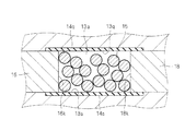
図1は、ESD保護デバイス10の断面図である。図1に示すように、ESD保護デバイス10は、セラミック基板の基板本体12の内部に空洞部13が形成されている。空洞部13内には、一対の放電電極16,18の先端16k,18k側が露出するように配置されている。放電電極16,18は、先端16k,18k同士が互いに間隔を設けて対向するように形成されている。放電電極16,18は、基板本体12の外周面まで延在し、基板本体12の表面に形成された外部電極22,24に接続されている。外部電極22,24は、ESD保護デバイス10を実装するために用いる。
FIG. 1 is a cross-sectional view of the
図1に模式的に示すように、空洞部13内には、導電性を有する粉状の補助電極材料30の表面が絶縁材料32で被覆された複数の補助電極粒15が配置されている。すなわち、空洞部13内には、導電性を有する粉状の補助電極材料30が分散している。
As schematically shown in FIG. 1, a plurality of
図2は、空洞部13の拡大断面図である。図2に模式的に示すように、空洞部13を形成する天面13p及び底面13sは、シール部材14p,14sによって形成されている。シール部材14p,14sは、基板本体12と空洞部13との間に延在し、セラミック基板である基板本体12中のガラス成分が空洞部13に浸透することを防止する。シール部材14p,14sは、絶縁性を有する。
FIG. 2 is an enlarged cross-sectional view of the
ESD保護デバイス10は、外部電極22,24間に所定以上の大きさの電圧が印加されると、空洞部13内において、対向する放電電極16,18間で放電が発生する。
In the
次に、ESD保護デバイス10の製造方法について、図3のイメージ図及び図4の概略図を参照しながら説明する。
Next, a method for manufacturing the
(1)材料の作製
まず、基板本体12、放電電極16,18、シール材14p,14sを形成するため材料を作製する。(1) Production of material First, a material is produced in order to form the
[セラミックグリーンシート]
基板本体12を形成するためのセラミックグリーンシートを作製する。セラミック材料には、Ba、Al、Siを中心とした組成からなる材料(BAS材)を用いる。各素材を所定の組成になるよう調合、混合し、800℃〜1000℃で仮焼して得られた仮焼粉末を、ジルコニアボールミルで12時間粉砕し、セラミック粉末を得る。このBAS材仮焼後セラミック粉末に、トルエン・エキネンなどの有機溶媒を加え混合する。さらにバインダー、可塑剤を加え混合し、スラリーを得る。このようにして得られたスラリーを、ドクターブレード法によりPETフィルム上へ成形し、任意の厚み(10μm〜50μm)のセラミックグリーンシートを得る。[Ceramic green sheet]
A ceramic green sheet for forming the
[電極ペースト]
放電電極16,18を形成するための電極ペーストを作製する。平均粒径約2μmのCu粉80wt%とエチルセルロース等からなるバインダー樹脂に溶剤を添加し、ロールで攪拌、混合することで、電極ペーストを得る。[Electrode paste]
An electrode paste for forming the
[シール材用ペースト]
シール材14p,14sを形成するためのシール材ペーストを、電極ペーストと同様の手法で作製する。平均粒径約1μmのAl2O3粉80wt%とエチルセルロース等からなるバインダー樹脂に溶剤を添加し、ロールで攪拌、混合することで、シール材用ペースト(アルミナペースト)を得る。シール材には、基板材料よりも焼結温度が高い材料を選定する。[Seal paste]
The sealing material paste for forming the sealing
(2)シール材形成
図4に示すように、セラミックグリーンシート11a,11bの一方主面である表面11p,11sに、スクリーン印刷にてシール材用ペースト(アルミナペースト)を塗布し、シール材14p,14sを形成する。シール材14p,14sは、放電電極16,18の先端16k,18k側を上下から挟むように配置するため、二層分作製する。(2) Sealing Material Formation As shown in FIG. 4, a sealing material paste (alumina paste) is applied to the
(3)放電電極形成
シール材14p,14sを形成したセラミックグリーンシート11a,11bの少なくも一方11bの表面11sに、スクリーン印刷法により、放電電極16,18を形成する。(3) Discharge electrode
作製例では、放電電極16,18の幅が100μm、放電ギャップ(対向する放電電極16,18の先端16k,18k間の距離)が30μmとなるように、帯状に放電電極16,18を形成した。
In the manufacturing example, the
(4)補助電極形成(補助電極材料の付着)
シール材14s及び放電電極16,18が形成されたセラミックグリーンシート11b上へ、スクリーン印刷法、もしくは電子写真法により図3にイメージを示すように補助電極材料30の表面が絶縁材料32で被覆されている補助電極粒15を付着させて、図4に示す補助電極形成層15kを形成する。(4) Auxiliary electrode formation (attachment of auxiliary electrode material)
The surface of the
(a)スクリーン印刷法による補助電極材料の付着
スクリーン印刷法による場合は、補助電極材料を含むペーストを作製し、作製したペーストを用いて補助電極形成層15kを形成することにより、補助電極材料を付着させる。(A) Adhesion of auxiliary electrode material by screen printing method When the screen printing method is used, an auxiliary electrode material is prepared by forming a paste containing the auxiliary electrode material and forming the auxiliary
補助電極粒15を含むペーストは、次の方法によって作製する。
The paste containing the
ペースト組成は、平均粒径約5μmのアルミナコートCu粉を所定の割合で調合し、バインダー樹脂と溶剤を添加し、ロールで攪拌、混合することで得る。ペースト中の樹脂と溶剤の比率は40wt%とする。アルミナコートCu粉は、焼成中に焼結しない。すなわち、ネッキングしない。アルミナコートCu粉は、焼成後も絶縁性を保つ。 The paste composition is obtained by preparing alumina-coated Cu powder having an average particle size of about 5 μm at a predetermined ratio, adding a binder resin and a solvent, stirring and mixing with a roll. The ratio of resin and solvent in the paste is 40 wt%. Alumina-coated Cu powder does not sinter during firing. That is, it does not neck. Alumina-coated Cu powder maintains insulation even after firing.
ペースト塗布量を制御することによって、空洞部13の高さを制御することができる。
By controlling the paste application amount, the height of the
(b)電子写真法による補助電極材料の付着
電子写真法により補助電極を形成する場合は、まず、補助電極粒15を含むトナーを作製し、作製したトナーを用いて補助電極形成層を形成する。(B) Adhesion of auxiliary electrode material by electrophotography When forming an auxiliary electrode by electrophotography, first, a toner including
[トナー作製]
トナーは次のように作製する。
1.アルミナコートCu粉(平均粒径5μm)と樹脂を混合し、表面処理機を用いてアルミナコートCu粉の表面に樹脂を被覆する。
2.上記1.のサンプルを分級し、微粉と粗粉を除去する。
3.上記2.の操作によって得られたカプセルCu粒と外添剤を混合し、表面処理機にてカプセルCu粒表面に外添剤を均一に付着させる。
4.上記3.の操作によって得られたカプセルCu紛とキャリアを混合し、現像剤となるトナーを得る。[Toner preparation]
The toner is prepared as follows.
1. Alumina-coated Cu powder (
2. Above 1. The sample is classified to remove fine powder and coarse powder.
3. 2. The capsule Cu particles obtained by the above operation and the external additive are mixed, and the external additive is uniformly adhered to the surface of the capsule Cu particles by a surface treatment machine.
4). 3. above. The capsule Cu powder obtained by the above operation and a carrier are mixed to obtain a toner as a developer.
[補助電極形成]
補助電極は次のように形成する。
1.感光体を一様に帯電させる。
2.帯電した感光体に、LEDにて補助電極の形状に光を照射し、潜像を形成する。
3.現像バイアスをかけ、感光体上にトナーを現像する。トナーの塗布量は、現像バイアスの大きさによって制御することができる。
4.補助電極のパターンが現像された感光体とセラミックグリーンシートを重ね、トナーをセラミックグリーンシート11bのシール材14s上に転写する。
5.補助電極のパターンが転写されたセラミックグリーンシートをオーブンに入れ、トナーを定着させ、補助電極のパターンが形成されたセラミックグリーンシートを得る。[Auxiliary electrode formation]
The auxiliary electrode is formed as follows.
1. The photoreceptor is charged uniformly.
2. The charged photoconductor is irradiated with light to the shape of the auxiliary electrode by an LED to form a latent image.
3. A developing bias is applied to develop the toner on the photoreceptor. The amount of toner applied can be controlled by the magnitude of the developing bias.
4). The photoreceptor on which the pattern of the auxiliary electrode is developed and the ceramic green sheet are overlapped, and the toner is transferred onto the sealing
5. The ceramic green sheet on which the auxiliary electrode pattern is transferred is placed in an oven to fix the toner, thereby obtaining a ceramic green sheet on which the auxiliary electrode pattern is formed.
なお、焼成後も補助電極自体は絶縁性を保った状態である。 Even after firing, the auxiliary electrode itself remains insulative.
(5)積層、圧着
図4において矢印11xで示すように、シール材14p,14sが形成されたセラミックグリーンシート11a,11bの表面11p,11sが互いに対向し、シール材14p,14sで補助電極形成層15kを挟むように、セラミックグリーンシート11a,11bを積層し、圧着して、積層体を形成する。(5) Lamination and pressure bonding As shown by an
作製例では、積層体の厚みが0.35mmとなり、その厚み方向の中央に放電電極と補助電極形成層とが配置されるように、セラミックグリーンシートを積層した。 In the production example, the ceramic green sheets were laminated so that the thickness of the laminate was 0.35 mm, and the discharge electrode and the auxiliary electrode forming layer were arranged in the center in the thickness direction.
(5)カット、端面電極塗布
ESD保護デバイスの複数個分を含むように積層体を形成する場合には、積層体を、LCフィルタのようなチップタイプの部品と同様に金型を用いて切断して、各チップの個片に分割する。作製例では1.0mm×0.5mmになるようにカットした。その後、各チップの端面に電極ペーストを塗布し、外部電極を形成する。(5) Cut, end face electrode application When forming a laminate to include multiple ESD protection devices, cut the laminate using a mold in the same way as chip-type components such as LC filters. Then, each chip is divided into individual pieces. In the production example, it was cut to be 1.0 mm × 0.5 mm. Thereafter, an electrode paste is applied to the end face of each chip to form external electrodes.
(6)焼成
外部電極を形成したチップを、通常のセラミック多層部品と同様に、N2雰囲気中で焼成する。セラミックグリーンシートの間に挟まれた補助電極形成層15k中の樹脂成分、溶剤成分は焼成時に消失し、これによって空洞部13の空間が形成される。(6) Firing The chip on which the external electrode is formed is fired in an N 2 atmosphere in the same manner as a normal ceramic multilayer component. The resin component and the solvent component in the auxiliary
ESDに対する応答電圧を下げるため空洞部13にAr、Neなどの希ガスを導入する場合には、セラミック材料の収縮、焼結が行われる温度領域をAr、Neなどの希ガス雰囲気で焼成すればよい。酸化しない電極材料(Agなど)の場合には、大気雰囲気でもかまわない。
When a rare gas such as Ar or Ne is introduced into the
(8)めっき
焼成後のチップの外部電極上に、LCフィルタのようなチップタイプの部品と同様に、電解Ni、Snメッキを行い、ESD保護デバイスが完成する。(8) Plating On the external electrode of the fired chip, electrolytic Ni and Sn plating is performed in the same manner as a chip type component such as an LC filter to complete an ESD protection device.
以上のように、セラミック基板を用いてESD保護デバイスを容易に作製することができる。 As described above, an ESD protection device can be easily manufactured using a ceramic substrate.
基板本体12のセラミック材料は、特に上記した材料に限定されるものでなく、絶縁性のものであればよいため、フォルステライトにガラスを加えたものや、CaZrO3にガラスを加えたものなど、他のものを用いてもよい。The ceramic material of the substrate
放電電極16,18の電極材料もCuだけでなく、Ag、Pd、Pt、Al、Ni、Wやこれらの組み合わせでもよい。
The electrode material of the
補助電極材料30は、Cuだけでなく、Ni、Co、Ag、Pd、Rh、Ru、Au、Pt、Ir等の遷移金属群より選ばれた少なくとも1種類の金属(導電材料)とすることが望ましい。また、これら金属を単体で用いてもよいが、合金として用いることも可能である。さらに、これらの金属の酸化物(抵抗材料)を用いてもよい。又は、SiCのような半導体材料でもよい。
The
また、これらの補助電極材料30の表面に、Al2O3、ZrO2、SiO2などの無機材料や、BASのような混合仮焼材料、高融点のガラスなどの絶遠材料32を被覆することにより、補助電極粒15を形成する。補助電極材料30の表面を被覆する絶縁材料32は、補助電極材料30の焼結を阻害するものであり、絶縁性を有する絶縁材料ならば、例示したもの以外でもよい。Further, the surface of the
補助電極材料30の平均粒子径は、0.05μm〜10μmの範囲が好ましい。より好ましい範囲は、1μm〜5μmである。粒子径が小さいほど表面積が大きくなり、放電開始電圧が低下し、ESDに対する応答特性が向上し、放電特性の劣化が低減する。
The average particle diameter of the
シール材14p,14sは、基板本体12に用いているセラミックよりも焼結温度が高いセラミック材料が好ましい。基板本体12からのガラスを遮断し、自身がガラスを生成しない絶縁物であればよく、窒化物などでもよい。
The sealing
実施例1−1のESD保護デバイス10は、空洞部13内に補助電極材料30が分散しているため、放電開始電圧の低下とESDに対する応答特性向上を得られる。
In the
すなわち、対向した電極間の放電現象は、空洞(気相)と基板(絶縁物)との境界を走る沿面放電が主に生じる(他の放電現象も起こる)。沿面放電とは、物(絶縁物)の表面を伝わって電流が流れる形態の放電現象である。電子が流れるといっても実際には、電子が表面をとび跳ね、気体のイオン化を生じ、移動すると考えられている。そして、絶縁物の表面に導電性粉末が存在すると電子の飛び跳ねる見かけ上の距離を縮め、方向性を持たせ、沿面放電現象をより積極的に生じさせる。 That is, the discharge phenomenon between the opposed electrodes is mainly a creeping discharge that runs along the boundary between the cavity (gas phase) and the substrate (insulator) (other discharge phenomena also occur). Creeping discharge is a discharge phenomenon in which a current flows through the surface of an object (insulator). Even though electrons flow, it is considered that electrons actually jump on the surface, cause gas ionization, and move. Then, when conductive powder is present on the surface of the insulator, the apparent distance at which electrons jump is shortened to have directionality, and a creeping discharge phenomenon is more actively generated.
実施例1−1のESD保護デバイス10では、対向する放電電極16,18間に、導電性を有する補助電極材料30の表面が絶縁材料32で被覆された補助電極粒15が分散され、充填されている。この補助電極粒15が配置されている部分、すなわち補助電極において、補助電極材料30は、焼成後も未焼結な状態、すなわちネッキングを起こしていない状態を維持している。放電補助材料30を含むそれぞれの補助電極粒15は、積み重ねられた状態、すなわち接触しただけの状態である。その結果、図6に示すように、補助電極粒15間には隙間15yが存在する。
In the
実施例1−1の構成では、積み上げられた補助電極粒15の表面、すなわち補助電極材料30の表面を被覆する絶縁材料32の表面と、隣接する補助電極粒15の間の隙間で沿面放電が生じる。実施例1−1では、図5の説明図において矢印82,84,86で示すように、沿面放電の経路が多数あることから、後述する比較例1より沿面放電が生じ易い。すなわち、より効率的に放電現象を生じさせることができる。そのため、放電電極16,18間の間隔を小さくしたり、放電電極16,18の間隔のばらつきによるESD応答性の変動を小さくすることができる。
In the configuration of Example 1-1, creeping discharge is generated in the gap between the surface of the stacked
また、実施例1−1の構成では補助電極粒15間の隙間が微少であることから、比較例1より、気中放電によるロスを低減する。そのため、比較例1より、放電特性の劣化を低減することができる。
Moreover, since the gap between the
また、空洞部内に分散させる補助電極材料の量や粒径等を調整することによって、容易に所望とするESD特性(放電開始電圧等)を得ることができる。 Moreover, desired ESD characteristics (discharge start voltage, etc.) can be easily obtained by adjusting the amount and particle size of the auxiliary electrode material dispersed in the cavity.
したがって、ESD特性の調整や安定化が容易である。 Therefore, adjustment and stabilization of the ESD characteristics are easy.
また、シール材14p,14sが存在することで、セラミックの基板本体12からのガラス成分の浸透を遮断する。そのため、補助電極材料30を被覆する絶縁材料32がガラス成分に浸食されて補助電極材料30の焼結が生じることや、補助電極材料30自体が基板本体12のセラミックヘ取り込まれることを防止する。その結果、補助電極粒15間の隙間を維持でき、ESD保護特性を向上させることができる。
Further, the presence of the sealing
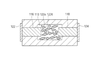
<比較例1> 比較例1のESD保護デバイス10xについて、図15〜図17を参照しながら説明する。
Comparative Example 1 An
図15は、ESD保護デバイス10xの断面図である。図16は、図15において鎖線で示した領域11を模式的に示す要部拡大断面図である。図17は放電の説明図である。
FIG. 15 is a cross-sectional view of the
図15に示すように、ESD保護デバイス10xは、実施例1−1と同様に、セラミック多層基板の基板本体12xの内部に空洞部13xが形成され、空洞部13x内に放電電極16,18の一部17,19が露出するようになっている。放電電極16,18は、基板本体12xの表面に形成された外部電極22,24に接続されている。
As shown in FIG. 15, in the
ESD保護デバイス10xは、実施例1−1と異なり、放電電極16,18の間の部分に隣接して、補助電極14xが形成されている。補助電極14xは、図16に示すように、基板本体12xを形成する絶縁材料中に金属材料20xが分散している部分であり、全体として絶縁性を有している。金属材料20xの一部は、空洞部13x内に露出している。補助電極14xは、例えば、セラミック材料と金属材料とを含む補助電極用ペーストをセラミックグリーンシートに塗布することにより形成する。
Unlike the example 1-1, the
比較例1では、図17において矢印80で示すように、補助電極14xと空洞部13xとの界面で沿面放電が生じる。
In Comparative Example 1, creeping discharge occurs at the interface between the
放電の衝撃で、空洞部13xに露出している補助電極14xの金属材料20xが離脱すると放電特性が劣化する。そのため、比較例1では放電特性が劣化しやすい。
When the
<作製例>
比較例1と実施例1−1のESD保護デバイスの作製例について、ESD保護特性を比較した。<Production example>
The ESD protection characteristics of the fabrication examples of the ESD protection device of Comparative Example 1 and Example 1-1 were compared.
具体的には、実施例1−1の作製例では、補助電極形成部をスクリーン印刷により形成した。比較例の作製例では、金属材料を含むペーストを用いスクリーン印刷により補助電極を形成した。実施例1−1の作製例と比較例1の作製例は、補助電極以外は同じ寸法・形状とし、焼成条件も同じとした。 Specifically, in the production example of Example 1-1, the auxiliary electrode forming portion was formed by screen printing. In the production example of the comparative example, the auxiliary electrode was formed by screen printing using a paste containing a metal material. The fabrication example of Example 1-1 and the fabrication example of Comparative Example 1 were the same size and shape except for the auxiliary electrode, and the firing conditions were also the same.
放電電極間のESDに対する放電応答性を100個ずつの試料にて評価した。ESDに対する放電応答性は、IECの規格、IEC61000−4−2に定められている、静電気放電イミュニティ試験によって行った。接触放電にて2kV〜8kv印加して試料の放電電極間で放電が生じるかどうかを調べた。 The discharge responsiveness to ESD between the discharge electrodes was evaluated for each of 100 samples. The discharge response to ESD was performed by an electrostatic discharge immunity test defined in IEC standard, IEC61000-4-2. It was investigated whether discharge occurred between the discharge electrodes of the sample by applying 2 kV to 8 kv by contact discharge.
比較結果を次の表1に示す。

表1から、空洞部内に補助電極材料が分散している実施例1−1の方が、金属材料が分散した補助電極が空洞部に隣接して形成されている比較例1より、ESDに対する放電応答性が優れており、ESD保護特性の向上を得られることが分かる。 From Table 1, in Example 1-1 in which the auxiliary electrode material is dispersed in the cavity, the discharge against ESD is more in comparison with Comparative Example 1 in which the auxiliary electrode in which the metal material is dispersed is formed adjacent to the cavity. It can be seen that the responsiveness is excellent and the ESD protection characteristics can be improved.
<変形例1−1> 変形例1−1について、図7及び図8を参照しながら説明する。 <Modification 1-1> Modification 1-1 will be described with reference to FIGS.
変形例1−1は、実施例1−1の変形例である。以下では、実施例1−1と同じ構成の部分には同じ符号を用い、実施例1−1との相違点を中心に説明する。 Modification 1-1 is a modification of Example 1-1. Below, the same code | symbol is used for the part of the structure same as Example 1-1, and it demonstrates centering around difference with Example 1-1.
図7は、変形例1−1のESD保護デバイス10aの断面図である。図8は、変形例1−1のESD保護デバイス10aの空洞部13aの要部拡大断面図である。
FIG. 7 is a cross-sectional view of the
図7及び図8に示すように、変形例1−1のESD保護デバイス10aは、補助電極材料が分散している空洞部13aの高さが、放電電極16,18の厚み程度になっている。すなわち、空洞部13aの天面13qを形成するシール材14qは平面状に延在している。
As shown in FIGS. 7 and 8, in the
沿面放電が最も生じ易いのは、セラミックの基板本体12と補助電極の境界部である。変形例1−1のESD保護デバイス10aは、空洞部13aの高さを低くすることで、放電電極16,18間をつなぐ境界部の距離が縮まるため、ESD保護特性のさらなる向上を得られる。
Creeping discharge is most likely to occur at the boundary between the
<実施例1−2> 実施例1−2のESD保護デバイスについて、図9及び図10を参照しながら説明する。 Example 1-2 An ESD protection device of Example 1-2 will be described with reference to FIGS. 9 and 10.
実施例1−2のESD保護デバイスは、実施例1−1のESD保護デバイス10と略同じ構成である。以下では、実施例1−1と同じ構成部分には同じ符号を用いて、実施例1−1との相違点を中心に説明する。
The ESD protection device of Example 1-2 has substantially the same configuration as the
図9は、空洞部13の要部拡大断面図である。図9に示すように、実施例1−2のESD保護デバイスは、空洞部13内に、補助電極材料を含有する補助電極粒15に加え、絶縁性を有する絶縁性粒15sも分散している点が、実施例1−1のESD保護デバイス10とは異なる。すなわち、補助電極粒15と絶縁性粒15sの混合体によって補助電極が形成される。空洞部内に配置され補助電極を形成する粒子15,15s同士は、未焼結な状態であり、絶縁を保った状態であればよい。
FIG. 9 is an enlarged cross-sectional view of the main part of the
補助電極粒15が含有する補助電極材料は、Cu、Ni、Co、Ag、Pd、Rh、Ru、Au、Pt、Ir等の遷移金属群より選ばれた少なくとも1種類の金属とすることが望ましい。また、これら金属を単体で用いてもよいが、合金として用いることも可能である。さらに、これらの金属の酸化物を用いてもよい。あるいは、補助電極粒の補助電極材料として、SiCのような半導体材料を用いてもよい。金属粒と半導体粒を混合して用いてもよい。
The auxiliary electrode material contained in the
実施例1−2では、補助電極粒15の間に絶縁性粒15sが介在することにより放電電極の絶縁性を確保することができるため、補助電極粒15は、導電性を有する補助電極材料のみで構成してもよい。
In Example 1-2, since the insulating property of the discharge electrode can be ensured by interposing the insulating
補助電極材料の表面を絶縁性材料で被覆した補助電極粒を用いると、放電電極の絶縁信頼性が向上するので好ましい。補助電極材料を被覆する絶縁材料には、導電性粉末の焼結を阻害させるためにAl2O3、ZrO2、SiO2などの無機材料、BASのような混合仮焼材料、高融点のガラスなど、絶縁性を有するコート材を用いる。Use of auxiliary electrode grains in which the surface of the auxiliary electrode material is coated with an insulating material is preferable because the insulation reliability of the discharge electrode is improved. The insulating material covering the auxiliary electrode material includes inorganic materials such as Al 2 O 3 , ZrO 2 , SiO 2 , mixed calcined materials such as BAS, and high melting point glass to inhibit sintering of the conductive powder. For example, an insulating coating material is used.
絶縁性粒15sは、補助電極粒15と焼結せず、絶縁性粒15s同士とも焼結しないものであればよい。例えば、基板の焼成温度よりも焼結温度が高いセラミック粉末(Al2O3、ZrO2、SiO2など)のような無機物が望ましい。The insulating
次に、実施例1−2のESD保護デバイスの製造方法について説明する。 Next, a method for manufacturing the ESD protection device of Example 1-2 will be described.
(1)材料の作製
基板本体を形成するためのセラミックグリーンシートと、放電電極を形成するための電極ペーストと、シール材を形成するためシール材用ペーストとを、実施例1−1に同じ方法で作製する。(1) Production of material The ceramic green sheet for forming the substrate body, the electrode paste for forming the discharge electrode, and the sealing material paste for forming the sealing material are the same as in Example 1-1. To make.
(2)シール材形成
シール材用ペーストを用いて、セラミックグリーンシート上にシール材を実施例1−1に同じ方法で形成する。(2) Formation of sealing material Using a sealing material paste, a sealing material is formed on the ceramic green sheet in the same manner as in Example 1-1.
(3)放電電極形成
電極用ペーストを用いて、セラミックグリーンシート上に放電電極を実施例1−1と同じ方法で形成する。(3) Discharge electrode formation Using the electrode paste, a discharge electrode is formed on the ceramic green sheet in the same manner as in Example 1-1.
(4)放電補助電極形成
シール材及び放電電極を形成したグリーンシート上へ、補助電極形成層をスクリーン印刷法、もしくは電子写真法により形成する。(4) Discharge auxiliary electrode formation An auxiliary electrode forming layer is formed on a green sheet on which a sealing material and a discharge electrode are formed by a screen printing method or an electrophotographic method.
(a)スクリーン印刷法による放電補助電極形成
スクリーン印刷法による場合は、補助電極粒と絶縁性粒とを含むペーストを作製し、作製したペーストを用いて、実施例1−1と同じ方法で補助電極形成層を形成する。(A) Discharge auxiliary electrode formation by screen printing method In the case of screen printing method, a paste containing auxiliary electrode grains and insulating grains is prepared, and the prepared paste is used to assist in the same manner as in Example 1-1. An electrode forming layer is formed.
補助電極粒と絶縁性粒とを含むペーストは、次の方法によって作製する。 A paste containing auxiliary electrode grains and insulating grains is prepared by the following method.
ペースト組成は、平均粒径約5μmのアルミナコートCu粒とアルミナ粒を所定の割合で調合し、バインダー樹脂と溶剤を添加し、ロールで攪拌、混合することで得る。アルミナコートCu粒とアルミナ粒は、体積比率で1:1とする。ペースト中の樹脂と溶剤の比率は40wt%とする。アルミナコートCu粉及びアルミナ粒は、焼成中に焼結しない。すなわち、ネッキングしない。アルミナコートCu粒及びアルミナ粒は、焼成後も焼成後も絶縁性を保つ。 The paste composition is obtained by preparing alumina-coated Cu particles and alumina particles having an average particle size of about 5 μm at a predetermined ratio, adding a binder resin and a solvent, stirring and mixing with a roll. The volume ratio of the alumina-coated Cu particles and the alumina particles is 1: 1. The ratio of resin and solvent in the paste is 40 wt%. Alumina-coated Cu powder and alumina particles are not sintered during firing. That is, it does not neck. Alumina-coated Cu grains and alumina grains maintain insulation properties both after firing and after firing.
(b)電子写真法による放電補助電極形成
電子写真法により補助電極を形成する場合は、補助電極粒と絶縁性粒とを含むトナーを作製し、作製したトナーを用いて、実施例1−1と同じ方法で補助電極形成層を形成する。(B) Discharge auxiliary electrode formation by electrophotography When forming an auxiliary electrode by electrophotography, a toner containing auxiliary electrode particles and insulating particles is prepared, and the prepared toner is used in Example 1-1. An auxiliary electrode forming layer is formed by the same method.
補助電極粒と絶縁性粒とを含むトナーは次のように作製する。
1.アルミナコートCu粒(平均粒径5μm)と樹脂を混合し、表面処理機を用いて銅粉表面に樹脂を被覆する。
2.上記1.のサンプルを分級し、微粉と粗粉を除去する。
3.上記2.の操作によって得られたカプセルCu粒と外添剤を混合し、表面処理機にてカプセルCu粒表面に外添剤を均一に付着させる。
4.上記3.の操作によって得られたカプセルCu粒とキャリアを混合し現像剤を得る。
5.同様の手順にて作製したアルミナ粒トナーを、Cu粉トナーと体積比1:1で混合する。A toner containing auxiliary electrode grains and insulating grains is prepared as follows.
1. Alumina-coated Cu particles (
2. Above 1. The sample is classified to remove fine powder and coarse powder.
3. 2. The capsule Cu particles obtained by the above operation and the external additive are mixed, and the external additive is uniformly adhered to the surface of the capsule Cu particles by a surface treatment machine.
4). 3. above. The developer is obtained by mixing the capsule Cu particles obtained by the above operation and a carrier.
5. The alumina particle toner produced by the same procedure is mixed with the Cu powder toner at a volume ratio of 1: 1.
(5)積層、圧着
セラミックグリーンシートを、実施例1−1に同じ方法で積層し、圧着して、積層体を形成する。(5) Lamination and pressure bonding A ceramic green sheet is stacked in the same manner as in Example 1-1 and pressed to form a stacked body.
(6)カット、端面電極塗布
実施例1−1に同じ方法で、積層体をチップの個片に分割した後、外部電極を形成する。(6) Cut, end face electrode application After the laminate is divided into chip pieces in the same manner as in Example 1-1, external electrodes are formed.
(7)焼成
外部電極を形成したチップを、実施例1−1に同じ方法で焼成する。(7) Firing The chip on which the external electrode is formed is fired in the same manner as in Example 1-1.
(8)めっき
焼成後のチップの外部電極上に、実施例1−1に同じく、電解Ni、Snメッキを行い、ESD保護デバイスが完成する。(8) Plating As in Example 1-1, electrolytic Ni and Sn plating is performed on the external electrodes of the fired chip to complete the ESD protection device.
実施例1−2のESD保護デバイスは、実施例1−1と同様に、補助電極粒15によってESD保護特性を向上させることができる。
The ESD protection device of Example 1-2 can improve the ESD protection characteristics by the
さらに、実施例1−2のESD保護デバイスは、絶縁性の未焼結セラミック材料等の絶縁性粒15sを添加することで、実施例1−1よりも、補助電極の絶縁信頼性が向上する。
Furthermore, the ESD protection device of Example 1-2 improves the insulation reliability of the auxiliary electrode compared to Example 1-1 by adding insulating
<変形例1−2> 変形例1−2について、図11を参照しながら説明する。 <Modification 1-2> Modification 1-2 will be described with reference to FIG.
変形例1−2は、実施例1−2の変形例である。変形例1−2のESD保護デバイスは、図11の要部拡大断面図に示すように、補助電極粒15と絶縁性粒15sとが分散している空洞部13aの高さが、放電電極16,18の厚み程度になっている。すなわち、空洞部13aの天面13qを形成するシール材14qは平面状に延在している。
Modification 1-2 is a modification of Example 1-2. As shown in the enlarged cross-sectional view of the main part of the ESD protection device of Modification 1-2, the height of the
沿面放電が最も生じ易いのは、セラミックの基板本体12と補助電極16,18の境界部である。変形例1−2のESD保護デバイスは、空洞部13aの高さを低くすることで、放電電極16,18間をつなぐ境界部の距離が縮まるため、実施例1−2より沿面放電が生じ易く、ESD保護特性のさらなる向上を得られる。
Creeping discharge is most likely to occur at the boundary between the
<実施例1−3> 実施例1−3のESD保護デバイスについて、図12を参照しながら説明する。 Example 1-3 An ESD protection device of Example 1-3 will be described with reference to FIG.
実施例1−3のESD保護デバイスは、実施例1−1のESD保護デバイス10と略同じ構成である。以下では、実施例1−1と同じ構成部分には同じ符号を用いて、実施例1−1との相違点を中心に説明する。
The ESD protection device of Example 1-3 has substantially the same configuration as the
図12は、放電電極形成層を形成した空洞部の焼成前のイメージ図である。図12に示すように、実施例1−3のESD保護デバイスは、シール材14上に、補助電極材料を含む補助電極粒15に加え、焼成後に消失する消失粒15xが配置される点が、実施例1−1のESD保護デバイス10とは異なる。すなわち、補助電極粒15と消失粒15xとの混合体によって、補助電極形成層が形成され、焼成後は空洞部内に補助電極粒15が分散された状態となる。
FIG. 12 is an image diagram before firing of the cavity in which the discharge electrode forming layer is formed. As shown in FIG. 12, in the ESD protection device of Example 1-3, in addition to the
次に、実施例1−3のESD保護デバイスの製造方法について説明する。 Next, a method for manufacturing the ESD protection device of Example 1-3 will be described.
(1)材料の作製
基板本体を形成するためのセラミックグリーンシートと、放電電極を形成するための電極ペーストと、シール材を形成するためシール材用ペーストとを、実施例1−1に同じ方法で作製する。(1) Production of material The ceramic green sheet for forming the substrate body, the electrode paste for forming the discharge electrode, and the sealing material paste for forming the sealing material are the same as in Example 1-1. To make.
(2)シール材形成
シール材用ペーストを用いて、セラミックグリーンシート上にシール材を実施例1−1に同じ方法で形成する。(2) Formation of sealing material Using a sealing material paste, a sealing material is formed on the ceramic green sheet in the same manner as in Example 1-1.
(3)放電電極形成
電極用ペーストを用いて、セラミックグリーンシート上に放電電極を実施例1−1と同じ方法で形成する。(3) Discharge electrode formation Using the electrode paste, a discharge electrode is formed on the ceramic green sheet in the same manner as in Example 1-1.
(4)放電補助電極形成
シール材及び放電電極を形成したグリーンシート上へ、補助電極形成層をスクリーン印刷法、もしくは電子写真法により形成する。(4) Discharge auxiliary electrode formation An auxiliary electrode forming layer is formed on a green sheet on which a sealing material and a discharge electrode are formed by a screen printing method or an electrophotographic method.
(a)スクリーン印刷法による放電補助電極形成
スクリーン印刷法による場合は、補助電極粒と消失粒とを含むペーストを作製し、作製したペーストを用いて、実施例1−1と同じ方法で補助電極形成層を形成する。(A) Discharge auxiliary electrode formation by screen printing method In the case of screen printing method, a paste containing auxiliary electrode grains and vanishing grains is prepared, and the auxiliary electrode is produced in the same manner as in Example 1-1 using the prepared paste. A forming layer is formed.
補助電極粒と消失粒とを含むペーストは、次の方法によって作製する。
1.ペースト組成は、平均粒径約5μmのアルミナコートCu粒とアクリル樹脂ビーズを所定の割合で調合し、バインダー樹脂と溶剤を添加し、ロールで攪拌、混合することで得る。
2.Cu粒とアクリル樹脂ビーズは、体積比率で1:1とする。
3.ペースト中の樹脂と溶剤の比率は、40wt%とする。
4.アルミナコートCu粒は補助電極粒であり、焼成後も焼成後も絶縁性を保つ。
5.アクリル樹脂ビーズは、焼成中に消失する消失粒である。The paste containing the auxiliary electrode grains and the disappearing grains is produced by the following method.
1. The paste composition is obtained by preparing alumina-coated Cu particles having an average particle size of about 5 μm and acrylic resin beads at a predetermined ratio, adding a binder resin and a solvent, stirring and mixing with a roll.
2. The volume ratio of Cu particles and acrylic resin beads is 1: 1.
3. The ratio of resin and solvent in the paste is 40 wt%.
4). Alumina-coated Cu grains are auxiliary electrode grains, and maintain insulating properties after firing and after firing.
5. Acrylic resin beads are vanished grains that disappear during firing.
(b)電子写真法による放電補助電極形成
電子写真法により補助電極を形成する場合は、まず、補助電極粒と消失粒とを含むトナーを作製し、作製したトナーを用いて、実施例1−1と同じ方法で補助電極形成層を形成する。(B) Discharge Auxiliary Electrode Formation by Electrophotography When forming an auxiliary electrode by electrophotography, first, a toner containing auxiliary electrode grains and disappearing grains is prepared, and the prepared toner is used for Example 1- The auxiliary electrode forming layer is formed by the same method as in 1.
補助電極粒と絶縁性粒と消失粒を含むトナーは次のように作製する。
1.補助電極粒であるアルミナコートCu粒(平均粒径5μm)と樹脂を混合し、表面処理機を用いて銅粉表面に樹脂を被覆する。
2.上記1.のサンプルを分級し微粉と継粉を除去する。
3.上記2.の操作によって得られたカプセルCu粒と外添剤を混合し、表面処理機にてカプセルCu粒表面に外添剤を均一に付着させる。
4.上記3.の操作によって得られたカプセルCu粒とキャリアを混合し現像剤となるトナーを得る。
5.消失粒であるアクリル樹脂ビーズを含むトナーを同様の手順にて作製し、アルミナコートCu粒を含むトナーと体積比1:1で混合する。A toner containing auxiliary electrode grains, insulating grains, and disappearing grains is prepared as follows.
1. Alumina-coated Cu particles (
2. Above 1. The sample is classified to remove fines and spices.
3. 2. The capsule Cu particles obtained by the above operation and the external additive are mixed, and the external additive is uniformly adhered to the surface of the capsule Cu particles by a surface treatment machine.
4). 3. above. The capsule Cu particles obtained by the above operation and a carrier are mixed to obtain a toner as a developer.
5. A toner containing acrylic resin beads as vanished particles is prepared in the same procedure, and mixed with toner containing alumina-coated Cu particles at a volume ratio of 1: 1.
(6)カット、端面電極塗布
実施例1−1に同じ方法で、積層体をチップの個片に分割した後、外部電極を形成する。(6) Cut, end face electrode application After the laminate is divided into chip pieces in the same manner as in Example 1-1, external electrodes are formed.
(7)焼成
外部電極を形成したチップを、実施例1−1に同じ方法で焼成する。(7) Firing The chip on which the external electrode is formed is fired in the same manner as in Example 1-1.
(8)めっき
焼成後のチップの外部電極上に、実施例1−1に同じく、電解Ni、Snメッキを行い、ESD保護デバイスが完成する。(8) Plating As in Example 1-1, electrolytic Ni and Sn plating is performed on the external electrodes of the fired chip to complete the ESD protection device.
樹脂ビーズは、平均粒子径0.05μm〜10μmの範囲が好ましく、さらに好ましい範囲は、1μm〜5μmである。消失粒は、樹脂でなくとも、カーボンなど、焼成で消失するものならばよい。 The resin beads preferably have an average particle size of 0.05 μm to 10 μm, and more preferably 1 μm to 5 μm. The vanished grains may be carbon or other vanishable grains, even if not vanished.
補助電極粒と樹脂ビーズの混合体である補助電極形成層は、配置された粒子同士が未焼結な状態であり、絶縁を保った状態であればよい。 The auxiliary electrode forming layer that is a mixture of auxiliary electrode grains and resin beads may be in a state where the arranged particles are in an unsintered state and insulative.
補助電極粒が含有する補助電極材料は、Cuだけでなく、Ni、Co、Ag、Pd、Rh、Ru、Au、Pt、Ir等の遷移金属群より選ばれた少なくとも1種類の金属とすることが望ましい。またこれら金属を単体で用いてもよいが、合金として用いることも可能である。さらに、これらの金属の酸化物を用いてもよい。あるいは、SiCのような半導体材料を用いてもよい。金属粒と半導体粒を混合して用いてもよい。 The auxiliary electrode material contained in the auxiliary electrode grains should be not only Cu but also at least one metal selected from a transition metal group such as Ni, Co, Ag, Pd, Rh, Ru, Au, Pt, and Ir. Is desirable. These metals may be used alone or as an alloy. Furthermore, oxides of these metals may be used. Alternatively, a semiconductor material such as SiC may be used. You may mix and use a metal grain and a semiconductor grain.
補助電極粒は、補助電極材料を含有するだけでもよいが、補助電極材料の焼結を阻害させるために、Al2O3、ZrO2、SiO2などの無機材料、BASのような混合仮焼材料、高融点のガラスなど、絶縁性を有するをコート材を用いて補助電極材料を被覆すればなおよい。The auxiliary electrode grains may contain only the auxiliary electrode material, but in order to inhibit sintering of the auxiliary electrode material, an inorganic material such as Al 2 O 3 , ZrO 2 , SiO 2 , mixed calcining such as BAS It is more preferable that the auxiliary electrode material is covered with a coating material having an insulating property such as a material or a high melting point glass.
実施例1−3のESD保護デバイスは、実施例1−1と同様に、補助電極粒15によってESD保護特性を向上させることができる。
The ESD protection device of Example 1-3 can improve the ESD protection characteristics by the
その上、実施例1−3のESD保護デバイスは、添加した樹脂ビーズが、放電補助電極の各粒子の接触を阻害し焼結(ネッキング)を防ぐ結果、実施例1−1よりも、放電補助電極の絶縁信頼性が向上する。 Moreover, in the ESD protection device of Example 1-3, the added resin beads inhibit the contact of each particle of the discharge auxiliary electrode and prevent sintering (necking). The insulation reliability of the electrode is improved.
なお、消失粒が消失しても、焼成によりセラミックの基板本体が収縮して空洞部が小さくなるため、空洞部内に補助電極粒と絶縁性粒とが互いに接し、適度な隙間が設けられるようにすることができる。 Even if vanished grains disappear, the ceramic substrate body shrinks by firing and the cavity becomes smaller, so that the auxiliary electrode grains and the insulating grains are in contact with each other in the cavity so that an appropriate gap is provided. can do.
<実施例1−4> 実施例1−4について、図13を参照しながら説明する。 <Example 1-4> Example 1-4 will be described with reference to FIG.
図13は、放電電極形成層を形成した空洞部の焼成前のイメージ図である。実施例1−4は、空洞部内に粒子を配置する態様が実施例1−1〜実施例1−3と異なる。 FIG. 13 is an image diagram before firing of the cavity in which the discharge electrode forming layer is formed. Example 1-4 is different from Example 1-1 to Example 1-3 in that the particles are arranged in the cavity.
図13(a)の例では、アルミナのシール材14上に、導電材料を含む補助電極粒であるCu粒15aと、絶縁性粒であるアルミナ粒15sと、消失粒であるアクリル樹脂ビーズ15xとが分散している。
In the example of FIG. 13A, on the
図13(b)の例では、アルミナのシール材14上に、導電材料の表面が絶縁材料で被覆された補助電極粒であるアルミナコートCu粒15と、絶縁性粒であるアルミナ粒15sと、消失粒であるアクリル樹脂ビーズ15xとが分散している。
In the example of FIG. 13B, on the
図13(c)の例では、アルミナのシール材14上に、半導体材料を含む補助電極粒であるSiC粒15bと、絶縁性粒であるアルミナ粒15sと、消失粒であるアクリル樹脂ビーズ15xとが分散している。
In the example of FIG. 13C, on the
図13(d)の例では、アルミナのシール材14上に、導電材料の表面が絶縁材料で被覆された補助電極粒であるアルミナコートCu粒15と、半導体材料を含む補助電極粒であるSiC粒15bと、絶縁性粒であるアルミナ粒15sと、アクリル樹脂ビーズ15xとが分散している。
In the example of FIG. 13D, alumina-coated
図13(a)〜(d)のように粒子が配置された補助電極形成層は、実施例1−2の製造方法と実施例1−3の製造方法を組み合わせることにより形成することができる。 The auxiliary electrode forming layer in which the particles are arranged as shown in FIGS. 13A to 13D can be formed by combining the manufacturing method of Example 1-2 and the manufacturing method of Example 1-3.
実施例1−4のESD保護デバイスは、実施例1−1と同様に、補助電極粒15によってESD保護特性を向上させることができる。
In the ESD protection device of Example 1-4, the ESD protection characteristics can be improved by the
その上、実施例4のESD保護デバイスは、絶縁性粒を添加することで、実施例1−1よりも、補助電極の絶縁信頼性が向上する。 In addition, the insulation reliability of the auxiliary electrode is improved in the ESD protection device of Example 4 as compared with Example 1-1 by adding insulating grains.
さらに、実施例1−4のESD保護デバイスは、添加した樹脂ビーズが放電補助電極の各粒子の接触を阻害し焼結(ネッキング)を防ぐ結果、実施例1−1よりも、放電補助電極の絶縁信頼性が向上する。 Further, in the ESD protection device of Example 1-4, the added resin beads inhibit the contact of each particle of the discharge auxiliary electrode and prevent sintering (necking). Insulation reliability is improved.
<実施例1−5> 実施例1−5のESD保護デバイスについて、図14を参照しながら説明する。 Example 1-5 An ESD protection device of Example 1-5 will be described with reference to FIG.
実施例1−5のESD保護デバイスは、基板本体が樹脂基板である点が、実施例1−1〜実施例1−4とは異なる。 The ESD protection device of Example 1-5 is different from Example 1-1 to Example 1-4 in that the substrate body is a resin substrate.
実施例1−5のESD保護デバイスの製造方法について、図14の分解断面図を参照しながら説明する。 The manufacturing method of the ESD protection device of Example 1-5 will be described with reference to the exploded sectional view of FIG.
(1)基板A作製
図14(a)に示す基板Aを作製する。すなわち、プリプレグ11s上にCu箔を積層し、フォトリソグラフィ工法にてCu箔をパターニングして、放電電極16a,18aを形成する。(1) Production of Substrate A A substrate A shown in FIG. That is, a Cu foil is laminated on the
(2)基板B作製
図14(b)に模式的に示す基板Bを作製する。すなわち、プリプレグ11t上に、実施例1−1と同様に電子写真法により、補助電極粒を含有するトナー60を配置する。(2) Production of Substrate B A substrate B schematically shown in FIG. 14B is produced. That is, the
(3)基板A、B合体
矢印88で示すように、基板A(完全硬化体)と基板B(半硬化体)を積み重ね、基板Bの完全硬化によって基板Aと接着する。基板AのCu箔の厚み分によって、放電電極16aの先端16tと放電電極18aの先端18tとの間に空洞部が形成される。補助電極粒を含有するトナー60は、空洞部内に配置される。(3) Combined Substrate A and B As shown by an
なお、基板Bを完全硬化させた後、接着剤で基板Aと基板Bを重ね合わせ、接着してもよい。 Note that after the substrate B is completely cured, the substrate A and the substrate B may be overlapped and bonded with an adhesive.
(4)外部電極塗布
接着した基板の端面に焼き付け電極又は導電性樹脂電極を形成し、メッキ処理を施し外部電極とする。(4) Application of external electrode A baked electrode or a conductive resin electrode is formed on the end face of the bonded substrate, and a plating process is performed to form an external electrode.
以上により、実施例1−4のESD保護デバイスが完成する。 Thus, the ESD protection device of Example 1-4 is completed.
実施例1−4のESD保護デバイスは、実施例1−1のESD保護デバイスと同様に、補助電極粒を含有するトナー60によってESD保護特性を向上させることができる。
Similarly to the ESD protection device of Example 1-1, the ESD protection device of Example 1-4 can improve the ESD protection characteristics by the
また、実施例1−4のESD保護デバイスは、樹脂の基板本体からガラスが浸透しないため、実施例1−1のESD保護デバイスが備えているシール材は、不要になる。 Moreover, since the ESD protection device of Example 1-4 does not permeate the glass from the resin substrate body, the sealing material included in the ESD protection device of Example 1-1 is not necessary.
<実施例2−1> 実施例2−1のESD保護デバイス110について、図18〜図20を参照しながら説明する。図18は、ESD保護デバイス110の断面図である。図19は、ESD保護デバイス110の空洞部113の要部拡大断面図である。図20は、図19の線A−Aに沿って切断した断面図である。
<Example 2-1> An
図18〜図20に示すように、ESD保護デバイス110は、セラミック多層基板の基板本体112の内部に空洞部113が形成されている。空洞部113内には、一対の放電電極116,118の先端116k,118k側が露出するように配置されている。放電電極116,118は、基板本体112の外周面まで延在し、基板本体112の表面に形成された外部電極122,124に接続されている。外部電極122,124は、ESD保護デバイス110を実装するために用いる。
As shown in FIGS. 18 to 20, the
図18及び図20に示すように、放電電極116,118は、空洞部113内に露出する先端116k,118kが互いに間隔を設けて対向するように形成されている。
As shown in FIGS. 18 and 20, the
図18〜図20に模式的に示すように、空洞部113の内部には導電材料120が配置されている。導電材料120は、空洞部113を形成する天面114a及び底面114bの間に挟まれている。導電材料120は粉末であり、分散して配置されている。導電材料120が配置された部分(以下、「補助電極」とも言う。)は、全体として絶縁性が保たれている。
As schematically shown in FIGS. 18 to 20, a
導電材料120は、Cu、Ni、Co、Ag、Pd、Rh、Ru、Au、Pt、Ir等の遷移金属群より選ばれた少なくとも1種類の金属とすることが望ましい。また、これら金属を単体で用いてもよいが、合金として用いることも可能である。さらに、これらの金属の酸化物を用いてもよい。又は、SiCのような半導体材料でもよい。
The
また、これらの金属にAl2O3、ZrO2、SiO2などの無機材料や、詳しくは後述するBAS材のような混合仮焼材料をコートしたものを、導電材料120の代わりに用いてもよい。あるいは、樹脂などの有機材料をコートしたものを、導電材料120の代わりに用いてもよい。これらのコート粉を用いることで、導電材料同士の接触を阻害し、ショート耐性を向上させることができる。Further, these metals coated with an inorganic material such as Al 2 O 3 , ZrO 2 , SiO 2 or a mixed calcined material such as a BAS material described in detail later may be used instead of the
ESD保護デバイス110は、外部電極122,124間に所定以上の大きさの電圧が印加されると、空洞部113内において、対向する放電電極116,118間で放電が発生する。空洞部113を形成する天面114a及び底面114bに導電材料120が接しているので、電子の移動が起こりやすくなり、より効率的に放電現象を生じさせることができる。
In the
すなわち、放電電極116,118間の放電現象は、空洞部113の気相と絶縁物である基板本体112との界面(すなわち、空洞部113を形成する天面114a及び底面114bを含む内周面)を走る沿面放電が主に生じる。沿面放電とは、物(絶縁物)の表面を伝わって電流が流れる形態の放電現象である。電子が流れるといっても実際には、電子が表面をとび跳ね、気体のイオン化を生じ、移動すると考えられている。そして、絶縁物の表面に導電性粉末が存在すると電子の飛び跳ねる見かけ上の距離を縮め、方向性を持たせ、沿面放電現象をより積極的に生じさせていると推測されている。
That is, the discharge phenomenon between the
放電電極116,118間で効率的に放電現象が生じると、放電電極116,118間の間隔を小さくすることができる。また、放電電極116,118間の間隔のばらつきによるESD応答性の変動が小さくなる。よって、安定したESD応答性を実現することができる。
When a discharge phenomenon occurs efficiently between the
また、導電材料120は、空洞部113を形成する天面114a及び底面114bに接しているため、放電時の衝撃で基板本体112から離脱することはない。そのため、繰り返し放電後にESD放電特性が劣化しない。その上、図19に示すように導電材料120の一部が、基板本体112の絶縁層112a,112bに埋設されているため、より確実に導電材料120の離脱が抑制される。
Further, since the
また、空洞部113を形成する天面114a及び底面114bの両方に導電材料120が接しているため、天面114a及び底面114bの両方で沿面放電が発生しやすい。そのため、後述する比較例2のように底面側のみに導電材料が分散されている場合と比べると、沿面放電が発生する面積が2倍になり、沿面放電がより発生しやすくなるため、ESD放電特性をより向上させることができる。
In addition, since the
次に、ESD保護デバイス110の製造方法について説明する。
Next, a method for manufacturing the
(1)材料の作製
まず、基板本体112、空洞部113及び導電材料120、放電電極116,118を形成するための材料を作製する。(1) Production of Material First, materials for forming the
『セラミックグリーンシート』
基板本体112を形成するためのセラミックグリーンシートを、次のように作製する。"Ceramic Green Sheet"
A ceramic green sheet for forming the
セラミック材料には、Ba、Al、Siを中心とした組成からなる材料(BAS材)を用いる。各素材を所定の組成になるよう調合、混合し、800℃〜1000℃で仮焼して得られた仮焼粉末を、ジルコニアボールミルで12時間粉砕し、セラミック粉末を得る。このBAS材仮焼後セラミック粉末に、トルエン・エキネンなどの有機溶媒を加え混合する。さらにバインダー、可塑剤を加え混合し、スラリーを得る。このようにして得られたスラリーを、ドクターブレード法によりPETフィルム上へ成形し、厚さ50μmのセラミックグリーンシートを得る。 As the ceramic material, a material (BAS material) having a composition centered on Ba, Al, and Si is used. Each raw material is prepared and mixed to have a predetermined composition, and calcined powder obtained by calcining at 800 ° C. to 1000 ° C. is pulverized with a zirconia ball mill for 12 hours to obtain a ceramic powder. An organic solvent such as toluene and echinene is added to and mixed with the ceramic powder after calcination of the BAS material. Further, a binder and a plasticizer are added and mixed to obtain a slurry. The slurry thus obtained is molded onto a PET film by a doctor blade method to obtain a ceramic green sheet having a thickness of 50 μm.
セラミック材料は特に本材料に限定されるものでなく、絶縁性のものであればよいため、フォルステライトにガラスを加えたものやCaZrO3にガラスを加えたものなど、他のものを用いてもよい。The ceramic material is not particularly limited to this material and may be any insulating material, so that other materials such as forsterite added with glass and CaZrO 3 added with glass may be used. Good.
『補助電極形成用荷電性粉末(トナー)』
空洞部113内に配置するための導電材料120を含む荷電性粉末である補助電極用トナーを、次のように作製する。
1.表面酸化銅粉(平均粒径14μm)とアクリル樹脂を混合し表面処理機で銅粉表面に樹脂を被覆する。
2.上記1のサンプルを、分級機を用いて微粉と粗粉をカットする。
3.上記2の操作によって得られた銅表面にアクリル樹脂が被覆された複合粉末を、分散剤を溶かした水溶液中に分散させ、沈降させた後、上澄みを除去し、真空乾燥オーブンで乾燥させる。
4.上記3の操作によって得られた複合粉末と外添剤(シリカ粉末)を混合し、表面処理機を用いて複合粉末表面に外添剤を均一に付着させ、補助電極用トナーを得る。“Charging powder for auxiliary electrode formation (toner)”
The auxiliary electrode toner, which is a chargeable powder containing the
1. Surface copper oxide powder (
2. The fine powder and coarse powder of the
3. The composite powder obtained by coating the acrylic resin on the copper surface obtained by the above-mentioned
4). The composite powder obtained by the above operation 3 and an external additive (silica powder) are mixed, and the external additive is uniformly attached to the surface of the composite powder using a surface treatment machine, thereby obtaining an auxiliary electrode toner.
補助電極用トナーを構成する導電性材料である導電材料としては、Cu、Ni、Co、Ag、Pd、Rh、Ru、Au、Pt、Ir等の遷移金属群より選ばれた少なくとも1種類の金属とすることが望ましい。また、これら金属を単体で用いてもよいが、合金として用いることも可能である。さらに、これらの金属の酸化物を用いてもよい。また、SiC等の半導体材料や抵抗材料でもよい。 The conductive material that is a conductive material constituting the auxiliary electrode toner is at least one metal selected from a transition metal group such as Cu, Ni, Co, Ag, Pd, Rh, Ru, Au, Pt, and Ir. Is desirable. Moreover, although these metals may be used alone, they can also be used as alloys. Furthermore, oxides of these metals may be used. Further, a semiconductor material such as SiC or a resistance material may be used.
補助電極用トナーの平均粒子径は、3μm〜30μmが好ましい。より好ましい平均粒径は、5μm〜20μmである。補助電極用トナーの平均粒子径が20μm以下であると、放電電極間のショートが発生しないように分散させることが容易である。補助電極用トナーの平均粒子径が5μm以上であると、補助電極用トナーを上下方向から挟むセラミック層の間隔を十分に確保し、焼成時に上下のセラミック層の隙間がガラスで埋まってしまわないようにすることができる。 The average particle diameter of the auxiliary electrode toner is preferably 3 μm to 30 μm. A more preferable average particle diameter is 5 μm to 20 μm. When the average particle diameter of the auxiliary electrode toner is 20 μm or less, it is easy to disperse so as not to cause a short circuit between the discharge electrodes. If the average particle diameter of the auxiliary electrode toner is 5 μm or more, a sufficient gap between the ceramic layers sandwiching the auxiliary electrode toner from above and below is secured so that the gap between the upper and lower ceramic layers is not filled with glass during firing. Can be.
補助電極用トナーは、導電材料の含有率が10wt%〜95wt%であることが好ましい。より好ましい含有率は、30wt%〜70wt%である。導電材料の含有率が95wt%以下であると、トナー中の樹脂不足で表面に導電材料が露出して帯電性が悪化することがないようにすることが容易である。導電材料の含有率が10wt%以上であれば、補助電極によって効率的に放電現象が発生するようにすることが容易である。 The auxiliary electrode toner preferably has a conductive material content of 10 wt% to 95 wt%. A more preferable content is 30 wt% to 70 wt%. When the content of the conductive material is 95 wt% or less, it is easy to prevent the conductive material from being exposed on the surface due to a shortage of resin in the toner and the chargeability from being deteriorated. When the content of the conductive material is 10 wt% or more, it is easy to efficiently generate a discharge phenomenon with the auxiliary electrode.
トナー被覆樹脂としては、アクリル系、スチレンアルリル系、ポリオレフィン系、ポリエステル系、ポリプロピレン系、ブチラール系等の良好な帯電特性を有し、また焼成中に燃焼、分解、溶融、気化などにより消失し、導電材料の真表面が露出するようになるものが好ましい。ただ、完全に消失しなくとも、10nm厚程度残ってもよい。 As a toner coating resin, it has good charging characteristics such as acrylic, styrene allyl, polyolefin, polyester, polypropylene, butyral, etc., and disappears due to combustion, decomposition, melting, vaporization, etc. during firing. It is preferable that the true surface of the conductive material is exposed. However, even if it does not completely disappear, it may remain about 10 nm thick.
『空洞形成用荷電性粉末(トナー)』
空洞部113の空間を形成するための空洞形成用荷電性粉末である空洞形成用トナーは、アクリルビーズ(平均粒径:15μm)と外添剤を混合し、表面処理機にてアクリルビーズ表面に外添剤を均一に付着させることにより、作製する。"Charging powder for cavity formation (toner)"
The cavity forming toner, which is a chargeable powder for forming a cavity for forming the space of the
空洞形成用トナーを構成する樹脂材料としては、アクリル系、スチレンアクリル系、ポリオレフィン系、ポリエステル系、ブチラール系等の燃焼して消失する樹脂または高温になるとモノマーに分解する樹脂のうちより選ばれた少なくとも1種類の樹脂とすることが望ましい。また、これら樹脂を単体で用いてもよいが、混合して用いることも可能である。 The resin material constituting the cavity forming toner was selected from acrylic, styrene acrylic, polyolefin, polyester, butyral, and other resins that disappear upon burning or decompose into monomers at high temperatures. It is desirable to use at least one kind of resin. These resins may be used alone or in combination.
空洞形成用トナーの平均粒子径は、3μm〜30μmが好ましい。より好ましい平均粒径は、5μm〜20μmである。空洞形成用トナーの平均粒子径を20μm以下にすると、パターン以外の背景部に空洞形成用トナーが飛散した場合でも、焼成後に大きなボイドにならないようにすることが容易である。空洞形成用トナーの平均粒子径が5μm以上であれば、補助電極用トナーを上下方向から挟むセラミック層の間隔を十分に確保し、焼成時に上下のセラミック層の隙間がガラスで埋まってしまうことがないようにすることができる。 The average particle diameter of the toner for forming cavities is preferably 3 μm to 30 μm. A more preferable average particle diameter is 5 μm to 20 μm. When the average particle diameter of the void forming toner is 20 μm or less, it is easy to prevent a large void from being formed after firing even when the void forming toner is scattered on the background portion other than the pattern. If the average particle diameter of the cavity forming toner is 5 μm or more, a sufficient gap between the ceramic layers sandwiching the auxiliary electrode toner from the top and bottom direction may be secured, and the gap between the top and bottom ceramic layers may be filled with glass during firing. Can not be.
空洞形成用トナーの粒子径は、補助電極用トナーと同等であることが望ましい。 The particle diameter of the cavity forming toner is desirably the same as that of the auxiliary electrode toner.
空洞形成用トナーを構成する材料は、セラミック中のガラスが流動する温度(600〜700°C)以下で消失するものが好ましい。空洞形成用トナーが消失して空洞が形成された後にガラスが流動し、導電性材料を保持することや、沿面の表面粗さを小さくすることができる。 The material constituting the void forming toner is preferably one that disappears at a temperature (600 to 700 ° C.) or less at which the glass in the ceramic flows. After the void forming toner disappears and the voids are formed, the glass flows to hold the conductive material, and the surface roughness of the creeping surface can be reduced.
逆に、空洞形成用トナーを構成する材料の消失する温度がセラミック中のガラスが流動する温度(600〜700°C)以上のものである場合には、セラミック層から滲み出たガラスが空洞を埋めてしまうのを防ぐことができる。この場合、空洞形成用トナーを構成し消失する材料には、例えばカーボン等を使用することができる。 On the contrary, when the temperature at which the material forming the toner for forming the cavity disappears is higher than the temperature at which the glass in the ceramic flows (600 to 700 ° C.) or more, the glass that has oozed out of the ceramic layer does not form the cavity. It can be prevented from filling. In this case, for example, carbon or the like can be used as the material constituting the void forming toner and disappearing.
『放電電極用ペースト』
放電電極116,118を形成するための放電電極用ペーストは、平均粒径2μmのCu粉80wt%とエチルセルロース等からなるバインダー樹脂に溶剤を添加して得られたサンプルを、接伴、混合することにより、作製する。"Discharge electrode paste"
The discharge electrode paste for forming the
放電電極用ペーストの導電性材料としては、Cu、Ni、Co、Ag、Pd、Rh、Ru、Au、Pt、Ir等の遷移金属群より選ばれた少なくとも1種類の金属とすることが望ましい。また、これら金属を単体で用いてもよいが、合金として用いることも可能である。さらに、これらの金属の酸化物を用いてもよい。 The conductive material of the discharge electrode paste is preferably at least one metal selected from a transition metal group such as Cu, Ni, Co, Ag, Pd, Rh, Ru, Au, Pt, and Ir. Moreover, although these metals may be used alone, they can also be used as alloys. Furthermore, oxides of these metals may be used.
(2)導電材料の付着
作製したセラミックグリーンシートに、電子写真法により、次のように導電材料を付着させる。
1.導電材料を含有する補助電極用トナーと空洞形成用トナーを、体積比が1:1になるように混合する。
2.上記1で得られた混合トナーとキャリアを混合し、転写用トナーを作製する。
3.感光体を一様に帯電させる。
4.LEDにて帯電した感光体に補助電極のパターン状に光を照射し潜像を形成する。作製例では、補助電極のパターンは、放電電極間のギャップと同サイズの30μm×100μmとした。
5.現像バイアスをかけ感光体上に、転写用トナーを現像する。
6.転写用トナーのパターンが現像された感光体とセラミックグリーンシートとを重ね、転写用トナーをセラミックグリーンシートに転写する。
7.転写用トナーのパターンが転写されたセラミックグリーンシートをオーブンに入れトナーを定着させ、空洞部になるべき領域に、導電材料を含有する補助電極用トナーと空洞形成用トナーとが配置されたセラミックグリーンシートを得る。(2) Adhesion of conductive material A conductive material is adhered to the produced ceramic green sheet by electrophotography as follows.
1. The auxiliary electrode toner containing the conductive material and the cavity forming toner are mixed so that the volume ratio is 1: 1.
2. The mixed toner obtained in 1 above and a carrier are mixed to produce a transfer toner.
3. The photoreceptor is charged uniformly.
4). A latent image is formed by irradiating the photosensitive member charged by the LED with light in a pattern of auxiliary electrodes. In the manufacturing example, the pattern of the auxiliary electrode was 30 μm × 100 μm having the same size as the gap between the discharge electrodes.
5. A developing bias is applied to develop the transfer toner on the photoreceptor.
6). The photoreceptor on which the pattern of the transfer toner is developed and the ceramic green sheet are overlapped, and the transfer toner is transferred to the ceramic green sheet.
7). The ceramic green sheet on which the pattern of the transfer toner is transferred is placed in an oven to fix the toner, and the auxiliary electrode toner containing the conductive material and the cavity forming toner are disposed in the area to be the cavity. Get a sheet.
導電材料を含有する補助電極用トナーと空洞形成用トナーとが均一に混合した転写用トナーをセラミックグリーンシートに転写することで、導電材料間の間隔を確実に保ち、安定したESD応答性を実現することができる。 By transferring the transfer toner, which is a uniform mixture of the auxiliary electrode toner containing conductive material and the toner for forming cavities, to the ceramic green sheet, the distance between the conductive materials is reliably maintained and stable ESD response is realized. can do.
転写用トナーは、導電材料を含有する補助電極用トナーと空洞形成用トナーとの混合比率が体積比で10〜90%の範囲が好ましい。さらに好ましい範囲は、転写用トナー中の補助電極用トナーの含有率が20〜80%である。転写用トナー中の補助電極用トナーの含有率が20%以上であると、導電材料(導電性粉末)によって良好なESD放電特性を得ることが容易である。転写用トナー中の補助電極用トナーの含有率が80%以下であると、導電材料(導電性粉末)の間に十分に空隙を形成して放電電極間のショートを防止することが容易である。 In the transfer toner, the mixing ratio of the auxiliary electrode toner containing the conductive material and the cavity forming toner is preferably in the range of 10 to 90% by volume. A more preferable range is that the content of the auxiliary electrode toner in the transfer toner is 20 to 80%. When the content of the auxiliary electrode toner in the transfer toner is 20% or more, it is easy to obtain good ESD discharge characteristics with the conductive material (conductive powder). When the content of the auxiliary electrode toner in the transfer toner is 80% or less, it is easy to prevent a short circuit between the discharge electrodes by sufficiently forming a gap between the conductive materials (conductive powder). .
作製例では、転写用トナーが配置される補助電極のパターンのサイズは、放電電極間のギャップと同サイズとしたが、印刷ズレを考慮し、10μm〜50μm程度大きめに設計してもよい。逆に、放電電極のパターンを、転写用トナーが配置される補助電極のパターンに対して10μm〜50μm程度大きくしても構わない。 In the production example, the size of the pattern of the auxiliary electrode on which the transfer toner is arranged is the same as the gap between the discharge electrodes, but may be designed to be about 10 μm to 50 μm in consideration of printing misalignment. Conversely, the discharge electrode pattern may be larger by about 10 μm to 50 μm than the auxiliary electrode pattern on which the transfer toner is disposed.
(3)放電電極の形成
放電電極を、スクリーン印刷により形成する。すなわち、転写用トナーで補助電極のパターンが転写されたセラミックグリーンシートについて、補助電極のパターンが転写された面に、スクリーン印刷で放電電極パターンを形成する。作製例では、放電電極の太さが100μm、放電ギャップ幅(放電電極の先端間の距離)が30μmとなるように形成した。(3) Formation of discharge electrode A discharge electrode is formed by screen printing. That is, for the ceramic green sheet on which the auxiliary electrode pattern is transferred with the transfer toner, the discharge electrode pattern is formed by screen printing on the surface on which the auxiliary electrode pattern is transferred. In the production example, the discharge electrode was formed to have a thickness of 100 μm and a discharge gap width (distance between the tips of the discharge electrodes) of 30 μm.
作製例では、スクリーン印刷によって放電電極パターンを形成したが、その他、電子写真印刷、インクジェット印刷、熱転写印刷、グラビア印刷、直接描画印刷等の公知の配線パターン形成法が好適に利用できる。 In the production example, the discharge electrode pattern was formed by screen printing, but other well-known wiring pattern forming methods such as electrophotographic printing, inkjet printing, thermal transfer printing, gravure printing, and direct drawing printing can be suitably used.
(4)シート積層〜焼成
次いで、次のようにセラミックグリーンシートを積層し、焼成する。
1.必要な層のセラミックグリーンシートについて放電電極のパターン形成を行う。
2.全ての層のセラミックグリーンシートを積層し、圧着し、積層体を形成する。
3.LCフィルタのようなチップタイプの部品と同様に金型を用いて積層体をカットして、各チップに分割する。作製例では、1.0mm×0.5mmになるようにカットした。
4.チップの端面に電極ペーストを塗布して外部電極を形成する。
5.N2雰囲気で焼成を行う。ESDに対する対応電圧を下げるため空洞部にAr、Neなどの希ガスを導入する場合には、セラミック材料の収縮、焼結が行われる温度領域をAr、Neなどの希ガス雰囲気で焼成すればよい。酸化しない電極材料(Agなど)の場合には、大気雰囲気でも構わない。(4) Sheet lamination to firing Next, ceramic green sheets are laminated and fired as follows.
1. A pattern of the discharge electrode is formed on the ceramic green sheet of a necessary layer.
2. All layers of ceramic green sheets are laminated and pressure-bonded to form a laminate.
3. Like a chip type component such as an LC filter, the laminate is cut using a mold and divided into chips. In the production example, it was cut to be 1.0 mm × 0.5 mm.
4). An electrode paste is applied to the end face of the chip to form an external electrode.
5. Firing is performed in an N 2 atmosphere. When a rare gas such as Ar or Ne is introduced into the cavity in order to reduce the voltage against ESD, the temperature region where the ceramic material is contracted and sintered may be fired in a rare gas atmosphere such as Ar or Ne. . In the case of an electrode material (such as Ag) that does not oxidize, an air atmosphere may be used.
焼成時に空洞形成用樹脂トナーは消失するために、空洞形成用樹脂トナーが存在した場所は空洞になる。 Since the cavity-forming resin toner disappears during firing, the place where the cavity-forming resin toner was present becomes a cavity.
焼成時にセラミック材料が収縮することで、補助電極用トナーに含まれていた導電材料を上下方向から挟み込む力が発生し、導電材料の保持力が向上する。 When the ceramic material shrinks during firing, a force for sandwiching the conductive material contained in the auxiliary electrode toner from the vertical direction is generated, and the holding power of the conductive material is improved.
焼成時のセラミック収縮により、空洞部の高さは、焼成前の空洞部に対応する部分の高さの約60〜80%になる。つまり、収縮した20〜40%分だけ導電材料が上下のセラミック層に食い込んでセラミック層に埋設され、セラミック層で導電材料が保持されることになる。 Due to ceramic shrinkage during firing, the height of the cavity is about 60-80% of the height of the portion corresponding to the cavity before firing. That is, the conductive material is cut into the upper and lower ceramic layers by the contracted amount of 20 to 40% and embedded in the ceramic layer, and the conductive material is held by the ceramic layer.
(5)メッキ
焼成後、外部電極上にNi、Snメッキを施し、ESD保護デバイスが完成する。(5) Plating After firing, Ni and Sn plating is performed on the external electrode to complete the ESD protection device.
上記のようにセラミック基板を用いてESD保護デバイスを作製すると、空洞部や、空洞部を形成する天面及び底面に挟まれかつ分散した導電材料を形成することが容易である。 When an ESD protection device is manufactured using a ceramic substrate as described above, it is easy to form a hollow portion and a conductive material that is sandwiched and dispersed between a top surface and a bottom surface that form the hollow portion.
作製例では空洞形成用トナーに樹脂を用いたが、樹脂でなくともカーボンなど、焼成で消失するものならばよい。 In the production example, a resin is used for the toner for forming a cavity.
導電材料120が配置される領域の幅は、放電電極の幅よりも同じでも、小さくてもよい。すなわち、作製例では、図20において鎖線で示す放電電極116,118の先端116k,118k同士が対向する領域113kにのみ導電材料120が配置されているが、図20のように鎖線の領域113kの外側まで導電材料120が配置されても、逆に、鎖線の領域113k内の一部分にのみ導電材料120が配置されてもよい。
The width of the region where the
<比較例2> 比較例2のESD保護デバイス110xについて、図27及び図28を参照しながら説明する。
<Comparative example 2> The
図27は、ESD保護デバイス110xの断面図である。図28は、図27において鎖線で示した領域111を模式的に示す要部拡大断面図である。
FIG. 27 is a cross-sectional view of the
図27に示すように、ESD保護デバイス110xは、実施例2−1と同様に、セラミック多層基板の基板本体112xの内部に空洞部13が形成され、空洞部113内に放電電極116,118の一部117,119が露出するようになっている。放電電極116,118は、基板本体112xの表面に形成された外部電極122,124に接続されている。
As shown in FIG. 27, in the
ESD保護デバイス110xは、実施例2−1と異なり、放電電極116,118の間の部分115に隣接して、補助電極114xが形成されている。補助電極114xは、図28に示すように、基板本体112xを形成する絶縁材料中に導電材料120xが分散している部分であり、全体として絶縁性を有している。導電材料120xの一部は、空洞部113内に露出している。補助電極114xは、例えば、セラミック材料と導電材料とを含む補助電極用ペーストをセラミックグリーンシートに塗布することにより形成する。
Unlike Example 2-1, the
ESD保護デバイス110xは、放電時の衝撃で補助電極114x中の導電材料120xの一部が飛散して、導電材料120xの分布密度が低下することがある。そのため、繰り返し放電後に放電電圧が徐々に高くなり、ESD放電特性が劣化することがある。
In the
<作製例>
基板本体がセラミック多層基板である比較例2と実施例2−1のESD保護デバイスを作製し、100個ずつの試料について、8kVの電圧印加を繰り返した際の放電電圧を計測した。図23に計測結果を示す。<Production example>
The ESD protection devices of Comparative Example 2 and Example 2-1 in which the substrate body was a ceramic multilayer substrate were produced, and the discharge voltage when repeating the voltage application of 8 kV was measured for every 100 samples. FIG. 23 shows the measurement results.
図23から、実施例2−1のように基板本体の絶縁層の間に導電材料を挟む構造にすることで、比較例2より、繰り返し放電時のESD特性の劣化を防止できることが分かる。 From FIG. 23, it can be seen that, by using the structure in which the conductive material is sandwiched between the insulating layers of the substrate body as in Example 2-1, it is possible to prevent the deterioration of the ESD characteristics during repeated discharge from Comparative Example 2.
また、実施例2−1は比較例2よりも放電電圧(放電開始電圧)が低下しており、実施例2−1は比較例2よりESD放電特性を改善できることが分かる。 Moreover, it turns out that the discharge voltage (discharge start voltage) of Example 2-1 is lower than that of Comparative Example 2, and that Example 2-1 can improve the ESD discharge characteristics as compared with Comparative Example 2.
<変形例2−1> 図20と同様の断面図である図21に示すように、空洞部113内に大きさの異なる導電材料120a,120b,120cを混合して配置し、空洞部113を形成する天面及び底面の間に挟まれるようにしてもよい。
<Modification 2-1> As shown in FIG. 21, which is a cross-sectional view similar to FIG. 20,
<変形例2−2> 図20と同様の断面図である図22に示すように、空洞部113内に多角形形状の導電材料120s,120tを配置し、空洞部113を形成する天面及び底面の間に挟まれるようにしてもよい。
<Modification 2-2> As shown in FIG. 22 which is a cross-sectional view similar to FIG. 20, polygonal
<実施例2−2> 実施例2−2のESD保護デバイスについて、図24を参照しながら説明する。 <Example 2-2> An ESD protection device of Example 2-2 will be described with reference to FIG.
実施例2−2は、実施例2−1と略同様の構成である。以下では、実施例2−1と同じ構成部分には同じ符号を用い、実施例2−1との相違点を中心に説明する。 Example 2-2 has substantially the same configuration as that of Example 2-1. Below, the same code | symbol is used for the same component as Example 2-1, and it demonstrates centering around difference with Example 2-1.
実施例2−2のESD保護デバイスの基板本体は、セラミック材料とガラス材料とを含むセラミック多層基板である。図24に示すように、焼成時にセラミック材料を主成分とする基板本体の絶縁層112p,112qから空洞部113p内に浸み出したガラス材料によってガラス層115a,115bが形成されている。空洞部113pの天面114p及び底面114qは、このガラス層115a,115bによって形成されている。
The substrate body of the ESD protection device of Example 2-2 is a ceramic multilayer substrate including a ceramic material and a glass material. As shown in FIG. 24, the
ガラス層115a,115bは、焼成時の雰囲気(O2濃度、H2濃度等)を調整することによりセラミック層112p,112qからのガラスの滲み出し量を調整することで、所望の厚さに形成することが可能である。導電材料120を全てガラスで覆ってしまうと、ESD放電特性が低下してしまうので、導電材料120の上下のみがガラスで覆われるように焼成雰囲気を調整する。The glass layers 115a and 115b are formed to have a desired thickness by adjusting the amount of glass oozing from the
ガラスが滲み出し過ぎると空洞部を埋めてしまい、ESD放電特性を低下させてしまうため、空洞部の高さは5μm〜30μm程度確保することが好ましい。 If the glass exudes too much, it fills the cavity and degrades the ESD discharge characteristics. Therefore, it is preferable to secure the height of the cavity from about 5 μm to 30 μm.
導電材料120を挟むセラミック層112p,112qについてセラミック材料の組成を変更することで、ガラスの滲み出し量を調整することもできる。セラミック材料に積極的にガラスを添加してもよい。
By changing the composition of the ceramic material for the
添加するガラスは、ホウケイ酸ガラス、ボロシリケートガラス、長石系結晶性ガラス、コージェライト系ガラス、ディオプサイド系ガラス、チタン酸ランタノイド系ガラス等の各種ガラスを使用することができる。 Various glasses such as borosilicate glass, borosilicate glass, feldspar-based crystalline glass, cordierite-based glass, diopside-based glass, and lanthanoid titanate-based glass can be used as the glass to be added.
実施例2−2は、実施例2−1と同等以上の効果が得られる。 In Example 2-2, an effect equal to or greater than that in Example 2-1 is obtained.
すなわち、空洞部113pを形成する天面114p及び底面114qに接している導電材料120によって、ESD応答性を高めることができるため、ESD特性の調整や安定化が容易になる。その上、空洞部113pを形成する天面114p及び底面114qは、ガラス層115a,115bで形成されることにより表面粗さが小さくなる。そのため、沿面放電する際に電子が走る距離が短くなり、ESD応答性をさらに向上させることができる。
That is, since the ESD responsiveness can be enhanced by the
また、空洞部113pを形成する天面114p及び底面114qの両方に導電材料120が接しているので、一方側だけに導電材料が分散されている場合と比べると、よりESD応答性を高めることができる。
In addition, since the
さらに、導電材料120は、ガラス層115a,115bによって基板本体に固着される。そのため、導電材料120は、単に基板本体に接している場合に比べ、より効果的に基板本体からの離脱が抑制される。そのため、放電現象が繰り返されることによるESD特性の劣化(例えば、放電開始電圧の上昇等)を一層、抑制することができる。
Further, the
<実施例2−3> 実施例2−3のESD保護デバイス110aについて、図25を参照しながら説明する。
<Example 2-3> The
図25の断面図に示すように、空洞部113aを形成する天面114s及び底面114tの間には、実施例2−1と異なり、導電材料の凝集体130,132,134が挟まれている。導電材料の凝集体130,132,134は、空洞部113a内に分散している。
As shown in the cross-sectional view of FIG. 25, unlike Embodiment 2-1, conductive material aggregates 130, 132, and 134 are sandwiched between the
実施例2−3によっても、実施例2−1と同様の効果が得られる。 Also in Example 2-3, the same effect as in Example 2-1 can be obtained.
すなわち、空洞部113aを形成する天面114s及び底面114tに接している導電材料の凝集体130,132,134によって、ESD応答性を高めることができるため、ESD特性の調整や安定化が容易になる。
That is, since the ESD responsiveness can be enhanced by the
また、空洞部113aを形成する天面114s及び底面114tの両方に導電材料の凝集体130,132,134が接しているので、一方側だけに導電材料が分散されている場合と比べると、よりESD応答性を高めることができる。
Moreover, since the
さらに、導電材料の凝集体130,132,134は、空洞部113aを形成する天面114s及び底面114tの両方に接しているので、基板本体112aからの離脱が防止される。そのため、放電現象が繰り返されることによるESD特性の劣化(例えば、放電開始電圧の上昇等)を抑制することができる。
Furthermore, since the
<実施例2−4> 実施例2−4のESD保護デバイスについて、図26を参照しながら説明する。 Example 2-4 An ESD protection device of Example 2-4 will be described with reference to FIG.
実施例2−4のESD保護デバイスは、基板本体が樹脂で形成されている点が、実施例2−1とは異なる。 The ESD protection device of Example 2-4 differs from Example 2-1 in that the substrate body is formed of resin.
実施例2−4のESD保護デバイスの製造方法について、図26の分解断面図を参照しながら説明する。 The manufacturing method of the ESD protection device of Example 2-4 will be described with reference to the exploded sectional view of FIG.
(1)基板A作製
図26(a)に模式的に示す基板Aを作製する。すなわち、プリプレグ112s上にCu箔を積層し、フォトリソグラフィ工法にてCu箔をパターニングし、放電電極116a,118aを形成する。(1) Production of Substrate A A substrate A schematically shown in FIG. That is, a Cu foil is laminated on the
(2)基板B作製
図26(b)に模式的に示す基板Bを作製する。プリプレグ112t上に、電子写真工法により、導電材料を含有する荷電性粉末(以下、「導電材料含有トナー」という。)160を分散した状態で配置する。(2) Production of Substrate B A substrate B schematically shown in FIG. On the
(3)基板A、B合体
矢印180で示すように、基板A(完全硬化体)と基板B(半硬化体)を積み重ね、基板Bの完全硬化によって基板Aと接着する。基板AのCu箔の厚み分によって、放電電極116aの先端116tと放電電極118aの先端118tとの間に空洞部が形成される。導電材料含有トナー160は、空洞部内において、基板Aと基板Bとに挟まれた状態で支持される。(3) Combined Substrate A and B As shown by an
基板Bを完全硬化させた後、接着剤で基板Aと基板Bを重ね合わせ、接着してもよい。 After the substrate B is completely cured, the substrate A and the substrate B may be overlapped and bonded with an adhesive.
(4)外部電極塗布
接着した基板の端面に焼き付け電極又は導電性樹脂電極を形成し、メッキ処理を施し外部電極とする。(4) Application of external electrode A baked electrode or a conductive resin electrode is formed on the end face of the bonded substrate, and a plating process is performed to form an external electrode.
以上により、ESD保護デバイスが完成する。 Thus, the ESD protection device is completed.
実施例2−4によっても、実施例2−1と同様の効果が得られる。 Also in Example 2-4, the same effect as in Example 2-1 can be obtained.
すなわち、空洞部を形成する天面及び底面(基板A及び基板B)に接している導電材料含有トナー160によって、ESD応答性を高めることができるため、ESD特性の調整や安定化が容易になる。
That is, since the ESD responsiveness can be enhanced by the conductive material-containing
また、空洞部を形成する天面及び底面(基板A及び基板B)の両方に導電材料含有トナー160が接しているので、一方側だけに導電材料が分散されている場合と比べると、よりESD応答性を高めることができる。
Further, since the conductive material-containing
さらに、導電材料含有トナー160は、空洞部を形成する天面及び底面(基板A及び基板B)の両方に接しているので、基板A及び基板Bからの離脱が防止される。そのため、放電現象が繰り返されることによるESD特性の劣化(例えば、放電開始電圧の上昇等)を抑制することができる。
Furthermore, since the conductive material-containing
<実施例3−1> 実施例3−1のESD保護デバイス210について、図29〜図32を参照しながら説明する。図29は、ESD保護デバイス210の断面図である。
<Example 3-1> An
図29に示すように、ESD保護デバイス210は、セラミック多層基板の基板本体212の内部に空洞部213が形成されている。空洞部213内には、一対の放電電極216,218の先端216k,218k側が露出するように配置されている。放電電極216,218は、基板本体212の外周面まで延在し、基板本体212の表面に形成された外部電極222,224に接続されている。外部電極222,224は、ESD保護デバイス210を実装するために用いる。
As shown in FIG. 29, the
放電電極216,218の先端216k,218k側は、互いに間隔を設けて対向している。外部電極222,224から所定値以上の電圧が印加されると、空洞部213内において放電電極216,218間で放電が発生する。
The ends 216k and 218k of the
空洞部213を形成する内面のうち放電電極216,218間の領域の内面213s及び放電電極216,218と基板本体212との間の界面に沿って、鎖線で示す補助電極部214が形成されている。
詳しくは図30の要部拡大断面図に模式的に示すように、補助電極部214では、導電性粉末である導電材料の粉体260が、厚み方向に導電材料の粉体260の粒子を1個だけを含む一層に配置されている。これによって、後述する比較例3のように導電材料の粉体が混合され3次元的に導電材料の粉体の粒子が分散する構造の補助電極部と比べ、導電材料の粉体260同士は互いに離れている確率が大きくなるように配置することができ、放電電極216,218間のショート発生を抑制し、ショート耐性を向上させることができる。
Specifically, as schematically shown in the enlarged cross-sectional view of the main part of FIG. 30, in the
図30及び図31の斜視図に示すように、導電材料の粉体260は、放電電極216,218間の領域の内面213sからその一部が空洞部213内に突出し、他の部分は基板本体212内に埋め込まれている。導電材料の粉体260が、空洞部213内の放電電極216,218間の内面213sに露出していると、沿面放電がより促進され、放電開始電圧の低下、ESD応答性の向上など、ESD特性の向上をもたらす。
As shown in the perspective views of FIGS. 30 and 31, the
もっとも、導電材料の粉体260が完全に基板本体212内に埋め込まれ、空洞部213内に露出する部分が全くないようにしてもかまわない。
However, the
補助電極部214は、少なくとも放電電極216,218間の領域に導電材料の粉体260が配置されていればよい。さらにその外側まで、すなわち基板本体212と放電電極216,218と間の界面に沿って導電材料の粉体260が配置されて補助電極部214が形成されると、放電電極216,218間の領域のみに導電材料の粉体260が配置されて補助電極部が形成される場合と比べ、補助電極部214と放電電極216,218との位置合わせの精度を緩和することができ、放電開始電圧のばらつきも小さくなり、製造コストを低減できる。
The
導電材料の粉体260は、放電電極216,218間の領域やその周辺に均一な密度で配置されてもよいし、例えば、一列又は複数列の帯状や、網目状、散点状など、密度を変えて配置されてもよい。
The
補助電極部214の基材中のセラミック材料は、補助電極部214以外の基板本体212のセラミック材料と同じものであっても、異なるものであってもよいが、同じものにすれば、収縮挙動等を基板本体212に合わせることが容易になり、使用する材料の種類を少なくすることができる。また、補助電極部214に含まれる導電材料の粉体260は、放電電極216,218と同じものであっても、異なるものであってもよいが、同じものにすれば、収縮挙動等を放電電極216,218に合わせることが容易になり、使用する材料の種類を少なくすることができる。
The ceramic material in the base material of the
補助電極部214は導電材料の粉体260とセラミック材料とを含むので、補助電極部214の焼成時の収縮挙動が、放電電極216,218と基板本体212との中間の状態になるようにすることができる。これによって、放電電極216,218と基板本体212との焼成時の収縮挙動の差を補助電極部214で緩和することができる。その結果、放電電極216,218の剥離等による不良や特性バラツキを小さくすることができる。また、放電電極216,218間に間隔のバラツキも小さくなるので、放電開始電圧などの特性のバラツキを小さくすることができる。
Since the
また、補助電極部214の熱膨張率が、放電電極216,218と基板本体212との中間の値になるようにすることができる。これによって、放電電極216,218と基板本体212との熱膨張率の差を補助電極部214で緩和することができる。その結果、放電電極216,218の剥離等による不良や特性の経年変化を小さくすることができる。
Further, the coefficient of thermal expansion of the
さらに、補助電極部214に含まれる導電材料の粉体260の量や種類などを調整することにより、放電開始電圧を所望の値に設定することができる。これにより、放電開始電圧を放電電極216,218の間の間隔のみで調整する場合よりも、精度よく放電開始電圧を設定することができる。
Further, the discharge start voltage can be set to a desired value by adjusting the amount and type of the
次に、ESD保護デバイス210の製造方法について説明する。
Next, a method for manufacturing the
(1)材料の作製
セラミック材料にはBa、Al、Siを中心とした組成からなる材料(BAS材)を用いた。(1) Production of material A ceramic material (BAS material) having a composition centered on Ba, Al, and Si was used.
各素材を所定の組成になるよう調合、混合し、800℃〜1000℃で仮焼する。得られた仮焼粉末をジルコニアボールミルで12時間粉砕し、セラミック粉末を得る。このセラミック粉末に、トルエン・エキネンなどの有機溶媒を加え混合する。さらにバインダー、可塑剤を加え混合し、スラリーを得る。このようにして得られたスラリーをドクターブレード法により成形し、厚さ50μmのグリーンシートを得る。 Each raw material is prepared and mixed so as to have a predetermined composition, and calcined at 800 ° C to 1000 ° C. The obtained calcined powder is pulverized with a zirconia ball mill for 12 hours to obtain a ceramic powder. To this ceramic powder, an organic solvent such as toluene and echinene is added and mixed. Further, a binder and a plasticizer are added and mixed to obtain a slurry. The slurry thus obtained is molded by a doctor blade method to obtain a green sheet having a thickness of 50 μm.
次に電極ペーストを作製する。平均粒径約2μmのCu粉80wt%とエチルセルロース等からなるバインダー樹脂に溶剤を添加し、3本ロールで攪拌、混合することで、電極ペーストを得る。 Next, an electrode paste is prepared. An electrode paste is obtained by adding a solvent to a binder resin composed of 80 wt% Cu powder having an average particle diameter of about 2 μm and ethyl cellulose, and stirring and mixing with three rolls.
また、消失材料として、樹脂と溶剤のみからなる樹脂ペーストを同様の方法にて作製する。樹脂材料には、焼成時に燃焼、分解、溶融、気化などにより消失する樹脂を用いる。例えばPET、ポリプロピレン、エチルセルロース、アクリル樹脂などである。 In addition, a resin paste made only of a resin and a solvent is produced by the same method as the disappearing material. As the resin material, a resin that disappears upon burning, decomposition, melting, vaporization, or the like is used. For example, PET, polypropylene, ethyl cellulose, acrylic resin and the like.
(2)補助電極部形成
補助電極部は、電子写真法もしくは転写法によりグリーンシート上に形成する。(2) Formation of auxiliary electrode part The auxiliary electrode part is formed on the green sheet by electrophotography or transfer method.
Cu粒の露出量は、体積の10%〜95%のものが作製できるが、20%〜80%で制御するのが望ましい。露出量が少なすぎれば良好なESD放電応答特性が得られず、露出量が多すぎれば(埋め込み量が少なすぎれば)基板からCu粒が欠落してしまう。 Although the exposure amount of Cu grains can be 10% to 95% of the volume, it is desirable to control it at 20% to 80%. If the exposure amount is too small, good ESD discharge response characteristics cannot be obtained, and if the exposure amount is too large (if the embedding amount is too small), Cu grains are missing from the substrate.
補助電極部は、電子写真法や転写法により形成する。 The auxiliary electrode part is formed by an electrophotographic method or a transfer method.
[電子写真法] 電子写真法により形成する場合には、導電材料の粉体をトナーに加工し、作製したトナーを用いて放電電極を形成する。 [Electrophotographic Method] When the electrophotographic method is used, a conductive material powder is processed into toner, and a discharge electrode is formed using the produced toner.
トナーの作製は、具体的には次の通りである。
1.Cu粉(平均粒径3μm)と樹脂を混合し、表面処理機を用いて銅粉表面に樹脂を被覆する。
2.上記1.で得られたサンプルを分級し、微粉と粗粉を除去する。
3.上記2.の操作によって得られたカプセルCu紛と外添剤とを混合し、表面処理機にてカプセルCu紛表面に外添剤を均一に付着させる。
4.上記3.の操作によって得られたカプセルCu紛とキャリアを混合し現像剤を得る。The production of the toner is specifically as follows.
1. Cu powder (average particle size 3 μm) and resin are mixed, and the surface of the copper powder is coated with a resin using a surface treatment machine.
2. Above 1. The sample obtained in
3. 2. The capsule Cu powder obtained by the above operation and the external additive are mixed, and the external additive is uniformly adhered to the surface of the capsule Cu powder by a surface treatment machine.
4). 3. above. The capsule Cu powder obtained by the above operation and a carrier are mixed to obtain a developer.
補助電極部の形成は、具体的には次の通りである。
1.感光体を一様に帯電させる。
2.帯電した感光体に、LEDにて、補助電極部の形状に光を照射し、潜像を形成する。
3.感光体に現像バイアスをかけ、感光体上にトナーを現像する。トナーの塗布量は、バイアスにて制御する。
4.補助電極部パターンが現像された感光体とセラミックグリーンシートを重ね、トナーをセラミックグリーンシートに転写する。
5.補助電極部パターンが転写されたセラミックグリーンシートを、オーブンに入れトナーを定着させ、補助電極部パターンが形成されたセラミックグリーンシートを得る。
6.導電材料の粉体の空洞部への露出量(埋め込み量)は、感光体とセラミックグリーンシートを重ね、トナーをセラミックグリーンシートに転写する際に付加する圧力を調整することで、制御する。あるいは、トナーをセラミックグリーンシートに転写した後に、トナーが転写されたセラミックグリーンシートの表面にローラ等で付加する圧力を調整することで制御する。The formation of the auxiliary electrode portion is specifically as follows.
1. The photoreceptor is charged uniformly.
2. The charged photoconductor is irradiated with light on the shape of the auxiliary electrode portion by an LED to form a latent image.
3. A developing bias is applied to the photoconductor to develop toner on the photoconductor. The amount of toner applied is controlled by bias.
4). The photosensitive member on which the auxiliary electrode pattern is developed and the ceramic green sheet are stacked, and the toner is transferred to the ceramic green sheet.
5. The ceramic green sheet on which the auxiliary electrode part pattern is transferred is placed in an oven to fix the toner, thereby obtaining a ceramic green sheet on which the auxiliary electrode part pattern is formed.
6). The exposure amount (embedding amount) of the conductive material powder in the cavity is controlled by adjusting the pressure applied when transferring the toner onto the ceramic green sheet by overlapping the photoreceptor and the ceramic green sheet. Alternatively, after the toner is transferred to the ceramic green sheet, it is controlled by adjusting the pressure applied by the roller or the like to the surface of the ceramic green sheet to which the toner has been transferred.
[転写法] 転写法による場合は、次のように補助電極部を形成する。
1.感光性粘着シートヘ補助電極部の形状に光を照射し、パターン形成する。
2.感光性粘着シート上へCu粉(平均粒径3μm)を配置し、感光性粘着シートのパターンにCu粉を付着させる。パターンをメッシュ状に区切ることで、導電材料の粉体の塗布量を制御する。
3.Cu粉を配置した感光性粘着シートをセラミックグリーンシートへ転写し、補助電極部パターンを形成する。
4.空洞部へのCu粉の露出量は、転写時の圧力によって制御する。[Transfer Method] In the case of the transfer method, the auxiliary electrode portion is formed as follows.
1. Light is applied to the shape of the auxiliary electrode portion on the photosensitive adhesive sheet to form a pattern.
2. Cu powder (average particle diameter of 3 μm) is placed on the photosensitive adhesive sheet, and the Cu powder is adhered to the pattern of the photosensitive adhesive sheet. By dividing the pattern into a mesh shape, the coating amount of the conductive material powder is controlled.
3. The photosensitive adhesive sheet in which the Cu powder is arranged is transferred to the ceramic green sheet to form an auxiliary electrode part pattern.
4). The amount of Cu powder exposed to the cavity is controlled by the pressure during transfer.
(3)スクリーン印刷による放電電極、樹脂ペーストの塗布
補助電極部を形成したグリーンシート上にスクリーン印刷にて電極ペーストを塗布し、放電電極間に放電ギャップを有する放電電極を形成する。ここでは、放電電極の幅を100μm、放電ギャップ(放電電極間の寸法)を30μmとなるように形成した。さらにその上に、空洞部を形成すべき位置に樹脂ペーストを塗布する。(3) Application of discharge electrode and resin paste by screen printing An electrode paste is applied by screen printing on a green sheet on which an auxiliary electrode portion is formed, thereby forming a discharge electrode having a discharge gap between the discharge electrodes. Here, the discharge electrodes were formed to have a width of 100 μm and a discharge gap (a dimension between the discharge electrodes) of 30 μm. Further thereon, a resin paste is applied at a position where a cavity is to be formed.
(4)積層、圧着
通常の多層製品と同様に積層し、圧着する。ここでは厚み0.35mm、その中央に放電電極と、空洞部に対応する樹脂ペーストとが配置されるように積層した。(4) Lamination and crimping Laminate and crimp in the same way as ordinary multilayer products. Here, the thickness is 0.35 mm, and the discharge electrode and the resin paste corresponding to the cavity are laminated so as to be arranged in the center.
(5)カット、端面電極塗布
LCフィルタのようなチップタイプの製品と同様に金型を用いて切断し、各チップの個片に分割する。ここでは1.0mm×0.5mmになるようにカットした。その後端面に電極ペーストを塗布し、外部電極を形成する。(5) Cut, end face electrode application Cut like a chip type product such as an LC filter using a mold and divide into individual chips. Here, it cut so that it might become 1.0 mm x 0.5 mm. Thereafter, an electrode paste is applied to the end face to form an external electrode.
(6)焼成
通常の多層製品と同様に、N2雰囲気中で焼成する。焼成中に樹脂ペーストが消失して、空洞部が形成される。(6) Firing Firing is performed in an N 2 atmosphere in the same manner as a normal multilayer product. During the firing, the resin paste disappears and a cavity is formed.
ESDに対する応答電圧を下げるため空洞部にAr、Neなどの希ガスを導入する場合には、セラミック材料の収縮、焼結が行われる温度領域をAr、Neなどの希ガス雰囲気で焼成すればよい。酸化しない電極材料(Agなど)の場合には大気雰囲気でもかまわない。 When a rare gas such as Ar or Ne is introduced into the cavity in order to lower the response voltage to ESD, the temperature region in which the ceramic material is contracted and sintered may be fired in a rare gas atmosphere such as Ar and Ne. . In the case of an electrode material that does not oxidize (Ag or the like), an air atmosphere may be used.
(7)めっき
LCフィルタのようなチップタイプの製品と同様に、外部電極上に電解Ni、Snメッキを行う。(7) Plating As with chip type products such as LC filters, electrolytic Ni and Sn plating is performed on the external electrodes.
以上により、ESD保護デバイスが完成する。 Thus, the ESD protection device is completed.
基板本体のセラミック材料は特に上記した材料に限定されるものでなく、絶縁性のものであればよいため、フォルステライトにガラスを加えたものや、CaZrO3にガラスを加えたものなど、他のものを用いてもよい。The ceramic material of the substrate main body is not particularly limited to the above-described materials, and may be any insulating material, so that other materials such as forsterite added with glass, CaZrO 3 added with glass, etc. A thing may be used.
放電電極の電極材料もCuだけでなく、Ag、Pd、Pt、Al、Ni、Wや、これらの組み合わせでもよい。 The electrode material of the discharge electrode is not limited to Cu, but may be Ag, Pd, Pt, Al, Ni, W, or a combination thereof.
補助電極部に用いる導電材料の粉体は、CuだけでなくNi、Co、Ag、Pd、Rh、Ru、Au、Pt、Ir等の遷移金属群より選ばれた少なくとも1種類の金属とすることが望ましい。またこれら金属を単体で用いてもよいが、合金として用いることも可能である。さらにこれらの金属の酸化物を用いてもよい。また、導電材料として半導体材料や抵抗材料等の導電性の低い材料を用いることも可能である。 The conductive material powder used for the auxiliary electrode part is not only Cu but also at least one metal selected from a transition metal group such as Ni, Co, Ag, Pd, Rh, Ru, Au, Pt, and Ir. Is desirable. These metals may be used alone or as an alloy. Further, oxides of these metals may be used. In addition, a low-conductivity material such as a semiconductor material or a resistance material can be used as the conductive material.
また、補助電極部の形成には、図32の主要部拡大断面図に模式的に示すように、これらの金属の粉体260の表面に、Al2O3、ZrO2、SiO2などの無機材料やBASのような混合仮焼材料をコートして被覆層262を形成した粒子264を用いてもよい。もしくは、樹脂などの有機材料をコートして被覆層262を形成した粒子を用いてもよい。これらのコート粉を用いることで導電材料の粉体同士の接触を阻害し、ショート耐性を向上させることができる。Further, in order to form the auxiliary electrode portion, an inorganic material such as Al 2 O 3 , ZrO 2 , SiO 2 or the like is formed on the surface of the
コート材料は、焼成中に燃焼、分解、溶融、気化などにより消失し、導電材料の粉体の真表面が露出するものが好ましいが、完全に消失しなくてもよく、例えば10nm厚程度が残っていてもよい。 The coating material is preferably lost by burning, decomposition, melting, vaporization, etc. during firing, and the true surface of the conductive material powder is exposed, but it may not be completely lost, for example, a thickness of about 10 nm remains. It may be.
導電材料の粉体の平均粒子径は0.05μm〜10μmの範囲が好ましく、さらに好ましい範囲は、0.1μm〜5μmである。粒径は小さいほど空洞部に露出される導電材料の粉体の表面積が大きくなり、放電開始電圧の低下とESDに対する応答特性向上を得られる。 The average particle diameter of the conductive material powder is preferably in the range of 0.05 μm to 10 μm, and more preferably in the range of 0.1 μm to 5 μm. The smaller the particle size, the larger the surface area of the powder of the conductive material exposed in the cavity, and a reduction in discharge start voltage and an improvement in response characteristics to ESD can be obtained.
空洞部を形成するために樹脂ペーストを塗布したが、樹脂でなくともカーボンなど焼成で消失するものならばよい。また、ペースト化して印刷で形成しなくとも、樹脂フィルムなどを、空洞部を形成すべき所定の位置にのみ貼り付けるようにして配置してもよい。 The resin paste is applied to form the cavity, but it may be any material that disappears by firing, such as carbon, even if it is not a resin. Further, a resin film or the like may be disposed so as to be pasted only at a predetermined position where the hollow portion is to be formed, without being formed into a paste and printed.
<比較例3> 比較例3のESD保護デバイス210xについて、図35及び図36を参照しながら説明する。
<Comparative example 3> The
図35の断面図に示すように、比較例3のESD保護デバイス210xは、実施例3−1のESD保護デバイス210と略同様に構成されているが、放電電極216,218の間の空洞部213の内面213s近傍に形成される補助電極部214xの構成が実施例3−1とは異なる。
As shown in the cross-sectional view of FIG. 35, the
すなわち図36の要部断面図に示すように、比較例3のESD保護デバイス210xの補助電極部214xは、導電材料の粉体260が、厚み方向に導電材料の粉体260の粒子を1個だけを含む1層に配置されるのではなく、基材中に混合され3次元にランダムに分散し配置された状態となっている。
36, the
<作製例>
比較例3と実施例3−1のESD保護デバイスを作製して比較した。<Production example>
The ESD protection devices of Comparative Example 3 and Example 3-1 were prepared and compared.
具体的には、補助電極部の面積に対して補助電極部の導電材料(Cu)が空洞部内に露出している面積の割合(Cu比率)が異なる試料を各100個作製し、放電電極間のショート、ESDに対する放電応答性を評価した。 Specifically, 100 samples each having a different ratio (Cu ratio) of the area where the conductive material (Cu) of the auxiliary electrode part is exposed in the cavity part to the area of the auxiliary electrode part are produced, The discharge response to short circuit and ESD was evaluated.
ESDに対する放電応答性は、IECの規格、IEC61000−4−2に定められている、静電気放電イミュニティ試験によって行った。接触放電にて2kV〜8kv印加して試料の放電電極間で放電が生じるかどうかを調べた。 The discharge response to ESD was performed by an electrostatic discharge immunity test defined in IEC standard, IEC61000-4-2. It was investigated whether discharge occurred between the discharge electrodes of the sample by applying 2 kV to 8 kv by contact discharge.
結果を次の表2に示す。
表2から、導電材料の粉体が、厚み方向に導電材料の粉体の粒子を1個だけを含む一層に配置された補助電極部を有する実施例3−1の構造にすることで、ショート耐性を向上させつつ、導電材料の粉体がランダムに混合し配置された補助電極部を有する比較例3と同等以上のESD放電応答性を得られることが分かる。 From Table 2, the conductive material powder is short-circuited by adopting the structure of Example 3-1 having the auxiliary electrode portion arranged in one layer including only one conductive material powder particle in the thickness direction. It can be seen that the ESD discharge responsiveness equal to or higher than that of Comparative Example 3 having the auxiliary electrode portion in which the conductive material powder is randomly mixed and arranged can be obtained while improving the resistance.
以上のように、補助電極部について、導電材料の粉体を、厚み方向に1個の粒子のみが配置された一層に並ぶ構造にすることで、放電開始電圧を精度よく設定することができ、導電材料の粉体同士の接触確率を低下させ、ショート耐性向上を得られる。そして、導電材料の粉体が空洞部にその一部が露出した状態(空洞部に露出させられた表面積が大きな状態)にすることで、放電現象をより促し、さらなる放電開始電圧の低下と、ESDに対する応答特性向上を得られる。 As described above, with respect to the auxiliary electrode portion, by setting the powder of the conductive material in a single layer structure in which only one particle is arranged in the thickness direction, the discharge start voltage can be accurately set, The contact probability between the powders of the conductive material is reduced, and an improvement in short circuit resistance can be obtained. And by making the powder of the conductive material partly exposed in the cavity (the state where the surface area exposed to the cavity is large), the discharge phenomenon is further promoted, and the discharge start voltage is further reduced, Improved response characteristics to ESD.
<実施例3−2> 実施例3−2のESD保護デバイス210aについて、図33を参照しながら説明する。
<Example 3-2> An
図33は、実施例3−2のESD保護デバイス210aの断面図である。図33に示すように、実施例3−2のESD保護デバイス210aは、実施例3−1のESD保護デバイス210と略同じ構成である。
FIG. 33 is a cross-sectional view of the
すなわち、基板本体212aの内部に空洞部213aが形成され、空洞部213a内には対向する一対の放電電極216a,218aの先端216t,218tが露出している。放電電極216a,218aは、基板本体212aの表面に形成された外部電極222,224に接続されている。補助電極部214aは、導電材料の粉体260が、放電電極216a,218a間の空洞部213aの内面213tと、放電電極216a,218aと基板本体212aとの界面とに沿って、厚み方向に導電材料の粉体260の1個の粒子のみが配置された一層に配置されている。
That is, the
ただし、基板本体212aの基板材料はセラミックではなく、樹脂基板である点が、実施例3−1のESD保護デバイス210と異なる。
However, the substrate material of the substrate body 212a is different from the
次に、実施例3−2のESD保護デバイス210aの製造方法について、図34の分解断面図を参照しながら説明する。
Next, a method for manufacturing the
(1)基板A作製
図34(a)に示す基板Aを作製する。すなわち、プリプレグ212s上にCu箔を積層し、フォトリソグラフィ工法にてCu箔をパターニングし、放電電極216a,218aを形成する。(1) Production of Substrate A A substrate A shown in FIG. 34 (a) is produced. That is, a Cu foil is laminated on the
(2)基板B作製
図34(b)に示す基板Bを作製する。プリプレグ212t上に導電材料の粉体260(例えば、Cu粉)を、厚み方向に導電材料の粉体260の粒子を1個だけを含む一層に並ぶように配置して、補助電極部214aを形成する。配置方法は、実施例3−1と同様に電子写真工法や転写工法を用いる。(2) Substrate B Production A substrate B shown in FIG. 34 (b) is produced. A conductive material powder 260 (for example, Cu powder) is arranged on the
(3)基板A、B合体
基板A(完全硬化体)と基板B(半硬化体)を積み重ね、基板Bの完全硬化によって基板Aと接着する。基板AのCu箔の厚み分によって、空洞部213aが形成される。基板Bを完全硬化させた後、接着剤で基板Aと基板Bを重ね合わせ、接着してもよい。(3) Substrate A, B unity Substrate A (completely cured body) and substrate B (semi-cured body) are stacked and bonded to substrate A by complete curing of substrate B. The
(4)外部電極塗布
接着した基板の端面に焼き付け電極又は導電性樹脂電極を形成し、メッキ処理を施し外部電極とする。(4) Application of external electrode A baked electrode or a conductive resin electrode is formed on the end face of the bonded substrate, and a plating process is performed to form an external electrode.
以上により、ESD保護デバイス210aが完成する。
Thus, the
実施例3−2によっても、実施例3−1と同様の効果が得られる。すなわち、導電材料の粉体を厚み方向に導電材料の粉体の粒子を1個だけを含む一層に並べる構造にすることで、粉末同士の接触確率を低下させ、ショート耐性向上を得られる。そして、導電材料の粉体が空洞部にその一部が露出した状態(空洞部に露出させられた表面積が大きな状態)にすることで、放電現象をより促し、さらなる放電開始電圧の低下と、ESDに対する応答特性向上を得られる。 Also in Example 3-2, the same effect as in Example 3-1 is obtained. That is, by making the conductive material powder into a structure in which the conductive material powder particles are arranged in a single layer including only one in the thickness direction, the probability of contact between the powders can be reduced and the short circuit resistance can be improved. And by making the powder of the conductive material partly exposed in the cavity (the state where the surface area exposed to the cavity is large), the discharge phenomenon is further promoted, and the discharge start voltage is further reduced, Improved response characteristics to ESD.
<まとめ> 以上に説明したように、基板本体の内部に形成された空洞部内に、導電性を有する補助電極材料を含む補助電極粒が分散されたことによって、ESDに対する放電応答性を高めることができる。そのため、放電電極間の間隔のばらつきによるESD応答性の変動を小さくすことができる。したがって、ESD特性の調整や安定化が容易になる。 <Summary> As described above, discharge responsiveness to ESD can be improved by dispersing auxiliary electrode grains containing conductive auxiliary electrode material in a cavity formed in the substrate body. it can. Therefore, it is possible to reduce the variation in the ESD response due to the variation in the interval between the discharge electrodes. Therefore, adjustment and stabilization of the ESD characteristics are facilitated.
また、空洞部を形成する底面及び天面に導電材料が挟まれる構成とすることで、ESD特性の調整や安定化が容易であり、繰り返し放電による放電特性の劣化を防止することができる。 In addition, by adopting a structure in which the conductive material is sandwiched between the bottom surface and the top surface that form the cavity, the ESD characteristics can be easily adjusted and stabilized, and deterioration of the discharge characteristics due to repeated discharge can be prevented.
また、導電材料の粉体が、厚み方向に導電材料の粉体の粒子を1個だけを含む一層に配置された補助電極部を形成することにより、放電開始電圧を精度よく設定することができ、信頼性の高いESD保護デバイスを製造することができる。 In addition, the discharge starting voltage can be accurately set by forming the auxiliary electrode portion in which the conductive material powder is arranged in a single layer including only one conductive material powder particle in the thickness direction. A highly reliable ESD protection device can be manufactured.
なお、本発明は、上記実施の形態に限定されるものではなく、種々変更を加えて実施することが可能である。 The present invention is not limited to the above embodiment, and can be implemented with various modifications.
例えば、基板本体は、セラミックや樹脂以外の絶縁性を有する材料で形成された絶縁性基板であってもよい。 For example, the substrate body may be an insulating substrate formed of an insulating material other than ceramic or resin.
10,10a,10x ESD保護デバイス
11a,11b セラミックグリーンシート(絶縁層)
11s,11t プリプレグ(絶縁層)
12,12a 基板本体(絶縁性基板)
13,13a,13x 空洞部
14,14p,14q,14s シール材
15,15a,15b 補助電極粒
15s アルミナ粒(絶縁性粒)
15x アクリル樹脂ビーズ(消失粒)
16,16a 放電電極
18,18a 放電電極
22,24 外部電極
30 補助電極材料
32 絶縁材料
110,110a,110x ESD保護デバイス
112 基板本体(絶縁性基板)
112a,112b 絶縁層
112s,112t プリプレグ(絶縁層)
113,113a,113p 空洞部
113p,113q 天面
114a 天面
114b 底面
114p 天面
114q 底面
114s 天面
114t 底面
116,116a 放電電極
118,118a 放電電極
120,120a,120b,120c,120s,120t 導電材料
122,124 外部電極
130,132,134 導電材料の凝集体
210,210a ESD保護デバイス
212,212a 基板本体(絶縁性基板)
213,213a 空洞部
213s,213t 内面
214,214a 補助電極部
216,216a 放電電極
218,218a 放電電極
260 金属粉体
262 被覆層
264 粉体10, 10a, 10x
11s, 11t prepreg (insulating layer)
12, 12a Substrate body (insulating substrate)
13, 13a,
15x acrylic resin beads (disappearing grains)
16,
112a, 112b Insulating
113, 113a,
213,
Claims (27)
前記絶縁性基板の内部に形成された空洞部と、
前記空洞部内に露出して対向する露出部分を有する、少なくとも一対の放電電極と、
前記絶縁性基板の表面に形成され、前記放電電極と接続された外部電極と、
を有するESD保護デバイスであって、
前記空洞部内において前記放電電極の前記露出部分の間に、導電性を有する粉状の補助電極材料が分散し、
前記空洞部内に絶縁材料が分散していることを特徴とする、ESD保護デバイス。An insulating substrate;
A cavity formed inside the insulating substrate;
At least a pair of discharge electrodes having exposed portions opposed to each other exposed in the hollow portion;
An external electrode formed on the surface of the insulating substrate and connected to the discharge electrode;
An ESD protection device comprising:
A powdery auxiliary electrode material having conductivity is dispersed between the exposed portions of the discharge electrode in the cavity ,
An ESD protection device, wherein an insulating material is dispersed in the cavity .
前記セラミック基板と前記空洞部との間に、前記セラミック基板中の前記ガラス成分が前記空洞部に浸透することを防止するシール部材を備えていることを特徴とする、請求項3に記載のESD保護デバイス。The ceramic substrate contains a glass component,
4. The ESD according to claim 3 , further comprising: a sealing member that prevents the glass component in the ceramic substrate from penetrating into the cavity portion between the ceramic substrate and the cavity portion. Protective device.
前記導電材料は、前記ガラス材料によって前記絶縁性基板に固着されていることを特徴とする、請求項5又は6に記載のESD保護デバイス。The insulating substrate is a ceramic substrate including a ceramic material and a glass material,
The ESD protection device according to claim 5 or 6 , wherein the conductive material is fixed to the insulating substrate by the glass material.
第一の絶縁層の一方主面と第二の絶縁層の一方主面との前記一方の前記放電電極の間に、導電性を有する補助電極材料を分散した状態で付着させる、第2の工程と、
前記第一の絶縁層の前記一方主面と前記第二の絶縁層の前記一方主面とが互いに対向した状態で、前記第一の絶縁層と前記第二の絶縁層とを積層する、第3の工程と、
前記第3の工程により得られた積層体の表面に、前記放電電極と接続された外部電極を形成する、第4の工程と、
を備え、
前記積層体の内部において前記第一の絶縁層と前記第二の絶縁層との間に、前記一対の放電電極のそれぞれの一部が露出する空洞部が形成され、該空洞部内に前記補助電極材料が分散した状態で配置されることを特徴とする、ESD保護デバイスの製造方法。A first step of forming at least a pair of discharge electrodes at an interval in at least one of one main surface of the first insulating layer and one main surface of the second insulating layer;
A second step of attaching a conductive auxiliary electrode material in a dispersed state between the one discharge electrode of the one main surface of the first insulating layer and the one main surface of the second insulating layer; When,
Laminating the first insulating layer and the second insulating layer with the one main surface of the first insulating layer and the one main surface of the second insulating layer facing each other; 3 steps,
Forming an external electrode connected to the discharge electrode on the surface of the laminate obtained by the third step; and
With
A cavity is formed between the first insulating layer and the second insulating layer in the stacked body, and a part of each of the pair of discharge electrodes is exposed, and the auxiliary electrode is formed in the cavity. A method for manufacturing an ESD protection device, wherein the material is arranged in a dispersed state.
前記第一の絶縁層の前記一方主面に、間隔を設けて少なくとも一対の放電電極を、該放電電極の間に前記第一の絶縁層の前記一方主面に付着された前記導電材料の少なくとも一部分が露出するように形成する、第2の工程と、
前記第一の絶縁層の前記一方主面に、第二の絶縁層を、前記第二の絶縁層の一方主面が前記放電電極を被覆するとともに前記導電材料と接するように積層する、第3の工程と、
前記第3の工程により得られた積層体の表面に、前記放電電極と接続された外部電極を形成する、第4の工程と、
を備え、
前記第一の絶縁層の前記一方主面と前記第二の絶縁層の前記一方主面との間に空洞部が形成され、
前記空洞部内に前記一対の放電電極のそれぞれの一部が露出し、
前記空洞部内において前記導電材料が前記第一の絶縁層の前記一方主面と前記第二の絶縁層の前記一方主面とに接し、かつ前記導電材料の間に空隙が形成されることを特徴とする、ESD保護デバイスの製造方法。A first step of attaching a conductive material in a dispersed state to one main surface of the first insulating layer;
At least a pair of discharge electrodes spaced from each other on the one main surface of the first insulating layer, and at least the conductive material attached to the one main surface of the first insulating layer between the discharge electrodes. A second step of forming a portion exposed;
A second insulating layer is laminated on the one main surface of the first insulating layer so that the one main surface of the second insulating layer covers the discharge electrode and is in contact with the conductive material; And the process of
Forming an external electrode connected to the discharge electrode on the surface of the laminate obtained by the third step; and
With
A cavity is formed between the one main surface of the first insulating layer and the one main surface of the second insulating layer;
A part of each of the pair of discharge electrodes is exposed in the cavity,
In the cavity, the conductive material is in contact with the one main surface of the first insulating layer and the one main surface of the second insulating layer, and a gap is formed between the conductive materials. A method for manufacturing an ESD protection device.
前記第3の工程により得られた前記積層体を焼成する工程を備えることを特徴とする、請求項14又は15に記載のESD保護デバイスの製造方法。The first insulating layer and the second insulating layer are ceramic materials,
The third, characterized in that it comprises a step of firing the laminated body obtained by method of manufacturing an ESD protection device according to claim 14 or 15.
前記第3の工程により得られた前記積層体から、前記空隙形成用材料を消失させることによって前記導電材料の間に前記空隙を形成することを特徴とする、請求項14ないし18のいずれか一つに記載のESD保護デバイスの製造方法。In the first step, the gap forming material dispersed together with the conductive material is attached to the one main surface of the first insulating layer,
From the laminate obtained by the third step, and forming the gap between the conductive material by eliminating the said gap forming material, any one of claims 14 to 18 The manufacturing method of the ESD protection device of description.
前記第一の絶縁層の前記一方主面上に、少なくとも一対の放電電極を形成し、該放電電極の間に前記補助電極部の少なくとも一部を露出させる、第2の工程と、
前記第一の絶縁層の前記一方主面上に、前記放電電極を被覆し、かつ、前記放電電極の間の前記補助電極部の少なくとも一部が露出する露出領域から離れて該露出領域を覆うように、第二の絶縁層を形成する、第3の工程と、
前記第3の工程により得られた積層体の表面に、前記放電電極と接続された外部電極を形成する、第4の工程と、
を備え、
前記第2の絶縁層と前記放電電極と前記露出領域とにより囲まれた空洞部が形成されることを特徴とする、ESD保護デバイスの製造方法。An auxiliary electrode portion is formed by disposing a conductive material powder on one main surface of the first insulating layer in a layer including only one conductive material powder particle in the thickness direction. Process,
A second step of forming at least a pair of discharge electrodes on the one main surface of the first insulating layer and exposing at least a part of the auxiliary electrode portion between the discharge electrodes;
The discharge electrode is covered on the one main surface of the first insulating layer, and the exposed region is covered apart from an exposed region where at least a part of the auxiliary electrode portion between the discharge electrodes is exposed. A third step of forming the second insulating layer,
Forming an external electrode connected to the discharge electrode on the surface of the laminate obtained by the third step; and
With
A method for manufacturing an ESD protection device, wherein a cavity surrounded by the second insulating layer, the discharge electrode, and the exposed region is formed.
前記第3の工程において前記空洞部形成層の上にも前記第二の絶縁層を形成した後、前記空洞部形成層の少なくとも一部を消失させることにより、前記空洞部を形成することを特徴とする、請求項23に記載のESD保護デバイスの製造方法。Forming a cavity forming layer made of a disappearing material on at least a part of the auxiliary electrode portion to be exposed between the discharge electrodes in the second step;
In the third step, after forming the second insulating layer also on the cavity forming layer, the cavity is formed by eliminating at least a part of the cavity forming layer. The method for manufacturing an ESD protection device according to claim 23 .
Priority Applications (1)
| Application Number | Priority Date | Filing Date | Title |
|---|---|---|---|
| JP2010540330A JP5093361B2 (en) | 2008-11-26 | 2009-11-18 | ESD protection device and manufacturing method thereof |
Applications Claiming Priority (8)
| Application Number | Priority Date | Filing Date | Title |
|---|---|---|---|
| JP2008301641 | 2008-11-26 | ||
| JP2008301633 | 2008-11-26 | ||
| JP2008301633 | 2008-11-26 | ||
| JP2008301652 | 2008-11-26 | ||
| JP2008301641 | 2008-11-26 | ||
| JP2008301652 | 2008-11-26 | ||
| PCT/JP2009/006199 WO2010061550A1 (en) | 2008-11-26 | 2009-11-18 | Esd protection device and manufacturing method thereof |
| JP2010540330A JP5093361B2 (en) | 2008-11-26 | 2009-11-18 | ESD protection device and manufacturing method thereof |
Publications (2)
| Publication Number | Publication Date |
|---|---|
| JPWO2010061550A1 JPWO2010061550A1 (en) | 2012-04-19 |
| JP5093361B2 true JP5093361B2 (en) | 2012-12-12 |
Family
ID=42225440
Family Applications (1)
| Application Number | Title | Priority Date | Filing Date |
|---|---|---|---|
| JP2010540330A Active JP5093361B2 (en) | 2008-11-26 | 2009-11-18 | ESD protection device and manufacturing method thereof |
Country Status (6)
| Country | Link |
|---|---|
| US (5) | US8426889B2 (en) |
| EP (1) | EP2352211B1 (en) |
| JP (1) | JP5093361B2 (en) |
| KR (1) | KR101283521B1 (en) |
| CN (1) | CN102224649B (en) |
| WO (1) | WO2010061550A1 (en) |
Families Citing this family (47)
| Publication number | Priority date | Publication date | Assignee | Title |
|---|---|---|---|---|
| KR101298992B1 (en) * | 2009-09-30 | 2013-08-23 | 가부시키가이샤 무라타 세이사쿠쇼 | Esd protection device and manufacturing method thereof |
| KR101439398B1 (en) * | 2010-02-04 | 2014-09-11 | 가부시키가이샤 무라타 세이사쿠쇼 | Process for producing esd protection device, and esd protection device |
| CN102893467B (en) | 2010-05-20 | 2015-07-22 | 株式会社村田制作所 | Esd protection device |
| JP5531869B2 (en) * | 2010-09-10 | 2014-06-25 | 株式会社村田製作所 | Discharge characteristic test apparatus and discharge characteristic test method |
| CN203326360U (en) * | 2010-09-10 | 2013-12-04 | 株式会社村田制作所 | Esd protection structure |
| JP5649391B2 (en) * | 2010-09-29 | 2015-01-07 | 株式会社村田製作所 | ESD protection device |
| JP5561370B2 (en) | 2010-09-29 | 2014-07-30 | 株式会社村田製作所 | ESD protection device and manufacturing method thereof |
| WO2012043576A1 (en) * | 2010-09-30 | 2012-04-05 | Tdk株式会社 | Static-electricity countermeasure element |
| TWI506900B (en) * | 2010-10-15 | 2015-11-01 | Murata Manufacturing Co | Electrostatic discharge protection device |
| JP5648696B2 (en) * | 2010-12-27 | 2015-01-07 | 株式会社村田製作所 | ESD protection device and manufacturing method thereof |
| WO2012090730A1 (en) | 2010-12-27 | 2012-07-05 | 株式会社村田製作所 | Esd protection device and method for producing same |
| CN203562642U (en) * | 2011-02-02 | 2014-04-23 | 株式会社村田制作所 | Esd protective device |
| JP5757294B2 (en) * | 2011-02-14 | 2015-07-29 | 株式会社村田製作所 | ESD protection device and manufacturing method thereof |
| JP5459295B2 (en) | 2011-03-14 | 2014-04-02 | 株式会社村田製作所 | ESD protection device and manufacturing method thereof |
| US8724284B2 (en) | 2011-05-25 | 2014-05-13 | Tdk Corporation | Electrostatic protection component |
| US8885324B2 (en) * | 2011-07-08 | 2014-11-11 | Kemet Electronics Corporation | Overvoltage protection component |
| CN103650267B (en) * | 2011-07-15 | 2015-09-02 | 株式会社村田制作所 | Esd protection device and manufacture method thereof |
| JP5799656B2 (en) * | 2011-08-18 | 2015-10-28 | 株式会社村田製作所 | Power transmission system |
| JP2013080694A (en) * | 2011-09-22 | 2013-05-02 | Tdk Corp | Static-electricity countermeasure element |
| JP5741708B2 (en) * | 2011-11-01 | 2015-07-01 | 株式会社村田製作所 | ESD protection device |
| JP2013145738A (en) | 2011-12-12 | 2013-07-25 | Tdk Corp | Static electricity countermeasure element |
| JP2013175443A (en) * | 2012-01-27 | 2013-09-05 | Tdk Corp | Static electricity countermeasure element |
| JP2013219019A (en) * | 2012-03-13 | 2013-10-24 | Tdk Corp | Static-electricity countermeasure element |
| WO2013146189A1 (en) | 2012-03-28 | 2013-10-03 | 株式会社村田製作所 | Esd protection device |
| JP5733480B2 (en) * | 2012-08-26 | 2015-06-10 | 株式会社村田製作所 | ESD protection device and manufacturing method thereof |
| JP6119371B2 (en) * | 2013-03-28 | 2017-04-26 | 株式会社村田製作所 | ESD protection device and manufacturing method thereof |
| CN107257087B (en) * | 2013-06-24 | 2020-01-03 | 株式会社村田制作所 | ESD protection device |
| CN105359360B (en) * | 2013-07-03 | 2017-07-28 | 株式会社村田制作所 | Device of surge protector and its manufacture method and the electronic component comprising the device |
| JP5884950B2 (en) * | 2013-07-08 | 2016-03-15 | 株式会社村田製作所 | ESD protection device |
| JP5614563B2 (en) * | 2013-10-28 | 2014-10-29 | 株式会社村田製作所 | Manufacturing method of ESD protection device |
| KR20150135909A (en) | 2014-05-26 | 2015-12-04 | 삼성전기주식회사 | Composite electronic component, manufacturing method thereof, board for mounting the same and packing unit thereof |
| CN206302053U (en) * | 2014-06-24 | 2017-07-04 | 株式会社村田制作所 | Electro-static discharge protecting device |
| US10181718B2 (en) * | 2015-01-22 | 2019-01-15 | Littelfuse, Inc. | Surface-mountable electrical circuit protection device |
| KR101808794B1 (en) * | 2015-05-07 | 2018-01-18 | 주식회사 모다이노칩 | Laminated device |
| JP6274361B2 (en) * | 2015-07-01 | 2018-02-07 | 株式会社村田製作所 | ESD protection device and manufacturing method thereof |
| DE102015116278A1 (en) * | 2015-09-25 | 2017-03-30 | Epcos Ag | Overvoltage protection device and method for producing an overvoltage protection device |
| US9380688B1 (en) * | 2015-12-31 | 2016-06-28 | International Business Machines Corporation | Air gap electrostatic discharge structure for high speed circuits |
| US9711500B1 (en) * | 2016-02-16 | 2017-07-18 | Darryl G. Walker | Package including a plurality of stacked semiconductor devices having area efficient ESD protection |
| KR20170109782A (en) | 2016-03-22 | 2017-10-10 | 삼성전기주식회사 | Complex electronic component |
| WO2017168879A1 (en) * | 2016-04-01 | 2017-10-05 | 株式会社村田製作所 | Esd protection device |
| DE102016108604A1 (en) * | 2016-05-10 | 2017-11-16 | Epcos Ag | Multi-layer component and method for producing a multilayer component |
| KR102609147B1 (en) | 2016-05-30 | 2023-12-05 | 삼성전기주식회사 | Complex electronic component |
| KR102347961B1 (en) * | 2016-10-28 | 2022-01-06 | 삼성디스플레이 주식회사 | Display device and manufacturing method thereof |
| DE102019125819A1 (en) * | 2019-04-17 | 2020-10-22 | Taiwan Semiconductor Manufacturing Co., Ltd. | SEMICONDUCTOR PROCESSING DEVICE AND METHOD USING AN ELECTROSTATIC DISCHARGE (ESD) PREVENTIVE LAYER |
| CN110474617B (en) * | 2019-08-14 | 2024-01-05 | 天华通信科技有限公司 | Filter for improving filter characteristic of common mode filter by ESD protection element |
| US11956934B2 (en) | 2019-11-26 | 2024-04-09 | Nutech Ventures | Conductive concrete structure for doorless access to electromagnetic shielded structures |
| TWI832526B (en) * | 2022-11-01 | 2024-02-11 | 興勤電子工業股份有限公司 | Antistatic protection components |
Citations (4)
| Publication number | Priority date | Publication date | Assignee | Title |
|---|---|---|---|---|
| JPH0817550A (en) * | 1994-06-29 | 1996-01-19 | Okaya Electric Ind Co Ltd | Discharge type surge absorbing device and manufacture thereof |
| JPH08138828A (en) * | 1994-11-02 | 1996-05-31 | Okaya Electric Ind Co Ltd | Manufacture of discharge type surge absorbing element and discharge type surge absorbing element |
| JP2000277229A (en) * | 1999-03-23 | 2000-10-06 | Tokin Corp | Manufacture of surge-absorbing element of surface mount type |
| JP2003059616A (en) * | 2001-08-21 | 2003-02-28 | Sakurai New Research:Kk | Surge absorbing element |
Family Cites Families (45)
| Publication number | Priority date | Publication date | Assignee | Title |
|---|---|---|---|---|
| US3045143A (en) | 1959-07-03 | 1962-07-17 | Gen Electric | Spark gap protector |
| US3480836A (en) | 1966-08-11 | 1969-11-25 | Ibm | Component mounted in a printed circuit |
| US3588638A (en) | 1969-05-27 | 1971-06-28 | Energy Conversion Devices Inc | Current controlling device including v02 |
| US3766308A (en) | 1972-05-25 | 1973-10-16 | Microsystems Int Ltd | Joining conductive elements on microelectronic devices |
| US4359414A (en) | 1972-12-22 | 1982-11-16 | E. I. Du Pont De Nemours And Company | Insulative composition for forming polymeric electric current regulating junctions |
| US4096541A (en) | 1976-02-13 | 1978-06-20 | Etat Francaise | Miniature lightning protector |
| US4144418A (en) | 1977-05-27 | 1979-03-13 | General Electric Company | Voltage responsive switch |
| JPS55126983A (en) | 1979-03-26 | 1980-10-01 | Hitachi Ltd | Discharge gap |
| US4466850A (en) | 1980-12-29 | 1984-08-21 | General Electric Company | Method for fabricating a one-time electrically activated switch |
| US4506311A (en) | 1983-09-22 | 1985-03-19 | Dayton-Granger, Inc. | Lightning diverter strip with diamond-shaped conducting segments |
| US4809044A (en) | 1986-08-22 | 1989-02-28 | Energy Conversion Devices, Inc. | Thin film overvoltage protection devices |
| DE3889700D1 (en) | 1987-08-28 | 1994-06-30 | Eev Ltd | Spark gap device. |
| JPH01175190A (en) | 1987-12-28 | 1989-07-11 | Murata Mfg Co Ltd | Tip-type arrester |
| US4977357A (en) | 1988-01-11 | 1990-12-11 | Shrier Karen P | Overvoltage protection device and material |
| JPH02220406A (en) | 1989-02-21 | 1990-09-03 | Murata Mfg Co Ltd | Multipolar varistor |
| US4944004A (en) | 1989-03-16 | 1990-07-24 | Northern Telecom Limited | Interface circuit with transient event tolerance |
| JPH0697626B2 (en) | 1989-12-25 | 1994-11-30 | 岡谷電機産業株式会社 | Discharge type surge absorber |
| US5195010A (en) | 1990-01-23 | 1993-03-16 | Thomson, S.A. | Electrostatic discharge voltage protection circuit for a solid state instrument |
| US5216325A (en) | 1990-01-24 | 1993-06-01 | Magnavox Government And Industrial Electronics Company | Spark gap device with insulated trigger electrode |
| AU7556491A (en) | 1990-03-13 | 1991-10-10 | Morrill Glasstek, Inc. | Electrical component (fuse) and method of making it |
| US5624741A (en) | 1990-05-31 | 1997-04-29 | E. I. Du Pont De Nemours And Company | Interconnect structure having electrical conduction paths formable therein |
| US5189387A (en) | 1991-07-11 | 1993-02-23 | Electromer Corporation | Surface mount device with foldback switching overvoltage protection feature |
| JP2594853B2 (en) | 1991-09-30 | 1997-03-26 | 岡谷電機産業株式会社 | Discharge type surge absorbing element |
| US5294374A (en) * | 1992-03-20 | 1994-03-15 | Leviton Manufacturing Co., Inc. | Electrical overstress materials and method of manufacture |
| JP2648649B2 (en) | 1992-04-06 | 1997-09-03 | 株式会社コンド電機 | Surge absorbing element |
| US5246388A (en) | 1992-06-30 | 1993-09-21 | Amp Incorporated | Electrical over stress device and connector |
| US5404126A (en) | 1992-09-15 | 1995-04-04 | Okaya Electric Industries Co., Ltd. | Fuse Resistor, and discharging-type surge absorbing device with security mechanism |
| US5340641A (en) | 1993-02-01 | 1994-08-23 | Antai Xu | Electrical overstress pulse protection |
| US5357397A (en) | 1993-03-15 | 1994-10-18 | Hewlett-Packard Company | Electric field emitter device for electrostatic discharge protection of integrated circuits |
| US6191928B1 (en) | 1994-05-27 | 2001-02-20 | Littelfuse, Inc. | Surface-mountable device for protection against electrostatic damage to electronic components |
| US6172590B1 (en) | 1996-01-22 | 2001-01-09 | Surgx Corporation | Over-voltage protection device and method for making same |
| JPH10208845A (en) * | 1997-01-22 | 1998-08-07 | Matsushita Electric Ind Co Ltd | Surge absorber |
| JPH11354926A (en) * | 1998-06-12 | 1999-12-24 | Murata Mfg Co Ltd | Manufacture of ceramic electronic component |
| JP2001043954A (en) | 1999-07-30 | 2001-02-16 | Tokin Corp | Surge absorbing element and manufacture of the same |
| TW478229B (en) * | 1999-11-30 | 2002-03-01 | Mitsubishi Materials Corp | Chip type surge absorbing device and its manufacturing method |
| JP4140173B2 (en) * | 2000-05-31 | 2008-08-27 | 三菱マテリアル株式会社 | Chip-type surge absorber and manufacturing method thereof |
| JP2002329872A (en) | 2001-04-25 | 2002-11-15 | Kaho Kagi Kofun Yugenkoshi | Material of protection element for transient overvoltage |
| JP2004014466A (en) | 2002-06-11 | 2004-01-15 | Mitsubishi Materials Corp | Chip type surge absorber and its manufacturing method |
| JP2005071974A (en) | 2003-08-06 | 2005-03-17 | Teikoku Tsushin Kogyo Co Ltd | Surge absorber |
| JP2005276666A (en) * | 2004-03-25 | 2005-10-06 | Mitsubishi Materials Corp | Surge absorber |
| EP2020009B1 (en) * | 2006-04-24 | 2012-12-26 | ABB Research Ltd | Microvaristor-based overvoltage protection and method for the production |
| EP2024998A1 (en) * | 2006-06-05 | 2009-02-18 | Dow Corning Corporation | Electronic package and method of preparing same |
| EP2061123B1 (en) | 2007-05-28 | 2014-12-03 | Murata Manufacturing Co. Ltd. | Esd protection device |
| CN201126924Y (en) * | 2007-12-12 | 2008-10-01 | 佳邦科技股份有限公司 | Tiny air gap nano discharging protection component |
| JP4434314B2 (en) * | 2008-02-05 | 2010-03-17 | 株式会社村田製作所 | ESD protection device |
-
2009
- 2009-11-18 WO PCT/JP2009/006199 patent/WO2010061550A1/en active Application Filing
- 2009-11-18 CN CN200980148011.1A patent/CN102224649B/en active Active
- 2009-11-18 JP JP2010540330A patent/JP5093361B2/en active Active
- 2009-11-18 KR KR1020117011347A patent/KR101283521B1/en active IP Right Grant
- 2009-11-18 EP EP09828800.4A patent/EP2352211B1/en active Active
-
2011
- 2011-05-23 US US13/113,111 patent/US8426889B2/en active Active
-
2013
- 2013-02-13 US US13/765,719 patent/US8779466B2/en active Active
-
2014
- 2014-06-03 US US14/294,203 patent/US8975099B2/en active Active
-
2015
- 2015-01-29 US US14/608,403 patent/US9681593B2/en active Active
-
2017
- 2017-04-24 US US15/494,615 patent/US10193333B2/en active Active
Patent Citations (4)
| Publication number | Priority date | Publication date | Assignee | Title |
|---|---|---|---|---|
| JPH0817550A (en) * | 1994-06-29 | 1996-01-19 | Okaya Electric Ind Co Ltd | Discharge type surge absorbing device and manufacture thereof |
| JPH08138828A (en) * | 1994-11-02 | 1996-05-31 | Okaya Electric Ind Co Ltd | Manufacture of discharge type surge absorbing element and discharge type surge absorbing element |
| JP2000277229A (en) * | 1999-03-23 | 2000-10-06 | Tokin Corp | Manufacture of surge-absorbing element of surface mount type |
| JP2003059616A (en) * | 2001-08-21 | 2003-02-28 | Sakurai New Research:Kk | Surge absorbing element |
Also Published As
| Publication number | Publication date |
|---|---|
| EP2352211B1 (en) | 2017-12-20 |
| JPWO2010061550A1 (en) | 2012-04-19 |
| US20130148244A1 (en) | 2013-06-13 |
| CN102224649A (en) | 2011-10-19 |
| EP2352211A1 (en) | 2011-08-03 |
| US9681593B2 (en) | 2017-06-13 |
| US8426889B2 (en) | 2013-04-23 |
| CN102224649B (en) | 2015-04-01 |
| US8975099B2 (en) | 2015-03-10 |
| KR20110086081A (en) | 2011-07-27 |
| US20150140201A1 (en) | 2015-05-21 |
| EP2352211A4 (en) | 2013-03-06 |
| US20170229859A1 (en) | 2017-08-10 |
| WO2010061550A1 (en) | 2010-06-03 |
| US20140261969A1 (en) | 2014-09-18 |
| US10193333B2 (en) | 2019-01-29 |
| US8779466B2 (en) | 2014-07-15 |
| US20110222197A1 (en) | 2011-09-15 |
| KR101283521B1 (en) | 2013-07-15 |
Similar Documents
| Publication | Publication Date | Title |
|---|---|---|
| JP5093361B2 (en) | ESD protection device and manufacturing method thereof | |
| US8455918B2 (en) | ESD protection device and method for manufacturing the same | |
| JP5557060B2 (en) | Manufacturing method of ESD protection device | |
| JP5003985B2 (en) | ESD protection device | |
| JP5262624B2 (en) | ESD protection device and manufacturing method thereof | |
| US8711537B2 (en) | ESD protection device and method for producing the same | |
| JPWO2010067503A1 (en) | ESD protection device | |
| USRE47147E1 (en) | ESD protection device and method for producing the same | |
| JP5257679B2 (en) | Manufacturing method of ESD protection device and ESD protection device | |
| JP6107945B2 (en) | ESD protection device | |
| WO2015087394A1 (en) | Esd protection device and method for producing same | |
| JP5403075B2 (en) | ESD protection device | |
| JP5605413B2 (en) | ESD protection device and manufacturing method thereof | |
| CN101673604B (en) | Electrostatic protector and manufacture method thereof | |
| JP2010231909A (en) | Overvoltage protection component and its manufacturing method | |
| JP2014235987A (en) | Manufacturing method of esd protection device and esd protection device | |
| KR20170062213A (en) | Circuit protection device and mobile electronic device with the same |
Legal Events
| Date | Code | Title | Description |
|---|---|---|---|
| A131 | Notification of reasons for refusal |
Free format text: JAPANESE INTERMEDIATE CODE: A131 Effective date: 20120529 |
|
| A521 | Request for written amendment filed |
Free format text: JAPANESE INTERMEDIATE CODE: A523 Effective date: 20120725 |
|
| TRDD | Decision of grant or rejection written | ||
| A01 | Written decision to grant a patent or to grant a registration (utility model) |
Free format text: JAPANESE INTERMEDIATE CODE: A01 Effective date: 20120821 |
|
| A01 | Written decision to grant a patent or to grant a registration (utility model) |
Free format text: JAPANESE INTERMEDIATE CODE: A01 |
|
| A61 | First payment of annual fees (during grant procedure) |
Free format text: JAPANESE INTERMEDIATE CODE: A61 Effective date: 20120903 |
|
| R150 | Certificate of patent or registration of utility model |
Ref document number: 5093361 Country of ref document: JP Free format text: JAPANESE INTERMEDIATE CODE: R150 Free format text: JAPANESE INTERMEDIATE CODE: R150 |
|
| FPAY | Renewal fee payment (event date is renewal date of database) |
Free format text: PAYMENT UNTIL: 20150928 Year of fee payment: 3 |