JP5084887B2 - Drive circuit, display device including the drive circuit, and electronic device including the display device - Google Patents
Drive circuit, display device including the drive circuit, and electronic device including the display device Download PDFInfo
- Publication number
- JP5084887B2 JP5084887B2 JP2010202554A JP2010202554A JP5084887B2 JP 5084887 B2 JP5084887 B2 JP 5084887B2 JP 2010202554 A JP2010202554 A JP 2010202554A JP 2010202554 A JP2010202554 A JP 2010202554A JP 5084887 B2 JP5084887 B2 JP 5084887B2
- Authority
- JP
- Japan
- Prior art keywords
- transistor
- circuit
- potential
- node
- power supply
- Prior art date
- Legal status (The legal status is an assumption and is not a legal conclusion. Google has not performed a legal analysis and makes no representation as to the accuracy of the status listed.)
- Active
Links
Images


Classifications
-
- G—PHYSICS
- G11—INFORMATION STORAGE
- G11C—STATIC STORES
- G11C19/00—Digital stores in which the information is moved stepwise, e.g. shift registers
- G11C19/28—Digital stores in which the information is moved stepwise, e.g. shift registers using semiconductor elements
-
- G—PHYSICS
- G09—EDUCATION; CRYPTOGRAPHY; DISPLAY; ADVERTISING; SEALS
- G09G—ARRANGEMENTS OR CIRCUITS FOR CONTROL OF INDICATING DEVICES USING STATIC MEANS TO PRESENT VARIABLE INFORMATION
- G09G3/00—Control arrangements or circuits, of interest only in connection with visual indicators other than cathode-ray tubes
- G09G3/20—Control arrangements or circuits, of interest only in connection with visual indicators other than cathode-ray tubes for presentation of an assembly of a number of characters, e.g. a page, by composing the assembly by combination of individual elements arranged in a matrix no fixed position being assigned to or needed to be assigned to the individual characters or partial characters
- G09G3/34—Control arrangements or circuits, of interest only in connection with visual indicators other than cathode-ray tubes for presentation of an assembly of a number of characters, e.g. a page, by composing the assembly by combination of individual elements arranged in a matrix no fixed position being assigned to or needed to be assigned to the individual characters or partial characters by control of light from an independent source
- G09G3/36—Control arrangements or circuits, of interest only in connection with visual indicators other than cathode-ray tubes for presentation of an assembly of a number of characters, e.g. a page, by composing the assembly by combination of individual elements arranged in a matrix no fixed position being assigned to or needed to be assigned to the individual characters or partial characters by control of light from an independent source using liquid crystals
-
- G—PHYSICS
- G09—EDUCATION; CRYPTOGRAPHY; DISPLAY; ADVERTISING; SEALS
- G09G—ARRANGEMENTS OR CIRCUITS FOR CONTROL OF INDICATING DEVICES USING STATIC MEANS TO PRESENT VARIABLE INFORMATION
- G09G2310/00—Command of the display device
- G09G2310/02—Addressing, scanning or driving the display screen or processing steps related thereto
- G09G2310/0264—Details of driving circuits
- G09G2310/0267—Details of drivers for scan electrodes, other than drivers for liquid crystal, plasma or OLED displays
-
- G—PHYSICS
- G09—EDUCATION; CRYPTOGRAPHY; DISPLAY; ADVERTISING; SEALS
- G09G—ARRANGEMENTS OR CIRCUITS FOR CONTROL OF INDICATING DEVICES USING STATIC MEANS TO PRESENT VARIABLE INFORMATION
- G09G2310/00—Command of the display device
- G09G2310/02—Addressing, scanning or driving the display screen or processing steps related thereto
- G09G2310/0264—Details of driving circuits
- G09G2310/0286—Details of a shift registers arranged for use in a driving circuit
-
- G—PHYSICS
- G09—EDUCATION; CRYPTOGRAPHY; DISPLAY; ADVERTISING; SEALS
- G09G—ARRANGEMENTS OR CIRCUITS FOR CONTROL OF INDICATING DEVICES USING STATIC MEANS TO PRESENT VARIABLE INFORMATION
- G09G2310/00—Command of the display device
- G09G2310/02—Addressing, scanning or driving the display screen or processing steps related thereto
- G09G2310/0264—Details of driving circuits
- G09G2310/0289—Details of voltage level shifters arranged for use in a driving circuit
-
- G—PHYSICS
- G09—EDUCATION; CRYPTOGRAPHY; DISPLAY; ADVERTISING; SEALS
- G09G—ARRANGEMENTS OR CIRCUITS FOR CONTROL OF INDICATING DEVICES USING STATIC MEANS TO PRESENT VARIABLE INFORMATION
- G09G2310/00—Command of the display device
- G09G2310/02—Addressing, scanning or driving the display screen or processing steps related thereto
- G09G2310/0264—Details of driving circuits
- G09G2310/0291—Details of output amplifiers or buffers arranged for use in a driving circuit
Abstract
Description
本発明は、駆動回路(シフトレジスタ回路ともいう)に関する。または、画素部と同じ基板に形成される駆動回路を有する表示装置に関する。または、当該表示装置を具備する電子機器に関する。 The present invention relates to a driver circuit (also referred to as a shift register circuit). Alternatively, the present invention relates to a display device including a driver circuit formed over the same substrate as the pixel portion. Alternatively, the present invention relates to an electronic device including the display device.
表示装置は、液晶テレビなどの大型表示装置の普及に伴い、より付加価値の高い製品が求められており、開発が進められている。特に、チャネル領域が非晶質半導体、特に酸化物半導体によって構成される薄膜トランジスタ(TFT)を用いて、画素部と同じ基板に走査線駆動回路などの駆動回路を構成する技術は、活発に開発が進められている。 With the spread of large display devices such as liquid crystal televisions, higher value-added products are required for display devices, and development is ongoing. In particular, a technique for constructing a driving circuit such as a scanning line driving circuit on the same substrate as the pixel portion using a thin film transistor (TFT) in which a channel region is formed of an amorphous semiconductor, particularly an oxide semiconductor, has been actively developed. It is being advanced.
チャネル領域が非晶質半導体によって構成される薄膜トランジスタは、単極性の回路構成によって駆動回路を構成することが多く、一例としては、特許文献1に記載の構成が挙げられる。
A thin film transistor in which a channel region is formed of an amorphous semiconductor often forms a drive circuit with a unipolar circuit configuration. As an example, the configuration described in
チャネル領域が非晶質半導体によって構成される薄膜トランジスタを単極性の駆動回路に用いる場合、しきい値電圧のばらつき等により、動作に不具合が生じる場合がある。具体的にしきい値電圧のばらつきにより生じる問題点について、図11を示し詳述する。 In the case where a thin film transistor whose channel region is formed using an amorphous semiconductor is used for a unipolar driving circuit, a malfunction may occur due to variations in threshold voltage or the like. Specific problems caused by variations in threshold voltage will be described in detail with reference to FIG.
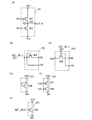
図11(A)に示す単極性回路は一例として特許文献1の図1に記載のシフトレジスタを構成するパルス出力回路の1段目について示した回路であり、トランジスタTr11、トランジスタTr12、トランジスタTr13、トランジスタTr14、トランジスタTr15、トランジスタTr16、容量素子CAを有するものである。また図11(A)中、NAはトランジスタTr12のゲート端子のノード、NBはトランジスタTr13のゲート端子のノード、NCは出力端子のノードについて、示すものである。また図11(A)では、トランジスタTr12に第1のクロック信号CK1が入力され、トランジスタTr14に第2のクロック信号CK2が入力され、トランジスタTr11及びトランジスタTr15にスタートパルスVstが入力され、トランジスタTr13、トランジスタTr15、トランジスタTr16に低電源電位(Vss)が供給される構成が開示されている。また図11(A)で信号GS_(1)は、1段目のパルス出力回路の信号について示すものである。また図11(B)に示すタイミングチャートは、特許文献1の図2に記載の図11(A)に示す回路のタイミングチャートである。図11(A)中の各素子は、図11(B)の信号に応じて動作することとなる。
The unipolar circuit illustrated in FIG. 11A is a circuit illustrated as an example of the first stage of the pulse output circuit included in the shift register illustrated in FIG. 1 of
図11(A)中のノードNAでは、出力信号を高電源電位の信号(H信号ともいう)にするために、定期的に、電気的にフローティング状態(浮遊状態)及び所定の電位が入力される状態がある(図11(B)中、NAで点線の期間がフローティング状態の期間、実線の期間が所定の電位が入力される期間)。同様に、図11(A)中のノードNBでは、出力信号を低電源電位の信号(L信号ともいう)に保持するために、定期的に、電気的にフローティング状態及び所定の電位が入力される状態がある(図11(B)中、NBで点線の期間がフローティング状態の期間、実線の期間が所定の電位が入力される期間)。 At the node NA in FIG. 11A, an electrically floating state (floating state) and a predetermined potential are periodically input in order to make the output signal a high power supply potential signal (also referred to as an H signal). In FIG. 11B, a dotted line period is a floating state at NA, and a solid line period is a period during which a predetermined potential is input. Similarly, in the node NB in FIG. 11A, an electrically floating state and a predetermined potential are periodically input in order to hold the output signal as a low power supply potential signal (also referred to as an L signal). In FIG. 11B, there is a state in which a dotted line period is a floating state in NB and a solid line period is a period during which a predetermined potential is input.
上述したように、チャネル領域が非晶質半導体によって構成される薄膜トランジスタを単極性の駆動回路に用いる場合、しきい値電圧のばらつきを生じることで、トランジスタがエンハンスメント型(ノーマリーオフともいう)、ディプレッション型(ノーマリーオンともいう)になることがある。ノーマリーオンの場合には、ノードNAの電位が、特に図11(B)中、Aの期間で、トランジスタTr16からのリーク電流により低下し、出力信号をH信号に保持できないといった問題がある。同様に、ノーマリーオンの場合には特に図11(B)中、Bの期間で、ノードNBの電位がトランジスタTr15からのリーク電流により低下し、ゲート電位がLレベルであっても、出力信号をL信号に保持できないといった問題がある。また、トランジスタがノーマリーオンとなることを抑制するために、各端子に入力する電位を調整することで対策をとった場合、トランジスタがノーマリーオフとなった場合には所望の動作が得られないといった問題が生じる。 As described above, in the case where a thin film transistor whose channel region is formed using an amorphous semiconductor is used for a unipolar driver circuit, the threshold voltage varies, so that the transistor is an enhancement type (also referred to as normally-off). It may become a depletion type (also called normally-on). In the case of normally-on, there is a problem that the potential of the node NA decreases due to the leakage current from the transistor Tr16 particularly in the period A in FIG. 11B, and the output signal cannot be held as the H signal. Similarly, in the case of normally-on, in particular in the period B in FIG. 11B, even if the potential of the node NB decreases due to the leakage current from the transistor Tr15 and the gate potential is L level, the output signal Is not held in the L signal. In addition, in order to prevent the transistor from being normally on, when a countermeasure is taken by adjusting the potential input to each terminal, the desired operation can be obtained when the transistor is normally off. The problem of not occurring.
なお、図11(A)、(B)に示す例に限らずに、ダイナミック駆動により、順次パルスを出力する駆動回路の場合には、リーク電流の増加が誤動作の原因になる。また、パルス出力回路を具備する駆動回路を生産する上で、エンハンスメント型、またはディプレッション型となるかが基板毎に異なるといったバラツキが生じることもあり、その際予めエンハンスメント型、またはディプレッション型の一方となる際の対策を講じた回路設計では、エンハンスメント型、またはディプレッション型の他方となった際の対応が難しくなるといった問題もあり得る。そのため、薄膜トランジスタの特性がエンハンスメント型、またはディプレッション型であるに関わらず、誤動作のない駆動回路となる回路設計であることが求められる。 Note that, in addition to the examples shown in FIGS. 11A and 11B, in the case of a driving circuit that sequentially outputs pulses by dynamic driving, an increase in leakage current causes malfunction. In addition, when producing a drive circuit having a pulse output circuit, there may be variations such as whether the enhancement type or the depletion type differs depending on the substrate. In this case, either the enhancement type or the depletion type is previously determined. In the circuit design that takes measures when it becomes, there may be a problem that it becomes difficult to cope with the other of the enhancement type or the depression type. Therefore, it is required that the circuit design be a drive circuit that does not malfunction, regardless of whether the characteristics of the thin film transistor are an enhancement type or a depletion type.
そこで本発明の一態様は、チャネルが非晶質半導体によって構成される薄膜トランジスタを単極性の駆動回路に用いる際、薄膜トランジスタの作製条件等に起因するしきい値電圧のばらつきによって、エンハンスメント型、またはディプレッション型のいずれかに変動する駆動回路であっても、回路内の誤動作を低減できる駆動回路を提供することを課題の一とする。 Thus, according to one embodiment of the present invention, when a thin film transistor whose channel is formed using an amorphous semiconductor is used for a unipolar driver circuit, an enhancement type or a depletion mode depends on variations in threshold voltage caused by thin film transistor manufacturing conditions and the like. An object is to provide a driver circuit that can reduce malfunctions in a circuit even if the driver circuit varies in any of the types.
本発明の一態様は、複数段のパルス出力回路を有する駆動回路において、パルス出力回路は、第1のノード、第2のノードの電位に応じて出力信号を出力するための第1の回路と、第1のノードに、前段のパルス出力回路の出力信号に応じた信号を供給する第2の回路と、第2のノードに間欠的に高電源電位の信号を供給するための第3の回路と、第2のノードがゲートに電気的に接続され、第2のノードの電位に応じて、第1のノードの電位を制御するための第1のトランジスタと、前段のパルス出力回路の出力信号に応じた信号がゲートに供給され、第2のノードの電位を制御するための第2のトランジスタと、を有し、第1のトランジスタ及び第2のトランジスタのソース端子と、低電源電位を供給する配線との間には、ソース端子の電位を低電源電位より昇圧するための第4の回路が設けられており、ソース端子の電位を低電源電位にするためのスイッチを有し、スイッチは、第1のトランジスタ及び第2のトランジスタがエンハンスメント型、またはディプレッション型であるかを判定する判定回路によって、制御されることを特徴とする駆動回路である。 According to one embodiment of the present invention, in a driver circuit including a plurality of stages of pulse output circuits, the pulse output circuit includes a first circuit for outputting an output signal in accordance with potentials of the first node and the second node; A second circuit for supplying a signal corresponding to the output signal of the preceding pulse output circuit to the first node, and a third circuit for intermittently supplying a signal of a high power supply potential to the second node A second node electrically connected to the gate, a first transistor for controlling the potential of the first node in accordance with the potential of the second node, and an output signal of the preceding pulse output circuit And a second transistor for controlling the potential of the second node, and a low power supply potential is supplied to the source terminal of the first transistor and the second transistor. Between the source wiring and the source terminal A fourth circuit for boosting the power supply potential from the low power supply potential, and has a switch for setting the potential of the source terminal to the low power supply potential. The switch includes the first transistor and the second transistor. The driving circuit is controlled by a determination circuit that determines whether it is an enhancement type or a depletion type.
本発明の一態様において、第4の回路は、ゲートとドレイン端子が電気的に接続され、ソース端子が低電源電位が供給される配線に電気的に接続されたトランジスタを有する回路である駆動回路でもよい。 In one embodiment of the present invention, the fourth circuit is a circuit including a transistor in which a gate and a drain terminal are electrically connected and a source terminal is electrically connected to a wiring to which a low power supply potential is supplied. But you can.
本発明の一態様において、第4の回路を構成するトランジスタのL/Wは、第1のトランジスタ及び第2のトランジスタのL/Wより大きい駆動回路でもよい。 In one embodiment of the present invention, a driver circuit in which L / W of a transistor included in the fourth circuit is larger than L / W of the first transistor and the second transistor may be used.
本発明の一態様において、判定回路は、定電流源、トランジスタ、コンパレータ、及びバッファ回路を有する駆動回路でもよい。 In one embodiment of the present invention, the determination circuit may be a driver circuit including a constant current source, a transistor, a comparator, and a buffer circuit.
本発明の一態様において、スイッチはトランジスタである駆動回路でもよい。 In one embodiment of the present invention, the switch may be a driver circuit that is a transistor.
本発明の一態様において、駆動回路を構成するトランジスタは、酸化物半導体層でなる半導体層を有する駆動回路でもよい。 In one embodiment of the present invention, the transistor included in the driver circuit may be a driver circuit including a semiconductor layer formed using an oxide semiconductor layer.
本発明の一態様により、チャネルが非晶質半導体によって構成される薄膜トランジスタを単極性の駆動回路に用いる際、薄膜トランジスタの作製条件等に起因するしきい値電圧のばらつきによって、エンハンスメント型、またはディプレッション型のいずれかに変動する駆動回路であっても、回路内の誤動作を低減できる駆動回路を提供することができる。 According to one embodiment of the present invention, when a thin film transistor whose channel is formed using an amorphous semiconductor is used for a unipolar driver circuit, an enhancement type or a depletion type is used depending on variations in threshold voltage caused by thin film transistor manufacturing conditions and the like. Even if the driving circuit fluctuates to any of the above, it is possible to provide a driving circuit that can reduce malfunctions in the circuit.
以下、本発明の実施の形態について図面を参照しながら説明する。但し、本発明は多くの異なる態様で実施することが可能であり、本発明の趣旨及びその範囲から逸脱することなくその形態及び詳細を様々に変更し得ることは当業者であれば容易に理解される。従って実施の形態の記載内容に限定して解釈されるものではない。なお、以下に説明する本発明の構成において、同じ物を指し示す符号は異なる図面間において共通とする。 Hereinafter, embodiments of the present invention will be described with reference to the drawings. However, the present invention can be implemented in many different modes, and those skilled in the art can easily understand that the modes and details can be variously changed without departing from the spirit and scope of the present invention. Is done. Therefore, the present invention is not construed as being limited to the description of the embodiments. Note that in the structures of the present invention described below, the same reference numeral is used in different drawings.
なお、各実施の形態の図面等において示す各構成の、大きさ、層の厚さ、又は領域は、明瞭化のために誇張されて表記している場合がある。よって、必ずしもそのスケールに限定されない。 Note that the size, the layer thickness, or the region of each structure illustrated in the drawings and the like in the embodiments is exaggerated for simplicity in some cases. Therefore, it is not necessarily limited to the scale.
なお本明細書にて用いる第1、第2、第3、乃至第N(Nは自然数)という用語は、構成要素の混同を避けるために付したものであり、数的に限定するものではないことを付記する。 Note that the terms “first”, “second”, “third” to “N” (N is a natural number) used in this specification are given to avoid confusion of components and are not limited numerically. I will add that.
(実施の形態1)
本実施の形態では、まず、複数段のパルス出力回路を有する駆動回路でのパルス出力回路の一段の構成について図面を参照して説明する。
(Embodiment 1)
In this embodiment, first, a structure of one stage of a pulse output circuit in a driving circuit having a plurality of stages of pulse output circuits will be described with reference to the drawings.
本実施の形態で示すパルス出力回路100は、第1の回路101、第2の回路102、第3の回路103、第4の回路104A及び104B、第1のトランジスタ105、第2のトランジスタ106、スイッチ107A及び107Bを有する。なおパルス出力回路100を構成する各トランジスタはnチャネル型の薄膜トランジスタである。
A
なおパルス出力回路100を構成する各トランジスタの半導体層として、酸化物半導体を用いてもよい。酸化物半導体を用いたトランジスタはアモルファスシリコン等のシリコン系半導体材料を用いたトランジスタと比較して電界効果移動度が高い。なお酸化物半導体としては、例えば、酸化亜鉛(ZnO)、酸化スズ(SnO2)なども用いることができる。また、ZnOにInやGaなどを添加することもできる。
Note that an oxide semiconductor may be used as a semiconductor layer of each transistor included in the
酸化物半導体としてInMO3(ZnO)x(x>0)で表記される薄膜を用いることができる。なお、Mは、ガリウム(Ga)、鉄(Fe)、ニッケル(Ni)、マンガン(Mn)及びコバルト(Co)から選ばれた一の金属元素又は複数の金属元素を示す。例えばMとして、Gaの場合があることの他、GaとNi又はGaとFeなど、Ga以外の上記金属元素が含まれる場合がある。また、上記酸化物半導体において、Mとして含まれる金属元素の他に、不純物元素としてFe、Niその他の遷移金属元素、又は該遷移金属の酸化物が含まれているものがある。例えば、酸化物半導体層としてIn−Ga−Zn−O系膜を用いることができる。 As the oxide semiconductor, a thin film represented by InMO 3 (ZnO) x (x> 0) can be used. Note that M represents one metal element or a plurality of metal elements selected from gallium (Ga), iron (Fe), nickel (Ni), manganese (Mn), and cobalt (Co). For example, M may be Ga, and may contain the above metal elements other than Ga, such as Ga and Ni or Ga and Fe. In addition to the metal element contained as M, some of the above oxide semiconductors contain Fe, Ni, other transition metal elements, or oxides of the transition metal as impurity elements. For example, an In—Ga—Zn—O-based film can be used as the oxide semiconductor layer.
酸化物半導体(InMO3(ZnO)x(x>0)膜)としてIn−Ga−Zn−O系膜のかわりに、Mを他の金属元素とするInMO3(ZnO)x(x>0)膜を用いてもよい。また、酸化物半導体として上記の他にも、In−Sn−Zn−O系、In−Al−Zn−O系、Sn−Ga−Zn−O系、Al−Ga−Zn−O系、Sn−Al−Zn−O系、In−Zn−O系、Sn−Zn−O系、Al−Zn−O系、In−O系、Sn−O系、Zn−O系の酸化物半導体を適用することができる。 Oxide semiconductor (InMO 3 (ZnO) x ( x> 0) layer) in place of the In-Ga-ZnO-based film as, InMO 3 for the M and another metal element (ZnO) x (x> 0 ) A membrane may be used. In addition to the above oxide semiconductors, In—Sn—Zn—O-based, In—Al—Zn—O-based, Sn—Ga—Zn—O-based, Al—Ga—Zn—O-based, Sn— Applying an Al-Zn-O-based, In-Zn-O-based, Sn-Zn-O-based, Al-Zn-O-based, In-O-based, Sn-O-based, or Zn-O-based oxide semiconductor is used. Can do.
なお、第1の回路101は、第1のノードNA、第2のノードNBの電位に応じて高電源電位の信号または低電源電位の信号を出力信号として出力するための回路であり、第1のノードNA、第2のノードNBの電位に応じて当該段(図1ではN段目)の出力信号OUT_(N)とする回路である。
Note that the
なお高電源電位とは、基準電位より高い電位のことであり、低電源電位とは基準電位以下の電位のことをいう。なお高電源電位及び低電源電位ともに、トランジスタが動作できる程度の電位、すなわち高電源電位がゲートに印加されることで理想的なトランジスタ(しきい値電圧が0V)がオン状態となり、低電源電位が印加されることで理想的なトランジスタオフ状態となる電位であることが望ましい。 Note that a high power supply potential is a potential higher than a reference potential, and a low power supply potential is a potential lower than the reference potential. Note that both the high power supply potential and the low power supply potential are applied to the gate so that the transistor can operate, that is, the ideal transistor (threshold voltage is 0 V) is turned on, and the low power supply potential is low. It is desirable that the potential be an ideal transistor off state when is applied.
なお、電圧とは、ある電位と、基準の電位(例えばグラウンド電位)との電位差のことを示す場合が多い。よって、電圧、電位、電位差を、各々、電位、電圧、電圧差と言い換えることが可能である。 Note that the voltage often indicates a potential difference between a certain potential and a reference potential (for example, a ground potential). Thus, voltage, potential, and potential difference can be referred to as potential, voltage, and voltage difference, respectively.
なお、薄膜トランジスタの構成は、様々な形態をとることができ、特定の構成に限定されない。例えば、ゲート電極が2個以上のマルチゲート構造を適用することができる。 Note that the structure of the thin film transistor can take various forms and is not limited to a specific structure. For example, a multi-gate structure having two or more gate electrodes can be applied.
また、チャネル領域の上下にゲート電極が配置されている構造を適用することができる。なお、チャネル領域の上下にゲート電極が配置される構成にすることにより、複数の薄膜トランジスタが並列に接続されたような構成とすることも可能である。 A structure in which gate electrodes are provided above and below a channel region can be used. Note that a structure in which a plurality of thin film transistors are connected in parallel is also possible by using a structure in which gate electrodes are provided above and below a channel region.
なお、AとBとが接続されている、と明示的に記載する場合は、AとBとが電気的に接続されている場合と、AとBとが機能的に接続されている場合と、AとBとが直接接続されている場合とを含むものとする。ここで、A、Bは、対象物(例えば、装置、素子、回路、配線、電極、端子、導電膜、層、など)であるとする。したがって、所定の接続関係、例えば、図または文章に示された接続関係に限定されず、図または文章に示された接続関係以外のものも含むものとする。 In addition, when it is explicitly described that A and B are connected, A and B are electrically connected, and A and B are functionally connected. , A and B are directly connected. Here, A and B are objects (for example, devices, elements, circuits, wirings, electrodes, terminals, conductive films, layers, etc.). Therefore, it is not limited to a predetermined connection relationship, for example, the connection relationship shown in the figure or text, and includes things other than the connection relation shown in the figure or text.
なお第1のノードNAとは、第1の回路101、第2の回路102、及び第1のトランジスタ105に接続されるノードであり、第2のノードNBとは、第1の回路101、第3の回路103、第1のトランジスタ105、第2のトランジスタ106に接続されるノードである。
Note that the first node NA is a node connected to the
第2の回路102は、第1のノードNAに、前段のパルス出力回路の出力信号OUT_(N−1)(1段目であれば、スタートパルスSP)に応じた信号を供給するための回路である。また第2の回路102は、前段のパルス出力回路の出力信号OUT_(N−1)を、第2のトランジスタ106のゲートに出力するための回路である。
The
第3の回路103は、第2のノードNBに対し、クロック信号の入力等によって得られる所定のタイミングに応じて、間欠的に高電源電位の信号を供給するための回路である。
The
第1のトランジスタ105は、第2のノードNBがゲートに接続され、ドレイン端子が第1のノードNAに接続され、第2のノードNBの電位に応じて、第1のノードNAの電位を制御するためのトランジスタである。
In the
第2のトランジスタ106は、前段のパルス出力回路の出力信号OUT_(N−1)に応じた信号がゲートに供給され、ドレイン端子が第2のノードNBに接続され、第2のノードNBの電位を制御するためのトランジスタである。
In the
なお、薄膜トランジスタは、ゲート端子と、ドレイン端子と、ソース端子とを含む少なくとも三つの端子を有する素子であり、ドレイン領域とソース領域の間にチャネル領域を有しており、ドレイン領域とチャネル領域とソース領域とを介して電流を流すことが出来る。本明細書においては、高電源電位を供給するための配線側に接続される端子をドレイン端子、低電源電位が供給される配線側に接続される端子をソース端子として説明することとする。なお、ソース端子とドレイン端子を、第1端子、第2端子と表記する場合がある。 Note that a thin film transistor is an element having at least three terminals including a gate terminal, a drain terminal, and a source terminal, and has a channel region between the drain region and the source region. Current can flow through the source region. In this specification, a terminal connected to the wiring side for supplying a high power supply potential is described as a drain terminal, and a terminal connected to the wiring side to which a low power supply potential is supplied is described as a source terminal. Note that the source terminal and the drain terminal may be referred to as a first terminal and a second terminal.
第4の回路104Aは、第1のトランジスタ105のソース端子と、低電源電位を供給する配線110との間に設け、第1のトランジスタ105のソース端子の電位を配線110の電位より昇圧させる回路である。また第4の回路104Bは、第4の回路104Aと同様に、第2のトランジスタ106のソース端子と、低電源電位を供給する配線110との間に設け、第2のトランジスタ106のソース端子の電位を配線110の電位より昇圧させる回路である。
The
なお本実施の形態で示す構成において、第4の回路104Aとして第3のトランジスタ108A、第4のトランジスタ109Aを設け、それぞれのトランジスタのゲートとドレイン端子を短絡するように接続している。その結果、第1のトランジスタ105のソース端子、すなわち第3のノードN1の電位を配線110の電位より第3のトランジスタ108Aと第4のトランジスタ109Aとのしきい値電圧の和の分だけ高くすることができる。同様に、第4の回路104Bとして第3のトランジスタ108B、第4のトランジスタ109Bを設け、それぞれのトランジスタのゲートとドレイン端子を短絡するように接続している。その結果、第2のトランジスタ106のソース端子、すなわち第3のノードN2の電位を配線110の電位より第3のトランジスタ108Bと第4のトランジスタ109Bとのしきい値電圧の和の分だけ高くすることができる。なお第4の回路104A及び第4の回路104Bは、いずれか一方を省略してもよいし、さらに複数のトランジスタで冗長化してもよい。
Note that in the structure described in this embodiment, a third transistor 108A and a
なお、第4の回路104A及び第1のトランジスタ105、並びに第4の回路104B及び第2のトランジスタ106は、第1の回路101を制御するためにフローティング状態とするノードの数に応じて設けられるものである。本実施の形態では一例として、第1のノードNA及び第2のノードNBの2つの構成を示すものである。また本実施の形態では、第4の回路104Aとして第3のトランジスタ108A及び第4のトランジスタ109Aの2つ、並びに第4の回路104Bとして第3のトランジスタ108B及び第4のトランジスタ109Bの2つを配置する構成としたが、更にトランジスタ数を増やして、第3のノードN1、N2の電位を高くするようにする構成としてもよい。また、第4の回路104A、104Bを構成するトランジスタである第3のトランジスタ108A、第4のトランジスタ109A、及び第3のトランジスタ108B、第4のトランジスタ109Bのトランジスタの抵抗値を、さらなるオフ電流の低減のために、第1のトランジスタ105、第2のトランジスタ106よりも高くなるように予めすることが好ましい。
Note that the
すなわち第4の回路を構成するトランジスタである第3のトランジスタ108A、第4のトランジスタ109A、及び第3のトランジスタ108B、第4のトランジスタ109BのトランジスタのL/W比を、第1のトランジスタ105、第2のトランジスタ106のL/W比より大きくすることが好ましい。また、第4の回路を構成するトランジスタである第3のトランジスタ108A、第4のトランジスタ109A、及び第3のトランジスタ108B、第4のトランジスタ109Bの半導体層の膜厚を、第1のトランジスタ105、第2のトランジスタ106の半導体層の膜厚より小さくすることが好ましい。なおゲート長Lはトランジスタのゲートと半導体層が重なる領域でのソース、ドレイン間の長さに相当し、ゲート幅Wはトランジスタのゲートと半導体層が重なる領域でのソース、ドレイン間の幅に相当する。従って、L/W比は、ゲート長とゲート幅の比に相当する。
That is, the L / W ratio of the transistors of the third transistor 108A, the
スイッチ107Aは、第1のトランジスタ105のソース端子、すなわち第3のノードN1を低電源電位が供給される配線110と短絡するための回路である。スイッチ107Bは、第1のトランジスタ105のソース端子及び第2のトランジスタ106のソース端子、すなわち第3のノードN2を低電源電位が供給される配線110と短絡するための回路である。なおスイッチ107A、107Bとしては、第1乃至第4のトランジスタと同様に作製されるトランジスタで形成すればよい。また、スイッチ107A、107Bのオンまたはオフは、外部に設けられた判定回路111により供給される判定信号により制御される。なおスイッチ107A、107Bをトランジスタで作製する場合には、判定回路111からの信号は当該トランジスタを確実にオン又はオフできる電位の信号であることが好ましい。なお、スイッチ107A、Bと同様の機能を有するスイッチをさらに複数設ける構成としてもよい。
The
すなわち第1のトランジスタ105及び第2のトランジスタ106がノーマリーオンの場合には、第4の回路104A、104Bにより第3のノードN1、N2を低電源電位Vssより高くして、第1のトランジスタ105及び第2のトランジスタ106を電流が流れにくくし、ノーマリーオフのときにはスイッチ107A、107Bを短絡させて第3のノードN1、N2の電位を低電源電位に下げることで第1のトランジスタ105及び第2のトランジスタ106を電流が流れやすくし、ノーマリーオンでもノーマリーオフでも問題なく動作させることができるものとなる。なお、スイッチ107A、107Bをトランジスタで構成する場合には、ノーマリーオンであると動作が不安定になるので、外部回路である判定回路111よりスイッチ107A、107Bとなるトランジスタのゲートに十分な電圧レベルの信号を印加する構成とすることが好ましい。
That is, when the
次いで判定回路111の構成例について図2を用いて説明する。
Next, a configuration example of the
判定回路111は、定電流源201、トランジスタ202、コンパレータ203(比較回路ともいう)、バッファ回路204を有する。なお、定電流源201と、トランジスタ202、及びコンパレータ203が接続されるノードを、説明のため、ノードNEと呼ぶことにする。
The
図2において、定電流源201は一方の端子が高電源電位Vddを供給する配線に接続され、他方の端子がノードNEに接続される。トランジスタ202はドレイン端子がノードNEに接続され、ゲート及びソース端子が低電源電位Vssを供給する配線に接続される。コンパレータ203は、入力端子がノードNEに接続され、出力端子がバッファ回路204の入力端子に接続される。バッファ回路204の出力端子は、スイッチ107A、1070Bとなるトランジスタのゲートに接続される。
In FIG. 2, the constant
なお、バッファ回路204は、トランジスタでなるスイッチ107A、107Bまでの距離が長い場合に、各段のパルス出力回路に入力するための信号の電荷供給能力を高めるために設けるものであり、省略してもよい。
Note that the
判定回路111ではトランジスタ202が、駆動回路を構成するトランジスタのノーマリーオンまたはノーマリーオフを判定するためのトランジスタであり、同一基板上に同じ条件で作製され、同じトランジスタ特性を有するものである。そして定電流源201より流れる電流がトランジスタ202を流れる際、トランジスタ202がノーマリーオンまたはノーマリーオフによって、ノードNEの電位の高低を判定することで、スイッチ107A、107Bのオン又はオフを制御するものである。なお、トランジスタ202がノーマリーオンとなるときには、トランジスタ202がノーマリーオフとなるときより、ノードNEの電位が低くなる。なおコンパレータ203では予め設定された参照電位(一例としては、高電源電位Vddと低電源電位Vssとの中間電位)とノードNEの電位を比較し、ノーマリーオフのときには、高電源電位の信号を出力し、ノーマリーオンのときには低電源電位の信号を出力する。そしてバッファ回路204で、トランジスタでなるスイッチ107A、107Bのオン又はオフを十分制御できる電圧の信号(判定信号)となる。
In the
なお、駆動回路を構成するトランジスタがノーマリーオンであるかノーマリーオフであるかは、作製工程が同じであっても基板毎にばらつきが生じることもあり得る。そのため、本実施の形態の構成によって、ノーマリーオンであるかノーマリーオフであるかを表示装置となる基板毎に判定し、補正することのできる構成により、駆動回路での歩留まりの向上を図ることができる。 Note that whether a transistor included in the driver circuit is normally on or normally off may vary from substrate to substrate even in the same manufacturing process. Therefore, with the configuration of this embodiment, it is possible to determine for each substrate that is a display device whether the device is normally on or normally off, and to correct the driving circuit, thereby improving the yield in the driving circuit. be able to.
なおコンパレータ203で比較する参照電位は、ノーマリーオンとなる際のノードNEの電位の上昇、及びノーマリーオフとなる際のノードNEの電位の低下を予めモニターしておき、適宜設定される電位であってもよい。
Note that the reference potential to be compared by the
次いで、第1の回路101、第2の回路102、及び第3の回路103の一例について、図3を用いて説明する。
Next, examples of the
図3(A)に示す第1の回路101の一例としては、図11(A)と同様に、トランジスタ301、トランジスタ302を設ける。そしてトランジスタ301のゲートを第1のノードNAに接続し、トランジスタ302のゲートを第2のノードNBに接続し、トランジスタ301のドレイン端子をクロック信号CK1(第1のクロック信号ともいう)が供給される配線に接続し、トランジスタ301のソース端子とトランジスタ302のドレイン端子とを接続して出力信号OUT_Nを出力する端子とし、トランジスタ302のソース端子を低電源電位Vssを供給する配線に接続する構成とすればよい。また、トランジスタ301のゲートとソースの間に必要に応じて、容量素子303を設ける構成としてもよい。容量素子を設けることで、第1のノードがフローティング状態となった際に、ゲートとソースの間でのブートストラップが起こりやすくなり好適である。
As an example of the
次いで図3(B)に示す第2の回路102の一例としては、図11(A)と同様に、トランジスタ304を設ける。そして、トランジスタ304のゲートとドレイン端子、及び第2のトランジスタ106のゲートが接続される端子を前段のパルス出力回路の出力信号OUT_(N−1)が入力される端子に接続し、トランジスタ304のソース端子を第2のノードNBに接続する構成とすればよい。また図3(B)とは異なる第2の回路102の別の構成としては、図3(C)に示すトランジスタ305を設ける構成がある。そして、トランジスタ305のドレイン端子を高電源電位Vddが供給される配線に接続し、トランジスタ305のゲート及び第2のトランジスタ106のゲートが接続される端子を前段のパルス出力回路の出力信号OUT_(N−1)が入力される端子に接続し、トランジスタ305のソース端子を第2のノードNBに接続する構成とすればよい。
Next, as an example of the
次いで図3(D)に示す第3の回路103の一例としては、図11(A)と同様に、トランジスタ306を設ける。トランジスタ306のゲート及びドレイン端子をクロック信号CK2(第2のクロック信号ともいう)が供給される配線に接続し、トランジスタ306のソース端子を第2のノードNBに接続する構成とする。なお図3(D)でのクロック信号CK2は、図3(A)でのクロック信号CK1の反転信号であることが好ましい。また図3(D)とは異なる第3の回路103の別の構成としては、図3(E)に示すトランジスタ307及びトランジスタ308がある。トランジスタ307のゲートをクロック信号CK2(第2のクロック信号ともいう)が供給される配線に接続し、トランジスタ307のドレイン端子を高電源電位Vddが供給される配線に接続し、トランジスタ307のソース端子とトランジスタ308のドレイン端子とを接続し、トランジスタ308のゲートをクロック信号CK3(第3のクロック信号ともいう)が供給される配線に接続され、トランジスタ308のソース端子が第2のノードNBに接続される構成とする。なお、図3(D)でのクロック信号CK2は、図3(A)でのクロック信号CK1が1/4周期分遅延した信号であり、図3(E)でのクロック信号CK3は、図3(E)でのクロック信号CK2が1/4周期分遅延した信号であることが好ましい。
Next, as an example of the
また図1に示す構成は、第1の回路101、第2の回路102、及び第3の回路103の他にも、別途回路を設ける構成としてもよい。例えば、図3(F)に示すトランジスタ309を有する回路を図1に示す第2のノードNBに接続して設ける。図3(F)に示すトランジスタ309は、ドレイン端子を高電源電位Vddが供給される端子に接続し、ゲートをパルス出力回路で2段後段の出力信号OUT_(N+2)が入力される端子に接続し、ソース端子を第2のノードNBに接続する構成とすればよい。図3(F)に示す回路を追加して設ける構成とすることで第2のノードNBの電位をより確実に制御することが出来るため好適である。
In addition to the
なお第1の回路101、第2の回路102、及び第3の回路103をそれぞれ複数個設ける構成とすることも可能である。
Note that a plurality of
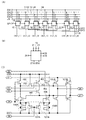
次いで、複数段のパルス出力回路を具備する駆動回路であるシフトレジスタの構成について図4に示し、本実施形態で示す構成の効果等について詳述していく。なお、図4は、図1における第1の回路101として図3(A)の回路とし、図1における第2の回路102として図3(C)の回路とし、図1における第3の回路103として図3(E)の回路とし、第2のノードNBに図3(F)の回路を設ける構成について具体的に示した回路である。なお図4では第1の回路101を複数設ける例について説明するものである。
Next, the structure of a shift register, which is a driving circuit including a plurality of stages of pulse output circuits, is shown in FIG. 4, and effects of the structure shown in this embodiment will be described in detail. 4 is the circuit of FIG. 3A as the
図4(A)に示すシフトレジスタは、第1のパルス出力回路10_1乃至第Nのパルス出力回路10_N(N≧3の自然数)を有している。図4(A)に示すシフトレジスタの第1のパルス出力回路10_1乃至第Nのパルス出力回路10_Nには、第1の配線11より第1のクロック信号CK1、第2の配線12より第2のクロック信号CK2、第3の配線13より第3のクロック信号CK3、第4の配線14より第4のクロック信号CK4が供給される。また第1のパルス出力回路10_1では、第5の配線15からのスタートパルスSP1(第1のスタートパルス)が入力される。また2段目以降の第nのパルス出力回路10_n(nは、2≦n≦Nの自然数)では、一段前段のパルス出力回路からの信号(前段信号OUT(n−1)という)が入力される。また第1のパルス出力回路10_1では、2段後段の第3のパルス出力回路10_3からの信号が入力される。同様に、2段目以降の第nのパルス出力回路10_nでは、2段後段の第(n+2)のパルス出力回路10_(n+2)からの信号(後段信号OUT(n+2)という)が入力される。従って、各段のパルス出力回路からは、後段及び/または二つ前段のパルス出力回路に入力するための第1の出力信号OUT(1)(SR)〜OUT(N)(SR)、別の回路等に入力される第2の出力信号OUT(1)〜OUT(N)が出力される。また各段のパルス出力回路には、第6の配線16より、判定回路111からの判定信号JSが供給される。ただし、図4(A)に示すように、シフトレジスタの最終段の2つの段には、後段信号OUT(n+2)が入力されないため、一例としては、別途第7の配線17より第2のスタートパルスSP2、第8の配線18より第3のスタートパルスSP3をそれぞれ入力する構成でもよい。または別途、内部で生成された信号であってもよい。例えば、表示部へのパルス出力に寄与しない第(n+1)のパルス出力回路10(n+1)、第(n+2)のパルス出力回路10(n+2)を設け(ダミー段ともいう)、当該ダミー段より第2のスタートパルス(SP2)及び第3のスタートパルス(SP3)に相当する信号を生成する構成としてもよい。
The shift register illustrated in FIG. 4A includes the first pulse output circuit 10_1 to the Nth pulse output circuit 10_N (N ≧ 3 is a natural number). In the first pulse output circuit 10_1 to the Nth pulse output circuit 10_N of the shift register illustrated in FIG. 4A, the first clock signal CK1 from the first wiring 11 and the second clock output from the second wiring 12 are second. The third clock signal CK3 is supplied from the clock signal CK2, the
なお、第1のクロック信号(CK1)〜第4のクロック信号(CK4)は、一定の間隔でH信号とL信号を繰り返す信号である。また、第1のクロック信号(CK1)〜第4のクロック信号(CK4)は、順に1/4周期分遅延している(すなわち、互いに90°位相がずれている)。本実施の形態では、第1のクロック信号(CK1)〜第4のクロック信号(CK4)を利用して、パルス出力回路の駆動の制御等を行う。なお、クロック信号は、入力される駆動回路に応じて、GCK、SCKということもあるが、ここではCKとして説明を行う。 Note that the first clock signal (CK1) to the fourth clock signal (CK4) are signals that repeat the H signal and the L signal at regular intervals. Further, the first clock signal (CK1) to the fourth clock signal (CK4) are sequentially delayed by a quarter period (that is, 90 ° out of phase with each other). In this embodiment, driving of the pulse output circuit is controlled by using the first clock signal (CK1) to the fourth clock signal (CK4). Note that although the clock signal is sometimes referred to as GCK or SCK depending on the input driving circuit, it is described here as CK.
第1のパルス出力回路10_1〜第Nのパルス出力回路10_Nの各々は、第1の入力端子21、第2の入力端子22、第3の入力端子23、第4の入力端子24、第5の入力端子25、第1の出力端子26、第2の出力端子27、第6の入力端子28を有している(図4(B)参照)。
Each of the first pulse output circuit 10_1 to the Nth pulse output circuit 10_N includes a
図4(B)に図4(A)で示したパルス出力回路10_nの一つを示す。第1の入力端子21、第2の入力端子22及び第3の入力端子23は、第1の配線11〜第4の配線14のいずれかと電気的に接続されている。例えば、図4(A)、(B)において、第1のパルス出力回路10_1は、第1の入力端子21が第1の配線11と電気的に接続され、第2の入力端子22が第2の配線12と電気的に接続され、第3の入力端子23が第3の配線13と電気的に接続されている。また、第2のパルス出力回路10_2は、第1の入力端子21が第2の配線12と電気的に接続され、第2の入力端子22が第3の配線13と電気的に接続され、第3の入力端子23が第4の配線14と電気的に接続されている。
FIG. 4B illustrates one of the
また図4(A)、(B)において、第1のパルス出力回路10_1は、第4の入力端子24にスタートパルスが入力され、第5の入力端子25に後段信号OUT(3)が入力され、第1の出力端子26より第1の出力信号OUT(1)(SR)が出力され、第2の出力端子27より第2の出力信号OUT(1)が出力され、第6の入力端子28より判定信号JSが入力されていることとなる。
4A and 4B, in the first pulse output circuit 10_1, the start pulse is input to the
次に、パルス出力回路の具体的な回路構成の一例について、図4(C)で説明する。 Next, an example of a specific circuit configuration of the pulse output circuit is described with reference to FIG.
第1のパルス出力回路10_1は、図1と同様に、第1の回路101A及び101B、第2の回路102、第3の回路103、第4の回路104A及び104B、第1のトランジスタ105、第2のトランジスタ106、トランジスタでなるスイッチ107A及び107Bを有している。また、図1の構成に加えて第2のノードNBに接続されるトランジスタ401を有する。トランジスタ401は後段信号OUT(n+2)がH信号となるタイミングに応じて、第2のノードNBの電位を上昇させるためのトランジスタである。また、図1の構成に加えて第1のノードNAにおいて、トランジスタ402を挿入し、ゲートを高電源電位Vddが供給される配線に接続する構成としてもよい。トランジスタ402を第1のノードNAに挿入する構成とすることによって、第1の回路101Aでのトランジスタのゲートが、フローティング状態となりやすくなるため好適である。ここで第1のクロック信号(CK1)〜第4のクロック信号(CK4)は、一定の間隔でHレベルとLレベルを繰り返す信号であるが、HレベルのときVdd、LレベルのときVssであるとする。
As in FIG. 1, the first pulse output circuit 10_1 includes the
図4(C)におけるパルス出力回路が第1のパルス出力回路10_1の場合、第1の入力端子21には第1のクロック信号CK1が入力され、第2の入力端子22には第2のクロック信号CK2が入力され、第3の入力端子23には第3のクロック信号CK3が入力され、第4の入力端子24にはスタートパルスSPが入力され、第5の入力端子25には後段信号OUT(3)が入力され、第1の出力端子26からは第1の出力信号OUT(1)(SR)が出力され、第2の出力端子27からは第2の出力信号OUT(1)が出力され、第6の入力端子28からは判定信号JSが入力される。
When the pulse output circuit in FIG. 4C is the first pulse output circuit 10_1, the first clock signal CK1 is input to the
ここで、図4(C)に示したパルス出力回路を複数具備するシフトレジスタのタイミングチャートについて図5に示す。なおシフトレジスタが走査線駆動回路である場合、図5中の期間501は垂直帰線期間であり、期間502はゲート選択期間に相当する。
Here, FIG. 5 shows a timing chart of a shift register including a plurality of pulse output circuits shown in FIG. Note that in the case where the shift register is a scan line driver circuit, a
図4(C)中のノードNAでは、出力信号OUT_(N)をH信号にするために、定期的に、電気的にフローティング状態(浮遊状態)及び所定の電位が入力される状態がある。図5中のNAで矢印A区間の期間がフローティング状態の期間であり、フローティング状態となる際にリーク電流による電位の低下が問題となる期間である。同様に、図5中のノードNBで矢印B区間の期間がフローティング状態の期間であり、フローティング状態となる際にリーク電流による電位の低下が問題となる期間である。具体的にいえば、フローティング状態となる矢印A区間、及び矢印B区間での電位低下の度合いが、トランジスタがノーマリーオンまたはノーマリーオフかによって変化することが問題である。一方で、単にノーマリーオンまたはノーマリーオフの状態を補正する回路を付加するだけでは、ノーマリーオンまたはノーマリーオフの各状態が基板間でばらつく場合に、対策として不十分である。 At the node NA in FIG. 4C, there are a state in which an electrically floating state (floating state) and a predetermined potential are periodically input in order to change the output signal OUT_ (N) to an H signal. A period indicated by an arrow A in FIG. 5 is a period in a floating state, and is a period in which a decrease in potential due to a leakage current becomes a problem when the floating state is entered. Similarly, a period of an arrow B in the node NB in FIG. 5 is a floating period, and a potential drop due to a leakage current becomes a problem when the floating state is entered. More specifically, the problem is that the degree of potential decrease in the arrow A section and the arrow B section in the floating state changes depending on whether the transistor is normally on or normally off. On the other hand, simply adding a circuit that corrects a normally-on or normally-off state is not sufficient as a countermeasure when the normally-on or normally-off state varies between substrates.
次に、図6に図1で示したパルス出力回路の動作について説明する。そしてノーマリーオンまたはノーマリーオフの各状態が基板間でばらつく場合に、いずれの状態であっても正確な動作を補償できる図1のパルス出力回路を具備する駆動回路での動作による効果について説明する。 Next, the operation of the pulse output circuit shown in FIG. 1 will be described with reference to FIG. Then, when each of the normally-on state and the normally-off state varies between the substrates, the effect of the operation in the drive circuit having the pulse output circuit of FIG. 1 capable of compensating for the accurate operation in any state will be described. To do.
まず、判定回路111で各回路を構成するトランジスタがノーマリーオンかノーマリーオフかの指標として、トランジスタ202がノーマリーオンかノーマリーオフの判定を行い、第4の回路104A、104Bによる第3のノードN1、N2の電位の上昇を行うか否かを判定する(図6、ステップ601)。
First, the
次いで、図2に示す判定回路111は、ノードNEの電位が参照電位よりも高いかどうかの判定を行う(図6、ステップ602)。トランジスタ202に流れる電流が大きく、ノードNEの電位が参照電位よりも高くなる場合、トランジスタ202がノーマリーオフであると判定される(図6、ステップ603)。
Next, the
次いで、コンパレータ203及びバッファ回路204を介して判定回路111より、スイッチ107A及び107BにH信号が出力される(図6、ステップ604)。スイッチ107A及び107Bがnチャネル型のトランジスタの場合には、スイッチ107A及び107Bがオン状態となる(図6、ステップ605)。その結果、第3のノードN1、N2の電位が配線110の電位にあたる低電源電位Vssに低下する(図6、ステップ606)。
Next, the H signal is output from the
また逆に、トランジスタ202に流れる電流が小さく、ノードNEの電位が参照電位よりも低くなる場合、トランジスタ202がノーマリーオンであると判定される(図6、ステップ607)。
Conversely, when the current flowing through the
次いで、コンパレータ203及びバッファ回路204を介して判定回路111より、スイッチ107A及び107BにL信号が出力される(図6、ステップ608)。スイッチ107A及び107Bがnチャネル型のトランジスタの場合には、スイッチ107A及び107Bがオフ状態となる(図6、ステップ609)。その結果、第3のノードN1及びN2の電位が低電源電位Vssより高い電位を保持することとなる(図6、ステップ610)。
Next, the L signal is output from the
上述の動作によって第1のトランジスタ105及び第2のトランジスタ106がノーマリーオンであってもノーマリーオフであってもトランジスタがオン状態またはオフ状態をとるのに十分なゲートとソースの間の電圧Vgsを得ることのできるパルス出力回路とすることができる。すなわちノーマリーオンのトランジスタの場合にはトランジスタのゲートとソース端子との間にかかる電圧Vgsを上昇させることで、スイッチング特性の向上を行い、ノーマリーオフのトランジスタの場合にはソース端子の電位を低下させて十分に高い電圧Vgsを確保することができる。そのため、トランジスタがノーマリーオンであるかノーマリーオフであるかが基板毎にばらついても、より確度が高く誤動作を低減することのできる駆動回路とすることができる。すなわち、薄膜トランジスタの作製条件等に起因するしきい値電圧のばらつきによって、エンハンスメント型、またはディプレッション型のいずれかに変動する駆動回路であっても、回路内の誤動作を低減できる駆動回路を提供することができる。
With the above-described operation, a voltage between the gate and the source that is sufficient for the transistor to be on or off regardless of whether the
本実施の形態は、他の実施の形態に記載した構成と適宜組み合わせて実施することが可能である。 This embodiment can be implemented in appropriate combination with the structures described in the other embodiments.
(実施の形態2)
本実施の形態では、上記実施の形態で説明した駆動回路、及び当該駆動回路によって制御される表示部を具備する表示装置の断面図について、図7を用いて説明する。また本実施の形態では、表示装置として液晶表示装置の一例について説明をおこなうが、有機EL素子等の発光素子を具備するEL表示装置、または電気泳動素子を具備する電気泳動表示装置にも適用することが可能である。なお、上記実施の形態で説明した構成は、表示装置の駆動回路に限らず、光センサ用駆動回路等の他の装置にも適用可能である。
(Embodiment 2)
In this embodiment, a cross-sectional view of a display device including the driver circuit described in the above embodiment and a display portion controlled by the driver circuit is described with reference to FIGS. In this embodiment, an example of a liquid crystal display device is described as a display device; however, the present invention is also applied to an EL display device including a light-emitting element such as an organic EL element or an electrophoretic display device including an electrophoretic element. It is possible. Note that the structure described in the above embodiment can be applied not only to the driver circuit of the display device but also to other devices such as an optical sensor driver circuit.
本発明の一形態である液晶表示装置を図7に示す。図7の液晶表示装置は、薄膜トランジスタ701及び容量702を含む画素部、及び薄膜トランジスタ703を含む駆動回路部、画素電極層704、配向膜として機能する絶縁層705が設けられた基板706と、配向膜として機能する絶縁層707、対向電極層708、カラーフィルタとして機能する着色層709が設けられた対向基板710とが液晶層711を挟持して対向している。また、基板706及び対向基板710の液晶層711と反対側には、それぞれ偏光板(偏光子を有する層、単に偏光子ともいう)712a、712bが設けられ、ゲート配線の端子部には第1の端子713、接続電極714、及び接続用の端子電極715、ソース配線の端子部には第2の端子716及び接続用の端子電極717が設けられている。
A liquid crystal display device which is one embodiment of the present invention is shown in FIG. 7 includes a pixel portion including a
駆動回路部において、薄膜トランジスタ703はゲート電極層721及びゲート絶縁層722上の半導体層723の上方の酸化物絶縁層724上に導電層718が設けられ、ドレイン電極層719bはゲート電極層と同工程で形成される導電層720と電気的に接続している。また、画素部において、薄膜トランジスタ701のドレイン電極層は画素電極層704と電気的に接続している。
In the driver circuit portion, the
酸化物半導体を用いた薄膜トランジスタで形成することにより、製造コストを低減することができる。また酸化物半導体を用いた薄膜トランジスタは電界効果移動度が高く表示装置の画素部及び駆動回路を構成するものとして好適である。一方で、酸化物半導体は外因性の不純物が添加されなくても、酸素が抜けた空孔欠陥によりn型化しやすいという性質がある。酸化物半導体層に接して酸化物絶縁膜を形成することによって、安定した電気特性を有する薄膜トランジスタを得ることができるが、仮に酸化物半導体がn型化してノーマリーオンの薄膜トランジスタが形成された場合でも、本実施の形態の駆動回路を用いることによって、駆動回路を安定に動作させることができる。 By forming the thin film transistor using an oxide semiconductor, manufacturing cost can be reduced. A thin film transistor using an oxide semiconductor has high field effect mobility and is suitable for forming a pixel portion and a driver circuit of a display device. On the other hand, an oxide semiconductor has a property of easily becoming n-type due to a vacancy defect from which oxygen has been released, even if an exogenous impurity is not added. A thin film transistor having stable electrical characteristics can be obtained by forming an oxide insulating film in contact with an oxide semiconductor layer. However, a normally-on thin film transistor is formed when the oxide semiconductor is n-type. However, the drive circuit can be stably operated by using the drive circuit of this embodiment.
なお、本実施の形態では、酸化物半導体をチャネルに用いる薄膜トランジスタの例について説明したが、実施の形態1で開示する構成は、駆動回路を構成する薄膜トランジスタがノーマリーオンまたはノーマリーオフでも動作することができるものである。従って、例えば、非晶質シリコンを用いた薄膜トランジスタの半導体層において、意図的または非意図的にn型の導電性を付与する不純物が含まれることによってノーマリーオンとして動作するトランジスタにも、用いることができる。また、チャネル領域を形成する半導体層のゲート絶縁膜とは反対側(バックチャネル側)に電荷が蓄積されることによって寄生チャネルが形成され、ノーマリーオンとして動作するトランジスタにおいても適用可能である。
Note that although an example of a thin film transistor using an oxide semiconductor for a channel is described in this embodiment, the structure disclosed in
半導体層のチャネル形成領域は高抵抗化領域であるので、薄膜トランジスタの電気特性は安定化し、オフ電流の増加などを防止することができる。よって、電気特性が良好で信頼性のよい薄膜トランジスタを有する半導体装置とすることが可能となる。 Since the channel formation region of the semiconductor layer is a high resistance region, the electrical characteristics of the thin film transistor can be stabilized and an increase in off current can be prevented. Therefore, a semiconductor device including a thin film transistor with favorable electric characteristics and high reliability can be obtained.
また、薄膜トランジスタは静電気などにより破壊されやすいため、画素部または駆動回路と同一基板上に保護回路を設けることが好ましい。保護回路は、酸化物半導体層を用いた非線形素子を用いて構成することが好ましい。例えば、保護回路は画素部と、走査線入力端子及び信号線入力端子との間に配設されている。本実施の形態では複数の保護回路を配設して、走査線、信号線及び容量バス線に静電気等によりサージ電圧が印加され、画素トランジスタなどが破壊されないように構成されている。そのため、保護回路にはサージ電圧が印加されたときに、共通配線に電荷を逃がすように構成する。また、保護回路は、走査線に対して並列に配置された非線形素子によって構成されている。非線形素子は、ダイオードのような二端子素子又はトランジスタのような三端子素子で構成される。例えば、画素部の薄膜トランジスタ701と同じ工程で形成することも可能であり、例えばゲート端子とドレイン端子を接続することによりダイオードと同様の特性を持たせることができる。
In addition, since the thin film transistor is easily broken by static electricity or the like, it is preferable to provide a protective circuit over the same substrate as the pixel portion or the driver circuit. The protective circuit is preferably formed using a non-linear element using an oxide semiconductor layer. For example, the protection circuit is provided between the pixel portion and the scanning line input terminal and the signal line input terminal. In this embodiment mode, a plurality of protection circuits are provided so that a surge voltage is applied to the scanning lines, signal lines, and capacitor bus lines due to static electricity or the like, so that the pixel transistors and the like are not destroyed. For this reason, the protection circuit is configured to release charges to the common wiring when a surge voltage is applied. The protection circuit is configured by a non-linear element arranged in parallel to the scanning line. The nonlinear element is configured by a two-terminal element such as a diode or a three-terminal element such as a transistor. For example, it can be formed in the same process as the
本実施の形態は、他の実施の形態に記載した構成と適宜組み合わせて実施することが可能である。 This embodiment can be implemented in appropriate combination with the structures described in the other embodiments.
(実施の形態3)
本実施の形態では、同一基板上に少なくとも駆動回路の一部と、画素部に配置する薄膜トランジスタを作製する例について以下に説明する。なお基板上に配置する薄膜トランジスタは、実施の形態2の断面図に示すよう形成すればよい。
(Embodiment 3)
In this embodiment, an example in which at least part of a driver circuit and a thin film transistor placed in a pixel portion are formed over the same substrate will be described below. Note that the thin film transistor provided over the substrate may be formed as shown in the cross-sectional view of
アクティブマトリクス型表示装置のブロック図の一例を図8(A)に示す。表示装置の基板5300上には、画素部5301、第1の走査線駆動回路5302、第2の走査線駆動回路5303、信号線駆動回路5304、判定回路5306を有する。画素部5301には、複数の信号線が信号線駆動回路5304から延伸して配置され、複数の走査線が第1の走査線駆動回路5302、及び第2の走査線駆動回路5303から延伸して配置されている。なお走査線と信号線との交差領域には、各々、表示素子を有する画素がマトリクス状に配置されている。また、表示装置の基板5300はFPC(Flexible Printed Circuit)等の接続部を介して、タイミング制御回路5305(コントローラ、制御ICともいう)に接続されている。
An example of a block diagram of an active matrix display device is shown in FIG. Over a
図8(A)では、第1の走査線駆動回路5302、第2の走査線駆動回路5303、信号線駆動回路5304、判定回路5306は、画素部5301と同じ基板5300上に形成される。そのため、外部に設ける駆動回路等の部品の数が減るので、コストの低減を図ることができる。また、基板5300外部に駆動回路を設けた場合の配線を延伸させることによる接続部での接続数を減らすことができ、信頼性の向上、又は歩留まりの向上を図ることができる。なお判定回路5306は、基板上に複数設けられていてもよく、一例としては駆動回路毎に設けられる構成とすればよい。
In FIG. 8A, the first scan
なお、タイミング制御回路5305は、第1の走査線駆動回路5302に対し、一例として、第1の走査線駆動回路用スタート信号(GSP1)(スタートパルスともいう)、走査線駆動回路用クロック信号(GCK1)を供給する。また、タイミング制御回路5305は、第2の走査線駆動回路5303に対し、一例として、第2の走査線駆動回路用スタート信号(GSP2)、走査線駆動回路用クロック信号(GCK2)を供給する。信号線駆動回路5304に、信号線駆動回路用スタート信号(SSP)、信号線駆動回路用クロック信号(SCK)、ビデオ信号用データ(DATA)(単にビデオ信号ともいう)、ラッチ信号(LAT)を供給するものとする。なお各クロック信号は、周期のずれた複数のクロック信号でもよいし、クロック信号を反転させた信号(CKB)とともに供給されるものであってもよい。なお、第1の走査線駆動回路5302と第2の走査線駆動回路5303との一方を省略することが可能である。
Note that the
図8(B)では、判定回路5306及び第1の走査線駆動回路5302と第2の走査線駆動回路5303を画素部5301と同じ基板5300に形成し、信号線駆動回路5304を画素部5301とは別の基板に形成する構成について示している。
In FIG. 8B, the
また、実施の形態1及び実施の形態2に示す薄膜トランジスタは、nチャネル型TFTである。図9(A)、図9(B)ではnチャネル型TFTで構成する信号線駆動回路の構成、動作について一例を示し説明する。
The thin film transistors described in
信号線駆動回路は、シフトレジスタ5601、及びスイッチング回路5602を有する。スイッチング回路5602は、スイッチング回路5602_1〜5602_N(Nは自然数)という複数の回路を有する。スイッチング回路5602_1〜5602_Nは、各々、薄膜トランジスタ5603_1〜5603_k(kは自然数)という複数のトランジスタを有する。薄膜トランジスタ5603_1〜5603_kは、Nチャネル型TFTである例を説明する。
The signal line driver circuit includes a
信号線駆動回路の接続関係について、スイッチング回路5602_1を例にして説明する。薄膜トランジスタ5603_1〜5603_kの第1端子は、各々、配線5604_1〜5604_kと接続される。薄膜トランジスタ5603_1〜5603_kの第2端子は、各々、信号線S1〜Skと接続される。薄膜トランジスタ5603_1〜5603_kのゲートは、配線5605_1と接続される。
A connection relation of the signal line driver circuit is described by using the
シフトレジスタ5601は、配線5605_1〜5605_Nに順番にHレベル(H信号、高電源電位レベル、ともいう)の信号を出力し、スイッチング回路5602_1〜5602_Nを順番に選択する機能を有する。
The
スイッチング回路5602_1は、配線5604_1と信号線S1との導通状態(第1端子と第2端子との間の導通)を制御する機能、即ち配線5604_1の電位を信号線S1に供給するか否かを制御する機能を有する。このように、スイッチング回路5602_1は、セレクタとしての機能を有する。同様に、薄膜トランジスタ5603_2〜5603_kは、各々、配線5604_2〜5604_kと信号線S2〜Skとの導通状態を制御する機能、即ち配線5602_1〜5604_kの電位を信号線S2〜Skに供給する機能を有する。このように、薄膜トランジスタ5603_1〜5603_kは、各々、スイッチとしての機能を有する。
The switching circuit 5602_1 has a function of controlling a conduction state (conduction between the first terminal and the second terminal) between the wiring 5604_1 and the signal line S1, that is, whether or not the potential of the wiring 5604_1 is supplied to the signal line S1. It has a function to control. As described above, the
なお、配線5604_1〜5604_kには、各々、ビデオ信号用データ(DATA)が入力される。ビデオ信号用データ(DATA)は、画像情報又は画像信号に応じたアナログ信号である場合が多い。 Note that video signal data (DATA) is input to each of the wirings 5604_1 to 5604_k. The video signal data (DATA) is often an image signal or an analog signal corresponding to the image signal.
次に、図9(A)の信号線駆動回路の動作について、図9(B)のタイミングチャートを参照して説明する。図9(B)には、信号Sout_1〜Sout_N、及び信号Vdata_1〜Vdata_kの一例を示す。信号Sout_1〜Sout_Nは、各々、シフトレジスタ5601の出力信号の一例であり、信号Vdata_1〜Vdata_kは、各々、配線5604_1〜5604_kに入力される信号の一例である。なお、信号線駆動回路の1動作期間は、表示装置における1ゲート選択期間に対応する。1ゲート選択期間は、一例として、期間T1〜期間TNに分割される。期間T1〜TNは、各々、選択された行に属する画素にビデオ信号用データ(DATA)を書き込むための期間である。
Next, operation of the signal line driver circuit in FIG. 9A is described with reference to a timing chart in FIG. FIG. 9B illustrates an example of the signals Sout_1 to Sout_N and the signals Vdata_1 to Vdata_k. The signals Sout_1 to Sout_N are examples of output signals of the
期間T1〜期間TNにおいて、シフトレジスタ5601は、Hレベルの信号を配線5605_1〜5605_Nに順番に出力する。例えば、期間T1において、シフトレジスタ5601は、ハイレベルの信号を配線5605_1に出力する。すると、薄膜トランジスタ5603_1〜5603_kはオンになるので、配線5604_1〜5604_kと、信号線S1〜Skとが導通状態になる。このとき、配線5604_1〜5604_kには、Data(S1)〜Data(Sk)が入力される。Data(S1)〜Data(Sk)は、各々、薄膜トランジスタ5603_1〜5603_kを介して、選択される行に属する画素のうち、1列目〜k列目の画素に書き込まれる。こうして、期間T1〜TNにおいて、選択された行に属する画素に、k列ずつ順番にビデオ信号用データ(DATA)が書き込まれる。
In the periods T1 to TN, the
以上のように、ビデオ信号用データ(DATA)が複数の列ずつ画素に書き込まれることによって、ビデオ信号用データ(DATA)の数、又は配線の数を減らすことができる。よって、外部回路との接続数を減らすことができる。また、ビデオ信号が複数の列ずつ画素に書き込まれることによって、書き込み時間を長くすることができ、ビデオ信号の書き込み不足を防止することができる。 As described above, the number of video signal data (DATA) or the number of wirings can be reduced by writing video signal data (DATA) to pixels by a plurality of columns. Therefore, the number of connections with external circuits can be reduced. In addition, since the video signal is written to the pixels in a plurality of columns, the writing time can be extended and insufficient writing of the video signal can be prevented.
なお、走査線駆動回路の構成について説明する。走査線駆動回路は、シフトレジスタを有している。また場合によってはレベルシフタやバッファ等を有していても良い。走査線駆動回路において、シフトレジスタにクロック信号(CK)及びスタートパルス信号(SP)が入力されることによって、選択信号が生成される。生成された選択信号はバッファにおいて緩衝増幅され、対応する走査線に供給される。走査線には、1ライン分の画素のトランジスタのゲート電極が接続されている。そして、1ライン分の画素のトランジスタを一斉にONにしなくてはならないので、バッファは大きな電流を流すことが可能なものが用いられる。 Note that the structure of the scan line driver circuit is described. The scan line driver circuit includes a shift register. In some cases, a level shifter, a buffer, or the like may be provided. In the scan line driver circuit, when a clock signal (CK) and a start pulse signal (SP) are input to the shift register, a selection signal is generated. The generated selection signal is buffered and amplified in the buffer and supplied to the corresponding scanning line. A gate electrode of a transistor of a pixel for one line is connected to the scanning line. Since the transistors of pixels for one line must be turned on all at once, a buffer that can flow a large current is used.
本実施の形態は、他の実施の形態に記載した構成と適宜組み合わせて実施することが可能である。 This embodiment can be implemented in appropriate combination with the structures described in the other embodiments.
(実施の形態4)
本実施形態においては、上記実施の形態で説明した表示装置を表示部に具備する電子機器の例について説明する。
(Embodiment 4)
In this embodiment, examples of electronic devices each including the display device described in the above embodiment in a display portion will be described.
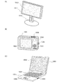
上記実施の形態の各々の図で述べた内容(一部でもよい)を様々な電子機器に適用することができる。具体的には、電子機器の表示部に適用することができる。そのような電子機器として、ビデオカメラ、デジタルカメラなどのカメラ、ゴーグル型ディスプレイ、ナビゲーションシステム、音響再生装置(カーオーディオ、オーディオコンポ等)、コンピュータ、ゲーム機器、携帯情報端末(モバイルコンピュータ、携帯電話、携帯型ゲーム機又は電子書籍等)、記録媒体を備えた画像再生装置(具体的にはDigital Versatile Disc(DVD)等の記録媒体を再生し、その画像を表示しうるディスプレイを備えた装置)などが挙げられる。 The contents (or part of the contents) described in each drawing of the above embodiment can be applied to various electronic devices. Specifically, it can be applied to a display portion of an electronic device. Such electronic devices include cameras such as video cameras and digital cameras, goggle-type displays, navigation systems, sound playback devices (car audio, audio components, etc.), computers, game devices, personal digital assistants (mobile computers, mobile phones, Portable game machines, electronic books, etc.), image playback devices equipped with recording media (specifically, devices equipped with a display capable of playing back recording media such as Digital Versatile Disc (DVD) and displaying the images), etc. Is mentioned.
図10(A)はディスプレイであり、筐体1011、支持台1012、表示部1013を含む。図10(A)に示すディスプレイは、様々な情報(静止画、動画、テキスト画像など)を表示部に表示する機能を有する。なお、図10(A)に示すディスプレイが有する機能はこれに限定されず、様々な機能を有することができる。
FIG. 10A illustrates a display, which includes a
図10(B)はカメラであり、本体1031、表示部1032、受像部1033、操作キー1034、外部接続ポート1035、シャッターボタン1036を含む。図10(B)に示すカメラは、静止画を撮影する機能を有する。動画を撮影する機能を有する。なお、図10(B)に示すカメラが有する機能はこれに限定されず、様々な機能を有することができる。
FIG. 10B illustrates a camera, which includes a
図10(C)はコンピュータであり、本体1051、筐体1052、表示部1053、キーボード1054、外部接続ポート1055、ポインティングデバイス1056を含む。図10(C)に示すコンピュータは、様々な情報(静止画、動画、テキスト画像など)を表示部に表示する機能を有する。なお、図10(C)に示すコンピュータが有する機能はこれに限定されず、様々な機能を有することができる。
FIG. 10C illustrates a computer, which includes a
本実施形態の表示部に上記実施の形態で説明した表示装置を用いる構成とすることで、上述の図10(A)乃至図10(C)の表示部を構成する画素に接続される信号線及び電源線の数を削減することができる。そして信号線に接続された信号線駆動回路において、駆動回路の素子数を削減することができ、低コスト化を図ることができ、表示部での高精細な表示を行うことができる。 By using the display device described in any of the above embodiments for the display portion of this embodiment, a signal line connected to the pixels included in the display portions in FIGS. 10A to 10C described above. In addition, the number of power supply lines can be reduced. In the signal line driver circuit connected to the signal line, the number of elements in the driver circuit can be reduced, the cost can be reduced, and high-definition display on the display portion can be performed.
本実施の形態は、他の実施の形態に記載した構成と適宜組み合わせて実施することが可能である。 This embodiment can be implemented in appropriate combination with the structures described in the other embodiments.
10 パルス出力回路
11 配線
12 配線
13 配線
14 配線
15 配線
16 配線
17 配線
18 配線
21 入力端子
22 入力端子
23 入力端子
24 入力端子
25 入力端子
26 出力端子
27 出力端子
28 入力端子
100 パルス出力回路
101 第1の回路
102 第2の回路
103 第3の回路
105 第1のトランジスタ
104A 第4の回路
104B 第4の回路
106 第2のトランジスタ
107A スイッチ
107B スイッチ
110 配線
111 判定回路
201 定電流源
202 トランジスタ
203 コンパレータ
204 バッファ回路
301 トランジスタ
302 トランジスタ
303 容量素子
304 トランジスタ
305 トランジスタ
306 トランジスタ
307 トランジスタ
308 トランジスタ
309 トランジスタ
401 トランジスタ
402 トランジスタ
501 期間
502 期間
601 ステップ
602 ステップ
603 ステップ
604 ステップ
605 ステップ
606 ステップ
607 ステップ
608 ステップ
609 ステップ
610 ステップ
701 薄膜トランジスタ
702 容量
703 薄膜トランジスタ
704 画素電極層
705 絶縁層
706 基板
707 絶縁層
708 対向電極層
709 着色層
710 対向基板
711 液晶層
712a 偏光板
712b 偏光板
713 端子
714 接続電極
715 端子電極
716 端子
717 端子電極
718 導電層
719b ドレイン電極層
720 導電層
721 ゲート電極層
722 ゲート絶縁層
723 半導体層
724 酸化物絶縁層
1011 筐体
1012 支持台
1013 表示部
101A 第1の回路
101B 第1の回路
1031 本体
1032 表示部
1033 受像部
1034 操作キー
1035 外部接続ポート
1036 シャッターボタン
1051 本体
1052 筐体
1053 表示部
1054 キーボード
1055 外部接続ポート
1056 ポインティングデバイス
108A 第3のトランジスタ
108B 第3のトランジスタ
109A 第4のトランジスタ
109B 第4のトランジスタ
404B 回路
5300 基板
5301 画素部
5302 走査線駆動回路
5303 走査線駆動回路
5304 信号線駆動回路
5305 タイミング制御回路
5306 判定回路
5601 シフトレジスタ
5602 スイッチング回路
5603 薄膜トランジスタ
5604 配線
5605 配線
10 Pulse output circuit 11 Wiring 12 Wiring 13 Wiring 14 Wiring 15 Wiring 16 Wiring 17 Wiring 18 Wiring 21 Input terminal 22 Input terminal 23 Input terminal 24 Input terminal 25 Input terminal 26 Output terminal 27 Output terminal 28 Input terminal 100 Pulse output circuit 101 No. 1 1 circuit 102 2nd circuit 103 3rd circuit 105 1st transistor 104A 4th circuit 104B 4th circuit 106 2nd transistor 107A switch 107B switch 110 wiring 111 judgment circuit 201 constant current source 202 transistor 203 comparator 204 Buffer circuit 301 Transistor 302 Transistor 303 Capacitor 304 Transistor 305 Transistor 306 Transistor 307 Transistor 308 Transistor 309 Transistor 401 Transistor 402 Transistor 501 Period 502 Period 601 Step 602 Step 603 Step 604 Step 605 Step 606 Step 607 Step 608 Step 609 Step 610 Step 701 Thin film transistor 702 Capacitor 703 Thin film transistor 704 Pixel electrode layer 705 Insulating layer 706 Substrate 707 Insulating layer 708 Counter electrode layer 709 Colored layer 710 Counter substrate 711 Liquid crystal layer 712a Polarizing plate 712b Polarizing plate 713 Terminal 714 Connection electrode 715 Terminal electrode 716 Terminal 717 Terminal electrode 718 Conductive layer 719b Drain electrode layer 720 Conductive layer 721 Gate electrode layer 722 Gate insulating layer 723 Semiconductor layer 724 Oxide insulating Layer 1011 Housing 1012 Support base 1013 Display unit 101A First circuit 101B First circuit 1031 Main body 1032 Display unit 1 33 Image receiver 1034 Operation key 1035 External connection port 1036 Shutter button 1051 Main body 1052 Case 1053 Display unit 1054 Keyboard 1055 External connection port 1056 Pointing device 108A Third transistor 108B Third transistor 109A Fourth transistor 109B Fourth transistor 404B circuit 5300 substrate 5301 pixel portion 5302 scanning line driving circuit 5303 scanning line driving circuit 5304 signal line driving circuit 5305 timing control circuit 5306 determination circuit 5601 shift register 5602 switching circuit 5603 thin film transistor 5604 wiring 5605 wiring
Claims (9)
前記パルス出力回路は、
第1のノード及び第2のノードの電位に応じて出力信号を出力することができる機能を有する第1の回路と、
前記第1のノードに、前段のパルス出力回路の出力信号に応じた信号を供給することができる機能を有する第2の回路と、
前記第2のノードに間欠的に高電源電位の信号を供給することができる機能を有する第3の回路と、
前記第2のノードがゲートに電気的に接続され、前記第2のノードの電位に応じて、前記第1のノードの電位を制御することができる機能を有する第1のトランジスタと、
前記前段のパルス出力回路の出力信号に応じた信号がゲートに供給され、前記第2のノードの電位を制御することができる機能を有する第2のトランジスタと、
前記第1のトランジスタのソース端子と、低電源電位を供給することができる機能を有する配線との間に、前記第1のトランジスタのソース端子の電位を低電源電位より昇圧することができる機能を有する第4の回路と、
前記第2のトランジスタのソース端子と、低電源電位を供給することができる機能を有する前記配線との間に、前記第2のトランジスタのソース端子の電位を低電源電位より昇圧することができる機能を有する第5の回路と、
前記第1のトランジスタのソース端子の電位を低電源電位にすることができる機能を有する第1のスイッチと、
前記第2のトランジスタのソース端子の電位を低電源電位にすることができる機能を有する第2のスイッチと、を有し、
前記第1のトランジスタ及び前記第2のトランジスタは、チャネル領域に酸化物半導体を有し、
前記第1のスイッチ及び前記第2のスイッチは、前記第1のトランジスタ及び前記第2のトランジスタがエンハンスメント型、またはディプレッション型であるかを判定することができる機能を有する判定回路によって制御されることを特徴とする駆動回路。 Have a pulse output circuit of the plurality of stages,
The pulse output circuit includes:
A first circuit having a function of outputting an output signal in accordance with the potentials of the first node and the second node;
A second circuit having a function capable of supplying a signal corresponding to an output signal of a preceding pulse output circuit to the first node;
A third circuit having a function capable of intermittently supplying a signal of a high power supply potential to the second node;
A first transistor having a function of controlling the potential of the first node according to the potential of the second node, wherein the second node is electrically connected to a gate;
A second transistor having a function of controlling a potential of the second node by supplying a signal corresponding to an output signal of the pulse output circuit in the previous stage to the gate ;
And the source terminal of the pre-Symbol first transistors comprising, between the wiring having a function capable to supply a low power supply potential, the potential of the source terminal of the first transistor can be boosted from the low power supply potential A fourth circuit having a function ;
A function capable of boosting the potential of the source terminal of the second transistor from the low power supply potential between the source terminal of the second transistor and the wiring having a function of supplying a low power supply potential. A fifth circuit having:
A first switch having a function capable of setting a potential of a source terminal of the first transistor to a low power supply potential ;
A second switch having a function of allowing the potential of the source terminal of the second transistor to be a low power supply potential ;
The first transistor and the second transistor each include an oxide semiconductor in a channel region;
Said first switch and said second switch, Gosei the first transistor and the second transistor by the decision circuit having a function capable determines whether the enhancement or depletion type, A driving circuit.
前記パルス出力回路は、The pulse output circuit includes:
第1のノード及び第2のノードの電位に応じて出力信号を出力することができる機能を有する第1の回路と、A first circuit having a function of outputting an output signal in accordance with the potentials of the first node and the second node;
前記第1のノードに、前段のパルス出力回路の出力信号に応じた信号を供給することができる機能を有する第2の回路と、A second circuit having a function capable of supplying a signal corresponding to an output signal of a preceding pulse output circuit to the first node;
前記第2のノードに間欠的に高電源電位の信号を供給することができる機能を有する第3の回路と、A third circuit having a function capable of intermittently supplying a signal of a high power supply potential to the second node;
前記第2のノードがゲートに電気的に接続され、前記第2のノードの電位に応じて、前記第1のノードの電位を制御することができる機能を有する第1のトランジスタと、A first transistor having a function of controlling the potential of the first node according to the potential of the second node, wherein the second node is electrically connected to a gate;
前記前段のパルス出力回路の出力信号に応じた信号がゲートに供給され、前記第2のノードの電位を制御することができる機能を有する第2のトランジスタと、A second transistor having a function of controlling a potential of the second node by supplying a signal corresponding to an output signal of the pulse output circuit in the previous stage to the gate;
前記第1のトランジスタのソース端子と、低電源電位を供給することができる機能を有する配線との間に、前記第1のトランジスタのソース端子の電位を低電源電位より昇圧することができる機能を有する第4の回路と、A function capable of boosting the potential of the source terminal of the first transistor from the low power supply potential between the source terminal of the first transistor and a wiring having a function of supplying a low power supply potential. A fourth circuit comprising:
前記第2のトランジスタのソース端子と、低電源電位を供給することができる機能を有する前記配線との間に、前記第2のトランジスタのソース端子の電位を低電源電位より昇圧することができる機能を有する第5の回路と、A function capable of boosting the potential of the source terminal of the second transistor from the low power supply potential between the source terminal of the second transistor and the wiring having a function of supplying a low power supply potential. A fifth circuit having:
前記第1のトランジスタのソース端子の電位を低電源電位にすることができる機能を有する第1のスイッチと、A first switch having a function capable of setting a potential of a source terminal of the first transistor to a low power supply potential;
前記第2のトランジスタのソース端子の電位を低電源電位にすることができる機能を有する第2のスイッチと、を有し、A second switch having a function of allowing the potential of the source terminal of the second transistor to be a low power supply potential;
前記第1のスイッチ及び前記第2のスイッチは、前記第1のトランジスタ及び前記第2のトランジスタがエンハンスメント型、またはディプレッション型であるかを判定することができる機能を有する判定回路によって制御されることを特徴とする駆動回路。The first switch and the second switch are controlled by a determination circuit having a function of determining whether the first transistor and the second transistor are an enhancement type or a depletion type. A drive circuit characterized by the above.
前記第4の回路は、ゲートとドレイン端子が電気的に接続され、ソース端子が前記配線に電気的に接続された第3のトランジスタを有し、
前記第5の回路は、ゲートとドレイン端子が電気的に接続され、ソース端子が前記配線に電気的に接続された第4のトランジスタを有することを特徴とする駆動回路。 In claim 1 or claim 2 ,
Said fourth circuit, the gate and drain terminals are electrically connected, have a third transistor having a source terminal electrically connected to the wiring,
The fifth circuit has a gate and a drain terminal electrically connected to a driving circuit, wherein the benzalkonium to have a fourth transistor having a source terminal electrically connected to the wiring.
前記第3のトランジスタのL/Wは、前記第1のトランジスタのL/Wより大きく、かつ前記第2のトランジスタのL/Wより大きく、
前記第4のトランジスタのL/Wは、前記第1のトランジスタのL/Wより大きく、かつ前記第2のトランジスタのL/Wより大きいことを特徴とする駆動回路。 In claim 3 ,
L / W of the third transistor is greater than L / W of the first transistor, and rather greater than L / W of the second transistor,
The L / W of the fourth transistor, wherein greater than L / W of the first transistor, and a driving circuit, wherein the magnitude Ikoto than L / W of the second transistor.
前記第3のトランジスタ及び前記第4のトランジスタは、チャネル領域に酸化物半導体を有することを特徴とする駆動回路。The third transistor and the fourth transistor each include an oxide semiconductor in a channel region.
前記判定回路は、定電流源、トランジスタ、コンパレータ、及びバッファ回路を有することを特徴とする駆動回路。 In any one of claims 1 to 5,
The determination circuit includes a constant current source, a transistor, a comparator, and a buffer circuit.
前記第1のスイッチ及び前記第2のスイッチはそれぞれトランジスタで構成され、該トランジスタのチャネル領域は酸化物半導体を有することを特徴とする駆動回路。 In any one of Claims 1 thru | or 6 ,
Each of the first switch and the second switch includes a transistor, and a channel region of the transistor includes an oxide semiconductor .
An electronic apparatus comprising the display device according to claim 8 .
Priority Applications (1)
| Application Number | Priority Date | Filing Date | Title |
|---|---|---|---|
| JP2010202554A JP5084887B2 (en) | 2009-09-16 | 2010-09-10 | Drive circuit, display device including the drive circuit, and electronic device including the display device |
Applications Claiming Priority (3)
| Application Number | Priority Date | Filing Date | Title |
|---|---|---|---|
| JP2009214297 | 2009-09-16 | ||
| JP2009214297 | 2009-09-16 | ||
| JP2010202554A JP5084887B2 (en) | 2009-09-16 | 2010-09-10 | Drive circuit, display device including the drive circuit, and electronic device including the display device |
Related Child Applications (1)
| Application Number | Title | Priority Date | Filing Date |
|---|---|---|---|
| JP2012193861A Division JP5380595B2 (en) | 2009-09-16 | 2012-09-04 | Driving circuit |
Publications (3)
| Publication Number | Publication Date |
|---|---|
| JP2011086363A JP2011086363A (en) | 2011-04-28 |
| JP2011086363A5 JP2011086363A5 (en) | 2012-09-13 |
| JP5084887B2 true JP5084887B2 (en) | 2012-11-28 |
Family
ID=43730543
Family Applications (4)
| Application Number | Title | Priority Date | Filing Date |
|---|---|---|---|
| JP2010202554A Active JP5084887B2 (en) | 2009-09-16 | 2010-09-10 | Drive circuit, display device including the drive circuit, and electronic device including the display device |
| JP2012193861A Expired - Fee Related JP5380595B2 (en) | 2009-09-16 | 2012-09-04 | Driving circuit |
| JP2013199665A Active JP5600792B2 (en) | 2009-09-16 | 2013-09-26 | Driving circuit |
| JP2014161149A Expired - Fee Related JP5809336B2 (en) | 2009-09-16 | 2014-08-07 | Driving circuit |
Family Applications After (3)
| Application Number | Title | Priority Date | Filing Date |
|---|---|---|---|
| JP2012193861A Expired - Fee Related JP5380595B2 (en) | 2009-09-16 | 2012-09-04 | Driving circuit |
| JP2013199665A Active JP5600792B2 (en) | 2009-09-16 | 2013-09-26 | Driving circuit |
| JP2014161149A Expired - Fee Related JP5809336B2 (en) | 2009-09-16 | 2014-08-07 | Driving circuit |
Country Status (5)
| Country | Link |
|---|---|
| US (1) | US8427417B2 (en) |
| JP (4) | JP5084887B2 (en) |
| KR (1) | KR101700470B1 (en) |
| TW (1) | TWI492208B (en) |
| WO (1) | WO2011033909A1 (en) |
Families Citing this family (19)
| Publication number | Priority date | Publication date | Assignee | Title |
|---|---|---|---|---|
| WO2012153697A1 (en) | 2011-05-06 | 2012-11-15 | Semiconductor Energy Laboratory Co., Ltd. | Semiconductor memory device |
| US9466618B2 (en) | 2011-05-13 | 2016-10-11 | Semiconductor Energy Laboratory Co., Ltd. | Semiconductor device including two thin film transistors and method of manufacturing the same |
| TWI501226B (en) * | 2011-05-20 | 2015-09-21 | Semiconductor Energy Lab | Memory device and method for driving memory device |
| JP6116149B2 (en) | 2011-08-24 | 2017-04-19 | 株式会社半導体エネルギー研究所 | Semiconductor device |
| TWI668839B (en) * | 2011-08-29 | 2019-08-11 | 日商半導體能源研究所股份有限公司 | Semiconductor device |
| TWI462075B (en) | 2012-01-20 | 2014-11-21 | Hung Ta Liu | A driving method and a display structure using the driving method |
| JPWO2013160941A1 (en) * | 2012-04-25 | 2015-12-21 | 株式会社Joled | Shift register and display device |
| US9742378B2 (en) | 2012-06-29 | 2017-08-22 | Semiconductor Energy Laboratory Co., Ltd. | Pulse output circuit and semiconductor device |
| TWI635501B (en) | 2012-07-20 | 2018-09-11 | 半導體能源研究所股份有限公司 | Pulse output circuit, display device, and electronic device |
| JP6475424B2 (en) | 2013-06-05 | 2019-02-27 | 株式会社半導体エネルギー研究所 | Semiconductor device |
| US9583063B2 (en) | 2013-09-12 | 2017-02-28 | Semiconductor Energy Laboratory Co., Ltd. | Display device |
| US11266981B2 (en) * | 2013-12-02 | 2022-03-08 | Johnson Matthey Public Limited Company | Mixed template synthesis of low silica CHA zeolite |
| BR112016012390B1 (en) * | 2013-12-02 | 2021-05-04 | Johnson Matthey Public Limited Company | catalyst composition, methods for synthesizing a catalyst composition and for treating an exhaust gas, and catalyst article |
| JP6416650B2 (en) * | 2015-02-06 | 2018-10-31 | エイブリック株式会社 | Constant voltage circuit and oscillation device |
| WO2018003931A1 (en) * | 2016-07-01 | 2018-01-04 | シャープ株式会社 | Tft circuit and shift register circuit |
| CN107993603B (en) * | 2016-10-27 | 2023-08-18 | 合肥鑫晟光电科技有限公司 | Shift register unit, shift register, gate driving circuit and display device |
| TWI615824B (en) * | 2017-02-20 | 2018-02-21 | 友達光電股份有限公司 | Display panel and driving circuit thereof |
| TWI686786B (en) * | 2017-04-17 | 2020-03-01 | 世界先進積體電路股份有限公司 | display system |
| US20190019472A1 (en) | 2017-07-13 | 2019-01-17 | Vanguard International Semiconductor Corporation | Display system and method for forming an output buffer of a source driver |
Family Cites Families (117)
| Publication number | Priority date | Publication date | Assignee | Title |
|---|---|---|---|---|
| JPH01233914A (en) * | 1988-03-15 | 1989-09-19 | Fujitsu Ltd | Integrated circuit comprising dcfl basic logic element |
| JPH086653A (en) * | 1994-06-16 | 1996-01-12 | Sony Corp | Reference voltage generating circuit |
| EP0820644B1 (en) * | 1995-08-03 | 2005-08-24 | Koninklijke Philips Electronics N.V. | Semiconductor device provided with transparent switching element |
| JPH09116408A (en) * | 1995-10-19 | 1997-05-02 | Hitachi Ltd | Semiconductor integrated circuit |
| JP3625598B2 (en) * | 1995-12-30 | 2005-03-02 | 三星電子株式会社 | Manufacturing method of liquid crystal display device |
| JP4170454B2 (en) | 1998-07-24 | 2008-10-22 | Hoya株式会社 | Article having transparent conductive oxide thin film and method for producing the same |
| JP2000150861A (en) * | 1998-11-16 | 2000-05-30 | Tdk Corp | Oxide thin film |
| JP3276930B2 (en) * | 1998-11-17 | 2002-04-22 | 科学技術振興事業団 | Transistor and semiconductor device |
| TW460731B (en) * | 1999-09-03 | 2001-10-21 | Ind Tech Res Inst | Electrode structure and production method of wide viewing angle LCD |
| US7633471B2 (en) * | 2000-05-12 | 2009-12-15 | Semiconductor Energy Laboratory Co., Ltd. | Light-emitting device and electric appliance |
| JP4089858B2 (en) | 2000-09-01 | 2008-05-28 | 国立大学法人東北大学 | Semiconductor device |
| JP2002133890A (en) * | 2000-10-24 | 2002-05-10 | Alps Electric Co Ltd | Shift register |
| KR20020038482A (en) * | 2000-11-15 | 2002-05-23 | 모리시타 요이찌 | Thin film transistor array, method for producing the same, and display panel using the same |
| KR100788391B1 (en) * | 2001-02-27 | 2007-12-31 | 엘지.필립스 엘시디 주식회사 | Circuit for bi-directional driving liquid crystal display panel |
| JP3997731B2 (en) * | 2001-03-19 | 2007-10-24 | 富士ゼロックス株式会社 | Method for forming a crystalline semiconductor thin film on a substrate |
| JP2002289859A (en) | 2001-03-23 | 2002-10-04 | Minolta Co Ltd | Thin-film transistor |
| US7218349B2 (en) | 2001-08-09 | 2007-05-15 | Semiconductor Energy Laboratory Co., Ltd. | Semiconductor device |
| JP3925839B2 (en) | 2001-09-10 | 2007-06-06 | シャープ株式会社 | Semiconductor memory device and test method thereof |
| JP4090716B2 (en) | 2001-09-10 | 2008-05-28 | 雅司 川崎 | Thin film transistor and matrix display device |
| JP4164562B2 (en) | 2002-09-11 | 2008-10-15 | 独立行政法人科学技術振興機構 | Transparent thin film field effect transistor using homologous thin film as active layer |
| WO2003040441A1 (en) * | 2001-11-05 | 2003-05-15 | Japan Science And Technology Agency | Natural superlattice homologous single crystal thin film, method for preparation thereof, and device using said single crystal thin film |
| JP4083486B2 (en) * | 2002-02-21 | 2008-04-30 | 独立行政法人科学技術振興機構 | Method for producing LnCuO (S, Se, Te) single crystal thin film |
| CN1445821A (en) * | 2002-03-15 | 2003-10-01 | 三洋电机株式会社 | Forming method of ZnO film and ZnO semiconductor layer, semiconductor element and manufacturing method thereof |
| JP3933591B2 (en) * | 2002-03-26 | 2007-06-20 | 淳二 城戸 | Organic electroluminescent device |
| US7339187B2 (en) * | 2002-05-21 | 2008-03-04 | State Of Oregon Acting By And Through The Oregon State Board Of Higher Education On Behalf Of Oregon State University | Transistor structures |
| JP2004022625A (en) * | 2002-06-13 | 2004-01-22 | Murata Mfg Co Ltd | Manufacturing method of semiconductor device and its manufacturing method |
| US7105868B2 (en) | 2002-06-24 | 2006-09-12 | Cermet, Inc. | High-electron mobility transistor with zinc oxide |
| US7067843B2 (en) * | 2002-10-11 | 2006-06-27 | E. I. Du Pont De Nemours And Company | Transparent oxide semiconductor thin film transistors |
| JP4339103B2 (en) * | 2002-12-25 | 2009-10-07 | 株式会社半導体エネルギー研究所 | Semiconductor device and display device |
| JP4166105B2 (en) | 2003-03-06 | 2008-10-15 | シャープ株式会社 | Semiconductor device and manufacturing method thereof |
| JP2004273732A (en) | 2003-03-07 | 2004-09-30 | Sharp Corp | Active matrix substrate and its producing process |
| JP4531343B2 (en) | 2003-03-26 | 2010-08-25 | 株式会社半導体エネルギー研究所 | Driving circuit |
| JP4108633B2 (en) | 2003-06-20 | 2008-06-25 | シャープ株式会社 | THIN FILM TRANSISTOR, MANUFACTURING METHOD THEREOF, AND ELECTRONIC DEVICE |
| US7486269B2 (en) * | 2003-07-09 | 2009-02-03 | Samsung Electronics Co., Ltd. | Shift register, scan driving circuit and display apparatus having the same |
| US7262463B2 (en) * | 2003-07-25 | 2007-08-28 | Hewlett-Packard Development Company, L.P. | Transistor including a deposited channel region having a doped portion |
| DE102004038800A1 (en) * | 2003-08-13 | 2005-03-31 | Dsm Ip Assets B.V. | Production of tocol, tocol derivatives and tocopherols |
| JP2005251348A (en) | 2004-03-08 | 2005-09-15 | Casio Comput Co Ltd | Shift register circuit and its driving control method |
| CN1998087B (en) | 2004-03-12 | 2014-12-31 | 独立行政法人科学技术振兴机构 | Amorphous oxide and thin film transistor |
| US7145174B2 (en) * | 2004-03-12 | 2006-12-05 | Hewlett-Packard Development Company, Lp. | Semiconductor device |
| US7297977B2 (en) * | 2004-03-12 | 2007-11-20 | Hewlett-Packard Development Company, L.P. | Semiconductor device |
| US7282782B2 (en) * | 2004-03-12 | 2007-10-16 | Hewlett-Packard Development Company, L.P. | Combined binary oxide semiconductor device |
| US7211825B2 (en) * | 2004-06-14 | 2007-05-01 | Yi-Chi Shih | Indium oxide-based thin film transistors and circuits |
| JP2006100760A (en) * | 2004-09-02 | 2006-04-13 | Casio Comput Co Ltd | Thin-film transistor and its manufacturing method |
| US7285501B2 (en) * | 2004-09-17 | 2007-10-23 | Hewlett-Packard Development Company, L.P. | Method of forming a solution processed device |
| US7298084B2 (en) * | 2004-11-02 | 2007-11-20 | 3M Innovative Properties Company | Methods and displays utilizing integrated zinc oxide row and column drivers in conjunction with organic light emitting diodes |
| US7453065B2 (en) * | 2004-11-10 | 2008-11-18 | Canon Kabushiki Kaisha | Sensor and image pickup device |
| US7829444B2 (en) * | 2004-11-10 | 2010-11-09 | Canon Kabushiki Kaisha | Field effect transistor manufacturing method |
| RU2399989C2 (en) * | 2004-11-10 | 2010-09-20 | Кэнон Кабусики Кайся | Amorphous oxide and field-effect transistor using said oxide |
| WO2006051994A2 (en) * | 2004-11-10 | 2006-05-18 | Canon Kabushiki Kaisha | Light-emitting device |
| US7791072B2 (en) * | 2004-11-10 | 2010-09-07 | Canon Kabushiki Kaisha | Display |
| US7863611B2 (en) * | 2004-11-10 | 2011-01-04 | Canon Kabushiki Kaisha | Integrated circuits utilizing amorphous oxides |
| US7868326B2 (en) * | 2004-11-10 | 2011-01-11 | Canon Kabushiki Kaisha | Field effect transistor |
| US7579224B2 (en) * | 2005-01-21 | 2009-08-25 | Semiconductor Energy Laboratory Co., Ltd. | Method for manufacturing a thin film semiconductor device |
| TWI412138B (en) * | 2005-01-28 | 2013-10-11 | Semiconductor Energy Lab | Semiconductor device, electronic device, and method of manufacturing semiconductor device |
| TWI569441B (en) * | 2005-01-28 | 2017-02-01 | 半導體能源研究所股份有限公司 | Semiconductor device, electronic device, and method of manufacturing semiconductor device |
| US7858451B2 (en) * | 2005-02-03 | 2010-12-28 | Semiconductor Energy Laboratory Co., Ltd. | Electronic device, semiconductor device and manufacturing method thereof |
| US7948171B2 (en) * | 2005-02-18 | 2011-05-24 | Semiconductor Energy Laboratory Co., Ltd. | Light emitting device |
| US20060197092A1 (en) * | 2005-03-03 | 2006-09-07 | Randy Hoffman | System and method for forming conductive material on a substrate |
| US8681077B2 (en) * | 2005-03-18 | 2014-03-25 | Semiconductor Energy Laboratory Co., Ltd. | Semiconductor device, and display device, driving method and electronic apparatus thereof |
| WO2006105077A2 (en) * | 2005-03-28 | 2006-10-05 | Massachusetts Institute Of Technology | Low voltage thin film transistor with high-k dielectric material |
| JP4993544B2 (en) * | 2005-03-30 | 2012-08-08 | 三菱電機株式会社 | Shift register circuit |
| US7645478B2 (en) * | 2005-03-31 | 2010-01-12 | 3M Innovative Properties Company | Methods of making displays |
| US8300031B2 (en) * | 2005-04-20 | 2012-10-30 | Semiconductor Energy Laboratory Co., Ltd. | Semiconductor device comprising transistor having gate and drain connected through a current-voltage conversion element |
| JP2006344849A (en) * | 2005-06-10 | 2006-12-21 | Casio Comput Co Ltd | Thin film transistor |
| US7691666B2 (en) * | 2005-06-16 | 2010-04-06 | Eastman Kodak Company | Methods of making thin film transistors comprising zinc-oxide-based semiconductor materials and transistors made thereby |
| US7402506B2 (en) * | 2005-06-16 | 2008-07-22 | Eastman Kodak Company | Methods of making thin film transistors comprising zinc-oxide-based semiconductor materials and transistors made thereby |
| US7507618B2 (en) * | 2005-06-27 | 2009-03-24 | 3M Innovative Properties Company | Method for making electronic devices using metal oxide nanoparticles |
| JP2007018299A (en) * | 2005-07-08 | 2007-01-25 | Mitsubishi Electric Corp | Voltage generation circuit and display device |
| KR100711890B1 (en) * | 2005-07-28 | 2007-04-25 | 삼성에스디아이 주식회사 | Organic Light Emitting Display and Fabrication Method for the same |
| JP2007059128A (en) * | 2005-08-23 | 2007-03-08 | Canon Inc | Organic electroluminescent display device and manufacturing method thereof |
| JP4280736B2 (en) * | 2005-09-06 | 2009-06-17 | キヤノン株式会社 | Semiconductor element |
| JP4850457B2 (en) * | 2005-09-06 | 2012-01-11 | キヤノン株式会社 | Thin film transistor and thin film diode |
| JP2007073705A (en) * | 2005-09-06 | 2007-03-22 | Canon Inc | Oxide-semiconductor channel film transistor and its method of manufacturing same |
| JP5116225B2 (en) * | 2005-09-06 | 2013-01-09 | キヤノン株式会社 | Manufacturing method of oxide semiconductor device |
| EP1995787A3 (en) * | 2005-09-29 | 2012-01-18 | Semiconductor Energy Laboratory Co, Ltd. | Semiconductor device having oxide semiconductor layer and manufacturing method therof |
| US7310402B2 (en) * | 2005-10-18 | 2007-12-18 | Au Optronics Corporation | Gate line drivers for active matrix displays |
| US9153341B2 (en) | 2005-10-18 | 2015-10-06 | Semiconductor Energy Laboratory Co., Ltd. | Shift register, semiconductor device, display device, and electronic device |
| JP5037808B2 (en) * | 2005-10-20 | 2012-10-03 | キヤノン株式会社 | Field effect transistor using amorphous oxide, and display device using the transistor |
| CN101577282A (en) * | 2005-11-15 | 2009-11-11 | 株式会社半导体能源研究所 | Semiconductor device and method of manufacturing the same |
| TWI292281B (en) * | 2005-12-29 | 2008-01-01 | Ind Tech Res Inst | Pixel structure of active organic light emitting diode and method of fabricating the same |
| JP2007207411A (en) * | 2006-01-05 | 2007-08-16 | Mitsubishi Electric Corp | Shift register circuit and image display device provided with the same |
| US7867636B2 (en) * | 2006-01-11 | 2011-01-11 | Murata Manufacturing Co., Ltd. | Transparent conductive film and method for manufacturing the same |
| JP4977478B2 (en) * | 2006-01-21 | 2012-07-18 | 三星電子株式会社 | ZnO film and method of manufacturing TFT using the same |
| US7576394B2 (en) * | 2006-02-02 | 2009-08-18 | Kochi Industrial Promotion Center | Thin film transistor including low resistance conductive thin films and manufacturing method thereof |
| US7977169B2 (en) * | 2006-02-15 | 2011-07-12 | Kochi Industrial Promotion Center | Semiconductor device including active layer made of zinc oxide with controlled orientations and manufacturing method thereof |
| KR20070101595A (en) * | 2006-04-11 | 2007-10-17 | 삼성전자주식회사 | Zno thin film transistor |
| US20070252928A1 (en) * | 2006-04-28 | 2007-11-01 | Toppan Printing Co., Ltd. | Structure, transmission type liquid crystal display, reflection type display and manufacturing method thereof |
| JP5028033B2 (en) * | 2006-06-13 | 2012-09-19 | キヤノン株式会社 | Oxide semiconductor film dry etching method |
| JP4609797B2 (en) * | 2006-08-09 | 2011-01-12 | Nec液晶テクノロジー株式会社 | Thin film device and manufacturing method thereof |
| JP4999400B2 (en) * | 2006-08-09 | 2012-08-15 | キヤノン株式会社 | Oxide semiconductor film dry etching method |
| JP4332545B2 (en) * | 2006-09-15 | 2009-09-16 | キヤノン株式会社 | Field effect transistor and manufacturing method thereof |
| JP4274219B2 (en) * | 2006-09-27 | 2009-06-03 | セイコーエプソン株式会社 | Electronic devices, organic electroluminescence devices, organic thin film semiconductor devices |
| JP5164357B2 (en) * | 2006-09-27 | 2013-03-21 | キヤノン株式会社 | Semiconductor device and manufacturing method of semiconductor device |
| JP4932415B2 (en) * | 2006-09-29 | 2012-05-16 | 株式会社半導体エネルギー研究所 | Semiconductor device |
| TWI651701B (en) | 2006-09-29 | 2019-02-21 | 日商半導體能源研究所股份有限公司 | Display device and electronic device |
| JP5116277B2 (en) * | 2006-09-29 | 2013-01-09 | 株式会社半導体エネルギー研究所 | Semiconductor device, display device, liquid crystal display device, display module, and electronic apparatus |
| US7622371B2 (en) * | 2006-10-10 | 2009-11-24 | Hewlett-Packard Development Company, L.P. | Fused nanocrystal thin film semiconductor and method |
| US7772021B2 (en) * | 2006-11-29 | 2010-08-10 | Samsung Electronics Co., Ltd. | Flat panel displays comprising a thin-film transistor having a semiconductive oxide in its channel and methods of fabricating the same for use in flat panel displays |
| JP2008140684A (en) * | 2006-12-04 | 2008-06-19 | Toppan Printing Co Ltd | Color el display, and its manufacturing method |
| TWI383348B (en) * | 2006-12-05 | 2013-01-21 | Chunghwa Picture Tubes Ltd | Shift register, driving circuit, and display device thereof |
| TWI346320B (en) * | 2006-12-26 | 2011-08-01 | Au Optronics Corp | Gate driving circuit and driving method thereof |
| KR101303578B1 (en) * | 2007-01-05 | 2013-09-09 | 삼성전자주식회사 | Etching method of thin film |
| US8207063B2 (en) * | 2007-01-26 | 2012-06-26 | Eastman Kodak Company | Process for atomic layer deposition |
| KR100851215B1 (en) * | 2007-03-14 | 2008-08-07 | 삼성에스디아이 주식회사 | Thin film transistor and organic light-emitting dislplay device having the thin film transistor |
| TWI453711B (en) * | 2007-03-21 | 2014-09-21 | Semiconductor Energy Lab | Display device |
| US7795613B2 (en) * | 2007-04-17 | 2010-09-14 | Toppan Printing Co., Ltd. | Structure with transistor |
| KR101325053B1 (en) * | 2007-04-18 | 2013-11-05 | 삼성디스플레이 주식회사 | Thin film transistor substrate and manufacturing method thereof |
| KR20080094300A (en) * | 2007-04-19 | 2008-10-23 | 삼성전자주식회사 | Thin film transistor and method of manufacturing the same and flat panel display comprising the same |
| KR101334181B1 (en) * | 2007-04-20 | 2013-11-28 | 삼성전자주식회사 | Thin Film Transistor having selectively crystallized channel layer and method of manufacturing the same |
| KR101345376B1 (en) * | 2007-05-29 | 2013-12-24 | 삼성전자주식회사 | Fabrication method of ZnO family Thin film transistor |
| JP5245292B2 (en) * | 2007-05-30 | 2013-07-24 | カシオ計算機株式会社 | Shift register circuit and display device |
| JP4715833B2 (en) * | 2007-11-07 | 2011-07-06 | ソニー株式会社 | Display device, display device driving method, and electronic apparatus |
| US8202365B2 (en) * | 2007-12-17 | 2012-06-19 | Fujifilm Corporation | Process for producing oriented inorganic crystalline film, and semiconductor device using the oriented inorganic crystalline film |
| US8314765B2 (en) | 2008-06-17 | 2012-11-20 | Semiconductor Energy Laboratory Co., Ltd. | Driver circuit, display device, and electronic device |
| KR101959185B1 (en) | 2008-11-28 | 2019-03-15 | 가부시키가이샤 한도오따이 에네루기 켄큐쇼 | Semiconductor device, display device and electronic device including the same |
| WO2011071573A2 (en) * | 2009-09-02 | 2011-06-16 | Arizona Board Of Regents, For And On Behalf Of Arizona State University | Amplifiers with depletion and enhancement mode thin film transistors and related methods |
| WO2011052368A1 (en) | 2009-10-30 | 2011-05-05 | Semiconductor Energy Laboratory Co., Ltd. | Driver circuit, display device including the driver circuit, and electronic device including the display device |
-
2010
- 2010-08-18 WO PCT/JP2010/064320 patent/WO2011033909A1/en active Application Filing
- 2010-08-18 KR KR1020127005944A patent/KR101700470B1/en active IP Right Grant
- 2010-09-07 TW TW099130197A patent/TWI492208B/en not_active IP Right Cessation
- 2010-09-08 US US12/877,705 patent/US8427417B2/en not_active Expired - Fee Related
- 2010-09-10 JP JP2010202554A patent/JP5084887B2/en active Active
-
2012
- 2012-09-04 JP JP2012193861A patent/JP5380595B2/en not_active Expired - Fee Related
-
2013
- 2013-09-26 JP JP2013199665A patent/JP5600792B2/en active Active
-
2014
- 2014-08-07 JP JP2014161149A patent/JP5809336B2/en not_active Expired - Fee Related
Also Published As
| Publication number | Publication date |
|---|---|
| JP5600792B2 (en) | 2014-10-01 |
| JP5809336B2 (en) | 2015-11-10 |
| JP2014060726A (en) | 2014-04-03 |
| KR20120083309A (en) | 2012-07-25 |
| TW201133459A (en) | 2011-10-01 |
| US20110064186A1 (en) | 2011-03-17 |
| WO2011033909A1 (en) | 2011-03-24 |
| TWI492208B (en) | 2015-07-11 |
| JP5380595B2 (en) | 2014-01-08 |
| KR101700470B1 (en) | 2017-01-26 |
| US8427417B2 (en) | 2013-04-23 |
| JP2013030263A (en) | 2013-02-07 |
| JP2015027089A (en) | 2015-02-05 |
| JP2011086363A (en) | 2011-04-28 |
Similar Documents
| Publication | Publication Date | Title |
|---|---|---|
| JP5084887B2 (en) | Drive circuit, display device including the drive circuit, and electronic device including the display device | |
| KR101712340B1 (en) | Driver circuit, display device including the driver circuit, and electronic device including the display device | |
| JP5372268B2 (en) | Scanning signal line driving circuit, display device including the same, and scanning signal line driving method | |
| US20150029082A1 (en) | Gate drive circuit and display apparatus having the same | |
| JP6074077B2 (en) | Semiconductor device | |
| TWI529682B (en) | A scanning signal line driving circuit, a display device including the same, and a driving method of a scanning signal line | |
| WO2019184323A1 (en) | Shift register unit, gate driving circuit, display device, and driving method | |
| JP2019191396A (en) | Display device | |
| JP2014191836A (en) | Shift register circuit and image display device | |
| US20230343285A1 (en) | Shift Register Unit and Driving Method Thereof, Gate Driving Circuit, and Display Panel |
Legal Events
| Date | Code | Title | Description |
|---|---|---|---|
| A521 | Request for written amendment filed |
Free format text: JAPANESE INTERMEDIATE CODE: A523 Effective date: 20120727 |
|
| A621 | Written request for application examination |
Free format text: JAPANESE INTERMEDIATE CODE: A621 Effective date: 20120727 |
|
| A871 | Explanation of circumstances concerning accelerated examination |
Free format text: JAPANESE INTERMEDIATE CODE: A871 Effective date: 20120727 |
|
| A975 | Report on accelerated examination |
Free format text: JAPANESE INTERMEDIATE CODE: A971005 Effective date: 20120821 |
|
| TRDD | Decision of grant or rejection written | ||
| A01 | Written decision to grant a patent or to grant a registration (utility model) |
Free format text: JAPANESE INTERMEDIATE CODE: A01 Effective date: 20120828 |
|
| A01 | Written decision to grant a patent or to grant a registration (utility model) |
Free format text: JAPANESE INTERMEDIATE CODE: A01 |
|
| A61 | First payment of annual fees (during grant procedure) |
Free format text: JAPANESE INTERMEDIATE CODE: A61 Effective date: 20120904 |
|
| R150 | Certificate of patent or registration of utility model |
Ref document number: 5084887 Country of ref document: JP Free format text: JAPANESE INTERMEDIATE CODE: R150 Free format text: JAPANESE INTERMEDIATE CODE: R150 |
|
| FPAY | Renewal fee payment (event date is renewal date of database) |
Free format text: PAYMENT UNTIL: 20150914 Year of fee payment: 3 |
|
| FPAY | Renewal fee payment (event date is renewal date of database) |
Free format text: PAYMENT UNTIL: 20150914 Year of fee payment: 3 |
|
| R250 | Receipt of annual fees |
Free format text: JAPANESE INTERMEDIATE CODE: R250 |
|
| R250 | Receipt of annual fees |
Free format text: JAPANESE INTERMEDIATE CODE: R250 |
|
| R250 | Receipt of annual fees |
Free format text: JAPANESE INTERMEDIATE CODE: R250 |
|
| R250 | Receipt of annual fees |
Free format text: JAPANESE INTERMEDIATE CODE: R250 |
|
| R250 | Receipt of annual fees |
Free format text: JAPANESE INTERMEDIATE CODE: R250 |
|
| R250 | Receipt of annual fees |
Free format text: JAPANESE INTERMEDIATE CODE: R250 |
|
| R250 | Receipt of annual fees |
Free format text: JAPANESE INTERMEDIATE CODE: R250 |
|
| R250 | Receipt of annual fees |
Free format text: JAPANESE INTERMEDIATE CODE: R250 |
|
| R250 | Receipt of annual fees |
Free format text: JAPANESE INTERMEDIATE CODE: R250 |