JP2007207411A - Shift register circuit and image display device provided with the same - Google Patents
Shift register circuit and image display device provided with the same Download PDFInfo
- Publication number
- JP2007207411A JP2007207411A JP2006351076A JP2006351076A JP2007207411A JP 2007207411 A JP2007207411 A JP 2007207411A JP 2006351076 A JP2006351076 A JP 2006351076A JP 2006351076 A JP2006351076 A JP 2006351076A JP 2007207411 A JP2007207411 A JP 2007207411A
- Authority
- JP
- Japan
- Prior art keywords
- node
- transistor
- shift register
- terminal
- register circuit
- Prior art date
- Legal status (The legal status is an assumption and is not a legal conclusion. Google has not performed a legal analysis and makes no representation as to the accuracy of the status listed.)
- Pending
Links
Images


Abstract
Description
本発明は、シフトレジスタ回路に関するものであり、特に、例えば画像表示装置の走査線駆動回路などに使用される、同一導電型の電界効果トランジスタのみにより構成されるシフトレジスタ回路に関するものである。 The present invention relates to a shift register circuit, and more particularly to a shift register circuit composed of only field effect transistors of the same conductivity type used in, for example, a scanning line driving circuit of an image display device.
液晶表示装置等の画像表示装置(以下「表示装置」)では、複数の画素が行列状に配列された表示パネルの画素行(画素ライン)ごとにゲート線(走査線)が設けられ、表示信号の1水平期間の周期でそのゲート線を順次選択して駆動することにより表示画像の更新が行なわれる。そのように画素ラインすなわちゲート線を順次選択して駆動するためのゲート線駆動回路(走査線駆動回路)としては、表示信号の1フレーム期間で一巡するシフト動作を行なうシフトレジスタを用いることができる。 In an image display device such as a liquid crystal display device (hereinafter “display device”), a gate line (scanning line) is provided for each pixel row (pixel line) of a display panel in which a plurality of pixels are arranged in a matrix, and a display signal is displayed. The display image is updated by sequentially selecting and driving the gate lines in the period of one horizontal period. As such a gate line driving circuit (scanning line driving circuit) for sequentially selecting and driving the pixel lines, that is, the gate lines, a shift register that performs a shift operation that makes a round in one frame period of the display signal can be used. .
ゲート線駆動回路に使用されるシフトレジスタは、表示装置の製造プロセスにおける工程数を少なくするために、同一導電型の電界効果トランジスタのみで構成されることが望ましい。このため、N型またはP型の電界効果トランジスタのみで構成されたシフトレジスタおよびそれを搭載する表示装置が種々提案されている(例えば特許文献1,2)。電界効果トランジスタとしては、MOS(Metal Oxide Semiconductor)トランジスタや薄膜トランジスタ(TFT:Thin Film Transistor)などが用いられる。
The shift register used in the gate line driver circuit is preferably composed of only field effect transistors of the same conductivity type in order to reduce the number of steps in the manufacturing process of the display device. For this reason, various shift registers composed only of N-type or P-type field effect transistors and display devices equipped with the shift registers have been proposed (for example,
例えば特許文献1の図1に代表されるシフトレジスタ回路は、その出力段に、出力端子(特許文献1における第1ゲート電圧信号端子GOUT)とクロック端子(第1パワークロックCKV)との間に接続する第1トランジスタ(プルアップ用MOSトランジスタQ1)と、出力端子と基準電圧端子(ゲートオフ電圧端子VOFF)との間に接続する第2トランジスタ(プルダウンMOSトランジスタQ2)とを備えている。また、第1トランジスタのゲートのレベルを反転して、第2トランジスタのゲートに出力するインバータ(トランジスタQ6,Q7)を備えている。
For example, the shift register circuit represented by FIG. 1 of
そのようなシフトレジスタ回路では、所定の入力信号(前段の出力信号GOUT[N−1])よって第1トランジスタがオン、第2トランジスタがオフにされ、その状態でクロック端子に入力されるクロック信号が出力端子に伝達されることによって、出力信号が出力される。逆に、上記入力信号が入力されない期間は、第1トランジスタがオフ、第2トランジスタがオンにされ、クロック信号が出力端子に伝達されないようになる。 In such a shift register circuit, the first transistor is turned on and the second transistor is turned off by a predetermined input signal (previous output signal GOUT [N−1]), and the clock signal input to the clock terminal in this state. Is transmitted to the output terminal to output an output signal. On the contrary, during the period when the input signal is not input, the first transistor is turned off and the second transistor is turned on, so that the clock signal is not transmitted to the output terminal.
TFTなどの電界効果トランジスタは、ゲートとドレインとの間にドレイン・ゲート・オーバラップ容量(以下、単に「オーバラップ容量」と称す)を有している。そのため、上記の第1トランジスタがオフの期間であってもドレインに入力されるクロック信号の立上がり時に、オーバラップ容量による結合を介して第1トランジスタのゲートのレベルが上昇する場合がある。第1トランジスタのゲートのレベルが上昇すると、インバータの働きにより第2トランジスタのゲートのレベルが下がる。その結果、第1トランジスタの抵抗値が下がり、第2トランジスタの抵抗値が上がる。それによって出力端子のレベルが上昇し、それに接続するゲート線が不要に活性化されてしまうという誤動作が生じることがある。 A field effect transistor such as a TFT has a drain-gate overlap capacitance (hereinafter simply referred to as “overlap capacitance”) between a gate and a drain. Therefore, even when the first transistor is off, the level of the gate of the first transistor may rise through coupling due to the overlap capacitance when the clock signal input to the drain rises. When the level of the gate of the first transistor increases, the level of the gate of the second transistor decreases due to the action of the inverter. As a result, the resistance value of the first transistor decreases and the resistance value of the second transistor increases. As a result, the level of the output terminal rises, and a malfunction may occur in which the gate line connected to the output terminal is unnecessarily activated.
また、ゲート線駆動回路のシフトレジスタを非晶質シリコンTFT(a−Si TFT)で構成した表示装置は、大面積化が容易で且つ生産性が高く、例えばノート型PCの画面や、大画面ディスプレイ装置などに広く採用されている。 In addition, a display device in which a shift register of a gate line driving circuit is formed of an amorphous silicon TFT (a-Si TFT) is easy to increase in area and has high productivity. For example, a screen of a notebook PC or a large screen Widely used in display devices.
その反面、a−Si TFTはゲート電極が継続的(直流的)に正バイアスされた場合に、しきい値電圧が正方向にシフトして駆動能力が小さくなる傾向がある。特にゲート線駆動回路のシフトレジスタでは、第2トランジスタのゲートが約1フレーム期間(約16ms)もの間、継続的に正バイアスされるため、第2トランジスタの駆動能力が低下して上記の誤動作が生じやすくなる(詳細は後述する)。 On the other hand, when the gate electrode is continuously (positively) positively biased, the a-Si TFT has a tendency that the threshold voltage shifts in the positive direction and the driving ability becomes small. In particular, in the shift register of the gate line drive circuit, the gate of the second transistor is continuously positively biased for about one frame period (about 16 ms). It tends to occur (details will be described later).
本発明は上記の課題を解決するためのものであり、シフトレジスタ回路の誤動作を防止し、動作信頼性を向上させることを目的とする。 An object of the present invention is to solve the above-described problems, and it is an object of the present invention to prevent malfunction of a shift register circuit and improve operation reliability.
本発明の第1の局面としてのシフトレジスタ回路は、クロック端子および出力端子と、前記出力端子と前記クロック端子との間に接続する第1トランジスタと、前記出力端子を放電する第2トランジスタと、前記第1トランジスタの制御電極が接続するノードである第1ノードを入力端とし、前記第2トランジスタの制御電極が接続するノードである第2ノードを出力端とする第1プルダウン駆動回路とを備え、前記第1プルダウン駆動回路は、前記第2ノードと第1電源端子との間に直列接続した第3および第4トランジスタと、前記第2ノードと第2電源端子との間に接続した第5トランジスタと、前記第2ノードの電位で制御されて、前記第3トランジスタと前記第4トランジスタとの接続ノードである第3ノードに帰還電流を流す第6トランジスタとを備えるものである。 A shift register circuit according to a first aspect of the present invention includes a clock terminal and an output terminal, a first transistor connected between the output terminal and the clock terminal, a second transistor for discharging the output terminal, A first pull-down driving circuit having a first node that is a node to which the control electrode of the first transistor is connected as an input terminal and a second node that is a node to which the control electrode of the second transistor is connected as an output terminal; The first pull-down drive circuit includes third and fourth transistors connected in series between the second node and the first power supply terminal, and a fifth transistor connected between the second node and the second power supply terminal. A second current flowing through a third node, which is a connection node between the third transistor and the fourth transistor, controlled by a potential of the transistor and the second node; It is intended and a transistor.
本発明の第2の局面としてのシフトレジスタ回路は、クロック端子および出力端子と、前記出力端子と前記クロック端子との間に接続する第1トランジスタと、前記出力端子を放電する第2トランジスタと、前記第1トランジスタの制御電極が接続するノードである第1ノードを充電するタイミングを規定する信号が入力される入力端子と、前記入力端子を入力端とし前記第2トランジスタの制御電極が接続するノードである第2ノードを出力端とするプルダウン駆動回路とを備え、前記プルダウン駆動回路は、前記第2ノードと第1電源端子との間に直列接続した第3および第4トランジスタと、前記第2ノードと第2電源端子との間に接続した第5トランジスタと、前記第2ノードの電位で制御されて、前記第3トランジスタと第4トランジスタとの接続ノードである第3ノードに帰還電流を流す第6トランジスタとを備えるものである。 A shift register circuit according to a second aspect of the present invention includes a clock terminal and an output terminal, a first transistor connected between the output terminal and the clock terminal, a second transistor that discharges the output terminal, An input terminal to which a signal for defining a timing for charging a first node, which is a node to which the control electrode of the first transistor is connected, and a node to which the control electrode of the second transistor is connected using the input terminal as an input terminal A pull-down driving circuit having a second node as an output terminal, and the pull-down driving circuit includes third and fourth transistors connected in series between the second node and a first power supply terminal; A fifth transistor connected between the node and the second power supply terminal, and the third transistor and the fourth transistor controlled by the potential of the second node. The third node is a connection node between registers in which and a sixth transistor supplying a feedback current.
本発明の第1の局面に係るシフトレジスタ回路によれば、当該シフトレジスタ回路が備える第1プルダウン駆動回路は、従来のインバータと比較してしきい値電圧が高い。よって、第1ノードがLレベルであるリセット状態に当該レベルがある程度変動したとしても、第2ノードのレベル低下が生じ難い。よって、第1トランジスタがオフの期間に、そのオーバラップ容量に起因するノイズが第1ノードに生じても第2ノードのレベル低下は防止される。従って、リセット状態における第1ノードのノイズによる誤動作の問題を解決することができる。 According to the shift register circuit according to the first aspect of the present invention, the first pull-down drive circuit included in the shift register circuit has a higher threshold voltage than the conventional inverter. Therefore, even if the level fluctuates to some extent in the reset state in which the first node is at the L level, the level of the second node is unlikely to decrease. Therefore, even when noise due to the overlap capacitance is generated at the first node during the period when the first transistor is off, the level decrease at the second node is prevented. Therefore, it is possible to solve the problem of malfunction due to noise at the first node in the reset state.
本発明の第2の局面に係るシフトレジスタ回路によれば、当該シフトレジスタ回路が備えるプルダウン駆動回路は従来のインバータと比較してしきい値電圧が高く、入力端子がLレベルのときにそれに加わるノイズの影響を受けにくい。そのため、シフトレジスタ回路のリセット状態に入力端子に加わるノイズに起因して、第2ノードのレベルが低下することが防止される。よって、入力端子に加わるノイズによる誤動作を防止することができる。 According to the shift register circuit of the second aspect of the present invention, the pull-down drive circuit included in the shift register circuit has a higher threshold voltage than that of the conventional inverter, and is added to the input terminal when the input terminal is at the L level. Less susceptible to noise. This prevents the level of the second node from being lowered due to noise applied to the input terminal in the reset state of the shift register circuit. Therefore, malfunction due to noise applied to the input terminal can be prevented.
以下、本発明の実施の形態を図面を参照しながら説明する。なお、説明が重複して冗長になるのを避けるため、各図において同一または相当する機能を有する要素には同一符号を付してある。 Embodiments of the present invention will be described below with reference to the drawings. In addition, in order to avoid duplication and redundant description, elements having the same or corresponding functions are denoted by the same reference symbols in the respective drawings.
<実施の形態1>
図1は、本発明の実施の形態1に係る表示装置の構成を示す概略ブロック図であり、表示装置の代表例として液晶表示装置10の全体構成を示している。
<
FIG. 1 is a schematic block diagram showing a configuration of a display device according to
液晶表示装置10は、液晶アレイ部20と、ゲート線駆動回路(走査線駆動回路)30と、ソースドライバ40とを備える。後の説明により明らかになるが、本発明の実施の形態に係るシフトレジスタは、ゲート線駆動回路30に搭載される。
The liquid
液晶アレイ部20は、行列状に配設された複数の画素25を含む。画素の行(以下「画素ライン」とも称する)の各々にはそれぞれゲート線GL1,GL2・・・(総称「ゲート線GL」)が配設され、また、画素の列(以下「画素列」とも称する)の各々にはそれぞれデータ線DL1,DL2・・・(総称「データ線DL」)がそれぞれ設けられる。図1には、第1行の第1列および第2列の画素25、並びにこれに対応するゲート線GL1およびデータ線DL1,DL2が代表的に示されている。
The liquid
各画素25は、対応するデータ線DLと画素ノードNpとの間に設けられる画素スィッチ素子26と、画素ノードNpおよび共通電極ノードNCの間に並列に接続されるキャパシタ27および液晶表示素子28とを有している。画素ノードNpと共通電極ノードNCとの間の電圧差に応じて、液晶表示素子28中の液晶の配向性が変化し、これに応答して液晶表示素子28の表示輝度が変化する。これにより、データ線DLおよび画素スイッチ素子26を介して画素ノードNpへ伝達される表示電圧によって、各画素の輝度をコントロールすることが可能となる。即ち、最大輝度に対応する電圧差と最小輝度に対応する電圧差との間の中間的な電圧差を、画素ノードNpと共通電極ノードNCとの間に印加することによって、中間的な輝度を得ることができる。従って、上記表示電圧を段階的に設定することにより、階調的な輝度を得ることが可能となる。
Each
ゲート線駆動回路30は、所定の走査周期に基づき、ゲート線GLを順に選択して駆動する。画素スイッチ素子26のゲート電極は、それぞれ対応するゲート線GLと接続される。特定のゲート線GLが選択されている間は、それに接続する各画素において、画素スイッチ素子26が導通状態になり画素ノードNpが対応するデータ線DLと接続される。そして、画素ノードNpへ伝達された表示電圧がキャパシタ27によって保持される。一般的に、画素スイッチ素子26は、液晶表示素子28と同一の絶縁体基板(ガラス基板、樹脂基板等)上に形成されるTFTで構成される。
The gate
ソースドライバ40は、Nビットのデジタル信号である表示信号SIGによって段階的に設定される表示電圧を、データ線DLへ出力するためのものである。ここでは一例として、表示信号SIGは6ビットの信号であり、表示信号ビットDB0〜DB5から構成されるものとする。6ビットの表示信号SIGに基づくと、各画素において、26=64段階の階調表示が可能となる。さらに、R(Red)、G(Green)およびB(Blue)の3つの画素により1つのカラー表示単位を形成すれば、約26万色のカラー表示が可能となる。
The
また、図1に示すように、ソースドライバ40は、シフトレジスタ50と、データラッチ回路52,54と、階調電圧生成回路60と、デコード回路70と、アナログアンプ80とから構成されている。
As shown in FIG. 1, the
表示信号SIGにおいては、各々の画素25の表示輝度に対応する表示信号ビットDB0〜DB5がシリアルに生成される。すなわち、各タイミングにおける表示信号ビットDB0〜DB5は、液晶アレイ部20中のいずれか1つの画素25における表示輝度を示している。
In the display signal SIG, display signal bits DB0 to DB5 corresponding to the display brightness of each
シフトレジスタ50は、表示信号SIGの設定が切換わる周期に同期したタイミングで、データラッチ回路52に対して、表示信号ビットDB0〜DB5の取込を指示する。データラッチ回路52は、シリアルに生成される表示信号SIGを順に取り込み、1つの画素ライン分の表示信号SIGを保持する。
The
データラッチ回路54に入力されるラッチ信号LTは、データラッチ回路52に1つの画素ライン分の表示信号SIGが取込まれるタイミングで活性化する。データラッチ回路54はそれに応答して、そのときデータラッチ回路52に保持されている1つの画素ライン分の表示信号SIGを取り込む。
The latch signal LT input to the
階調電圧生成回路60は、高電圧VDHおよび低電圧VDLの間に直列に接続された63個の分圧抵抗で構成され、64段階の階調電圧V1〜V64をそれぞれ生成する。
The gradation
デコード回路70は、データラッチ回路54に保持されている表示信号SIGをデコードし、当該デコード結果に基づいて各デコード出力ノードNd1,Nd2・・・(総称「デコード出力ノードNd」)に出力する電圧を、階調電圧V1〜V64のうちから選択して出力する。
The
その結果、デコード出力ノードNdには、データラッチ回路54に保持された1つの画素ライン分の表示信号SIGに対応した表示電圧(階調電圧V1〜V64のうちの1つ)が同時に(パラレルに)出力される。なお、図1においては、第1列目および第2列目のデータ線DL1,DL2に対応するデコード出力ノードNd1,Nd2が代表的に示されている。
As a result, at the decode output node Nd, a display voltage (one of the gradation voltages V1 to V64) corresponding to the display signal SIG for one pixel line held in the
アナログアンプ80は、デコード回路70からデコード出力ノードNd1,Nd2・・・に出力された各表示電圧に対応したアナログ電圧を、それぞれデータ線DL1,DL2・・・に出力する。
The
ソースドライバ40が、所定の走査周期に基づいて、一連の表示信号SIGに対応する表示電圧を1画素ライン分ずつデータ線DLへ繰返し出力し、ゲート線駆動回路30がその走査周期に同期してゲート線GL1,GL2・・・を順に駆動することにより、液晶アレイ部20に表示信号SIGに基づいた画像の表示が成される。
The
なお、図1には、ゲート線駆動回路30およびソースドライバ40が液晶アレイ部20と一体的に形成された液晶表示装置10の構成を例示したが、ゲート線駆動回路30およびソースドライバ40については、液晶アレイ部20の外部回路として設けることも可能である。
1 illustrates the configuration of the liquid
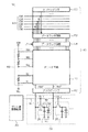
図2は、ゲート線駆動回路30の構成を示す図である。このゲート線駆動回路30は、縦続接続(カスケード接続)した複数のシフトレジスタ回路SR1,SR2,SR3,SR4・・・で構成されるシフトレジスタから成っている(説明の便宜上、縦続接続するシフトレジスタ回路SR1,SR2・・・の各々を「単位シフトレジスタ回路」と称することとし、これらを「単位シフトレジスタ回路SR」と総称する)。各単位シフトレジスタ回路SRは、1つの画素ラインすなわち1つのゲート線GLごとに設けられる。
FIG. 2 is a diagram illustrating a configuration of the gate
また図2に示すクロック発生器31は、各々位相が異なる3相のクロック信号CLK1,CLK2,CLK3をゲート線駆動回路30の単位シフトレジスタ回路SRに入力するものであり、このクロック信号CLK1,CLK2,CLK3は、表示装置の走査周期に同期したタイミングで順番に活性化するよう制御されている。
The
各単位シフトレジスタ回路SRは、入力端子IN、出力端子OUT、第1および第2クロック端子A,Bを有している。図2のように、各単位シフトレジスタ回路SRのクロック端子A,Bには、クロック発生器31が出力するクロック信号CLK1,CLK2,CLK3のうちの2つが供給される。単位シフトレジスタ回路SRの出力端子OUTには、それぞれゲート線GLが接続する。また、第1段目(第1ステージ)の単位シフトレジスタ回路SR1の入力端子INには、画像信号の各フレーム期間の先頭に対応するスタートパルスが入力信号として入力され、第2段以降の単位シフトレジスタ回路SRの入力端子INには、その前段の出力端子OUTに出力される出力信号が、入力信号として入力される。各単位シフトレジスタ回路SRの出力信号は、水平(又は垂直)走査パルスとしてゲート線GLへと出力される。
Each unit shift register SR has an input terminal IN, an output terminal OUT, and first and second clock terminals A and B. As shown in FIG. 2, two of the clock signals CLK1, CLK2, and CLK3 output from the
この構成のゲート線駆動回路30によれば、各単位シフトレジスタ回路SRは、クロック信号CLK1,CLK2,CLK3に同期して、前段から入力される入力信号(前段の出力信号)をシフトさせながら、対応するゲート線GL並びに自身の次段の単位シフトレジスタ回路SRへと出力する(単位シフトレジスタ回路SRの動作の詳細は後述する)。その結果、一連の単位シフトレジスタ回路SRは、所定の走査周期に基づいたタイミングでゲート線GLを順に活性化させる、いわゆるゲート線駆動ユニットとして機能する。
According to the gate
ここで、本発明の説明を容易にするために従来の単位シフトレジスタについて説明する。図3は、従来の単位シフトレジスタ回路SRの構成を示す回路図である。なおゲート線駆動回路30においては、縦続接続された各単位シフトレジスタ回路SRの構成は実質的にどれも同じであるので、以下では1つの単位シフトレジスタ回路SRの構成についてのみ代表的に説明する。また、この単位シフトレジスタ回路SRを構成するトランジスタは、全て同一導電型の電界効果トランジスタであるが、本実施の形態においては全てN型TFTであるものとする。
Here, in order to facilitate the description of the present invention, a conventional unit shift register will be described. FIG. 3 is a circuit diagram showing a configuration of a conventional unit shift register circuit SR. In the gate
図3の如く、従来の単位シフトレジスタ回路SRは、図2で示した入力端子IN、出力端子OUT、第1クロック端子Aおよび第2クロック端子Bの他に、低電位側電源電位VSSが供給される第1電源端子s1、高電位側電源電位VDD1,VDD2がそれぞれ供給される第2電源端子s2および第3電源端子s3を有している。高電位側電源電位VDD1,VDD2は、互いに同一レベルであってもよい。そのようにする場合には、第2電源端子s2と第3電源端子s3とを同一の端子で構成してもよい。以下の説明では、低電位側電源電位VSSが回路の基準電位となるが、実使用では画素に書込まれるデータの電圧を基準にして基準電位が設定され、例えば高電位側電源電位VDD1、VDD2は17V、低電位側電源電位VSSは−12Vなどと設定される。 As shown in FIG. 3, the conventional unit shift register circuit SR is supplied with the low-potential-side power supply potential VSS in addition to the input terminal IN, output terminal OUT, first clock terminal A, and second clock terminal B shown in FIG. The first power supply terminal s1, the second power supply terminal s2 and the third power supply terminal s3 to which the high-potential-side power supply potentials VDD1 and VDD2 are supplied, respectively. The high potential side power supply potentials VDD1 and VDD2 may be at the same level. In such a case, the second power supply terminal s2 and the third power supply terminal s3 may be configured by the same terminal. In the following description, the low-potential side power supply potential VSS is the reference potential of the circuit. However, in actual use, the reference potential is set based on the voltage of data written to the pixel. For example, the high-potential side power supply potential VDD1, VDD2 Is set to 17V, and the low-potential side power supply potential VSS is set to -12V.
単位シフトレジスタ回路SRの出力段は、出力端子OUTと第1クロック端子Aとの間に接続するトランジスタQ1(第1トランジスタ)と、出力端子OUTと第1電源端子s1との間に接続するトランジスタQ2(第2トランジスタ)とにより構成されている。以下、単位シフトレジスタ回路SRの出力段を構成するトランジスタQ1のゲート(制御電極)が接続するノードをノードN1(第1ノード)、トランジスタQ2のゲートノードをノードN2(第2ノード)と定義する。 The output stage of the unit shift register SR includes a transistor Q1 (first transistor) connected between the output terminal OUT and the first clock terminal A, and a transistor connected between the output terminal OUT and the first power supply terminal s1. Q2 (second transistor). Hereinafter, a node to which the gate (control electrode) of the transistor Q1 constituting the output stage of the unit shift register circuit SR is connected is defined as a node N1 (first node), and a gate node of the transistor Q2 is defined as a node N2 (second node). .
トランジスタQ1のゲート・ソース間(即ち出力端子OUTとノードN1との間)には昇圧容量Cが設けられている。またノードN1と第2電源端子s2との間にはトランジスタQ3が接続しており、そのゲートは入力端子INに接続している。ノードN1と第1電源端子s1との間には、トランジスタQ4並びにトランジスタQ5が接続する。トランジスタQ4のゲートは第2クロック端子Bに接続し、トランジスタQ5のゲートはノードN2に接続する。ノードN2と第3電源端子s3との間には、ダイオード接続されたトランジスタQ6が接続し、ノードN2と第1電源端子s1との間にはトランジスタQ7が接続する。トランジスタQ7のゲートはノードN1に接続する。 A boost capacitor C is provided between the gate and source of the transistor Q1 (that is, between the output terminal OUT and the node N1). A transistor Q3 is connected between the node N1 and the second power supply terminal s2, and its gate is connected to the input terminal IN. The transistor Q4 and the transistor Q5 are connected between the node N1 and the first power supply terminal s1. The gate of the transistor Q4 is connected to the second clock terminal B, and the gate of the transistor Q5 is connected to the node N2. A diode-connected transistor Q6 is connected between the node N2 and the third power supply terminal s3, and a transistor Q7 is connected between the node N2 and the first power supply terminal s1. Transistor Q7 has its gate connected to node N1.
トランジスタQ7はトランジスタQ6よりも駆動能力(電流を流す能力)が十分大きく設定されている。即ち、トランジスタQ7のオン抵抗はトランジスタQ6のオン抵抗よりも小さい。よって、トランジスタQ7のゲート電位が上昇するとノードN2の電位は下降し、トランジスタQ7のゲート電位が下降するとノードN2の電位は上昇する。即ちトランジスタQ6およびトランジスタQ7は、ノードN1を入力端としノードN2を出力端とするインバータを構成している。当該インバータは、トランジスタQ6およびトランジスタQ7のオン抵抗値の比によってその動作が規定される「レシオ型インバータ」である。当該インバータは、出力端子OUTをプルダウンさせるためにトランジスタQ2を駆動する「プルダウン駆動回路」として機能している。 The transistor Q7 is set to have a sufficiently larger driving capability (ability to flow current) than the transistor Q6. That is, the on-resistance of the transistor Q7 is smaller than the on-resistance of the transistor Q6. Therefore, when the gate potential of the transistor Q7 is increased, the potential of the node N2 is decreased, and when the gate potential of the transistor Q7 is decreased, the potential of the node N2 is increased. That is, the transistor Q6 and the transistor Q7 constitute an inverter having the node N1 as an input end and the node N2 as an output end. The inverter is a “ratio inverter” whose operation is defined by the ratio of the on-resistance values of the transistors Q6 and Q7. The inverter functions as a “pull-down drive circuit” that drives the transistor Q2 to pull down the output terminal OUT.
図3の単位シフトレジスタ回路SRの具体的な動作を説明する。ゲート線駆動回路30を構成する各単位シフトレジスタ回路SRの動作は実質的にどれも同じであるので、1つの単位シフトレジスタ回路SRの動作を代表的に説明する。簡単のため、当該単位シフトレジスタ回路SRの第1クロック端子Aにクロック信号CLK1が入力され、第2クロック端子Bにクロック信号CLK3が入力されるものとして説明を行う(例えば図2における、単位シフトレジスタ回路SR1,SR4などがこれに該当する)。また、当該単位シフトレジスタ回路SRが出力端子OUTに出力する出力信号をGn、その前段の単位シフトレジスタ回路SRの出力信号をGn-1と定義する。
A specific operation of the unit shift register circuit SR in FIG. 3 will be described. Since the operations of the unit shift register circuits SR constituting the gate
まず初期状態として、ノードN1がL(Low)レベル(VSS)、ノードN2がH(High)レベル(VDD2−Vth(Vth:トランジスタのしきい値電圧))であると仮定する(以下、この状態を「リセット状態」と称す)。また、第1クロック端子A(クロック信号CLK1)、第2クロック端子B(クロック信号CLK3)、入力端子IN(前段の出力信号Gn-1)は何れもLレベルであるとする。リセット状態では、トランジスタQ1がオフ(遮断状態)、トランジスタQ2がオン(導通状態)であるので、第1クロック端子A(クロック信号CLK1)のレベルに関係なく、出力端子OUT(出力信号Gn)はLレベルに保たれる。即ち、この単位シフトレジスタ回路SRが接続するゲート線は非選択状態にある。 First, as an initial state, it is assumed that the node N1 is at the L (Low) level (VSS) and the node N2 is at the H (High) level (VDD2-Vth (Vth: threshold voltage of the transistor)) (hereinafter, this state). Is called "Reset state"). The first clock terminal A (clock signal CLK1), the second clock terminal B (clock signal CLK3), and the input terminal IN (previous stage output signal G n-1 ) are all at L level. In the reset state, the transistor Q1 is off (cut-off state) and the transistor Q2 is on (conduction state). Therefore, regardless of the level of the first clock terminal A (clock signal CLK1), the output terminal OUT (output signal G n ). Is kept at L level. That is, the gate line connected to the unit shift register circuit SR is in a non-selected state.
その状態から、前段の単位シフトレジスタ回路SRの出力信号Gn-1がHレベルになると、それが当該単位シフトレジスタ回路SRの入力端子INに入力されトランジスタQ3がオンになる。このときノードN2はLレベルなのでトランジスタQ5もオンしているが、トランジスタQ3はトランジスタQ5よりも駆動能力が十分大きく設定されており、トランジスタQ3のオン抵抗はトランジスタQ5のオン抵抗に比べ十分低いため、ノードN1のレベルは上昇する。 From this state, when the output signal G n−1 of the previous unit shift register circuit SR becomes H level, it is input to the input terminal IN of the unit shift register circuit SR, and the transistor Q3 is turned on. At this time, since the node N2 is at the L level, the transistor Q5 is also turned on. However, the transistor Q3 is set to have a sufficiently larger driving capability than the transistor Q5, and the on-resistance of the transistor Q3 is sufficiently lower than the on-resistance of the transistor Q5. The level of the node N1 rises.
それによりトランジスタQ7が導通し始めノードN2のレベルは下降する。そうなるとトランジスタQ5の抵抗が高くなり、ノードN1のレベルが急速に上昇してトランジスタQ7を充分にオンにする。その結果ノードN2はLレベル(VSS)になり、トランジスタQ5がオフになってノードN1がHレベル(VDD1−Vth)になる。このようにノードN1がHレベル、ノードN2がLレベルの状態(以下、この状態を「セット状態」称す)では、トランジスタQ1がオン、トランジスタQ2がオフになる。なお、前段の出力信号Gn-1がLレベルに戻ってトランジスタQ3がオフしても、ノードN1はフローティング状態になるのでこのセット状態はその後も維持される。 Thereby, the transistor Q7 starts to conduct and the level of the node N2 falls. As a result, the resistance of the transistor Q5 increases, and the level of the node N1 rises rapidly to turn on the transistor Q7 sufficiently. As a result, the node N2 becomes L level (VSS), the transistor Q5 is turned off, and the node N1 becomes H level (VDD1-Vth). Thus, in a state where the node N1 is at the H level and the node N2 is at the L level (hereinafter, this state is referred to as “set state”), the transistor Q1 is turned on and the transistor Q2 is turned off. Even if the output signal G n-1 in the previous stage returns to the L level and the transistor Q3 is turned off, the node N1 is in the floating state, and this set state is maintained thereafter.
セット状態では、トランジスタQ1がオン、トランジスタQ2がオフであるので、第1クロック端子Aのクロック信号CLK1がHレベルになると、出力端子OUTのレベルが上昇する。このとき昇圧容量CおよびトランジスタQ1のゲート・チャネル間容量(ゲート容量)による結合により、ノードN1のレベルは特定の電圧(以下「昇圧量ΔV」)だけ昇圧される。そのため出力端子OUTのレベルが上昇してもトランジスタQ1のゲート・ソース間電圧はしきい値電圧(Vth)よりも大きく保たれ、当該トランジスタQ1は低インピーダンスを維持する。従って、出力信号Gnのレベルは第1クロック端子Aのレベルに追随して変化する。特に、トランジスタQ1のゲート・ソース間電圧が充分大きい場合トランジスタQ1は非飽和動作するので、しきい値電圧分の損失はなく出力端子OUTはクロック信号CLK1と同レベルになる。よって、第1クロック端子Aに入力されるクロック信号CLK1がHレベルの間は、出力信号GnもHレベルになってゲート線の選択状態になる。その後、クロック信号CLK1がLレベルに戻ると出力信号GnもLレベルになってゲート線の非選択状態に戻る。 In the set state, the transistor Q1 is on and the transistor Q2 is off. Therefore, when the clock signal CLK1 of the first clock terminal A becomes H level, the level of the output terminal OUT rises. At this time, the level of the node N1 is boosted by a specific voltage (hereinafter referred to as “boost amount ΔV”) due to the combination of the boost capacitor C and the gate-channel capacitor (gate capacitor) of the transistor Q1. Therefore, even when the level of the output terminal OUT rises, the gate-source voltage of the transistor Q1 is kept higher than the threshold voltage (Vth), and the transistor Q1 maintains a low impedance. Therefore, the level of the output signal G n changes following the level of the first clock terminal A. In particular, when the voltage between the gate and the source of the transistor Q1 is sufficiently large, the transistor Q1 operates in a non-saturated state, so there is no loss for the threshold voltage and the output terminal OUT is at the same level as the clock signal CLK1. Therefore, while the clock signal CLK1 input to the first clock terminal A is at the H level, the output signal G n is also at the H level and the gate line is selected. Thereafter, when the clock signal CLK1 returns to the L level, the output signal G n also becomes the L level and the gate line returns to the non-selected state.
その後、第2クロック端子Bのクロック信号CLK3がHレベルになると、トランジスタQ4がオンになるためノードN1がLレベルになり、それに伴ってトランジスタQ7がオフになるためノードN2はHレベルになる。即ち、トランジスタQ1がオフ、トランジスタQ2がオンのリセット状態に戻る。 Thereafter, when the clock signal CLK3 of the second clock terminal B becomes H level, the transistor Q4 is turned on, so that the node N1 becomes L level, and accordingly, the transistor Q7 is turned off, so that the node N2 becomes H level. That is, the transistor Q1 is turned off and the transistor Q2 is turned on.
以上の動作をまとめると、単位シフトレジスタ回路SRにおいては、入力端子INに信号(スタートパルスまたは前段の出力信号Gn-1)が入力されない間はリセット状態にあり、その間ノードN2がHレベル(VDD2−Vth)に保たれることで、出力端子OUT(ゲート線)は低インピーダンスのLレベル(VSS)に維持される。そして入力端子INに信号が入力されると、そのタイミングでノードN2がLレベル(VSS)になると共にノードN1がHレベル(VDD1−Vth)に充電されてセット状態になる。即ち、単位シフトレジスタ回路SRでは、入力端子INに入力される信号により、セット状態になるタイミングが規定される。 In summary, the unit shift register SR is in a reset state while no signal (start pulse or previous stage output signal G n-1 ) is input to the input terminal IN, and during that time the node N2 is at the H level ( By being maintained at (VDD2-Vth), the output terminal OUT (gate line) is maintained at a low impedance L level (VSS). When a signal is input to the input terminal IN, the node N2 becomes L level (VSS) at that timing, and the node N1 is charged to H level (VDD1-Vth) and is set. That is, in the unit shift register circuit SR, the timing to enter the set state is defined by the signal input to the input terminal IN.
セット状態では第1クロック端子Aの信号(クロック信号CLK1)がHレベルになるとノードN1の電位が昇圧量ΔVだけ高くなり、第1クロック端子AがHレベルである間、出力端子OUTがHレベルになってゲート線を活性化する(このためノードN1は「昇圧ノード」と称されることもある)。その後第2クロック端子Bに信号(クロック信号CLK3)が入力されると、ノードN1がLレベル(VSS)、ノードN2がHレベル(VDD2−Vth)に戻って、元のリセット状態になる(このためノードN2は「リセットノード」と称されることもある)。即ち、単位シフトレジスタ回路SRでは、第2クロック端子Bに入力される信号により、セット状態になるタイミングが規定される。 In the set state, when the signal of the first clock terminal A (clock signal CLK1) becomes H level, the potential of the node N1 increases by the boost amount ΔV, and the output terminal OUT is H level while the first clock terminal A is H level. Then, the gate line is activated (for this reason, the node N1 may be referred to as a “boost node”). Thereafter, when a signal (clock signal CLK3) is input to the second clock terminal B, the node N1 returns to the L level (VSS), the node N2 returns to the H level (VDD2-Vth), and the original reset state is established (this state) Therefore, the node N2 may be referred to as a “reset node”). That is, in the unit shift register circuit SR, the timing to enter the set state is defined by the signal input to the second clock terminal B.
そのように動作する複数の単位シフトレジスタ回路SRを図2のように縦続接続し、ゲート線駆動回路30を構成すると、第1段目の単位シフトレジスタ回路SR1の入力端子INに入力された入力信号(スタートパルス)は、図4に示すタイミング図のように、クロック信号CLK1,CLK2,CLK3に同期したタイミングでシフトされながら、単位シフトレジスタ回路SR2,SR3・・・と順番に伝達される。それによって、ゲート線駆動回路30は、所定の走査周期でゲート線GL1,GL2,GL3・・・を順に駆動することができる。
When a plurality of unit shift register circuits SR operating in this manner are connected in cascade as shown in FIG. 2 to form the gate
上の例では、複数の単位シフトレジスタ回路SRが3相クロックに基づいて動作する例を示したが、2相クロック信号を使用して動作させることも可能である。図5はその場合におけるゲート線駆動回路30の構成を示す図である。
In the above example, the example in which the plurality of unit shift register circuits SR operate based on the three-phase clock is shown, but it is also possible to operate using the two-phase clock signal. FIG. 5 is a diagram showing a configuration of the gate
この場合も、ゲート線駆動回路30は、縦続接続した複数の単位シフトレジスタ回路SRにより構成される。即ち、各単位シフトレジスタ回路SRの入力端子INには、その前段の単位シフトレジスタ回路SRの出力端子OUTが接続する。但し、第1段目の単位シフトレジスタ回路SRの入力端子INには、スタートパルスが入力信号として入力される。
Also in this case, the gate
この場合におけるクロック発生器31は、互いに逆相の2相クロックであるクロック信号CLK,/CLKを出力するものである。それぞれの単位シフトレジスタ回路SRの第1クロック端子Aには、隣接する単位シフトレジスタ回路SRに互いに逆相のクロック信号が入力されるよう、そのクロック信号CLK,/CLKの片方が入力される。また図5に示すように、各単位シフトレジスタ回路SRの第2クロック端子Bには、その後段(この例では次段)の単位シフトレジスタ回路SRの出力端子OUTが接続される。
In this case, the
図5のように構成されたゲート線駆動回路30における単位シフトレジスタ回路SRの動作を説明する。ここでも、1つの単位シフトレジスタ回路SRの動作を代表的に説明する。簡単のため、単位シフトレジスタ回路SRの第1クロック端子Aにクロック信号CLKが入力されるものとして説明を行う(例えば、図5における単位シフトレジスタ回路SR1,SR3などがこれに該当する)。また、当該単位シフトレジスタ回路SRの出力信号をGn、その前段および次段の単位シフトレジスタ回路SRの出力信号をそれぞれGn-1およびGn+1と定義する。
The operation of the unit shift register circuit SR in the gate
まず初期状態として、ノードN1がLレベル(VSS)、ノードN2がHレベル(VDD2−Vth)のリセット状態を仮定する。また、第1クロック端子A(クロック信号CLK)、第2クロック端子B(次段の出力信号Gn+1)、入力端子IN(前段の出力信号Gn-1)は何れもLレベルであるとする。 First, as an initial state, a reset state in which the node N1 is at the L level (VSS) and the node N2 is at the H level (VDD2-Vth) is assumed. The first clock terminal A (clock signal CLK), the second clock terminal B (next-stage output signal G n + 1 ), and the input terminal IN (previous-stage output signal G n-1 ) are all at L level. And
その状態から、前段の出力信号Gn-1がHレベルになると、それが当該単位シフトレジスタ回路SRの入力端子INに入力されトランジスタQ3がオンになり、ノードN1のレベルは上昇する。それによりトランジスタQ7が導通し始め、ノードN2のレベルは下降する。そうなるとトランジスタQ5の抵抗が高くなり、ノードN1のレベルが急速に上昇してトランジスタQ7を充分にオンにする。その結果ノードN2はLレベル(VSS)になり、トランジスタQ5がオフになってノードN1がHレベル(VDD1−Vth)になる。その結果、トランジスタQ1がオン、トランジスタQ2がオフとなるセット状態になる。 From this state, when the output signal G n-1 of the previous stage becomes H level, it is input to the input terminal IN of the unit shift register circuit SR, the transistor Q3 is turned on, and the level of the node N1 rises. As a result, transistor Q7 begins to conduct, and the level of node N2 falls. As a result, the resistance of the transistor Q5 increases, and the level of the node N1 rises rapidly to turn on the transistor Q7 sufficiently. As a result, the node N2 becomes L level (VSS), the transistor Q5 is turned off, and the node N1 becomes H level (VDD1-Vth). As a result, the transistor Q1 is turned on and the transistor Q2 is turned off.
そして、クロック信号CLKがHレベルになり出力端子OUTのレベルが上昇すると、昇圧容量CおよびトランジスタQ1のゲート・チャネル間容量による結合によりノードN1のレベルは特定の電圧(昇圧量ΔV)だけ昇圧される。従って、出力信号Gnのレベルは第1クロック端子Aのレベルに追随して変化し、クロック信号CLKがHレベルである間は出力信号GnもHレベルになる。その後、クロック信号CLKがLレベルに戻ると出力信号GnもLレベルに戻る。 When the clock signal CLK becomes H level and the level of the output terminal OUT rises, the level of the node N1 is boosted by a specific voltage (boost amount ΔV) due to the coupling by the boost capacitor C and the gate-channel capacitor of the transistor Q1. The Therefore, the level of the output signal G n changes following the level of the first clock terminal A, and the output signal G n is also at the H level while the clock signal CLK is at the H level. Thereafter, when the clock signal CLK returns to the L level, the output signal G n also returns to the L level.
出力信号Gnが次段の単位シフトレジスタ回路SRに伝達された後、次段の出力信号Gn+1がHレベルになると、それが第2クロック端子Bに入力されてトランジスタQ4がオンになりノードN1がLレベルになる。それに伴ってトランジスタQ7がオフになるのでノードN2はHレベルになる。即ち、当該単位シフトレジスタ回路SRはリセット状態に戻り、トランジスタQ1がオフ、トランジスタQ2がオンになる。 After the output signal G n is transmitted to the next unit shift register circuit SR, when the next stage output signal G n + 1 becomes H level, it is input to the second clock terminal B and the transistor Q4 is turned on. Node N1 becomes L level. Accordingly, the transistor Q7 is turned off, so that the node N2 becomes H level. That is, the unit shift register circuit SR returns to the reset state, and the transistor Q1 is turned off and the transistor Q2 is turned on.
このように、ゲート線駆動回路30が図5のように構成されている場合においても、それぞれの単位シフトレジスタ回路SRの動作は、第2クロック端子Bに入力される信号が次段の出力信号Gn+1であることを除けば図2の場合とほぼ同じである。
As described above, even when the gate
以上の動作を、図5のように縦続接続された単位シフトレジスタ回路SR1,SR2,・・・が順に行う。それによって、第1段目の単位シフトレジスタ回路SR1の入力端子INに入力された入力信号(スタートパルス)が、クロック信号CLK,/CLKに同期してシフトされながら、単位シフトレジスタ回路SR2,SR3,・・・と順番に伝達される。その結果、ゲート線駆動回路30は図6に示すタイミング図の如く、クロック信号CLK,/CLKに同期して、ゲート線GL1,GL2,GL3,・・・を順に駆動することができる。
The above operations are sequentially performed by the unit shift register circuits SR1, SR2,... Connected in cascade as shown in FIG. Thereby, the input signal (start pulse) input to the input terminal IN of the first stage unit shift register circuit SR1 is shifted in synchronization with the clock signals CLK, / CLK, while the unit shift register circuits SR2, SR3. , ... in order. As a result, the gate
但し、図5の構成では、各単位シフトレジスタ回路SRは、第2クロック端子Bに次段の単位シフトレジスタ回路SRの出力信号Gn+1が入力されるので、次段の単位シフトレジスタ回路SRが少なくとも一度動作した後でなければリセット状態(すなわち上記の初期状態)にならない。各単位シフトレジスタ回路SRは、リセット状態を経なければ図6に示したような通常動作を行うことができない。従って図5の構成の場合には、通常動作に先立って、ダミーの入力信号を単位シフトレジスタ回路SRの第1段目から最終段まで伝達させるダミー動作を行わせる必要がある。あるいは、各単位シフトレジスタ回路SRのノードN2と第3電源端子s3(高電位側電源)との間にリセット用のトランジスタを別途設け、通常動作の前に強制的にノードN2を充電するリセット動作を行なってもよい。但し、その場合はリセット用の信号ラインが別途必要になる。 However, in the configuration of FIG. 5, each unit shift register circuit SR receives the output signal G n + 1 of the next stage unit shift register circuit SR to the second clock terminal B, so that the next stage unit shift register circuit The reset state (i.e., the above-described initial state) is not made until after the SR has been operated at least once. Each unit shift register circuit SR cannot perform the normal operation as shown in FIG. 6 without passing through the reset state. Therefore, in the configuration of FIG. 5, it is necessary to perform a dummy operation for transmitting a dummy input signal from the first stage to the last stage of the unit shift register circuit SR prior to the normal operation. Alternatively, a reset transistor is separately provided between the node N2 of each unit shift register circuit SR and the third power supply terminal s3 (high potential side power supply) to forcibly charge the node N2 before the normal operation. May be performed. In this case, however, a reset signal line is required separately.
ここで、先に述べた従来の単位シフトレジスタ回路SRにおける誤動作の問題を詳細に説明する。以下では、単位シフトレジスタ回路SRを構成する各トランジスタはa−Si TFTであるとする。 Here, the problem of malfunction in the above-described conventional unit shift register circuit SR will be described in detail. Hereinafter, it is assumed that each transistor constituting the unit shift register circuit SR is an a-Si TFT.
図6の最下段に、図5のゲート線駆動回路30における単位シフトレジスタ回路SR1のノードN2の電圧波形を示す。上記のように、入力端子INの信号(スタートパルスあるいは前段の出力信号Gn-1)がHレベルに成ると、ノードN2はLレベルに遷移するが、すぐに第2クロック端子Bの信号(次段の出力信号Gn+1)によってHレベルに戻され、その後約1フレーム期間(約16ms)Hレベルに維持される(図示は省略するが、この振る舞いは図2のケースでも同様である)。つまり各単位シフトレジスタ回路SRにおける、トランジスタQ2およびトランジスタQ5のゲートは、約1フレーム期間継続的(直流的)に正バイアスされる。よって単位シフトレジスタ回路SRがa−Si TFTにより構成されている場合には、トランジスタQ2,Q5はしきい値電圧が正方向にシフトして駆動能力が低下する。
6 shows a voltage waveform at the node N2 of the unit shift register circuit SR1 in the gate
単位シフトレジスタ回路SRがゲート線の非選択期間にあり、リセット状態(ノードN1がLレベル、ノードN2がHレベル)になっている場合を想定する。この状態ではトランジスタQ1はオフしているが、そのドレインが接続する第1クロック端子Aにはクロック信号CLKが繰り返し入力される。 Assume that the unit shift register SR is in a gate line non-selection period and is in a reset state (node N1 is at L level and node N2 is at H level). In this state, the transistor Q1 is off, but the clock signal CLK is repeatedly input to the first clock terminal A to which the drain is connected.
このときトランジスタQ1のドレインとゲートとの間のオーバラップ容量による結合により、クロック信号CLKの入力に伴ってノードN1の電圧が変動する。すなわちクロック信号CLKの立上り時にノードN1が充電され、その後トランジスタQ5を介して放電されという振る舞いが繰り返し行われる。従ってノードN1には、鋸歯状の繰り返し波形のノイズが生じる。当該ノイズによりトランジスタQ7がオンすると、ノードN2のレベルが下降してしまう。 At this time, due to the coupling due to the overlap capacitance between the drain and gate of the transistor Q1, the voltage at the node N1 varies with the input of the clock signal CLK. That is, the behavior that the node N1 is charged at the rising edge of the clock signal CLK and then discharged through the transistor Q5 is repeated. Therefore, sawtooth-like repetitive waveform noise is generated at the node N1. When the transistor Q7 is turned on by the noise, the level of the node N2 falls.
上記のように単位シフトレジスタ回路SRのトランジスタQ2,Q5のゲート・ソース間は直流的に正バイアスされるため、当該トランジスタQ2,Q5は駆動能力が時間と共に低下する。そのような状態でノードN2のレベルが低下すると、トランジスタQ5はノードN1のノイズによる電荷を素早く放電することができず、ノードN1のレベルがさらに上昇する。応じてトランジスタQ1の抵抗値が下がるため、クロック信号CLKがHレベルになったときに出力端子OUTに電荷が供給されるようになる。またこのときトランジスタQ2の駆動能力も低下しているため、トランジスタQ2は出力端子OUTの電荷を素早く放電できず、出力端子OUTのレベルが上昇してしまう。つまり、非選択状態にあるべきゲート線が選択状態になってしまうという誤動作が生じ、液晶表示装置10の表示不具合が発生する。以下、この問題を解決可能な本発明に係るシフトレジスタ回路について説明する。
As described above, since the gate and source of the transistors Q2 and Q5 of the unit shift register circuit SR are positively biased in a direct current manner, the driving capability of the transistors Q2 and Q5 decreases with time. When the level of the node N2 decreases in such a state, the transistor Q5 cannot quickly discharge the charge due to the noise of the node N1, and the level of the node N1 further increases. Accordingly, the resistance value of the transistor Q1 decreases, so that charge is supplied to the output terminal OUT when the clock signal CLK becomes H level. At this time, since the driving capability of the transistor Q2 is also reduced, the transistor Q2 cannot quickly discharge the charge of the output terminal OUT, and the level of the output terminal OUT rises. That is, a malfunction occurs in which a gate line that should be in a non-selected state is in a selected state, causing a display defect of the liquid
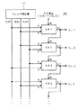
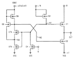
図7は、実施の形態1に係る単位シフトレジスタ回路SRの構成を示す回路図である。同図のように、当該単位シフトレジスタ回路SRの出力段は、出力端子OUTと第1クロック端子Aとの間に接続するトランジスタQ1(第1トランジスタ)と、出力端子OUTと第1電源端子s1との間に接続するトランジスタQ2(第2トランジスタ)とにより構成されている。また、トランジスタQ1のゲート(制御電極)とソースとの間すなわちノードN1と出力端子OUTとの間には昇圧容量Cが設けられている。ノードN1と第2電源端子s2との間には、ゲートが入力端子INに接続するトランジスタQ3が接続しており、ノードN1と第1電源端子s1との間には、ゲートが第2クロック端子Bに接続するトランジスタQ4と、ゲートがノードN2に接続したトランジスタQ5とが接続している。以上の構成は図3に示した従来の単位シフトレジスタ回路SRと同様である。 FIG. 7 is a circuit diagram showing a configuration of the unit shift register circuit SR according to the first embodiment. As shown in the figure, the output stage of the unit shift register circuit SR includes a transistor Q1 (first transistor) connected between the output terminal OUT and the first clock terminal A, the output terminal OUT, and the first power supply terminal s1. And a transistor Q2 (second transistor) connected between them. A boosting capacitor C is provided between the gate (control electrode) and source of the transistor Q1, that is, between the node N1 and the output terminal OUT. A transistor Q3 whose gate is connected to the input terminal IN is connected between the node N1 and the second power supply terminal s2. The gate is connected to the second clock terminal between the node N1 and the first power supply terminal s1. The transistor Q4 connected to B and the transistor Q5 whose gate is connected to the node N2 are connected. The above configuration is the same as that of the conventional unit shift register SR shown in FIG.
本実施の形態に係る単位シフトレジスタ回路SRも、ノードN1を入力端としノードN2を出力端とするインバータ(第1プルダウン駆動回路)を備えている。本実施の形態においては、当該インバータはトランジスタQ6,Q7A,Q7B,Q8により構成される。図7の如く、トランジスタQ6はダイオード接続されており、ノードN2と第3電源端子s3との間に接続している。トランジスタQ7A,Q7BはノードN2と第1電源端子s1との間に直列に接続し、それぞれのゲートはノードN1に接続している。またトランジスタQ7AとトランジスタQ7Bとの接続ノードをN3と定義すると、トランジスタQ8は当該ノードN3と高電位側電源電位VDD3が供給される第4電源端子s4との間に接続されており、そのゲートはノードN2に接続している。トランジスタQ8は、ノードN2の電位で制御されて、第4電源端子s4からノードN3へ帰還電流を流すよう機能する。以上のような構成のインバータは「シュミット・トリガ回路」と呼ばれることもある(例えば特開昭56−96525号公報参照)。 The unit shift register SR according to the present embodiment also includes an inverter (first pull-down drive circuit) having the node N1 as an input terminal and the node N2 as an output terminal. In the present embodiment, the inverter includes transistors Q6, Q7A, Q7B, and Q8. As shown in FIG. 7, the transistor Q6 is diode-connected and is connected between the node N2 and the third power supply terminal s3. The transistors Q7A and Q7B are connected in series between the node N2 and the first power supply terminal s1, and each gate is connected to the node N1. If a connection node between the transistor Q7A and the transistor Q7B is defined as N3, the transistor Q8 is connected between the node N3 and the fourth power supply terminal s4 to which the high potential side power supply potential VDD3 is supplied, and its gate is Connected to node N2. The transistor Q8 is controlled by the potential of the node N2, and functions to flow a feedback current from the fourth power supply terminal s4 to the node N3. The inverter having the above configuration is sometimes called a “Schmitt trigger circuit” (see, for example, Japanese Patent Laid-Open No. 56-96525).
高電位側電源電位VDD3は、ノードN2がHレベルとなってトランジスタQ8がオンしたときにノードN3を所定のレベルに充電することが可能な電位であり、例えば高電位側電源電位VDD1,VDD2と同一レベルであってもよい。例えば高電位側電源電位VDD3を高電位側電源電位VDD2と同一レベルとする場合には、図8に示すが如く、第3電源端子s3と第4電源端子s4とを互いに接続し、両者を同一の端子で構成してもよい(即ち、第3電源端子s3を第4電源端子s4としても機能させる)。そのようにすることで、電源供給のための配線の占有面積は削減される。説明の簡単のため、以下においては図8の回路構成に基づいて説明を行う。 The high-potential side power supply potential VDD3 is a potential that can charge the node N3 to a predetermined level when the node N2 becomes H level and the transistor Q8 is turned on. For example, the high-potential side power supply potential VDD1 and VDD2 It may be the same level. For example, when the high potential side power supply potential VDD3 is set to the same level as the high potential side power supply potential VDD2, as shown in FIG. 8, the third power supply terminal s3 and the fourth power supply terminal s4 are connected to each other, and both are the same. (That is, the third power supply terminal s3 also functions as the fourth power supply terminal s4). By doing so, the occupation area of the wiring for power supply is reduced. For the sake of simplicity, the following description is based on the circuit configuration of FIG.
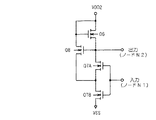
図3と図8とを比較して分かるように、従来の単位シフトレジスタ回路SRが備えるプルダウン駆動回路は図9に示すインバータであり、本実施の形態に係るプルダウン駆動回路は図10に示すインバータである。本実施の形態に係る単位シフトレジスタ回路SRは、このインバータの回路構成が従来のものと異なっているものの、論理的な動作は先に図4あるいは図6を用いて説明した従来のものと同様である。従って、本実施の形態に係る単位シフトレジスタ回路SRの動作についての説明は省略する。 As can be seen by comparing FIG. 3 and FIG. 8, the pull-down drive circuit provided in the conventional unit shift register circuit SR is the inverter shown in FIG. 9, and the pull-down drive circuit according to the present embodiment is the inverter shown in FIG. It is. Although the unit shift register circuit SR according to the present embodiment is different in the circuit configuration of the inverter from the conventional one, the logical operation is the same as that of the conventional one described with reference to FIG. 4 or FIG. It is. Therefore, the description of the operation of the unit shift register SR according to the present embodiment is omitted.
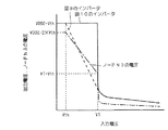
図11は、図9および図10に示したインバータの入出力電圧特性を示すグラフである。図11のように、図9のインバータでは入力電圧が駆動トランジスタQ7のしきい値電圧Vthを越えると当該トランジスタQ7が導通し始めて出力電圧が下降し始めるが、図10のインバータでは、従来のインバータに比べ出カレベルが下降を始める電圧(インバータのしきい値電圧=VT)がそれよりも高い。 FIG. 11 is a graph showing input / output voltage characteristics of the inverter shown in FIGS. 9 and 10. As shown in FIG. 11, when the input voltage exceeds the threshold voltage Vth of the drive transistor Q7 in the inverter of FIG. 9, the transistor Q7 starts to conduct and the output voltage starts to drop. However, in the inverter of FIG. Compared to the above, the voltage at which the output level starts to decrease (the threshold voltage of the inverter = VT) is higher than that.
図10のインバータでは、入力電圧がLレベル、出力電圧がHレベルであるときはトランジスタQ8がオンになるので、トランジスタQ7Aのソース(ノードN3)は正バイアスされる。トランジスタQ7Aはゲートの電位がソースの電位よりもしきい値Vth以上高くならなければ導通しないので、図10のインバータを反転させるためには、入力電位(ノードN1の電位)がバイアスされたノードN3の電位よりもさらにしきい値電圧Vth以上高くなる必要がある。従って上記のように、図10のインバータのしきい値電圧が、図9のインバータのそれよりも高いことになる。 In the inverter of FIG. 10, when the input voltage is L level and the output voltage is H level, the transistor Q8 is turned on, so that the source (node N3) of the transistor Q7A is positively biased. Since the transistor Q7A is not turned on unless the gate potential is higher than the source potential by the threshold Vth or more, in order to invert the inverter of FIG. 10, the input potential (the potential of the node N1) of the node N3 to which the input potential (the potential of the node N1) is biased. The threshold voltage Vth must be higher than the potential. Therefore, as described above, the threshold voltage of the inverter of FIG. 10 is higher than that of the inverter of FIG.
図10のインバータの動作原理を説明する。まず、入力電圧がLレベルとであるとする。その状態では、トランジスタQ7A,Q7Bがオフであるので出力電圧はHレベル(VDD2−Vth)である。そのためトランジスタQ8はオンしており、ノードN3はVDD−2×Vthのレベルにバイアスされている。 The operating principle of the inverter of FIG. 10 will be described. First, it is assumed that the input voltage is L level. In this state, the transistors Q7A and Q7B are off, so that the output voltage is at the H level (VDD2-Vth). Therefore, the transistor Q8 is on, and the node N3 is biased to the level of VDD-2 × Vth.
そして入力レベルが上昇し始めトランジスタQ7Bのしきい値電圧(Vth)を超えると、トランジスタQ7Aが導通し始めノードN3のレベルが低下するが、トランジスタQ7Aは入力レベルがノードN3の電位よりもVth以上高くならなければ導通しないので、それまではHレベルは維持される。そしてさらに入力電圧が上昇してついにノードN3の電位よりもVth以上高くなると、トランジスタQ7Aが導通し始める。 When the input level begins to rise and exceeds the threshold voltage (Vth) of transistor Q7B, transistor Q7A begins to conduct and the level at node N3 decreases, but transistor Q7A has an input level Vth higher than the potential at node N3. Since it does not conduct unless it becomes high, the H level is maintained until then. When the input voltage further rises and finally becomes higher than the potential of the node N3 by Vth or more, the transistor Q7A starts to conduct.
すると当該インバータ内で、トランジスタQ7Aの駆動能力上昇→出力電圧のレベル低下→トランジスタQ8の駆動能力低下→ノードN3のレベル低下→トランジスタQ7Aの駆動能力上昇→・・・という正帰還ループが構成され、図11のグラフのように急激に反転する。 Then, in the inverter, a positive feedback loop is formed in which the driving capability of the transistor Q7A is increased, the output voltage level is decreased, the driving capability of the transistor Q8 is decreased, the level of the node N3 is decreased, the driving capability of the transistor Q7A is increased, and so on. As shown in the graph of FIG.
また、入力電圧がHレベルの状態から下降するときは、入力電圧がインバータのしきい値電圧VTにまで下がると、トランジスタQ7Aの駆動能力低下→出力電圧のレベル上昇→トランジスタQ8の駆動能力上昇→ノードN3のレベル上昇→トランジスタQ7Aの駆動能力低下→・・・という上記と逆のループが構成されて、この場合にも急激に反転する。 When the input voltage decreases from the H level, when the input voltage decreases to the threshold voltage VT of the inverter, the drive capability of the transistor Q7A decreases → the output voltage level increases → the drive capability of the transistor Q8 increases → A loop opposite to the above is formed in which the level of the node N3 rises, the drive capability of the transistor Q7A falls, and so on.
以上のように、図10のインバータは、図9のインバータに比較してしきい値電圧が高い。よって図10のインバータがプルダウン駆動回路として用いられている本実施の形態に係る単位シフトレジスタ回路SRにおいては、ノードN1がLレベルであるリセット状態に当該レベルがある程度変動したとしても、ノードN2のレベル低下が生じ難い。よって、トランジスタQ1がオフの期間に、オーバラップ容量に起因するノイズがノードN1に生じてもノードN2のレベル低下は防止される。従って、リセット状態におけるノードN1のノイズによる誤動作の問題を解決することができる。その結果、本実施の形態に係る単位シフトレジスタ回路SRにより構成されたゲート線駆動回路を有する表示装置における表示不具合を防止できる。 As described above, the inverter of FIG. 10 has a higher threshold voltage than the inverter of FIG. Therefore, in the unit shift register SR according to the present embodiment in which the inverter of FIG. 10 is used as a pull-down drive circuit, even if the level changes to some extent in the reset state in which the node N1 is at the L level, The level is unlikely to decrease. Therefore, even when noise due to the overlap capacitance is generated at the node N1 during the period when the transistor Q1 is off, the level decrease of the node N2 is prevented. Therefore, it is possible to solve the problem of malfunction due to the noise of the node N1 in the reset state. As a result, it is possible to prevent display defects in the display device having the gate line driving circuit constituted by the unit shift register circuit SR according to the present embodiment.
特に、単位シフトレジスタ回路SRがa−Si TFTで構成されている場合には、ゲートがノードN2に接続したトランジスタQ2,Q5の駆動能力が低下して上記の誤動作の問題が生じやすくなるため、本発明の適用は効果的である。 In particular, when the unit shift register circuit SR is composed of an a-Si TFT, the drive capability of the transistors Q2 and Q5 whose gates are connected to the node N2 is reduced, and the above malfunction problem is likely to occur. The application of the present invention is effective.
<実施の形態2>
図12は、本発明の実施の形態2に係る単位シフトレジスタ回路SRの構成を示す回路図である。本実施の形態では、トランジスタQ3のドレインを電源ではなく入力端子INに接続させる。それにより電源供給のための配線の占有面積を削減できる。但し、入力端子INにはその前段の出力端子OUTが接続するため、各単位シフトレジスタ回路SRの出力段への負荷が大きくなるので、回路動作の速度が劣化する場合もあることに留意すべきである。
<
FIG. 12 is a circuit diagram showing a configuration of a unit shift register circuit SR according to the second embodiment of the present invention. In this embodiment, the drain of the transistor Q3 is connected to the input terminal IN instead of the power supply. Thereby, the area occupied by the wiring for supplying power can be reduced. However, it should be noted that since the output terminal OUT of the previous stage is connected to the input terminal IN, the load on the output stage of each unit shift register circuit SR becomes large, so that the circuit operation speed may be deteriorated. It is.
<実施の形態3>
TFTを含む電界効果トランジスタは、ゲートにしきい値電圧以上の電圧が印加されたときに、ゲート絶縁膜を介したゲート電極の直下に形成される導電性チャネルによりドレイン・ソース間が電気的に接続されることにより導通する素子である。従って、導通状態の電界効果トランジスタは、ゲートとチャネルを両電極とし、ゲート絶縁膜を誘電体層とする容量素子(ゲート容量)としても機能することができる。
<
In a field effect transistor including a TFT, when a voltage higher than a threshold voltage is applied to the gate, the drain and the source are electrically connected by a conductive channel formed immediately below the gate electrode through the gate insulating film. It is an element which conducts by being conducted. Accordingly, the conductive field effect transistor can also function as a capacitor element (gate capacitor) having both the gate and channel as electrodes and the gate insulating film as a dielectric layer.
図13は実施の形態3に係る単位シフトレジスタ回路SRの構成を示す回路図である。実施の形態1では、ノードN1の昇圧を効率よく行うためにトランジスタQ1のドレイン・ソース間に昇圧容量Cを設けていたが、本実施の形態ではそれをトランジスタQ1のゲート容量に置き換えている。その場合、図13の回路図の如く昇圧容量Cは不要になる。 FIG. 13 is a circuit diagram showing a configuration of a unit shift register circuit SR according to the third embodiment. In the first embodiment, the booster capacitor C is provided between the drain and source of the transistor Q1 in order to efficiently boost the node N1, but in the present embodiment, it is replaced with the gate capacitor of the transistor Q1. In that case, the step-up capacitor C is unnecessary as shown in the circuit diagram of FIG.
通常、半導体集積回路内に形成される容量素子の誘電体層となる絶縁膜の厚さは、トランジスタのゲート絶縁膜の厚さと同じになるので、容量素子をトランジスタのゲート容量に置き換える場合には、その容量素子と同一面積のトランジスタで代替することができる。即ち、図13においてトランジスタQ1のゲート幅を相当分広くすることで、実施の形態1に係る図8の回路と同等の昇圧動作を実現できる。またトランジスタQ1のゲート幅を広くすることによりその駆動能力が高くなるので、結果として出力信号の立上りおよび立下り速度が速くなり、動作の高速化を図ることができるという利点もある。 Usually, the thickness of the insulating film that becomes the dielectric layer of the capacitive element formed in the semiconductor integrated circuit is the same as the thickness of the gate insulating film of the transistor. Therefore, when replacing the capacitive element with the gate capacitance of the transistor, A transistor having the same area as the capacitor element can be substituted. That is, in FIG. 13, the boosting operation equivalent to the circuit of FIG. 8 according to the first embodiment can be realized by considerably widening the gate width of the transistor Q1. Further, since the driving capability is increased by widening the gate width of the transistor Q1, as a result, the rising and falling speeds of the output signal are increased, and there is an advantage that the operation can be speeded up.
<実施の形態4>
例えば図3に示した従来の単位シフトレジスタ回路SRにおいて、ノードN1と第1電源端子s1(低電位側電源電位VSS)との間には、トランジスタQ4,Q5の2つが接続している。そのうちトランジスタQ4は主に、HレベルにあるノードN1の電荷を放電してLレベルに遷移させる働きをしており、トランジスタQ5は主に、LレベルになったノードN1を低電位側電源電位VSSに固定する働きをしている。
<
For example, in the conventional unit shift register SR shown in FIG. 3, two transistors Q4 and Q5 are connected between the node N1 and the first power supply terminal s1 (low potential side power supply potential VSS). Among them, the transistor Q4 mainly functions to discharge the charge of the node N1 at the H level and make a transition to the L level, and the transistor Q5 mainly applies the node N1 at the L level to the low potential side power supply potential VSS. It works to fix.
仮に従来の単位シフトレジスタ回路SRからトランジスタQ5が省略されたとしても、Lレベルになった後のノードN1がフローティング状態になるだけであるので、理論的な動作は可能である。トランジスタQ5を省略すればそれだけ装置の縮小化を図ることができるという利点があるため、トランジスタQ5を有していない構造のレベルシフト回路も提案されている(上記の特許文献2)。 Even if the transistor Q5 is omitted from the conventional unit shift register SR, a theoretical operation is possible because the node N1 after the L level is only in a floating state. If the transistor Q5 is omitted, there is an advantage that the size of the device can be reduced. Therefore, a level shift circuit having a structure without the transistor Q5 has also been proposed (Patent Document 2).
但し、トランジスタQ5はLレベルにあるノードN1のノイズの放電経路になるため、それが省略されるとトランジスタQ1のオーバラップ容量に起因するノイズの影響が大きくなり、それによる誤動作の問題が顕著になる。そこで本実施の形態では、本発明をトランジスタQ5を有さない構造の単位シフトレジスタ回路SRへ適用することによって、その問題を解決する。 However, since the transistor Q5 becomes a noise discharge path of the node N1 at the L level, if it is omitted, the influence of noise due to the overlap capacitance of the transistor Q1 becomes large, and the problem of malfunction due to this becomes remarkable. Become. Therefore, in this embodiment, the problem is solved by applying the present invention to the unit shift register circuit SR having the structure without the transistor Q5.
図14は、実施の形態4に係る単位シフトレジスタ回路SRの構成を示す回路図である。同図の如く、当該単位シフトレジスタ回路SRは、図8の回路に対して、トランジスタQ5が省略された構造を有している。また実施の形態2が適用されており、トランジスタQ3のドレインを入力端子INに接続させ、電源供給のための配線の占有面積を削減を図っている。さらに実施の形態3が適用されており、昇圧容量Cも省略されている。 FIG. 14 is a circuit diagram showing a configuration of a unit shift register circuit SR according to the fourth embodiment. As shown in the figure, the unit shift register SR has a structure in which the transistor Q5 is omitted from the circuit of FIG. In addition, the second embodiment is applied, and the drain of the transistor Q3 is connected to the input terminal IN to reduce the area occupied by the wiring for supplying power. Further, the third embodiment is applied, and the boost capacitor C is also omitted.
上記のようにトランジスタQ5はLレベルにあるノードN1のノイズの放電経路であったため、図14のようにそれを有さない単位シフトレジスタ回路SRでは、トランジスタQ1のオーバラップ容量に起因するノイズにより、リセット状態でのノードN1のレベル変動が大きくなりやすい。しかし図14の単位シフトレジスタ回路SRでは、ノードN1を入力端としノードN2を出力端とするインバータ(プルダウン駆動回路)がトランジスタQ6,Q7A,Q7B,Q8によって図10のように構成されており、そのしきい値電圧が高い。従って当該インバータはリセット状態におけるノードN1のノイズの影響を受けにくく、当該ノイズによる誤動作は防止される。このように本発明はトランジスタQ5を有さない構造の単位シフトレジスタ回路SRに対して特に効果的である。 As described above, the transistor Q5 is a noise discharge path of the node N1 at the L level. Therefore, in the unit shift register circuit SR without the transistor Q5 as shown in FIG. 14, due to noise caused by the overlap capacitance of the transistor Q1. The level fluctuation of the node N1 in the reset state is likely to increase. However, in the unit shift register circuit SR of FIG. 14, an inverter (pull-down drive circuit) having the node N1 as an input terminal and the node N2 as an output terminal is configured by transistors Q6, Q7A, Q7B, and Q8 as shown in FIG. The threshold voltage is high. Therefore, the inverter is not easily affected by the noise of the node N1 in the reset state, and malfunction due to the noise is prevented. As described above, the present invention is particularly effective for the unit shift register circuit SR having the structure without the transistor Q5.
また図14のように、トランジスタQ5を省略すると共に、実施の形態2を適用して電源配線を省略し、さらに実施の形態3を適用して昇圧容量Cを省略すれば、単位シフトレジスタ回路SRの形成面積をより小さくすることができ表示装置の小型化に効果的である。 As shown in FIG. 14, when the transistor Q5 is omitted, the power supply wiring is omitted by applying the second embodiment, and the boosting capacitor C is omitted by applying the third embodiment, the unit shift register circuit SR. It is possible to reduce the formation area of the display device, which is effective for downsizing the display device.
<実施の形態5>
例えば図3に示した従来の単位シフトレジスタ回路SRにおいて、入力端子INへの入力信号(スタートパルスまたは前段の出力信号Gn-1)がHレベルになる直前はリセット状態であるのでトランジスタQ5はオン状態にある。
<Embodiment 5>
For example, in the conventional unit shift register SR shown in FIG. 3, the transistor Q5 is in the reset state immediately before the input signal to the input terminal IN (the start pulse or the previous stage output signal G n-1 ) becomes H level. It is on.
従って先に述べたように、入力端子INがHレベルになり単位シフトレジスタ回路SRがリセット状態からセット状態へ移行する際には、次のような段階が踏まれる。即ち、入力端子INがHレベルになると、トランジスタQ3とトランジスタQ5のオン抵抗の比に応じてノードN1のレベルが上昇し、それによりトランジスタQ7が導通し始めノードN2のレベルを下降させる。それにより、トランジスタQ5の抵抗がさらに高くなってノードN1のレベルがさらに上昇し、トランジスタQ7が充分にオンになってノードN2がLレベル(VSS)になる。応じてトランジスタQ5がオフになるのでノードN1はHレベル(VDD1−Vth)になる。その結果単位シフトレジスタ回路SRはセット状態になる。 Therefore, as described above, when the input terminal IN becomes H level and the unit shift register circuit SR shifts from the reset state to the set state, the following steps are taken. That is, when the input terminal IN becomes H level, the level of the node N1 increases according to the ratio of the on-resistances of the transistors Q3 and Q5, whereby the transistor Q7 starts to conduct and the level of the node N2 decreases. Accordingly, the resistance of the transistor Q5 is further increased, and the level of the node N1 is further increased, the transistor Q7 is sufficiently turned on, and the node N2 is set to the L level (VSS). Accordingly, since the transistor Q5 is turned off, the node N1 becomes H level (VDD1-Vth). As a result, the unit shift register circuit SR is set.
単位シフトレジスタ回路SRでは、リセット状態からセット状態へ切り替わる際に以上の動作を経るため、その切り替わりに比較的長い時間を要していた。そのことは単位シフトレジスタ回路SRの動作の高速化の妨げとなり、ひいては単位シフトレジスタ回路SRをゲート線駆動回路に用いた表示装置の高解像度化の妨げとなる。 In the unit shift register SR, since the above operation is performed when switching from the reset state to the set state, a relatively long time is required for the switching. This hinders the speeding up of the operation of the unit shift register circuit SR, and consequently hinders the increase in the resolution of the display device using the unit shift register circuit SR as the gate line driving circuit.
その対策としては、例えば図15に示すようにノードN2と第1電源端子s1(低電位側電源電位VSS)との間に、ゲートが入力端子INに接続したトランジスタQ9を設けることが考えられる。図15の回路によれば、入力端子INがHレベルになったときにトランジスタQ9がオンして、ノードN2を瞬時にLレベルなる。またそれに応じてトランジスタQ5がオフになるので、ノードN1のレベルは高速にHレベルになる。即ち、リセット状態からセット状態への切り替わりが瞬時に行われるため、単位シフトレジスタ回路SRの動作の高速化に寄与できる。 As a countermeasure, for example, as shown in FIG. 15, a transistor Q9 having a gate connected to the input terminal IN may be provided between the node N2 and the first power supply terminal s1 (low-potential-side power supply potential VSS). According to the circuit of FIG. 15, the transistor Q9 is turned on when the input terminal IN becomes H level, and the node N2 is instantaneously set to L level. Further, since the transistor Q5 is turned off accordingly, the level of the node N1 becomes H level at high speed. That is, since the switching from the reset state to the set state is instantaneously performed, it is possible to contribute to speeding up the operation of the unit shift register circuit SR.
しかし、図15の単位シフトレジスタ回路SRがゲート線駆動回路回路に用いられた場合には、次のような問題が生じる。即ち、ゲート線は多数のデータ線(図1のデータ線DL1,DL2・・・)と交叉しているため、データ線との間の寄生容量による結合によって、データ線へのデータの書込み時、あるいは対向電極(図1の共通電極ノードNC)の極性反転時において、ゲート線にノイズが加わりやすい。単位シフトレジスタ回路SRがリセット状態のときに、そのノイズがゲート線を介して入力端子INに加わると、トランジスタQ9に電流が流れてノードN2のLレベルを低下させる。 However, when the unit shift register SR shown in FIG. 15 is used in a gate line driving circuit, the following problem occurs. That is, since the gate line intersects with a large number of data lines (data lines DL1, DL2,... In FIG. 1), when data is written to the data lines due to coupling with the data lines due to parasitic capacitance, Alternatively, when the polarity of the counter electrode (common electrode node NC in FIG. 1) is reversed, noise is easily added to the gate line. When the unit shift register SR is in the reset state, if the noise is applied to the input terminal IN via the gate line, a current flows through the transistor Q9 to lower the L level of the node N2.
その結果、トランジスタQ2,Q5は駆動能力が低下するため、単位シフトレジスタ回路SRが、トランジスタQ1のオーバラップ容量に起因するノードN1のノイズの影響を受けやすくなり、実施の形態1で説明した従来のレベルシフト回路の誤動作と同様の問題が生じる。特に単位シフトレジスタ回路SRがa−Si TFTにより構成されている場合には、トランジスタQ2,Q5は駆動能力は時間と共にさらに低下するため、その問題は顕著になる。本実施の形態では、この問題を解決することが可能な単位シフトレジスタ回路SRを提案する。 As a result, since the driving capabilities of the transistors Q2 and Q5 are reduced, the unit shift register circuit SR is likely to be affected by the noise of the node N1 due to the overlap capacitance of the transistor Q1, and the conventional one explained in the first embodiment. This causes the same problem as the malfunction of the level shift circuit. In particular, when the unit shift register circuit SR is formed of an a-Si TFT, the driving capability of the transistors Q2 and Q5 further decreases with time, and the problem becomes remarkable. In the present embodiment, a unit shift register SR that can solve this problem is proposed.
再び図15の回路を参照し、トランジスタQ6およびトランジスタQ9に着目すると、それらは入力端子INを入力端としノードN2を出力端とする、図9に示したインバータを構成している。入力端子INに加わるノイズにより、ノードN2のレベルが下がるという上記の問題は、このインバータがノイズにの影響を受けやすいことが原因となっている。 Referring to the circuit of FIG. 15 again, paying attention to the transistors Q6 and Q9, they constitute the inverter shown in FIG. 9 having the input terminal IN as an input terminal and the node N2 as an output terminal. The above problem that the level of the node N2 is lowered due to noise applied to the input terminal IN is caused by the fact that this inverter is easily affected by noise.
図16は、実施の形態5に係る単位シフトレジスタ回路SRの構成を示す回路図である。同図の如く、当該単位シフトレジスタ回路SRは、ノードN2と第1電源端子s1との間に直列に接続し、共にゲートが入力端子INに接続したトランジスタQ9A,Q9Bを有している。またトランジスタQ9AとトランジスタQ9Bとの接続ノードをノードN4と定義すると、トランジスタQ8は当該ノードN4と第3電源端子s3との間に接続されており、そのゲートはノードN2に接続する。つまり本実施の形態のトランジスタQ8は、ノードN2の電位で制御されて、第3電源端子s3からノードN4へ帰還電流を流すよう機能する。従って、トランジスタQ6,Q8,Q9A,Q9Bによって、いわゆる「シュミット・トリガ回路」が構成されている。 FIG. 16 is a circuit diagram showing a configuration of a unit shift register circuit SR according to the fifth embodiment. As shown in the figure, the unit shift register SR has transistors Q9A and Q9B connected in series between the node N2 and the first power supply terminal s1, and both gates connected to the input terminal IN. When a connection node between the transistor Q9A and the transistor Q9B is defined as a node N4, the transistor Q8 is connected between the node N4 and the third power supply terminal s3, and its gate is connected to the node N2. That is, the transistor Q8 in this embodiment is controlled by the potential of the node N2 and functions to flow a feedback current from the third power supply terminal s3 to the node N4. Therefore, the transistors Q6, Q8, Q9A, and Q9B constitute a so-called “Schmitt trigger circuit”.
即ち、図16の単位シフトレジスタ回路SRは、トランジスタQ6,Q7から成り、ノードN1の入力端にしノードN2を出力端にする第1のインバータに加え、トランジスタQ6,Q8,Q9A,Q9Bから成り、入力端子INを入力端としノードN2を出力端とする第2のインバータとを備えている(トランジスタQ6は第1のインバータと第2のインバータとで共有されている)。この第2のインバータも、出力端子OUTをプルダウンさせるためにトランジスタQ2を駆動するプルダウン駆動回路(第2プルダウン駆動回路)である。図16から分かるように、第1のインバータは図9に示した構成のものであり、第2のインバータは図10に示した構成のものである。 That is, the unit shift register SR shown in FIG. 16 includes transistors Q6 and Q7, and includes transistors Q6, Q8, Q9A, and Q9B in addition to the first inverter having the node N1 as the input terminal and the node N2 as the output terminal. And a second inverter having an input terminal IN as an input terminal and a node N2 as an output terminal (the transistor Q6 is shared by the first inverter and the second inverter). This second inverter is also a pull-down drive circuit (second pull-down drive circuit) that drives the transistor Q2 to pull down the output terminal OUT. As can be seen from FIG. 16, the first inverter has the configuration shown in FIG. 9, and the second inverter has the configuration shown in FIG.
第2のインバータにおいては、ノードN2がHレベルのときトランジスタQ8がオンになるので、トランジスタQ9Aのソース(ノードN4)は正バイアスされる。トランジスタQ9Aは、ゲート電位がソース電位よりもしきい値電圧Vth以上高くならなければ導通しないので、第2のインバータを反転させるためには、入力端子INがバイアスされたノードN4の電位よりもさらにしきい値電圧Vth以上高くなる必要がある。従って、第2のインバータのしきい値電圧は高いものとなる。 In the second inverter, since the transistor Q8 is turned on when the node N2 is at the H level, the source (node N4) of the transistor Q9A is positively biased. The transistor Q9A is not conductive unless the gate potential is higher than the threshold voltage Vth by the threshold voltage Vth. Therefore, in order to invert the second inverter, the potential of the node N4 to which the input terminal IN is biased is further increased. It must be higher than the threshold voltage Vth. Therefore, the threshold voltage of the second inverter is high.
従って、トランジスタQ6,Q8,Q9A,Q9Bから成る第2のインバータは、Lレベルの入力端子INに加わるノイズの影響を受けにくい。そのため、単位シフトレジスタ回路SRのリセット状態に入力端子INに加わるノイズに起因して、ノードN2のレベルが低下することが防止される。よって本実施の形態によれば、入力端子INがHレベルになるときにノードN2がLレベルが素早く切り替わるようにして単位シフトレジスタ回路SRの動作の高速化を図りつつ、入力端子INに加わるノイズによる誤動作を防止することができる。その結果、本実施の形態に係る単位シフトレジスタ回路SRにより構成されたゲート線駆動回路を有する表示装置における表示不具合を防止できる。 Therefore, the second inverter including the transistors Q6, Q8, Q9A, and Q9B is not easily affected by noise applied to the L-level input terminal IN. This prevents the level of the node N2 from being lowered due to noise applied to the input terminal IN in the reset state of the unit shift register circuit SR. Therefore, according to the present embodiment, the noise applied to the input terminal IN while increasing the operation speed of the unit shift register SR by causing the node N2 to quickly switch to the L level when the input terminal IN becomes the H level. Can prevent malfunction. As a result, it is possible to prevent display defects in the display device having the gate line driving circuit constituted by the unit shift register circuit SR according to the present embodiment.
特に、単位シフトレジスタ回路SRがa−Si TFTで構成されている場合には、ゲートがノードN2に接続したトランジスタQ2,Q5の駆動能力が低下して上記の誤動作の問題が生じやすくなるため、本発明の適用は効果的である。 In particular, when the unit shift register circuit SR is composed of an a-Si TFT, the drive capability of the transistors Q2 and Q5 whose gates are connected to the node N2 is reduced, and the above malfunction problem is likely to occur. The application of the present invention is effective.
<実施の形態6>
図17は、実施の形態6に係る単位シフトレジスタ回路SRの構成を示す回路図である。本実施の形態は、上記の実施の形態1と実施の形態5とを組み合わせたものである。即ち、本実施の形態に係る単位シフトレジスタ回路SRは図17の如く、トランジスタQ6,Q7A,A7B,Q8から成り、ノードN1を入力端としノードN2を出力端とする第1のインバータ(第1プルダウン駆動回路)と、トランジスタQ6,Q8,Q9A,Q9Bから成り、入力端子INを入力端としノードN2を出力端とする第2のインバータ(第2プルダウン駆動回路)とを備えている。トランジスタQ6,Q8は第1のインバータと第2のインバータとで共有されており、そのためトランジスタQ9A,Q9Bは、それぞれトランジスタQ7A,Q7Bに並列に接続することとなる。つまり本実施の形態では、トランジスタQ7AとトランジスタQ7Bとの間のノードN3と、トランジスタQ9AとトランジスタQ9Bとの間のノードN4とは同一のノードとなる。
<Embodiment 6>
FIG. 17 is a circuit diagram showing a configuration of a unit shift register circuit SR according to the sixth embodiment. This embodiment is a combination of the first embodiment and the fifth embodiment. That is, as shown in FIG. 17, the unit shift register SR according to the present embodiment includes transistors Q6, Q7A, A7B, and Q8, and includes a first inverter (first output) having a node N1 as an input terminal and a node N2 as an output terminal. A pull-down driving circuit) and a second inverter (second pull-down driving circuit) having transistors Q6, Q8, Q9A, and Q9B and having an input terminal IN as an input terminal and a node N2 as an output terminal. The transistors Q6 and Q8 are shared by the first inverter and the second inverter, so that the transistors Q9A and Q9B are connected in parallel to the transistors Q7A and Q7B, respectively. That is, in the present embodiment, the node N3 between the transistor Q7A and the transistor Q7B and the node N4 between the transistor Q9A and the transistor Q9B are the same node.
本実施の形態によれば、実施の形態1および実施の形態5で得られる両方の効果を得ることができる。即ち、入力端子INがHレベルになったときにノードN2がLレベルが素早く切り替わるようにして単位シフトレジスタ回路SRの動作の高速化を図りつつ、トランジスタQ1のオーバラップ容量に起因するノイズや、ゲート線を介して入力端子INに加わるノイズによる誤動作を防止することができる。 According to the present embodiment, both effects obtained in the first embodiment and the fifth embodiment can be obtained. That is, when the input terminal IN becomes the H level, the node N2 is quickly switched to the L level so as to speed up the operation of the unit shift register circuit SR, and the noise caused by the overlap capacitance of the transistor Q1, A malfunction due to noise applied to the input terminal IN through the gate line can be prevented.
また図17の回路のように、第1のインバータと第2のインバータとでトランジスタQ6,Q8を共有させることにより、本発明に係る単位シフトレジスタ回路SRの形成面積の増大を抑制することができる。 Further, as in the circuit of FIG. 17, the first inverter and the second inverter share the transistors Q6 and Q8, thereby suppressing an increase in the formation area of the unit shift register circuit SR according to the present invention. .
30 ゲート線駆動回路、SR 単位シフトレジスタ回路、Q1〜Q12 トランジスタ、C 昇圧容量、N1〜N4 ノード、A 第1クロック端子、B 第2クロック端子、IN 入力端子、OUT 出力端子、s1〜s4 電源端子。 30 Gate line driving circuit, SR unit shift register circuit, Q1 to Q12 transistor, C boosting capacitor, N1 to N4 nodes, A first clock terminal, B second clock terminal, IN input terminal, OUT output terminal, s1 to s4 power supply Terminal.
Claims (16)
前記出力端子と前記クロック端子との間に接続する第1トランジスタと、
前記出力端子を放電する第2トランジスタと、
前記第1トランジスタの制御電極が接続するノードである第1ノードを入力端とし、前記第2トランジスタの制御電極が接続するノードである第2ノードを出力端とする第1プルダウン駆動回路とを備え、
前記第1プルダウン駆動回路は、
前記第2ノードと第1電源端子との間に直列接続した第3および第4トランジスタと、
前記第2ノードと第2電源端子との間に接続した第5トランジスタと、
前記第2ノードの電位で制御されて、前記第3トランジスタと前記第4トランジスタとの接続ノードである第3ノードに帰還電流を流す第6トランジスタとを備える
ことを特徴とするシフトレジスタ回路。 A clock terminal and an output terminal;
A first transistor connected between the output terminal and the clock terminal;
A second transistor for discharging the output terminal;
A first pull-down driving circuit having a first node that is a node to which the control electrode of the first transistor is connected as an input terminal and a second node that is a node to which the control electrode of the second transistor is connected as an output terminal; ,
The first pull-down driving circuit includes:
Third and fourth transistors connected in series between the second node and a first power supply terminal;
A fifth transistor connected between the second node and a second power supply terminal;
A shift register circuit comprising: a sixth transistor that is controlled by the potential of the second node and causes a feedback current to flow to a third node that is a connection node between the third transistor and the fourth transistor.
前記第3および第4トランジスタの制御電極は、前記第1ノードに接続し、
前記第5トランジスタの制御電極は、前記第2電源端子に接続し、
前記第6トランジスタは、前記第3ノードと第3電源端子との間に接続し、その制御電極が前記第2ノードに接続している
ことを特徴とするシフトレジスタ回路。 The shift register circuit according to claim 1,
Control electrodes of the third and fourth transistors are connected to the first node;
A control electrode of the fifth transistor is connected to the second power supply terminal;
The sixth transistor is connected between the third node and a third power supply terminal, and a control electrode thereof is connected to the second node.
前記第2および前記第3電源端子は、同一の端子により構成されている
ことを特徴とするシフトレジスタ回路。 A shift register circuit according to claim 2,
The shift register circuit, wherein the second and third power supply terminals are constituted by the same terminal.
前記第1ノードを充電するタイミングを規定する信号が入力される入力端子と、
前記入力端子を入力端とし前記第2ノードを出力端とする第2プルダウン駆動回路とをさらに備え、
前記第2プルダウン駆動回路は、
前記第2ノードと前記第1電源端子との間に直列接続した第7および第8トランジスタと、
前記第2ノードと前記第2電源端子との間に接続した第9トランジスタと、
前記第2ノードの電位に制御されて、前記第7トランジスタと第8トランジスタとの接続ノードである第4ノードに帰還電流を流す第10トランジスタとを備える
ことを特徴とするシフトレジスタ回路。 A shift register circuit according to any one of claims 1 to 3,
An input terminal to which a signal defining timing for charging the first node is input;
A second pull-down driving circuit having the input terminal as an input terminal and the second node as an output terminal;
The second pull-down driving circuit includes:
Seventh and eighth transistors connected in series between the second node and the first power supply terminal;
A ninth transistor connected between the second node and the second power supply terminal;
A shift register circuit comprising: a tenth transistor that is controlled by the potential of the second node and causes a feedback current to flow to a fourth node that is a connection node between the seventh transistor and the eighth transistor.
前記第7および第8トランジスタの制御電極は、前記入力端子に接続し、
前記第9トランジスタの制御電極は、前記第2電源端子に接続し、
前記第10トランジスタは、前記第4ノードと第4電源端子との間に接続し、その制御電極が前記第2ノードに接続している
ことを特徴とするシフトレジスタ回路。 A shift register circuit according to claim 4,
Control electrodes of the seventh and eighth transistors are connected to the input terminal;
A control electrode of the ninth transistor is connected to the second power supply terminal;
The shift transistor circuit, wherein the tenth transistor is connected between the fourth node and a fourth power supply terminal, and a control electrode thereof is connected to the second node.
前記第5および第9トランジスタは、同一のトランジスタにより構成されており、
前記第6および第10トランジスタは、同一のトランジスタにより構成されている
ことを特徴とするシフトレジスタ回路。 A shift register circuit according to claim 4 or 5, wherein
The fifth and ninth transistors are composed of the same transistor,
The shift register circuit, wherein the sixth and tenth transistors are constituted by the same transistor.
前記第2および前記第4電源端子は、同一の端子により構成されている
ことを特徴とするシフトレジスタ回路。 A shift register circuit according to claim 5,
The shift register circuit, wherein the second and fourth power supply terminals are constituted by the same terminal.
前記第1ノードと前記出力端子との間に接続する容量素子をさらに備える
ことを特徴とするシフトレジスタ回路。 A shift register circuit according to any one of claims 1 to 7,
A shift register circuit further comprising a capacitor connected between the first node and the output terminal.
前記出力端子と前記クロック端子との間に接続する第1トランジスタと、
前記出力端子を放電する第2トランジスタと、
前記第1トランジスタの制御電極が接続するノードである第1ノードを充電するタイミングを規定する信号が入力される入力端子と、
前記入力端子を入力端とし前記第2トランジスタの制御電極が接続するノードである第2ノードを出力端とするプルダウン駆動回路とを備え、
前記プルダウン駆動回路は、
前記第2ノードと第1電源端子との間に直列接続した第3および第4トランジスタと、
前記第2ノードと第2電源端子との間に接続した第5トランジスタと、
前記第2ノードの電位で制御されて、前記第3トランジスタと第4トランジスタとの接続ノードである第3ノードに帰還電流を流す第6トランジスタとを備える
ことを特徴とするシフトレジスタ回路。 A clock terminal and an output terminal;
A first transistor connected between the output terminal and the clock terminal;
A second transistor for discharging the output terminal;
An input terminal to which a signal defining a timing for charging a first node, which is a node to which the control electrode of the first transistor is connected, is input;
A pull-down driving circuit having the input terminal as an input terminal and a second node, which is a node to which the control electrode of the second transistor is connected, as an output terminal;
The pull-down drive circuit is
Third and fourth transistors connected in series between the second node and a first power supply terminal;
A fifth transistor connected between the second node and a second power supply terminal;
A shift register circuit comprising: a sixth transistor that is controlled by the potential of the second node and causes a feedback current to flow to a third node that is a connection node between the third transistor and the fourth transistor.
前記第3および第4トランジスタの制御電極は、前記入力端子に接続し、
前記第5トランジスタの制御電極は、前記第2電源端子に接続し、
前記第6トランジスタは、前記第3ノードと第3電源端子との間に接続し、その制御端子が前記第2ノードに接続している
ことを特徴とするシフトレジスタ回路。 A shift register circuit according to claim 11,
The control electrodes of the third and fourth transistors are connected to the input terminal,
A control electrode of the fifth transistor is connected to the second power supply terminal;
The sixth transistor is connected between the third node and a third power supply terminal, and a control terminal thereof is connected to the second node.
前記第2および第3電源端子は、同一の端子により構成されている
ことを特徴とするシフトレジスタ回路。 A shift register circuit according to claim 12,
The shift register circuit, wherein the second and third power supply terminals are constituted by the same terminal.
前記第1ノードと前記出力端子との間に接続する容量素子をさらに備える
ことを特徴とするシフトレジスタ回路。 A shift register circuit according to claim 11 or 13,
A shift register circuit further comprising a capacitor connected between the first node and the output terminal.
Priority Applications (1)
| Application Number | Priority Date | Filing Date | Title |
|---|---|---|---|
| JP2006351076A JP2007207411A (en) | 2006-01-05 | 2006-12-27 | Shift register circuit and image display device provided with the same |
Applications Claiming Priority (2)
| Application Number | Priority Date | Filing Date | Title |
|---|---|---|---|
| JP2006000390 | 2006-01-05 | ||
| JP2006351076A JP2007207411A (en) | 2006-01-05 | 2006-12-27 | Shift register circuit and image display device provided with the same |
Publications (2)
| Publication Number | Publication Date |
|---|---|
| JP2007207411A true JP2007207411A (en) | 2007-08-16 |
| JP2007207411A5 JP2007207411A5 (en) | 2009-01-15 |
Family
ID=38486713
Family Applications (1)
| Application Number | Title | Priority Date | Filing Date |
|---|---|---|---|
| JP2006351076A Pending JP2007207411A (en) | 2006-01-05 | 2006-12-27 | Shift register circuit and image display device provided with the same |
Country Status (1)
| Country | Link |
|---|---|
| JP (1) | JP2007207411A (en) |
Cited By (11)
| Publication number | Priority date | Publication date | Assignee | Title |
|---|---|---|---|---|
| JP2008217902A (en) * | 2007-03-05 | 2008-09-18 | Mitsubishi Electric Corp | Shift register circuit and image display device with the same |
| CN101546607A (en) * | 2008-03-26 | 2009-09-30 | 北京京东方光电科技有限公司 | Shift register and grid driving device for liquid crystal display |
| JP2011123963A (en) * | 2009-12-11 | 2011-06-23 | Mitsubishi Electric Corp | Shift register circuit |
| JP2013030263A (en) * | 2009-09-16 | 2013-02-07 | Semiconductor Energy Lab Co Ltd | Driving circuit |
| US8723844B2 (en) | 2009-12-18 | 2014-05-13 | Samsung Display Co., Ltd. | Display panel |
| WO2015014026A1 (en) * | 2013-07-31 | 2015-02-05 | 京东方科技集团股份有限公司 | Shift register unit and drive method thereof, gate drive circuit and display device |
| JP2016026367A (en) * | 2010-02-18 | 2016-02-12 | 株式会社半導体エネルギー研究所 | Semiconductor device |
| JP2017535812A (en) * | 2014-11-03 | 2017-11-30 | 深▲セン▼市華星光電技術有限公司 | GOA circuit based on low temperature polysilicon semiconductor thin film transistor |
| KR101945301B1 (en) | 2009-10-16 | 2019-02-07 | 가부시키가이샤 한도오따이 에네루기 켄큐쇼 | Semiconductor device, display device and electronic device |
| JP2019148824A (en) * | 2009-03-27 | 2019-09-05 | 株式会社半導体エネルギー研究所 | Semiconductor device |
| US10789906B2 (en) | 2015-01-27 | 2020-09-29 | Samsung Display Co., Ltd. | Gate driving circuit |
Citations (5)
| Publication number | Priority date | Publication date | Assignee | Title |
|---|---|---|---|---|
| JPS5735416A (en) * | 1980-08-12 | 1982-02-26 | Nec Corp | Input circuit |
| JPS58166826A (en) * | 1982-03-29 | 1983-10-03 | Fujitsu Ltd | Hysteresis circuit |
| JP2004274050A (en) * | 2003-03-04 | 2004-09-30 | Samsung Electronics Co Ltd | Amorphous-silicon thin film transistor and shift register having the same |
| JP2005522734A (en) * | 2002-04-08 | 2005-07-28 | サムスン エレクトロニクス カンパニー リミテッド | Gate driving circuit and liquid crystal display device having the same |
| JP2008108374A (en) * | 2006-10-26 | 2008-05-08 | Mitsubishi Electric Corp | Shift register circuit and image display equipped therewith |
-
2006
- 2006-12-27 JP JP2006351076A patent/JP2007207411A/en active Pending
Patent Citations (5)
| Publication number | Priority date | Publication date | Assignee | Title |
|---|---|---|---|---|
| JPS5735416A (en) * | 1980-08-12 | 1982-02-26 | Nec Corp | Input circuit |
| JPS58166826A (en) * | 1982-03-29 | 1983-10-03 | Fujitsu Ltd | Hysteresis circuit |
| JP2005522734A (en) * | 2002-04-08 | 2005-07-28 | サムスン エレクトロニクス カンパニー リミテッド | Gate driving circuit and liquid crystal display device having the same |
| JP2004274050A (en) * | 2003-03-04 | 2004-09-30 | Samsung Electronics Co Ltd | Amorphous-silicon thin film transistor and shift register having the same |
| JP2008108374A (en) * | 2006-10-26 | 2008-05-08 | Mitsubishi Electric Corp | Shift register circuit and image display equipped therewith |
Cited By (29)
| Publication number | Priority date | Publication date | Assignee | Title |
|---|---|---|---|---|
| JP2008217902A (en) * | 2007-03-05 | 2008-09-18 | Mitsubishi Electric Corp | Shift register circuit and image display device with the same |
| CN101546607B (en) * | 2008-03-26 | 2012-02-29 | 北京京东方光电科技有限公司 | Shift register and grid driving device for liquid crystal display |
| CN101546607A (en) * | 2008-03-26 | 2009-09-30 | 北京京东方光电科技有限公司 | Shift register and grid driving device for liquid crystal display |
| KR102487442B1 (en) | 2009-03-27 | 2023-01-11 | 가부시키가이샤 한도오따이 에네루기 켄큐쇼 | Semiconductor device |
| US11575049B2 (en) | 2009-03-27 | 2023-02-07 | Semiconductor Energy Laboratory Co., Ltd. | Semiconductor device |
| US11916150B2 (en) | 2009-03-27 | 2024-02-27 | Semiconductor Energy Laboratory Co., Ltd. | Semiconductor device |
| KR20220034760A (en) * | 2009-03-27 | 2022-03-18 | 가부시키가이샤 한도오따이 에네루기 켄큐쇼 | Semiconductor device |
| KR102374796B1 (en) | 2009-03-27 | 2022-03-16 | 가부시키가이샤 한도오따이 에네루기 켄큐쇼 | Semiconductor device |
| US11127858B2 (en) | 2009-03-27 | 2021-09-21 | Semiconductor Energy Laboratory Co., Ltd. | Semiconductor device |
| KR20210100576A (en) * | 2009-03-27 | 2021-08-17 | 가부시키가이샤 한도오따이 에네루기 켄큐쇼 | Semiconductor device |
| JP2021015293A (en) * | 2009-03-27 | 2021-02-12 | 株式会社半導体エネルギー研究所 | Semiconductor device |
| JP2019148824A (en) * | 2009-03-27 | 2019-09-05 | 株式会社半導体エネルギー研究所 | Semiconductor device |
| JP2013030263A (en) * | 2009-09-16 | 2013-02-07 | Semiconductor Energy Lab Co Ltd | Driving circuit |
| US10593710B2 (en) | 2009-10-16 | 2020-03-17 | Semiconductor Energy Laboratory Co., Ltd. | Logic circuit and semiconductor device |
| KR101945301B1 (en) | 2009-10-16 | 2019-02-07 | 가부시키가이샤 한도오따이 에네루기 켄큐쇼 | Semiconductor device, display device and electronic device |
| US11056515B2 (en) | 2009-10-16 | 2021-07-06 | Semiconductor Energy Laboratory Co., Ltd. | Logic circuit and semiconductor device |
| US11756966B2 (en) | 2009-10-16 | 2023-09-12 | Semiconductor Energy Laboratory Co., Ltd. | Logic circuit and semiconductor device |
| US9336897B2 (en) | 2009-12-11 | 2016-05-10 | Mitsubishi Electric Corporation | Shift register circuit |
| JP2011123963A (en) * | 2009-12-11 | 2011-06-23 | Mitsubishi Electric Corp | Shift register circuit |
| US8723844B2 (en) | 2009-12-18 | 2014-05-13 | Samsung Display Co., Ltd. | Display panel |
| US11170728B2 (en) | 2010-02-18 | 2021-11-09 | Semiconductor Energy Laboratory Co., Ltd. | Display device and electronic device |
| US10586505B2 (en) | 2010-02-18 | 2020-03-10 | Semiconductor Energy Laboratory Co., Ltd. | Display device and electronic device |
| JP2016026367A (en) * | 2010-02-18 | 2016-02-12 | 株式会社半導体エネルギー研究所 | Semiconductor device |
| US11455969B2 (en) | 2010-02-18 | 2022-09-27 | Semiconductor Energy Laboratory Co., Ltd. | Display device and electronic device |
| US10153303B2 (en) | 2010-02-18 | 2018-12-11 | Semiconductor Energy Laboratory Co., Ltd. | Display device and electronic device |
| US11769462B2 (en) | 2010-02-18 | 2023-09-26 | Semiconductor Energy Laboratory Co., Ltd. | Display device and electronic device |
| WO2015014026A1 (en) * | 2013-07-31 | 2015-02-05 | 京东方科技集团股份有限公司 | Shift register unit and drive method thereof, gate drive circuit and display device |
| JP2017535812A (en) * | 2014-11-03 | 2017-11-30 | 深▲セン▼市華星光電技術有限公司 | GOA circuit based on low temperature polysilicon semiconductor thin film transistor |
| US10789906B2 (en) | 2015-01-27 | 2020-09-29 | Samsung Display Co., Ltd. | Gate driving circuit |
Similar Documents
| Publication | Publication Date | Title |
|---|---|---|
| KR100838653B1 (en) | Shift register and image display apparatus containing the same | |
| JP4912000B2 (en) | Shift register circuit and image display apparatus including the same | |
| JP4990034B2 (en) | Shift register circuit and image display apparatus including the same | |
| JP5128102B2 (en) | Shift register circuit and image display apparatus including the same | |
| JP4912186B2 (en) | Shift register circuit and image display apparatus including the same | |
| KR100847092B1 (en) | Shift register circuit and image display apparatus equipped with the same | |
| JP5079301B2 (en) | Shift register circuit and image display apparatus including the same | |
| JP5132884B2 (en) | Shift register circuit and image display apparatus including the same | |
| JP4912023B2 (en) | Shift register circuit | |
| JP5079350B2 (en) | Shift register circuit | |
| JP5188382B2 (en) | Shift register circuit | |
| JP2007207411A (en) | Shift register circuit and image display device provided with the same | |
| JP2008251094A (en) | Shift register circuit and image display apparatus with the same | |
| JP2010086640A (en) | Shift register circuit | |
| JP2008140522A (en) | Shift register circuit and image display device furnished therewith, and voltage signal generating circuit | |
| JP2007242129A (en) | Shift register circuit and image display device having the circuit | |
| JP5207865B2 (en) | Shift register | |
| JP5165777B2 (en) | Shift register circuit and image display apparatus including the same | |
| JP5184673B2 (en) | Shift register circuit |
Legal Events
| Date | Code | Title | Description |
|---|---|---|---|
| A521 | Written amendment |
Free format text: JAPANESE INTERMEDIATE CODE: A523 Effective date: 20081119 |
|
| A621 | Written request for application examination |
Free format text: JAPANESE INTERMEDIATE CODE: A621 Effective date: 20081119 |
|
| RD04 | Notification of resignation of power of attorney |
Free format text: JAPANESE INTERMEDIATE CODE: A7424 Effective date: 20081119 |
|
| A131 | Notification of reasons for refusal |
Free format text: JAPANESE INTERMEDIATE CODE: A131 Effective date: 20110301 |
|
| A02 | Decision of refusal |
Free format text: JAPANESE INTERMEDIATE CODE: A02 Effective date: 20110823 |