JP5072184B2 - Deposition method - Google Patents
Deposition method Download PDFInfo
- Publication number
- JP5072184B2 JP5072184B2 JP2004558424A JP2004558424A JP5072184B2 JP 5072184 B2 JP5072184 B2 JP 5072184B2 JP 2004558424 A JP2004558424 A JP 2004558424A JP 2004558424 A JP2004558424 A JP 2004558424A JP 5072184 B2 JP5072184 B2 JP 5072184B2
- Authority
- JP
- Japan
- Prior art keywords
- film
- chamber
- substrate
- organic compound
- vapor deposition
- Prior art date
- Legal status (The legal status is an assumption and is not a legal conclusion. Google has not performed a legal analysis and makes no representation as to the accuracy of the status listed.)
- Expired - Fee Related
Links
- 238000000151 deposition Methods 0.000 title claims description 84
- 239000000758 substrate Substances 0.000 claims description 220
- 239000000463 material Substances 0.000 claims description 205
- 150000002894 organic compounds Chemical class 0.000 claims description 168
- 238000007740 vapor deposition Methods 0.000 claims description 161
- 230000015572 biosynthetic process Effects 0.000 claims description 144
- 239000007789 gas Substances 0.000 claims description 131
- 238000000034 method Methods 0.000 claims description 78
- 230000008021 deposition Effects 0.000 claims description 67
- BLRPTPMANUNPDV-UHFFFAOYSA-N Silane Chemical compound [SiH4] BLRPTPMANUNPDV-UHFFFAOYSA-N 0.000 claims description 29
- PZPGRFITIJYNEJ-UHFFFAOYSA-N disilane Chemical compound [SiH3][SiH3] PZPGRFITIJYNEJ-UHFFFAOYSA-N 0.000 claims description 7
- VEDJZFSRVVQBIL-UHFFFAOYSA-N trisilane Chemical compound [SiH3][SiH2][SiH3] VEDJZFSRVVQBIL-UHFFFAOYSA-N 0.000 claims description 7
- 229910010272 inorganic material Inorganic materials 0.000 claims description 3
- 239000011147 inorganic material Substances 0.000 claims description 3
- 239000010408 film Substances 0.000 description 421
- 239000010410 layer Substances 0.000 description 199
- 238000010438 heat treatment Methods 0.000 description 59
- 238000012546 transfer Methods 0.000 description 59
- 238000007789 sealing Methods 0.000 description 46
- 229910052760 oxygen Inorganic materials 0.000 description 44
- QVGXLLKOCUKJST-UHFFFAOYSA-N atomic oxygen Chemical compound [O] QVGXLLKOCUKJST-UHFFFAOYSA-N 0.000 description 42
- 238000004519 manufacturing process Methods 0.000 description 42
- 239000001301 oxygen Substances 0.000 description 42
- 238000002347 injection Methods 0.000 description 40
- 239000007924 injection Substances 0.000 description 40
- 239000012535 impurity Substances 0.000 description 36
- 239000003566 sealing material Substances 0.000 description 33
- 238000009434 installation Methods 0.000 description 31
- 239000012298 atmosphere Substances 0.000 description 29
- 238000001704 evaporation Methods 0.000 description 23
- 229910052751 metal Inorganic materials 0.000 description 23
- 239000002184 metal Substances 0.000 description 23
- 230000007246 mechanism Effects 0.000 description 21
- 230000008020 evaporation Effects 0.000 description 20
- 229910052581 Si3N4 Inorganic materials 0.000 description 18
- 230000005525 hole transport Effects 0.000 description 18
- HQVNEWCFYHHQES-UHFFFAOYSA-N silicon nitride Chemical compound N12[Si]34N5[Si]62N3[Si]51N64 HQVNEWCFYHHQES-UHFFFAOYSA-N 0.000 description 18
- 239000012212 insulator Substances 0.000 description 17
- 238000005192 partition Methods 0.000 description 17
- 229910045601 alloy Inorganic materials 0.000 description 16
- 239000000956 alloy Substances 0.000 description 16
- 238000000137 annealing Methods 0.000 description 15
- 239000002019 doping agent Substances 0.000 description 15
- 239000010409 thin film Substances 0.000 description 15
- XKRFYHLGVUSROY-UHFFFAOYSA-N Argon Chemical compound [Ar] XKRFYHLGVUSROY-UHFFFAOYSA-N 0.000 description 14
- IJGRMHOSHXDMSA-UHFFFAOYSA-N Atomic nitrogen Chemical compound N#N IJGRMHOSHXDMSA-UHFFFAOYSA-N 0.000 description 14
- 230000006866 deterioration Effects 0.000 description 13
- XUIMIQQOPSSXEZ-UHFFFAOYSA-N Silicon Chemical compound [Si] XUIMIQQOPSSXEZ-UHFFFAOYSA-N 0.000 description 12
- 229910052782 aluminium Inorganic materials 0.000 description 12
- 238000004140 cleaning Methods 0.000 description 12
- 239000011368 organic material Substances 0.000 description 12
- 229910052710 silicon Inorganic materials 0.000 description 12
- 239000010703 silicon Substances 0.000 description 12
- 230000004888 barrier function Effects 0.000 description 11
- 239000011261 inert gas Substances 0.000 description 11
- XLYOFNOQVPJJNP-UHFFFAOYSA-N water Substances O XLYOFNOQVPJJNP-UHFFFAOYSA-N 0.000 description 11
- 229920001609 Poly(3,4-ethylenedioxythiophene) Polymers 0.000 description 10
- 229910052786 argon Inorganic materials 0.000 description 10
- 238000010586 diagram Methods 0.000 description 10
- 230000005284 excitation Effects 0.000 description 10
- 229920005989 resin Polymers 0.000 description 10
- 239000011347 resin Substances 0.000 description 10
- XLOMVQKBTHCTTD-UHFFFAOYSA-N Zinc monoxide Chemical compound [Zn]=O XLOMVQKBTHCTTD-UHFFFAOYSA-N 0.000 description 9
- 239000011159 matrix material Substances 0.000 description 9
- 230000001681 protective effect Effects 0.000 description 9
- 239000011241 protective layer Substances 0.000 description 9
- VYPSYNLAJGMNEJ-UHFFFAOYSA-N Silicium dioxide Chemical compound O=[Si]=O VYPSYNLAJGMNEJ-UHFFFAOYSA-N 0.000 description 8
- 229910052814 silicon oxide Inorganic materials 0.000 description 8
- 238000004528 spin coating Methods 0.000 description 8
- OKTJSMMVPCPJKN-UHFFFAOYSA-N Carbon Chemical compound [C] OKTJSMMVPCPJKN-UHFFFAOYSA-N 0.000 description 7
- -1 SiHxOy Inorganic materials 0.000 description 7
- 229910052799 carbon Inorganic materials 0.000 description 7
- 239000002274 desiccant Substances 0.000 description 7
- 229910052757 nitrogen Inorganic materials 0.000 description 7
- 229910052709 silver Inorganic materials 0.000 description 7
- 238000004544 sputter deposition Methods 0.000 description 7
- PXHVJJICTQNCMI-UHFFFAOYSA-N Nickel Chemical compound [Ni] PXHVJJICTQNCMI-UHFFFAOYSA-N 0.000 description 6
- 239000004372 Polyvinyl alcohol Substances 0.000 description 6
- 238000005229 chemical vapour deposition Methods 0.000 description 6
- 239000012299 nitrogen atmosphere Substances 0.000 description 6
- 229920002451 polyvinyl alcohol Polymers 0.000 description 6
- 230000008569 process Effects 0.000 description 6
- 239000002356 single layer Substances 0.000 description 6
- 239000004215 Carbon black (E152) Substances 0.000 description 5
- XAGFODPZIPBFFR-UHFFFAOYSA-N aluminium Chemical compound [Al] XAGFODPZIPBFFR-UHFFFAOYSA-N 0.000 description 5
- 230000000903 blocking effect Effects 0.000 description 5
- 150000004696 coordination complex Chemical class 0.000 description 5
- 239000011521 glass Substances 0.000 description 5
- 229930195733 hydrocarbon Natural products 0.000 description 5
- 150000002430 hydrocarbons Chemical class 0.000 description 5
- 229910052739 hydrogen Inorganic materials 0.000 description 5
- 238000005339 levitation Methods 0.000 description 5
- 239000007769 metal material Substances 0.000 description 5
- 238000012545 processing Methods 0.000 description 5
- 239000000126 substance Substances 0.000 description 5
- 238000005406 washing Methods 0.000 description 5
- 229910004261 CaF 2 Inorganic materials 0.000 description 4
- 229910017911 MgIn Inorganic materials 0.000 description 4
- 239000011575 calcium Substances 0.000 description 4
- PMHQVHHXPFUNSP-UHFFFAOYSA-M copper(1+);methylsulfanylmethane;bromide Chemical compound Br[Cu].CSC PMHQVHHXPFUNSP-UHFFFAOYSA-M 0.000 description 4
- 238000009792 diffusion process Methods 0.000 description 4
- 230000000694 effects Effects 0.000 description 4
- 239000011152 fibreglass Substances 0.000 description 4
- 239000011777 magnesium Substances 0.000 description 4
- 239000002861 polymer material Substances 0.000 description 4
- 229920002620 polyvinyl fluoride Polymers 0.000 description 4
- 238000002360 preparation method Methods 0.000 description 4
- 239000000565 sealant Substances 0.000 description 4
- 229910000077 silane Inorganic materials 0.000 description 4
- 239000011787 zinc oxide Substances 0.000 description 4
- NRTOMJZYCJJWKI-UHFFFAOYSA-N Titanium nitride Chemical class [Ti]#N NRTOMJZYCJJWKI-UHFFFAOYSA-N 0.000 description 3
- NIXOWILDQLNWCW-UHFFFAOYSA-N acrylic acid group Chemical group C(C=C)(=O)O NIXOWILDQLNWCW-UHFFFAOYSA-N 0.000 description 3
- 239000007864 aqueous solution Substances 0.000 description 3
- 150000004984 aromatic diamines Chemical class 0.000 description 3
- 239000002585 base Substances 0.000 description 3
- 229910052791 calcium Inorganic materials 0.000 description 3
- 238000010549 co-Evaporation Methods 0.000 description 3
- 238000000576 coating method Methods 0.000 description 3
- 238000001816 cooling Methods 0.000 description 3
- 239000000428 dust Substances 0.000 description 3
- 229910052731 fluorine Inorganic materials 0.000 description 3
- 229910052744 lithium Inorganic materials 0.000 description 3
- 229910052759 nickel Inorganic materials 0.000 description 3
- VOFUROIFQGPCGE-UHFFFAOYSA-N nile red Chemical compound C1=CC=C2C3=NC4=CC=C(N(CC)CC)C=C4OC3=CC(=O)C2=C1 VOFUROIFQGPCGE-UHFFFAOYSA-N 0.000 description 3
- 239000002245 particle Substances 0.000 description 3
- 230000002093 peripheral effect Effects 0.000 description 3
- 229920003023 plastic Polymers 0.000 description 3
- 239000004033 plastic Substances 0.000 description 3
- 229910001220 stainless steel Inorganic materials 0.000 description 3
- 239000010935 stainless steel Substances 0.000 description 3
- 230000007723 transport mechanism Effects 0.000 description 3
- STTGYIUESPWXOW-UHFFFAOYSA-N 2,9-dimethyl-4,7-diphenyl-1,10-phenanthroline Chemical compound C=12C=CC3=C(C=4C=CC=CC=4)C=C(C)N=C3C2=NC(C)=CC=1C1=CC=CC=C1 STTGYIUESPWXOW-UHFFFAOYSA-N 0.000 description 2
- 229910017073 AlLi Inorganic materials 0.000 description 2
- 229920002799 BoPET Polymers 0.000 description 2
- VYZAMTAEIAYCRO-UHFFFAOYSA-N Chromium Chemical compound [Cr] VYZAMTAEIAYCRO-UHFFFAOYSA-N 0.000 description 2
- UFHFLCQGNIYNRP-UHFFFAOYSA-N Hydrogen Chemical compound [H][H] UFHFLCQGNIYNRP-UHFFFAOYSA-N 0.000 description 2
- XEEYBQQBJWHFJM-UHFFFAOYSA-N Iron Chemical compound [Fe] XEEYBQQBJWHFJM-UHFFFAOYSA-N 0.000 description 2
- 239000005041 Mylar™ Substances 0.000 description 2
- 239000004677 Nylon Substances 0.000 description 2
- XYFCBTPGUUZFHI-UHFFFAOYSA-N Phosphine Chemical compound P XYFCBTPGUUZFHI-UHFFFAOYSA-N 0.000 description 2
- 239000004743 Polypropylene Substances 0.000 description 2
- 229910004469 SiHx Inorganic materials 0.000 description 2
- ATJFFYVFTNAWJD-UHFFFAOYSA-N Tin Chemical compound [Sn] ATJFFYVFTNAWJD-UHFFFAOYSA-N 0.000 description 2
- 239000000853 adhesive Substances 0.000 description 2
- 230000001070 adhesive effect Effects 0.000 description 2
- 229910052783 alkali metal Inorganic materials 0.000 description 2
- 150000001340 alkali metals Chemical class 0.000 description 2
- 229910003481 amorphous carbon Inorganic materials 0.000 description 2
- 238000004380 ashing Methods 0.000 description 2
- 230000008901 benefit Effects 0.000 description 2
- 238000006243 chemical reaction Methods 0.000 description 2
- 229910052804 chromium Inorganic materials 0.000 description 2
- 239000011651 chromium Substances 0.000 description 2
- 230000003749 cleanliness Effects 0.000 description 2
- 239000003086 colorant Substances 0.000 description 2
- 150000001875 compounds Chemical class 0.000 description 2
- 238000000354 decomposition reaction Methods 0.000 description 2
- 230000006837 decompression Effects 0.000 description 2
- 230000007547 defect Effects 0.000 description 2
- 230000002950 deficient Effects 0.000 description 2
- 238000007872 degassing Methods 0.000 description 2
- 238000013461 design Methods 0.000 description 2
- 238000001312 dry etching Methods 0.000 description 2
- 238000010894 electron beam technology Methods 0.000 description 2
- 239000003822 epoxy resin Substances 0.000 description 2
- 230000005281 excited state Effects 0.000 description 2
- 238000000605 extraction Methods 0.000 description 2
- 230000005283 ground state Effects 0.000 description 2
- 229910052738 indium Inorganic materials 0.000 description 2
- AMGQUBHHOARCQH-UHFFFAOYSA-N indium;oxotin Chemical compound [In].[Sn]=O AMGQUBHHOARCQH-UHFFFAOYSA-N 0.000 description 2
- 239000011810 insulating material Substances 0.000 description 2
- 239000011229 interlayer Substances 0.000 description 2
- 230000001678 irradiating effect Effects 0.000 description 2
- 238000010030 laminating Methods 0.000 description 2
- 239000004973 liquid crystal related substance Substances 0.000 description 2
- PQXKHYXIUOZZFA-UHFFFAOYSA-M lithium fluoride Inorganic materials [Li+].[F-] PQXKHYXIUOZZFA-UHFFFAOYSA-M 0.000 description 2
- 238000004020 luminiscence type Methods 0.000 description 2
- 229910052749 magnesium Inorganic materials 0.000 description 2
- 238000005259 measurement Methods 0.000 description 2
- IBHBKWKFFTZAHE-UHFFFAOYSA-N n-[4-[4-(n-naphthalen-1-ylanilino)phenyl]phenyl]-n-phenylnaphthalen-1-amine Chemical compound C1=CC=CC=C1N(C=1C2=CC=CC=C2C=CC=1)C1=CC=C(C=2C=CC(=CC=2)N(C=2C=CC=CC=2)C=2C3=CC=CC=C3C=CC=2)C=C1 IBHBKWKFFTZAHE-UHFFFAOYSA-N 0.000 description 2
- 229920001778 nylon Polymers 0.000 description 2
- AHLBNYSZXLDEJQ-FWEHEUNISA-N orlistat Chemical compound CCCCCCCCCCC[C@H](OC(=O)[C@H](CC(C)C)NC=O)C[C@@H]1OC(=O)[C@H]1CCCCCC AHLBNYSZXLDEJQ-FWEHEUNISA-N 0.000 description 2
- 230000000737 periodic effect Effects 0.000 description 2
- 238000000206 photolithography Methods 0.000 description 2
- 238000005268 plasma chemical vapour deposition Methods 0.000 description 2
- 229920000172 poly(styrenesulfonic acid) Polymers 0.000 description 2
- 229920000767 polyaniline Polymers 0.000 description 2
- 229920000647 polyepoxide Polymers 0.000 description 2
- 229920000728 polyester Polymers 0.000 description 2
- 229920001155 polypropylene Polymers 0.000 description 2
- 238000007781 pre-processing Methods 0.000 description 2
- 239000002243 precursor Substances 0.000 description 2
- 239000010453 quartz Substances 0.000 description 2
- 125000002943 quinolinyl group Chemical group N1=C(C=CC2=CC=CC=C12)* 0.000 description 2
- 230000006798 recombination Effects 0.000 description 2
- 238000005215 recombination Methods 0.000 description 2
- 239000000243 solution Substances 0.000 description 2
- 230000035882 stress Effects 0.000 description 2
- 238000000859 sublimation Methods 0.000 description 2
- 230000008022 sublimation Effects 0.000 description 2
- 238000004381 surface treatment Methods 0.000 description 2
- 239000004094 surface-active agent Substances 0.000 description 2
- 238000002834 transmittance Methods 0.000 description 2
- WFKWXMTUELFFGS-UHFFFAOYSA-N tungsten Chemical compound [W] WFKWXMTUELFFGS-UHFFFAOYSA-N 0.000 description 2
- 229910052721 tungsten Inorganic materials 0.000 description 2
- 239000010937 tungsten Substances 0.000 description 2
- 238000009281 ultraviolet germicidal irradiation Methods 0.000 description 2
- 239000011701 zinc Substances 0.000 description 2
- OYQCBJZGELKKPM-UHFFFAOYSA-N zinc indium(3+) oxygen(2-) Chemical compound [O-2].[Zn+2].[O-2].[In+3] OYQCBJZGELKKPM-UHFFFAOYSA-N 0.000 description 2
- YVTHLONGBIQYBO-UHFFFAOYSA-N zinc indium(3+) oxygen(2-) Chemical compound [O--].[Zn++].[In+3] YVTHLONGBIQYBO-UHFFFAOYSA-N 0.000 description 2
- MIOPJNTWMNEORI-GMSGAONNSA-N (S)-camphorsulfonic acid Chemical compound C1C[C@@]2(CS(O)(=O)=O)C(=O)C[C@@H]1C2(C)C MIOPJNTWMNEORI-GMSGAONNSA-N 0.000 description 1
- 125000000355 1,3-benzoxazolyl group Chemical group O1C(=NC2=C1C=CC=C2)* 0.000 description 1
- UPSWHSOSMRAWEH-UHFFFAOYSA-N 2-n,3-n,4-n-tris(3-methylphenyl)-1-n,1-n,2-n,3-n,4-n-pentakis-phenylbenzene-1,2,3,4-tetramine Chemical compound CC1=CC=CC(N(C=2C=CC=CC=2)C=2C(=C(N(C=3C=CC=CC=3)C=3C=C(C)C=CC=3)C(N(C=3C=CC=CC=3)C=3C=CC=CC=3)=CC=2)N(C=2C=CC=CC=2)C=2C=C(C)C=CC=2)=C1 UPSWHSOSMRAWEH-UHFFFAOYSA-N 0.000 description 1
- NSMJMUQZRGZMQC-UHFFFAOYSA-N 2-naphthalen-1-yl-1H-imidazo[4,5-f][1,10]phenanthroline Chemical compound C12=CC=CN=C2C2=NC=CC=C2C2=C1NC(C=1C3=CC=CC=C3C=CC=1)=N2 NSMJMUQZRGZMQC-UHFFFAOYSA-N 0.000 description 1
- 239000004925 Acrylic resin Substances 0.000 description 1
- 229920000178 Acrylic resin Polymers 0.000 description 1
- 229910000838 Al alloy Inorganic materials 0.000 description 1
- BSYNRYMUTXBXSQ-UHFFFAOYSA-N Aspirin Chemical compound CC(=O)OC1=CC=CC=C1C(O)=O BSYNRYMUTXBXSQ-UHFFFAOYSA-N 0.000 description 1
- OYPRJOBELJOOCE-UHFFFAOYSA-N Calcium Chemical compound [Ca] OYPRJOBELJOOCE-UHFFFAOYSA-N 0.000 description 1
- 229910001374 Invar Inorganic materials 0.000 description 1
- 229910010199 LiAl Inorganic materials 0.000 description 1
- WHXSMMKQMYFTQS-UHFFFAOYSA-N Lithium Chemical compound [Li] WHXSMMKQMYFTQS-UHFFFAOYSA-N 0.000 description 1
- FYYHWMGAXLPEAU-UHFFFAOYSA-N Magnesium Chemical compound [Mg] FYYHWMGAXLPEAU-UHFFFAOYSA-N 0.000 description 1
- ZOKXTWBITQBERF-UHFFFAOYSA-N Molybdenum Chemical compound [Mo] ZOKXTWBITQBERF-UHFFFAOYSA-N 0.000 description 1
- 239000004697 Polyetherimide Substances 0.000 description 1
- 239000004721 Polyphenylene oxide Substances 0.000 description 1
- 239000004734 Polyphenylene sulfide Substances 0.000 description 1
- 239000004954 Polyphthalamide Substances 0.000 description 1
- 229910004012 SiCx Inorganic materials 0.000 description 1
- UCKMPCXJQFINFW-UHFFFAOYSA-N Sulphide Chemical compound [S-2] UCKMPCXJQFINFW-UHFFFAOYSA-N 0.000 description 1
- RTAQQCXQSZGOHL-UHFFFAOYSA-N Titanium Chemical compound [Ti] RTAQQCXQSZGOHL-UHFFFAOYSA-N 0.000 description 1
- 229910052769 Ytterbium Inorganic materials 0.000 description 1
- AZWHFTKIBIQKCA-UHFFFAOYSA-N [Sn+2]=O.[O-2].[In+3] Chemical compound [Sn+2]=O.[O-2].[In+3] AZWHFTKIBIQKCA-UHFFFAOYSA-N 0.000 description 1
- 239000010405 anode material Substances 0.000 description 1
- WZJYKHNJTSNBHV-UHFFFAOYSA-N benzo[h]quinoline Chemical group C1=CN=C2C3=CC=CC=C3C=CC2=C1 WZJYKHNJTSNBHV-UHFFFAOYSA-N 0.000 description 1
- IOJUPLGTWVMSFF-UHFFFAOYSA-N benzothiazole Chemical group C1=CC=C2SC=NC2=C1 IOJUPLGTWVMSFF-UHFFFAOYSA-N 0.000 description 1
- 239000000872 buffer Substances 0.000 description 1
- 239000003990 capacitor Substances 0.000 description 1
- 230000015556 catabolic process Effects 0.000 description 1
- 239000010406 cathode material Substances 0.000 description 1
- 239000000919 ceramic Substances 0.000 description 1
- 239000011248 coating agent Substances 0.000 description 1
- 238000002485 combustion reaction Methods 0.000 description 1
- 230000000295 complement effect Effects 0.000 description 1
- 229940126212 compound 17a Drugs 0.000 description 1
- 229920001940 conductive polymer Polymers 0.000 description 1
- 239000004020 conductor Substances 0.000 description 1
- 238000011109 contamination Methods 0.000 description 1
- 239000013078 crystal Substances 0.000 description 1
- 238000005034 decoration Methods 0.000 description 1
- 238000006731 degradation reaction Methods 0.000 description 1
- 238000005137 deposition process Methods 0.000 description 1
- 238000007865 diluting Methods 0.000 description 1
- 230000005684 electric field Effects 0.000 description 1
- 238000005401 electroluminescence Methods 0.000 description 1
- 238000005530 etching Methods 0.000 description 1
- 239000000284 extract Substances 0.000 description 1
- 239000010419 fine particle Substances 0.000 description 1
- 238000010304 firing Methods 0.000 description 1
- 238000007667 floating Methods 0.000 description 1
- 229910000856 hastalloy Inorganic materials 0.000 description 1
- 238000004050 hot filament vapor deposition Methods 0.000 description 1
- 239000001257 hydrogen Substances 0.000 description 1
- 229910001026 inconel Inorganic materials 0.000 description 1
- APFVFJFRJDLVQX-UHFFFAOYSA-N indium atom Chemical compound [In] APFVFJFRJDLVQX-UHFFFAOYSA-N 0.000 description 1
- 238000007733 ion plating Methods 0.000 description 1
- 238000010884 ion-beam technique Methods 0.000 description 1
- 150000002500 ions Chemical class 0.000 description 1
- 229910052742 iron Inorganic materials 0.000 description 1
- 238000003475 lamination Methods 0.000 description 1
- 239000012528 membrane Substances 0.000 description 1
- 239000011859 microparticle Substances 0.000 description 1
- 239000000203 mixture Substances 0.000 description 1
- 229910052750 molybdenum Inorganic materials 0.000 description 1
- 239000011733 molybdenum Substances 0.000 description 1
- 239000000178 monomer Substances 0.000 description 1
- 238000010943 off-gassing Methods 0.000 description 1
- 239000003921 oil Substances 0.000 description 1
- 150000004866 oxadiazoles Chemical class 0.000 description 1
- 230000003647 oxidation Effects 0.000 description 1
- 238000007254 oxidation reaction Methods 0.000 description 1
- IZMLNVKXKFSCDB-UHFFFAOYSA-N oxoindium;oxotin Chemical compound [In]=O.[Sn]=O IZMLNVKXKFSCDB-UHFFFAOYSA-N 0.000 description 1
- 238000000059 patterning Methods 0.000 description 1
- 229910000073 phosphorus hydride Inorganic materials 0.000 description 1
- 239000000049 pigment Substances 0.000 description 1
- 238000005498 polishing Methods 0.000 description 1
- 229920003190 poly( p-benzamide) Polymers 0.000 description 1
- 229920002492 poly(sulfone) Polymers 0.000 description 1
- 239000004417 polycarbonate Substances 0.000 description 1
- 229920000515 polycarbonate Polymers 0.000 description 1
- 229910021420 polycrystalline silicon Inorganic materials 0.000 description 1
- 229920001601 polyetherimide Polymers 0.000 description 1
- 229920000642 polymer Polymers 0.000 description 1
- 229920006380 polyphenylene oxide Polymers 0.000 description 1
- 229920000069 polyphenylene sulfide Polymers 0.000 description 1
- 229920006375 polyphtalamide Polymers 0.000 description 1
- 229920005591 polysilicon Polymers 0.000 description 1
- 239000011148 porous material Substances 0.000 description 1
- 239000012495 reaction gas Substances 0.000 description 1
- 239000003870 refractory metal Substances 0.000 description 1
- 238000011160 research Methods 0.000 description 1
- 238000012827 research and development Methods 0.000 description 1
- 238000000926 separation method Methods 0.000 description 1
- LIVNPJMFVYWSIS-UHFFFAOYSA-N silicon monoxide Chemical compound [Si-]#[O+] LIVNPJMFVYWSIS-UHFFFAOYSA-N 0.000 description 1
- 238000003860 storage Methods 0.000 description 1
- 229920003002 synthetic resin Polymers 0.000 description 1
- 239000000057 synthetic resin Substances 0.000 description 1
- 229910052715 tantalum Inorganic materials 0.000 description 1
- GUVRBAGPIYLISA-UHFFFAOYSA-N tantalum atom Chemical compound [Ta] GUVRBAGPIYLISA-UHFFFAOYSA-N 0.000 description 1
- 230000008646 thermal stress Effects 0.000 description 1
- 150000003606 tin compounds Chemical class 0.000 description 1
- 239000010936 titanium Substances 0.000 description 1
- 229910052719 titanium Inorganic materials 0.000 description 1
- 150000003852 triazoles Chemical class 0.000 description 1
- RGGPNXQUMRMPRA-UHFFFAOYSA-N triethylgallium Chemical compound CC[Ga](CC)CC RGGPNXQUMRMPRA-UHFFFAOYSA-N 0.000 description 1
- XCZXGTMEAKBVPV-UHFFFAOYSA-N trimethylgallium Chemical compound C[Ga](C)C XCZXGTMEAKBVPV-UHFFFAOYSA-N 0.000 description 1
- 238000001771 vacuum deposition Methods 0.000 description 1
- NAWDYIZEMPQZHO-UHFFFAOYSA-N ytterbium Chemical compound [Yb] NAWDYIZEMPQZHO-UHFFFAOYSA-N 0.000 description 1
Images


Classifications
-
- H—ELECTRICITY
- H05—ELECTRIC TECHNIQUES NOT OTHERWISE PROVIDED FOR
- H05B—ELECTRIC HEATING; ELECTRIC LIGHT SOURCES NOT OTHERWISE PROVIDED FOR; CIRCUIT ARRANGEMENTS FOR ELECTRIC LIGHT SOURCES, IN GENERAL
- H05B33/00—Electroluminescent light sources
- H05B33/10—Apparatus or processes specially adapted to the manufacture of electroluminescent light sources
-
- C—CHEMISTRY; METALLURGY
- C23—COATING METALLIC MATERIAL; COATING MATERIAL WITH METALLIC MATERIAL; CHEMICAL SURFACE TREATMENT; DIFFUSION TREATMENT OF METALLIC MATERIAL; COATING BY VACUUM EVAPORATION, BY SPUTTERING, BY ION IMPLANTATION OR BY CHEMICAL VAPOUR DEPOSITION, IN GENERAL; INHIBITING CORROSION OF METALLIC MATERIAL OR INCRUSTATION IN GENERAL
- C23C—COATING METALLIC MATERIAL; COATING MATERIAL WITH METALLIC MATERIAL; SURFACE TREATMENT OF METALLIC MATERIAL BY DIFFUSION INTO THE SURFACE, BY CHEMICAL CONVERSION OR SUBSTITUTION; COATING BY VACUUM EVAPORATION, BY SPUTTERING, BY ION IMPLANTATION OR BY CHEMICAL VAPOUR DEPOSITION, IN GENERAL
- C23C14/00—Coating by vacuum evaporation, by sputtering or by ion implantation of the coating forming material
- C23C14/06—Coating by vacuum evaporation, by sputtering or by ion implantation of the coating forming material characterised by the coating material
- C23C14/12—Organic material
-
- C—CHEMISTRY; METALLURGY
- C23—COATING METALLIC MATERIAL; COATING MATERIAL WITH METALLIC MATERIAL; CHEMICAL SURFACE TREATMENT; DIFFUSION TREATMENT OF METALLIC MATERIAL; COATING BY VACUUM EVAPORATION, BY SPUTTERING, BY ION IMPLANTATION OR BY CHEMICAL VAPOUR DEPOSITION, IN GENERAL; INHIBITING CORROSION OF METALLIC MATERIAL OR INCRUSTATION IN GENERAL
- C23C—COATING METALLIC MATERIAL; COATING MATERIAL WITH METALLIC MATERIAL; SURFACE TREATMENT OF METALLIC MATERIAL BY DIFFUSION INTO THE SURFACE, BY CHEMICAL CONVERSION OR SUBSTITUTION; COATING BY VACUUM EVAPORATION, BY SPUTTERING, BY ION IMPLANTATION OR BY CHEMICAL VAPOUR DEPOSITION, IN GENERAL
- C23C14/00—Coating by vacuum evaporation, by sputtering or by ion implantation of the coating forming material
- C23C14/22—Coating by vacuum evaporation, by sputtering or by ion implantation of the coating forming material characterised by the process of coating
- C23C14/24—Vacuum evaporation
- C23C14/246—Replenishment of source material
-
- C—CHEMISTRY; METALLURGY
- C23—COATING METALLIC MATERIAL; COATING MATERIAL WITH METALLIC MATERIAL; CHEMICAL SURFACE TREATMENT; DIFFUSION TREATMENT OF METALLIC MATERIAL; COATING BY VACUUM EVAPORATION, BY SPUTTERING, BY ION IMPLANTATION OR BY CHEMICAL VAPOUR DEPOSITION, IN GENERAL; INHIBITING CORROSION OF METALLIC MATERIAL OR INCRUSTATION IN GENERAL
- C23C—COATING METALLIC MATERIAL; COATING MATERIAL WITH METALLIC MATERIAL; SURFACE TREATMENT OF METALLIC MATERIAL BY DIFFUSION INTO THE SURFACE, BY CHEMICAL CONVERSION OR SUBSTITUTION; COATING BY VACUUM EVAPORATION, BY SPUTTERING, BY ION IMPLANTATION OR BY CHEMICAL VAPOUR DEPOSITION, IN GENERAL
- C23C14/00—Coating by vacuum evaporation, by sputtering or by ion implantation of the coating forming material
- C23C14/22—Coating by vacuum evaporation, by sputtering or by ion implantation of the coating forming material characterised by the process of coating
- C23C14/56—Apparatus specially adapted for continuous coating; Arrangements for maintaining the vacuum, e.g. vacuum locks
- C23C14/564—Means for minimising impurities in the coating chamber such as dust, moisture, residual gases
-
- C—CHEMISTRY; METALLURGY
- C23—COATING METALLIC MATERIAL; COATING MATERIAL WITH METALLIC MATERIAL; CHEMICAL SURFACE TREATMENT; DIFFUSION TREATMENT OF METALLIC MATERIAL; COATING BY VACUUM EVAPORATION, BY SPUTTERING, BY ION IMPLANTATION OR BY CHEMICAL VAPOUR DEPOSITION, IN GENERAL; INHIBITING CORROSION OF METALLIC MATERIAL OR INCRUSTATION IN GENERAL
- C23C—COATING METALLIC MATERIAL; COATING MATERIAL WITH METALLIC MATERIAL; SURFACE TREATMENT OF METALLIC MATERIAL BY DIFFUSION INTO THE SURFACE, BY CHEMICAL CONVERSION OR SUBSTITUTION; COATING BY VACUUM EVAPORATION, BY SPUTTERING, BY ION IMPLANTATION OR BY CHEMICAL VAPOUR DEPOSITION, IN GENERAL
- C23C14/00—Coating by vacuum evaporation, by sputtering or by ion implantation of the coating forming material
- C23C14/58—After-treatment
- C23C14/5806—Thermal treatment
-
- H—ELECTRICITY
- H10—SEMICONDUCTOR DEVICES; ELECTRIC SOLID-STATE DEVICES NOT OTHERWISE PROVIDED FOR
- H10K—ORGANIC ELECTRIC SOLID-STATE DEVICES
- H10K71/00—Manufacture or treatment specially adapted for the organic devices covered by this subclass
- H10K71/10—Deposition of organic active material
- H10K71/16—Deposition of organic active material using physical vapour deposition [PVD], e.g. vacuum deposition or sputtering
- H10K71/164—Deposition of organic active material using physical vapour deposition [PVD], e.g. vacuum deposition or sputtering using vacuum deposition
-
- H—ELECTRICITY
- H10—SEMICONDUCTOR DEVICES; ELECTRIC SOLID-STATE DEVICES NOT OTHERWISE PROVIDED FOR
- H10K—ORGANIC ELECTRIC SOLID-STATE DEVICES
- H10K71/00—Manufacture or treatment specially adapted for the organic devices covered by this subclass
- H10K71/40—Thermal treatment, e.g. annealing in the presence of a solvent vapour
-
- H—ELECTRICITY
- H10—SEMICONDUCTOR DEVICES; ELECTRIC SOLID-STATE DEVICES NOT OTHERWISE PROVIDED FOR
- H10K—ORGANIC ELECTRIC SOLID-STATE DEVICES
- H10K71/00—Manufacture or treatment specially adapted for the organic devices covered by this subclass
-
- H—ELECTRICITY
- H10—SEMICONDUCTOR DEVICES; ELECTRIC SOLID-STATE DEVICES NOT OTHERWISE PROVIDED FOR
- H10K—ORGANIC ELECTRIC SOLID-STATE DEVICES
- H10K71/00—Manufacture or treatment specially adapted for the organic devices covered by this subclass
- H10K71/30—Doping active layers, e.g. electron transporting layers
-
- H—ELECTRICITY
- H10—SEMICONDUCTOR DEVICES; ELECTRIC SOLID-STATE DEVICES NOT OTHERWISE PROVIDED FOR
- H10K—ORGANIC ELECTRIC SOLID-STATE DEVICES
- H10K85/00—Organic materials used in the body or electrodes of devices covered by this subclass
- H10K85/10—Organic polymers or oligomers
- H10K85/111—Organic polymers or oligomers comprising aromatic, heteroaromatic, or aryl chains, e.g. polyaniline, polyphenylene or polyphenylene vinylene
- H10K85/113—Heteroaromatic compounds comprising sulfur or selene, e.g. polythiophene
- H10K85/1135—Polyethylene dioxythiophene [PEDOT]; Derivatives thereof
-
- H—ELECTRICITY
- H10—SEMICONDUCTOR DEVICES; ELECTRIC SOLID-STATE DEVICES NOT OTHERWISE PROVIDED FOR
- H10K—ORGANIC ELECTRIC SOLID-STATE DEVICES
- H10K85/00—Organic materials used in the body or electrodes of devices covered by this subclass
- H10K85/30—Coordination compounds
-
- H—ELECTRICITY
- H10—SEMICONDUCTOR DEVICES; ELECTRIC SOLID-STATE DEVICES NOT OTHERWISE PROVIDED FOR
- H10K—ORGANIC ELECTRIC SOLID-STATE DEVICES
- H10K85/00—Organic materials used in the body or electrodes of devices covered by this subclass
- H10K85/30—Coordination compounds
- H10K85/311—Phthalocyanine
-
- H—ELECTRICITY
- H10—SEMICONDUCTOR DEVICES; ELECTRIC SOLID-STATE DEVICES NOT OTHERWISE PROVIDED FOR
- H10K—ORGANIC ELECTRIC SOLID-STATE DEVICES
- H10K85/00—Organic materials used in the body or electrodes of devices covered by this subclass
- H10K85/30—Coordination compounds
- H10K85/321—Metal complexes comprising a group IIIA element, e.g. Tris (8-hydroxyquinoline) gallium [Gaq3]
- H10K85/324—Metal complexes comprising a group IIIA element, e.g. Tris (8-hydroxyquinoline) gallium [Gaq3] comprising aluminium, e.g. Alq3
-
- H—ELECTRICITY
- H10—SEMICONDUCTOR DEVICES; ELECTRIC SOLID-STATE DEVICES NOT OTHERWISE PROVIDED FOR
- H10K—ORGANIC ELECTRIC SOLID-STATE DEVICES
- H10K85/00—Organic materials used in the body or electrodes of devices covered by this subclass
- H10K85/30—Coordination compounds
- H10K85/341—Transition metal complexes, e.g. Ru(II)polypyridine complexes
- H10K85/342—Transition metal complexes, e.g. Ru(II)polypyridine complexes comprising iridium
-
- H—ELECTRICITY
- H10—SEMICONDUCTOR DEVICES; ELECTRIC SOLID-STATE DEVICES NOT OTHERWISE PROVIDED FOR
- H10K—ORGANIC ELECTRIC SOLID-STATE DEVICES
- H10K85/00—Organic materials used in the body or electrodes of devices covered by this subclass
- H10K85/60—Organic compounds having low molecular weight
- H10K85/631—Amine compounds having at least two aryl rest on at least one amine-nitrogen atom, e.g. triphenylamine
-
- H—ELECTRICITY
- H10—SEMICONDUCTOR DEVICES; ELECTRIC SOLID-STATE DEVICES NOT OTHERWISE PROVIDED FOR
- H10K—ORGANIC ELECTRIC SOLID-STATE DEVICES
- H10K85/00—Organic materials used in the body or electrodes of devices covered by this subclass
- H10K85/60—Organic compounds having low molecular weight
- H10K85/649—Aromatic compounds comprising a hetero atom
- H10K85/656—Aromatic compounds comprising a hetero atom comprising two or more different heteroatoms per ring
- H10K85/6565—Oxadiazole compounds
-
- Y—GENERAL TAGGING OF NEW TECHNOLOGICAL DEVELOPMENTS; GENERAL TAGGING OF CROSS-SECTIONAL TECHNOLOGIES SPANNING OVER SEVERAL SECTIONS OF THE IPC; TECHNICAL SUBJECTS COVERED BY FORMER USPC CROSS-REFERENCE ART COLLECTIONS [XRACs] AND DIGESTS
- Y10—TECHNICAL SUBJECTS COVERED BY FORMER USPC
- Y10S—TECHNICAL SUBJECTS COVERED BY FORMER USPC CROSS-REFERENCE ART COLLECTIONS [XRACs] AND DIGESTS
- Y10S428/00—Stock material or miscellaneous articles
- Y10S428/917—Electroluminescent
Landscapes
- Chemical & Material Sciences (AREA)
- Engineering & Computer Science (AREA)
- Chemical Kinetics & Catalysis (AREA)
- Materials Engineering (AREA)
- Mechanical Engineering (AREA)
- Metallurgy (AREA)
- Organic Chemistry (AREA)
- Manufacturing & Machinery (AREA)
- Physics & Mathematics (AREA)
- Thermal Sciences (AREA)
- Electroluminescent Light Sources (AREA)
- Physical Vapour Deposition (AREA)
Description
本発明は蒸着により成膜可能な材料(以下、蒸着材料という)の成膜に用いる成膜装置、製造装置、クリーニング方法、および成膜方法に関する。特に、本発明は蒸着材料として有機化合物を含む材料を用いる場合に有効な技術である。 The present invention relates to a film formation apparatus, a manufacturing apparatus, a cleaning method, and a film formation method used for forming a film that can be formed by vapor deposition (hereinafter referred to as vapor deposition material). In particular, the present invention is an effective technique when a material containing an organic compound is used as a vapor deposition material.
近年、自発光型の素子としてEL素子を有した発光装置の研究が活発化しており、特に、EL材料として有機材料を用いた発光装置が注目されている。この発光装置は有機ELディスプレイ又は有機発光ダイオードとも呼ばれている。
発光装置は、液晶表示装置と異なり自発光型であるため視野角の問題がないという特徴がある。即ち、屋外に用いられるディスプレイとしては、液晶ディスプレイよりも適しており、様々な形での使用が提案されている。
EL素子は一対の電極間にEL層が挟まれた構造となっているが、EL層は通常、積層構造となっている。代表的には、「正孔輸送層/発光層/電子輸送層」という積層構造が挙げられる。この構造は非常に発光効率が高く、現在、研究開発が進められている発光装置は殆どこの構造を採用している。
EL素子の実用化における最大の問題は、素子の寿命が不十分な点である。また、素子の劣化は、長時間発光させると共に非発光領域(ダークスポット)が広がるという形で現れるが、その原因としてEL層の劣化が問題となっている。
EL層を形成するEL材料は、酸素や水等の不純物により劣化を受ける。また、その他の不純物がEL材料に含まれることでEL層の劣化に影響を及ぼすことも考えられる。
また、EL材料は低分子系(モノマー系)材料と高分子系(ポリマー系)材料に大別されるが、このうち低分子系材料は主に蒸着により成膜される。真空下で蒸発源から蒸発材料を蒸発させて成膜する真空蒸着法は、物理的な成膜法の代表的な例として知られている。また、化学的な成膜法の代表的な例として、原料ガスを基板上に供給し、気相中または基板表面での化学反応により成膜するCVD(化学蒸着)法が知られている。
従来の蒸着法により成膜を行う際には、蒸発材料をそのまま用いているが、蒸着時の蒸発材料には、不純物が混入していることが考えられる。すなわち、EL素子の劣化原因の一つである酸素や水及びその他の不純物が混入している可能性がある。
また、蒸発材料を予め精製することにより純度を高めることはできるが、蒸着するまでの間に不純物が混入してしまうという可能性もある。
EL材料は極めて劣化しやすく、酸素もしくは水の存在により容易に酸化して劣化する。そのため、成膜後にフォトリソグラフィ工程を行うことができず、パターン化するためには開口部を有したマスク(以下、蒸着マスクという)で成膜と同時に分離させる必要がある。従って、昇華した有機EL材料の殆どが成膜室内の蒸着マスクもしくは防着シールド(蒸着材料が成膜室の内壁に付着することを防ぐための保護板)に付着していた。In recent years, research on a light-emitting device having an EL element as a self-luminous element has been actively conducted, and in particular, a light-emitting device using an organic material as an EL material has attracted attention. This light emitting device is also called an organic EL display or an organic light emitting diode.
Unlike the liquid crystal display device, the light-emitting device is a self-luminous type and has a feature that there is no problem of viewing angle. That is, as a display used outdoors, it is more suitable than a liquid crystal display, and use in various forms has been proposed.
An EL element has a structure in which an EL layer is sandwiched between a pair of electrodes, but the EL layer usually has a laminated structure. Typically, a laminated structure of “hole transport layer / light emitting layer / electron transport layer” can be given. This structure has very high luminous efficiency, and most of the light emitting devices that are currently under research and development employ this structure.
The biggest problem in the practical application of EL elements is that the lifetime of the elements is insufficient. In addition, the deterioration of the element appears in the form of light emission for a long time and a non-light emitting region (dark spot) is widened. The cause is deterioration of the EL layer.
The EL material forming the EL layer is deteriorated by impurities such as oxygen and water. In addition, it is conceivable that other impurities are included in the EL material to affect the deterioration of the EL layer.
EL materials are roughly classified into low molecular (monomer) materials and high molecular (polymer) materials. Among these, low molecular materials are mainly formed by vapor deposition. A vacuum deposition method in which an evaporation material is evaporated from an evaporation source under vacuum to form a film is known as a typical example of a physical film formation method. As a typical example of a chemical film forming method, a CVD (chemical vapor deposition) method is known in which a source gas is supplied onto a substrate and a film is formed by a chemical reaction in a gas phase or on the surface of the substrate.
When forming a film by the conventional vapor deposition method, the evaporation material is used as it is, but it is considered that impurities are mixed in the evaporation material at the time of vapor deposition. That is, oxygen, water, and other impurities that are one cause of deterioration of the EL element may be mixed.
In addition, although the purity can be increased by purifying the evaporation material in advance, there is a possibility that impurities are mixed before the evaporation.
The EL material is very easily deteriorated, and is easily oxidized and deteriorated in the presence of oxygen or water. Therefore, a photolithography process cannot be performed after the film formation, and in order to form a pattern, it is necessary to separate the film at the same time as the film formation with a mask having an opening (hereinafter referred to as an evaporation mask). Therefore, most of the sublimated organic EL material is attached to the vapor deposition mask or deposition shield (a protective plate for preventing the vapor deposition material from adhering to the inner wall of the film formation chamber) in the film formation chamber.
本発明は上記問題点を鑑みてなされたものであり、スループットが高く、且つ、高密度なEL層を形成することができる成膜装置および該成膜装置を一室に備えた製造装置を提供することを課題とする。さらに、本発明の成膜装置を用いた成膜方法を提供することを課題とする。 The present invention has been made in view of the above problems, and provides a film forming apparatus capable of forming a high-density EL layer having a high throughput and a manufacturing apparatus provided with the film forming apparatus in one chamber. The task is to do. It is another object of the present invention to provide a film forming method using the film forming apparatus of the present invention.
本発明は、成膜室に接続された減圧手段(ターボ分子ポンプやドライポンプやクライオポンプなどの真空ポンプ)で5×10⁻³Torr(0.665Pa)以下、好ましくは1×10⁻³Torr(0.133Pa)以下として成膜室で蒸発源から有機化合物材料を蒸発させて成膜する際、有機化合物材料の粒子よりも小さい粒子、即ち原子半径の小さい材料からなるガスを微量に流し、有機化合物膜中に原子半径の小さい材料を含ませる新規な成膜方法を提供する。本発明は、意図的に無機材料を有機化合物膜中に含ませて信頼性を向上させることを特徴とする。
即ち、本発明は、成膜時に意図的に材料ガスを導入し、材料ガスの成分を有機化合物膜中に含ませることによって高密度な膜とし、劣化を引き起こす酸素や水分などの不純物が膜中に侵入、拡散することをブロッキングする。
上記原子半径の小さい材料ガスとして、具体的には、シラン系ガス(モノシラン、ジシラン、トリシラン等)、SiF4、GeH4、GeF4、SnH4、または炭化水素系ガス(CH4、C2H2、C2H4、C6H6等)から選ばれた一種または複数種を用いればよい。なお、これらのガスを水素やアルゴンなどで希釈した混合ガスも含む。装置内部に導入されるこれらのガスは、装置内に導入される前にガス精製機により高純度化されたものを用いる。従って、ガスが高純度化された後に蒸着装置に導入されるようにガス精製機を備えておく必要がある。これにより、ガス中に含まれる残留気体(酸素や水分、その他の不純物など)を予め除去することができるため、装置内部にこれらの不純物が導入されるのを防ぐことができる。
例えば、モノシランガスを蒸着時に導入することにより、膜中にSiを含ませ、発光素子を完成させた後、ピンホールやショートの不良部分があった場合に、その不良部分が発熱することによってSiが反応してSiOx、SiCxなどの絶縁性の絶縁物を形成し、ピンホールやショートの部分におけるリークが低減され、点欠(ダークスポットなど)が進行しなくなるというセルフヒーリングの効果も得られる。
また、基板を加熱することによって導入した材料ガスの成分が基板上に効率よく堆積するようにしてもよい。
また、プラズマ発生手段によりラジカル化させてもよい。例えば、モノシランの場合、プラズマ発生手段により、SiHx、SiHxOy、SiOyなどの酸化シリコン前駆体が生成され、これらが蒸発源からの有機化合物材料とともに基板上に堆積される。モノシランは酸素や水分と反応しやすく、成膜室内の酸素濃度や水分量を低減することもできる。
本明細書で開示する本発明の構成は、絶縁表面を有する基板上に陽極と、該陽極に接する有機化合物を含む層と、該有機化合物を含む層に接する陰極とを有する発光素子を備えた発光装置であって、前記有機化合物を含む層には、珪素がSIMS測定で1×10¹⁸〜5×10²⁰個/cm−3、好ましくは3×1018〜3×1020個/cm−3含有することを特徴とする発光装置である。
シラン系ガスのように材料ガスが酸素や水分と反応する場合には、成膜室内の酸素濃度や水分量を低減することができ、信頼性の高い有機化合物膜を得ることができる。なお、プラズマ発生方法としては、ECR、ICP、ヘリコン、マグネトロン、2周波、トライオードまたはLEP等を適宜用いることができる。
また、本明細書では、新規な成膜装置を提供する。
本発明の成膜装置に関する構成は、基板に対向して配置した蒸着源から有機化合物材料を蒸着させて前記基板上に成膜を行う成膜装置であって、前記基板が配置される成膜室には、有機化合物材料を収納する蒸着源と、該蒸着源を加熱する手段とを有し、前記成膜室は、前記成膜室内を真空にする真空排気処理室と連結され、且つ、材料ガスを導入しうる手段とを有していることを特徴とする成膜装置である。
また、本発明の成膜装置を用い、マルチチャンバー方式の製造装置とすることができ、本発明の製造装置は、ロード室、該ロード室に連結された搬送室、及び該搬送室に連結された成膜室とを有する製造装置であって、前記搬送室は、マスク(蒸着マスク)と基板の位置あわせを行う機能を有し、前記基板が配置される成膜室には、有機化合物材料を収納する蒸着源と、該蒸着源を加熱する手段とを有し、前記成膜室は、前記成膜室内を真空にする真空排気処理室と連結され、且つ、材料ガスを導入しうる手段とを有していることを特徴とする製造装置である。
また、本発明の成膜装置を用い、ロード室と、搬送室と、成膜室とが、直列方向に連結されたインライン方式の製造装置とすることもでき、その構成は、ロード室、該ロード室に連結された搬送室、及び該搬送室に直列方向連結された成膜室とを有する製造装置であって、前記搬送室は、マスクと基板の位置あわせを行う機能を有し、前記基板が配置される成膜室には、有機化合物材料を収納する蒸着源と、該蒸着源を加熱する手段とを有し、前記成膜室は、前記成膜室内を真空にする真空排気処理室と連結され、且つ、材料ガスを導入しうる手段とを有していることを特徴とする製造装置である。
また、上記成膜装置(および上記成膜装置を備えた製造装置)の各構成において、前記蒸着源は、水平を保ったまま、成膜室内をX方向またはY方向に移動可能であることを特徴としている。また、蒸着の際、基板と蒸着源ホルダとの間隔距離dを代表的には30cm以下、好ましくは20cm以下、さらに好ましくは5cm〜15cmに狭め、蒸着材料の利用効率及びスループットを格段に向上させることができる。蒸着源ホルダは、容器(代表的にはルツボ)と、容器の外側に均熱部材を介して配設されたヒータと、このヒータの外側に設けられた断熱層と、これらを収納した外筒と、外筒の外側に旋回された冷却パイプと、ルツボの開口部を含む外筒の開口部を開閉する蒸着シャッターと、膜厚センサーから構成されている。
また、蒸着マスクは熱によって変形しにくく(低熱膨張率であり)、蒸着時の温度に耐えうる金属材料(例えば、タングステン、タンタル、クロム、ニッケルもしくはモリブデンといった高融点金属もしくはこれらの元素を含む合金、ステンレス、インコネル、ハステロイといった材料を用いたメタルマスクとすることが望ましい。例えば、ガラス基板(0.4×10⁻⁶〜8.5×10⁻⁶)と熱膨張率が近いニッケル42%、鉄58%の低熱膨張合金(42アロイ)、ニッケル36%の低熱膨張合金(36インバー)などが挙げられる。
また、上記成膜装置(および上記成膜装置を備えた製造装置)の各構成において、成膜室には、前記基板を加熱する手段を有してもよい。また、基板を加熱する手段としては、ヒーターや電熱線などが設けられたステージ(基板を固定する機能を有していてもよい)、またはヒーターや電熱線などが設けられたメタルマスクを基板に密接または近接させて加熱することができ、基板の温度は、50〜200℃、好ましくは65〜150℃とすることができる。基板を加熱することによって材料ガスの成分が有機化合物膜中に取り込まれやすくすることができる。
また、上記成膜装置(および上記成膜装置を備えた製造装置)の各構成において、前記材料ガスを導入しうる手段は、プラズマ発生手段によりラジカル化された材料ガスを導入する手段であることを特徴としている。また、材料ガスを導入する系とは別に、成膜室内を常圧にするための不活性ガス(窒素、アルゴンなど)を導入する系を設けてもよい。また、材料ガスを導入する系とは別に、成膜室内をクリーニングするためのクリーニングガス(H2、アルゴン、NF3など)を導入する系を設けてもよい。
また、本明細書で開示するクリーニング方法に関する構成は、蒸着源を備えた成膜室内に付着した有機化合物を除去するクリーニング方法であって、成膜室内にプラズマを発生させる、或いは成膜室内にプラズマによってイオン化されたガスを導入して内壁、または該内壁に成膜されることを防止する付着防止手段、またはマスクをクリーニングし、真空排気手段により排気することを特徴とするクリーニング方法である。
上記構成において、前記プラズマは、Ar、H、F、NF3、またはOから選ばれた一種または複数種のガスを励起して発生させることを特徴としている。
また、蒸着時に成膜室内でアンテナ方式による放電を行ってプラズマを形成し、イオン化した材料ガスの成分を蒸発している有機化合物に化学付着させてもよい。
また、上記成膜装置の各構成において、成膜室に連結して設けられる真空排気手段は、大気圧から1Pa程度をオイルフリーのドライポンプで真空排気し、それ以上の圧力は磁気浮上型のターボ分子ポンプまたは複合分子ポンプにより真空排気する。成膜室には水分を除去するためにクライオポンプを併設しても良い。こうして排気手段から主に油などの有機物による汚染を防止している。内壁面は、電解研磨により鏡面処理し、表面積を減らしてガス放出を防いでいる。
また、上記各成膜装置において、一つの成膜室に複数の蒸着源を配置して、同一の成膜室において、複数の機能領域を形成し、且つ、混合領域を有する発光素子を形成することができる。従って、発光素子の陽極と陰極の間に複数の機能領域からなる有機化合物膜が形成される場合、従来の明確な界面が存在する積層構造ではなく、第一の機能領域と第二の機能領域との間に、第一の機能領域を構成する材料および第二の機能領域を構成する材料の両方からなる混合領域を有する構造を形成することができる。本発明により、成膜前、または成膜中に材料ガスを導入して膜中に材料ガスの成分を含有させることによって、混合領域における分子間をよりフィットさせることができる。混合領域を形成することにより機能領域間におけるエネルギー障壁は、緩和される。したがって、駆動電圧の低減、および輝度低下の防止が可能となる。
なお、第一の有機化合物および第二の有機化合物は、陽極から正孔を受け取る正孔注入性、電子移動度よりも正孔移動度の方が大きい正孔輸送性、正孔移動度よりも電子移動度の方が大きい電子輸送性、陰極から電子を受け取る電子注入性、正孔または電子の移動を阻止しうるブロッキング性、発光を呈する発光性、の一群から選ばれる性質を有し、かつ、それぞれ異なる前記性質を有する。
なお、正孔注入性の高い有機化合物としては、フタロシアニン系の化合物が好ましく、正孔輸送性の高い有機化合物としては、芳香族ジアミン化合物が好ましく、また、電子輸送性の高い有機化合物としては、キノリン骨格を含む金属錯体、ベンゾキノリン骨格を含む金属錯体、またはオキサジアゾール誘導体、またはトリアゾール誘導体、またはフェナントロリン誘導体が好ましい。さらに、発光を呈する有機化合物としては、安定に発光するキノリン骨格を含む金属錯体、またはベンゾオキサゾール骨格を含む金属錯体、またはベンゾチアゾール骨格を含む金属錯体が好ましい。
さらに好ましくは、発光性領域を、ホスト材料と、ホスト材料よりも励起エネルギーが低い発光材料(ドーパント)とで構成し、ドーパントの励起エネルギーが、正孔輸送性領域の励起エネルギーおよび電子輸送層の励起エネルギーよりも低くなるように設計することである。このことにより、ドーパントの分子励起子の拡散を防ぎ、効果的にドーパントを発光させることができる。また、ドーパントがキャリアトラップ型の材料であれば、キャリアの再結合効率も高めることができる。
また、三重項励起エネルギーを発光に変換できる材料をドーパントとして混合領域に添加した場合も本発明に含めることとする。また、混合領域の形成においては、混合領域に濃度勾配をもたせてもよい。
なお、本木発明における成膜装置は、EL材料で代表される有機化合物のみならず、蒸着に用いる金属材料等のその他の材料の成膜にも用いることができる。
また、本明細書では、新規な成膜方法も提供する。
本発明の成膜方法に関する構成は、成膜室内に配置された基板上に有機化合物を蒸着させる成膜方法であって、前記成膜室内を1×10⁻³Torrよりも高真空とし、基板に対向して配置した蒸着源から有機化合物材料を蒸着させて前記基板上に成膜を行う際、同時に材料ガスを前記成膜室に導入することを特徴とする成膜方法である。
また、本発明の成膜方法に関する他の構成は、成膜室内に配置された基板上に有機化合物を蒸着させる成膜方法であって、前記成膜室内を1×10− 3Torrよりも高真空とし、基板に対向して配置した蒸着源から有機化合物材料を蒸着させて前記基板上に成膜を行う際、同時にラジカル化された材料ガスを前記成膜室に導入することを特徴とする成膜方法である。
また、上記各構成において、前記材料ガスは、モノシラン、ジシラン、トリシラン、SiF4、GeH4、GeF4、SnH4、CH4、C2H2、C2H4、またはC6H6から選ばれた一種または複数種であることを特徴としている。
また、モノシランに加えてフォスフィンガスを導入してもよい。また、モノシランに代えて、AsH3、B2H2、BF4、H2Te、Cd(CH3)2、Zn(CH3)2、(CH3)3In、H2Se、BeH2、トリメチルガリウム、またはトリエチルガリウムで示される各種ガスを用いることができる。
また、陰極と陽極との間に配置する有機化合物を含む層として、正孔輸送層、発光層、電子輸送層の3層を積層する例が代表的であるが、特に限定されず、陽極上に正孔注入層/正孔輸送層/発光層/電子輸送層、または正孔注入層/正孔輸送層/発光層/電子輸送層/電子注入層の順に積層する構造や、二層構造や単層構造でも良い。発光層に対して蛍光性色素等をドーピングしても良い。また、発光層としては正孔輸送性を有する発光層や電子輸送性を有する発光層などもある。また、これらの層は、全て低分子系の材料を用いて形成しても良いし、そのうちの1層またはいくつかの層は高分子系の材料を用いて形成しても良い。なお、本明細書において、陰極と陽極との間に設けられる全ての層を総称して有機化合物を含む層(EL層)という。したがって、上記正孔注入層、正孔輸送層、発光層、電子輸送層及び電子注入層は、全てEL層に含まれる。また、有機化合物を含む層(EL層)は、シリコンなどの無機材料をも含んでいてもよい。
なお、発光素子(EL素子)は、電界を加えることで発生するルミネッセンス(Electro Luminescence)が得られる有機化合物を含む層(以下、EL層と記す)と、陽極と、陰極とを有する。有機化合物におけるルミネッセンスには、一重項励起状態から基底状態に戻る際の発光(蛍光)と三重項励起状態から基底状態に戻る際の発光(リン光)とがあるが、本発明により作製される発光装置は、どちらの発光を用いた場合にも適用可能である。
なお、本明細書において、陰極と陽極との間に設けられる全ての層を総称してEL層という。したがって、上述した正孔注入層、正孔輸送層、発光層、電子輸送層及び電子注入層は、全てEL層に含まれる。
また、本発明の発光装置において、画面表示の駆動方法は特に限定されず、例えば、点順次駆動方法や線順次駆動方法や面順次駆動方法などを用いればよい。代表的には、線順次駆動方法とし、時分割階調駆動方法や面積階調駆動方法を適宜用いればよい。また、発光装置のソース線に入力する映像信号は、アナログ信号であってもよいし、デジタル信号であってもよく、適宜、映像信号に合わせて駆動回路などを設計すればよい。
また、本明細書中では、陰極、EL層及び陽極で形成される発光素子をEL素子といい、これには、互いに直交するように設けられた2種類のストライプ状電極の間にEL層を形成する方式(単純マトリクス方式)、又はTFTに接続されマトリクス状に配列された画素電極と対向電極との間にEL層を形成する方式(アクティブマトリクス方式)の2種類がある。In the present invention, a decompression means (vacuum pump such as a turbo molecular pump, a dry pump, or a cryopump) connected to the film formation chamber is 5 × 10 −3 Torr (0.665 Pa) or less, preferably 1 × 10 −3 Torr. (0.133 Pa) or less, when the film is formed by evaporating the organic compound material from the evaporation source in the film formation chamber, a small amount of gas composed of particles smaller than the organic compound material particles, that is, a material having a small atomic radius, Provided is a novel film forming method in which a material having a small atomic radius is included in an organic compound film. The present invention is characterized in that reliability is improved by intentionally including an inorganic material in an organic compound film.
That is, according to the present invention, a material gas is intentionally introduced at the time of film formation and a component of the material gas is included in the organic compound film to form a high-density film, and impurities such as oxygen and moisture that cause deterioration are present in the film. Blocks entering and diffusing.
Specific examples of the material gas having a small atomic radius include silane-based gases (monosilane, disilane, trisilane, etc.), SiF 4 , GeH 4 , GeF 4 , SnH 4 , or hydrocarbon-based gases (CH 4 , C 2 H). 2 , C 2 H 4 , C 6 H 6 or the like) may be used. Note that a mixed gas obtained by diluting these gases with hydrogen or argon is also included. These gases introduced into the apparatus are those purified by a gas purifier before being introduced into the apparatus. Therefore, it is necessary to provide a gas purifier so that the gas is introduced into the vapor deposition apparatus after being highly purified. Thereby, since residual gas (oxygen, moisture, other impurities, etc.) contained in the gas can be removed in advance, introduction of these impurities into the apparatus can be prevented.
For example, when a monosilane gas is introduced at the time of vapor deposition, Si is contained in the film, and after completing a light-emitting element, when there is a defective portion such as a pinhole or a short circuit, the defective portion generates heat, and thus Si is By reacting, insulating insulators such as SiOx and SiCx are formed, leakage at pinholes and short portions is reduced, and a self-healing effect that dots (such as dark spots) do not progress is also obtained.
Further, the component of the material gas introduced by heating the substrate may be efficiently deposited on the substrate.
Further, it may be radicalized by plasma generating means. For example, in the case of monosilane, silicon oxide precursors such as SiHx, SiHxOy, and SiOy are generated by the plasma generation means, and these are deposited on the substrate together with the organic compound material from the evaporation source. Monosilane easily reacts with oxygen and moisture, and can reduce the oxygen concentration and moisture content in the deposition chamber.
The structure of the present invention disclosed in this specification includes a light-emitting element including an anode, a layer containing an organic compound in contact with the anode, and a cathode in contact with the layer containing the organic compound over a substrate having an insulating surface. a light emitting device, the layer containing the organic compound, 1 × 10 18 ~5 × 10 20 pieces silicon by SIMS measurement / cm -3, preferably 3 × 10 18 ~3 × 10 20 atoms / cm - It is a light-emitting device characterized by containing 3 .
When the material gas reacts with oxygen or moisture as in the case of a silane-based gas, the oxygen concentration and the amount of moisture in the deposition chamber can be reduced, and a highly reliable organic compound film can be obtained. As a plasma generation method, ECR, ICP, helicon, magnetron, two frequencies, triode, LEP, or the like can be used as appropriate.
In addition, in this specification, a novel film formation apparatus is provided.
The structure relating to the film forming apparatus of the present invention is a film forming apparatus for depositing an organic compound material from a vapor deposition source disposed facing a substrate to form a film on the substrate, wherein the film is disposed on the substrate. The chamber has a vapor deposition source for storing the organic compound material, and means for heating the vapor deposition source, the film formation chamber is connected to an evacuation chamber for evacuating the film formation chamber, and And a means for introducing a material gas.
In addition, the film forming apparatus of the present invention can be used as a multi-chamber manufacturing apparatus, and the manufacturing apparatus of the present invention is connected to the load chamber, the transfer chamber connected to the load chamber, and the transfer chamber. A film forming chamber, wherein the transfer chamber has a function of aligning a mask (evaporation mask) and a substrate, and the film forming chamber in which the substrate is disposed includes an organic compound material. And a means for heating the vapor deposition source, wherein the film formation chamber is connected to an evacuation chamber for evacuating the film formation chamber, and can introduce a material gas It is a manufacturing apparatus characterized by having.
In addition, the film forming apparatus of the present invention can be used as an in-line manufacturing apparatus in which a load chamber, a transfer chamber, and a film forming chamber are connected in a series direction. A manufacturing apparatus having a transfer chamber connected to a load chamber and a film forming chamber connected in series to the transfer chamber, the transfer chamber having a function of aligning a mask and a substrate, The film formation chamber in which the substrate is disposed has a vapor deposition source for storing the organic compound material and means for heating the vapor deposition source, and the film formation chamber is a vacuum exhaust process for evacuating the film formation chamber. It is a manufacturing apparatus characterized by having a means connected to a chamber and capable of introducing a material gas.
Moreover, in each structure of the said film-forming apparatus (and manufacturing apparatus provided with the said film-forming apparatus), the said vapor deposition source can move in the film-forming chamber to a X direction or a Y direction, maintaining horizontal. It is a feature. In the vapor deposition, the distance d between the substrate and the vapor deposition source holder is typically 30 cm or less, preferably 20 cm or less, more preferably 5 cm to 15 cm, and the utilization efficiency and throughput of the vapor deposition material are remarkably improved. be able to. The vapor deposition source holder includes a container (typically a crucible), a heater disposed on the outside of the container via a heat equalizing member, a heat insulating layer provided on the outside of the heater, and an outer cylinder housing these And a cooling pipe pivoted to the outside of the outer cylinder, a vapor deposition shutter that opens and closes the opening of the outer cylinder including the opening of the crucible, and a film thickness sensor.
In addition, the vapor deposition mask is not easily deformed by heat (has a low coefficient of thermal expansion), and is a metal material that can withstand the temperature during vapor deposition (for example, a refractory metal such as tungsten, tantalum, chromium, nickel, or molybdenum or an alloy containing these elements). It is desirable to use a metal mask using a material such as stainless steel, Inconel, Hastelloy, for example, 42% nickel having a thermal expansion coefficient close to that of a glass substrate (0.4 × 10 −6 to 8.5 × 10 −6 ), Examples thereof include a low thermal expansion alloy (42 alloy) of 58% iron and a low thermal expansion alloy (36 invar) of 36% nickel.
Moreover, in each structure of the said film-forming apparatus (and manufacturing apparatus provided with the said film-forming apparatus), you may have a means to heat the said board | substrate in the film-forming chamber. As a means for heating the substrate, a stage (which may have a function of fixing the substrate) provided with a heater or a heating wire, or a metal mask provided with a heater or a heating wire or the like is provided on the substrate. The substrate can be heated in close proximity or in close proximity, and the temperature of the substrate can be 50 to 200 ° C., preferably 65 to 150 ° C. By heating the substrate, the component of the material gas can be easily taken into the organic compound film.
In each configuration of the film forming apparatus (and the manufacturing apparatus including the film forming apparatus), the means capable of introducing the material gas is a means for introducing the material gas radicalized by the plasma generating means. It is characterized by. In addition to the system for introducing the material gas, a system for introducing an inert gas (nitrogen, argon, or the like) for bringing the inside of the film formation chamber to a normal pressure may be provided. In addition to the system for introducing the material gas, a system for introducing a cleaning gas (H 2 , argon, NF 3 or the like) for cleaning the deposition chamber may be provided.
In addition, the configuration related to the cleaning method disclosed in this specification is a cleaning method for removing an organic compound attached to a deposition chamber provided with a vapor deposition source, and generates plasma in the deposition chamber or in the deposition chamber. A cleaning method is characterized in that a gas ionized by plasma is introduced to prevent an inner wall, or an adhesion preventing means for preventing a film from being formed on the inner wall, or a mask is cleaned and evacuated by a vacuum evacuating means.
In the above structure, the plasma is generated by exciting one or plural kinds of gases selected from Ar, H, F, NF 3 , and O.
Alternatively, plasma may be formed by performing an antenna-type discharge in the deposition chamber during vapor deposition, and the components of the ionized material gas may be chemically attached to the evaporated organic compound.
Further, in each configuration of the film forming apparatus, the vacuum evacuation means provided in connection with the film forming chamber evacuates from atmospheric pressure to about 1 Pa with an oil-free dry pump, and the pressure higher than that of the magnetic levitation It is evacuated by a turbo molecular pump or a complex molecular pump. A cryopump may be provided in the film formation chamber in order to remove moisture. In this way, contamination by organic substances such as oil is mainly prevented from the exhaust means. The inner wall surface is mirror-finished by electropolishing to reduce the surface area and prevent outgassing.
In each of the film formation apparatuses, a plurality of vapor deposition sources are arranged in one film formation chamber, a plurality of functional regions are formed in the same film formation chamber, and a light emitting element having a mixed region is formed. be able to. Therefore, when an organic compound film composed of a plurality of functional regions is formed between the anode and the cathode of the light-emitting element, the first functional region and the second functional region are not the conventional stacked structure in which a clear interface exists. In between, a structure having a mixed region made of both the material constituting the first functional region and the material constituting the second functional region can be formed. According to the present invention, by introducing a material gas before film formation or during film formation to contain the component of the material gas in the film, it is possible to more fit between molecules in the mixed region. By forming the mixed region, the energy barrier between the functional regions is relaxed. Therefore, it is possible to reduce the drive voltage and prevent the luminance from being lowered.
Note that the first organic compound and the second organic compound have a hole injecting property that receives holes from the anode, a hole mobility that is higher than the electron mobility, and a hole mobility that is higher than the hole mobility. The electron mobility has a higher electron mobility, the electron injection property for receiving electrons from the cathode, the blocking property that can block the movement of holes or electrons, the light emission property that emits light, and the property selected from the group , Each having different properties.
In addition, as an organic compound with high hole-injection property, a phthalocyanine-type compound is preferable, As an organic compound with high hole-transport property, an aromatic diamine compound is preferable, As an organic compound with high electron-transport property, A metal complex including a quinoline skeleton, a metal complex including a benzoquinoline skeleton, an oxadiazole derivative, a triazole derivative, or a phenanthroline derivative is preferable. Furthermore, as the organic compound that emits light, a metal complex including a quinoline skeleton that emits light stably, a metal complex including a benzoxazole skeleton, or a metal complex including a benzothiazole skeleton is preferable.
More preferably, the luminescent region is composed of a host material and a luminescent material (dopant) having an excitation energy lower than that of the host material, and the excitation energy of the dopant depends on the excitation energy of the hole transport region and the electron transport layer. It is designed to be lower than the excitation energy. This prevents the diffusion of the molecular excitons of the dopant and allows the dopant to emit light effectively. Further, if the dopant is a carrier trap type material, the carrier recombination efficiency can also be increased.
In addition, a case where a material capable of converting triplet excitation energy into light emission is added to the mixed region as a dopant is also included in the present invention. In forming the mixed region, a concentration gradient may be provided in the mixed region.
Note that the film formation apparatus in the present invention can be used not only for organic compounds typified by EL materials but also for film formation of other materials such as metal materials used for vapor deposition.
In this specification, a novel film formation method is also provided.
The structure relating to the film forming method of the present invention is a film forming method for depositing an organic compound on a substrate placed in a film forming chamber, wherein the film forming chamber is set to a vacuum higher than 1 × 10 −3 Torr, When a film is formed on the substrate by depositing an organic compound material from a vapor deposition source disposed opposite to the substrate, a material gas is introduced into the film formation chamber at the same time.
Also, other configurations for the film forming method of the present invention is a film formation method for depositing an organic compound on a substrate placed in a deposition chamber, 1 × 10 the film forming chamber - higher than 3 Torr When a film is formed on the substrate by depositing an organic compound material from a deposition source placed opposite to the substrate in a vacuum, a radicalized material gas is introduced into the deposition chamber at the same time. This is a film forming method.
In each of the above configurations, the material gas is selected from monosilane, disilane, trisilane, SiF 4 , GeH 4 , GeF 4 , SnH 4 , CH 4 , C 2 H 2 , C 2 H 4 , or C 6 H 6. It is characterized by being one or more types.
Further, phosphine gas may be introduced in addition to monosilane. In place of monosilane, AsH 3 , B 2 H 2 , BF 4 , H 2 Te, Cd (CH 3 ) 2 , Zn (CH 3 ) 2 , (CH 3 ) 3 In, H 2 Se, BeH 2 , Various gases represented by trimethylgallium or triethylgallium can be used.
Further, as a layer containing an organic compound disposed between the cathode and the anode, a typical example is a lamination of three layers of a hole transport layer, a light emitting layer, and an electron transport layer, but there is no particular limitation. A hole injection layer / hole transport layer / light emitting layer / electron transport layer, or a hole injection layer / hole transport layer / light emitting layer / electron transport layer / electron injection layer in this order, A single layer structure may be used. You may dope a fluorescent pigment | dye etc. with respect to a light emitting layer. Further, examples of the light emitting layer include a light emitting layer having a hole transporting property and a light emitting layer having an electron transporting property. These layers may all be formed using a low molecular material, and one or several of them may be formed using a polymer material. Note that in this specification, all layers provided between a cathode and an anode are collectively referred to as a layer containing an organic compound (EL layer). Therefore, the hole injection layer, the hole transport layer, the light emitting layer, the electron transport layer, and the electron injection layer are all included in the EL layer. The layer containing an organic compound (EL layer) may also contain an inorganic material such as silicon.
Note that the light-emitting element (EL element) includes a layer containing an organic compound (hereinafter referred to as an EL layer) from which luminescence generated by applying an electric field is obtained, an anode, and a cathode. Luminescence in an organic compound includes light emission (fluorescence) when returning from a singlet excited state to a ground state and light emission (phosphorescence) when returning from a triplet excited state to a ground state, which are produced according to the present invention. The light emitting device can be applied to either light emission.
Note that in this specification, all layers provided between a cathode and an anode are collectively referred to as an EL layer. Therefore, the above-described hole injection layer, hole transport layer, light emitting layer, electron transport layer, and electron injection layer are all included in the EL layer.
In the light emitting device of the present invention, the screen display driving method is not particularly limited. For example, a dot sequential driving method, a line sequential driving method, a surface sequential driving method, or the like may be used. Typically, a line sequential driving method is used, and a time-division gray scale driving method or an area gray scale driving method may be used as appropriate. The video signal input to the source line of the light-emitting device may be an analog signal or a digital signal, and a drive circuit or the like may be designed in accordance with the video signal as appropriate.
In this specification, a light-emitting element formed of a cathode, an EL layer, and an anode is referred to as an EL element. For this purpose, an EL layer is provided between two types of stripe-shaped electrodes provided so as to be orthogonal to each other. There are two types, a formation method (simple matrix method) and a method (active matrix method) in which an EL layer is formed between a pixel electrode connected to a TFT and arranged in a matrix and a counter electrode.
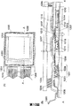
図1は、実施の形態1を示す本発明の成膜装置の断面図である。
図2は、実施の形態2を示す本発明の成膜装置の断面図である。
図3は、実施の形態3を示す本発明の成膜装置の断面図である。
図4は、実施の形態4を示す本発明の成膜装置の断面図である。
図5は、実施例1を示す本発明の成膜装置により作製される素子構造を説明する図である。
図6は、実施例2を示すマルチチャンバー方式の製造装置を示す図である。
図7は、実施例2を示す設置室におけるルツボ搬送を示す図である。
図8は、実施例2を示す設置室における蒸着源ホルダへのルツボ搬送を示す図である。
図9は、実施例3を示す図である。
図10は、実施例3を示す図である。
図11は、実施例4を示す図である。
図12は、実施例5を示す図である。
図13は、実施例6を示す図である。
図14は、実施例7を示すインライン方式の製造装置を示す図である。FIG. 1 is a cross-sectional view of a film forming apparatus of the present invention showing Embodiment Mode 1. In FIG.
FIG. 2 is a cross-sectional view of the film forming apparatus of the present invention showing the second embodiment.
FIG. 3 is a cross-sectional view of the film forming apparatus of the present invention showing the third embodiment.
FIG. 4 is a cross-sectional view of the film forming apparatus of the present invention showing Embodiment 4. In FIG.
FIG. 5 is a diagram for explaining an element structure manufactured by the film forming apparatus of the present invention showing Example 1. In FIG.
FIG. 6 is a diagram illustrating a multi-chamber manufacturing apparatus according to the second embodiment.
FIG. 7 is a diagram illustrating the crucible conveyance in the installation chamber showing the second embodiment.
FIG. 8 is a diagram illustrating the crucible conveyance to the vapor deposition source holder in the installation chamber showing the second embodiment.
FIG. 9 is a diagram illustrating the third embodiment.
FIG. 10 is a diagram illustrating the third embodiment.
FIG. 11 is a diagram illustrating a fourth embodiment.
FIG. 12 is a diagram illustrating the fifth embodiment.
FIG. 13 is a diagram illustrating the sixth embodiment.
FIG. 14 is a diagram illustrating an inline manufacturing apparatus according to the seventh embodiment.
本発明の実施形態について、以下に説明する。
(実施の形態1)
本発明における成膜装置の構成について図1を用いて説明する。図1は、本発明の成膜装置における断面図の一例である。
蒸着法による成膜を行う際、フェイスダウン方式(デポアップ方式ともいう)とすることが好ましく、基板10は、被成膜面を下向きにしてセットされている。フェイスダウン方式とは、基板の被成膜面が下を向いた状態で成膜する方式をいい、この方式によればゴミの付着などを抑えることができる。
図1に示すように、基板10に接して加熱手段、ここでは基板ホルダ12にヒータが備えられている。加熱手段によって、基板の温度は、50〜200℃、好ましくは65〜150℃とすることができる。また、基板10は、基板ホルダに内蔵された永久磁石によってメタルマスク(図示しない)で挟むことによって固定される。また、成膜室内に設置された定盤18には、それぞれ異なる温度に加熱することも可能な蒸着セル(蒸着ホルダとも呼ばれる)13が設けられている。なお、基板に対向するように蒸着源が設けられている。ここでは永久磁石を使って基板をメタルマスクで挟むことにより固定した例を示したが、ホルダで固定してもよい。
ここでは、蒸着源とは、蒸着セル13と、有機化合物を収納する容器(ルツボ、蒸着ボートなど)と、シャッター14と、有機化合物を加熱する加熱手段と、回りを囲む断熱材とで構成されている。加熱手段としては、抵抗加熱型を基本とするが、クヌーセンセルを用いてもよい。
また、成膜室には、蒸着時に材料ガスを成膜室に数sccm導入するガス導入系と、成膜室内を常圧にするガス導入系とが連結されている。材料ガスとしては、モノシラン、ジシラン、トリシラン、SiF4、GeH4、GeF4、SnH4、CH4、C2H2、C2H4、またはC6H6から選ばれた一種または複数種を用いる。なお、ガス導入口から最短距離でガス排出口に材料ガスが流れないようにすることが望ましい。
チャンバー壁11に囲まれた空間を減圧手段(ターボ分子ポンプ16やドライポンプやクライオポンプ17などの真空ポンプ)で5×10⁻³Torr(0.665Pa)以下、好ましくは1×10⁻³Torr(0.133Pa)以下とし、蒸着セルに設けられた加熱手段(電圧が印加された際に生じる抵抗(抵抗加熱))により内部の有機化合物が昇華温度まで加熱されると、気化して基板10の表面へ蒸着される。この蒸着の際に材料ガスを数sccm導入することによって膜中に材料ガスの成分を含有させる。なお、図1では、蒸発させた第1の材料15aと、蒸発させた第2の材料15bとが混ざるように一方のセルを傾けて共蒸着を行っており、さらに導入した材料ガスも混合されて膜が形成される例を示している。共蒸着とは、異なる蒸着源を加熱して同時に気化させ、成膜段階で異なる物質を混合する蒸着法を指している。また、蒸着の際、膜厚を均一にするため、基板ホルダ12は回転させる。
なお、基板10の表面とは本明細書中では、基板とその上に形成された薄膜も含むこととし、ここでは、基板上に陽極または陰極が形成されているものとする。
なお、シャッター14は、気化した有機化合物の蒸着を制御する。つまり、シャッターが開いているとき、加熱により気化した有機化合物を蒸着することができる。さらに基板10とシャッター14との間に別のシャッター(例えば、蒸着源からの昇華が安定するまでの間、蒸着源を覆っておくシャッター)を一つまたは複数設けてもよい。
なお、有機化合物は、蒸着前から加熱して気化させておき、蒸着時にシャッター14を開ければすぐに蒸着ができるようにしておくと、成膜時間を短縮できるので望ましい。
また、本発明における成膜装置においては、一つの成膜室において複数の機能領域を有する有機化合物膜を形成することが可能となっており、蒸着源もそれに応じて複数設けられている。
また、蒸着時に有機化合物が成膜室の内壁に付着することを防止するための防着板19が設けられている。この防着板19を設けることにより、基板上に蒸着されなかった有機化合物を付着させることができる。
また、成膜室には、成膜室内を真空にする複数の真空排気処理室と連結されている。真空排気処理室としては、磁気浮上型のターボ分子ポンプ16とクライオポンプ17とが備えられている。これにより成膜室の到達真空度を10−5〜10−6Torrにすることが可能である。なお、クライオポンプ17で真空排気を行った後、クライオポンプ17を停止し、ターボ分子ポンプ16で真空排気を行いつつ、材料ガスを数sccm流しながら蒸着を行うこととする。蒸着が終了したら、ターボ分子ポンプで排気しながら不活性ガスを導入して圧力をある程度上げ、残留している材料ガスを成膜室内から排出し、再び高真空排気を行う。最後に成膜室内からロード室へ真空を保ちつつ蒸着された基板を搬出する。
また、チャンバー壁11に用いる材料としては、その表面積を小さくすることで酸素や水等の不純物の吸着性を小さくすることができるので、電解研磨を施して鏡面化させたアルミニウムやステンレス(SUS)等を内部壁面に用いる。これにより、成膜室内部の真空度を10−5〜10−6Torrに維持することができる。また、気孔がきわめて少なくなるように処理されたセラミックス等の材料を内部部材に用いる。なお、これらは、中心線平均粗さが3nm以下となる表面平滑性を有するものが好ましい。
図1に示す成膜装置を用いれば、成膜時に意図的に材料ガスを導入し、材料ガスの成分を有機化合物膜中に含ませることによって高密度な膜とすることができる。材料ガスの成分を有機化合物膜中に含ませることによって劣化を引き起こす酸素や水分などの不純物が膜中に侵入、拡散することをブロッキングし、発光素子の信頼性を向上させることができる。
例えば、有機材料を蒸発させて蒸着を行っている成膜室にモノシランガスを数sccm導入すると、蒸着源から蒸発して基板に向かう有機材料と一緒に成膜室内に浮遊しているSiH4が有機膜中に取り込まれる。即ち、比較的に粒子半径の大きい有機材料分子の隙間に原子半径の小さいSiH4をそのまま、或いはSiHxで埋めることになり、有機膜中に含ませることができる。蒸着中、蒸着源は100℃程度には加熱するが、モノシランの分解温度(大気圧での分解温度)は約550℃であるので分解はしない。蒸発させる有機材料によってはSiH4、或いはSiHxと反応して化合物を形成する場合もある。また、成膜室中に僅かに残っている酸素(または水分)を捕獲してSiOxを生成するため、成膜室中および膜中において有機材料を劣化させる要因となる酸素(または水分)を減らすことができ、結果的に発光素子の信頼性を向上させることができる。また、生成されたSiOxはそのまま膜中に含ませてもよい。
膜中において有機材料分子の隙間があると、その隙間に酸素が入りやすく劣化が生じると考えられる。従って、この隙間を埋めればよいため、SiF4、GeH4、GeF4、SnH4、または炭化水素系ガス(CH4、C2H2、C2H4、C6H6等)を用いても発光素子の信頼性を向上させることができる。
なお、上記有機材料としては、α−NPD(4,4’−ビス−[N−(ナフチル)−N−フェニル−アミノ]ビフェニル)、BCP(バソキュプロイン)、MTDATA(4,4’,4”−トリス(N−3−メチルフェニル−N−フェニル−アミノ)トリフェニルアミン)、Alq3(トリス−8−キノリノラトアルミニウム錯体)などを挙げることができる。
以下に図1の成膜装置を用い、陽極と、該陽極に接する有機化合物層と、該有機化合物層に接する陰極とを有する発光素子の作製手順の一例を示す。
まず、陽極が形成された基板を搬入室(図示しない)に搬入する。陽極を形成する材料は、透明導電性材料が用いられ、インジウム・スズ化合物や酸化亜鉛などを用いることができる。次いで搬入室(図示しない)に連結された成膜前処理室(図示しない)に搬送する。この成膜前処理室では、陽極表面のクリーニングや酸化処理や加熱処理などを行えばよい。陽極表面のクリーニングとしては、真空中での紫外線照射を行い、陽極表面をクリーニングする。また、酸化処理としては、100〜120℃で加熱しつつ、酸素を含む雰囲気中で紫外線を照射すればよく、陽極がITOのような酸化物である場合に有効である。また、加熱処理としては、真空中で基板が耐えうる50℃以上の加熱温度、好ましくは65〜150℃の加熱を行えばよく、基板に付着した酸素や水分などの不純物や、基板上に形成した膜中の酸素や水分などの不純物を除去する。特に、EL材料は、酸素や水などの不純物により劣化を受けやすいため、蒸着前に真空中で加熱することは有効である。
次いで、上記前処理が終わった基板を大気にふれさせることなく、成膜室に搬入する。成膜室には、基板10の被成膜面を下向きにしてセットする。なお、基板を搬入する前に成膜室内は真空排気しておくことが好ましい。
成膜室に連結して設けられる真空排気手段は、大気圧から1Pa程度をオイルフリーのドライポンプで真空排気し、それ以上の圧力は磁気浮上型のターボ分子ポンプ16により真空排気する。さらに成膜室には水分を除去するためにクライオポンプ17を併設している。こうして、1×10⁻⁶Torrまでの真空度を実現する。
成膜室内を真空排気する際、同時に成膜室内壁やメタルマスクや防着シールドなどに付着した吸着水や吸着酸素を除去することも可能である。さらに、基板を搬入する前に成膜室を加熱しておくことが好ましい。前処理で加熱した基板を徐冷させて、成膜室に搬入した後、再び加熱することは長時間かかり、スループットの低下を招くことになる。望ましくは、前処理で行った加熱処理で加熱した基板を冷却することなく、そのまま加熱された成膜室に搬入及びセットする。なお、図1に示す装置は、基板ホルダ12に基板を加熱する加熱手段が設けられているため、前処理である真空中での加熱処理を成膜室で行うことも可能である。
ここでは、蒸着を行う前に成膜室で真空中での加熱処理(アニール)を行う。このアニール(脱気)によって基板に付着した酸素や水分などの不純物や、基板上に形成した膜中の酸素や水分などの不純物を除去する。こうして除去された不純物を成膜室から除去するため、真空排気を行うことが好ましく、さらに真空度を高めてもよい。
次いで、材料ガスを数sccm導入しながら、真空度が5×10⁻³Torr(0.665Pa)以下、好ましくは10−4〜10−6Torrまで真空排気された成膜室で蒸着を行う。蒸着の際、予め、抵抗加熱により第一の有機化合物は気化されており、蒸着時にシャッター14が開くことにより基板10の方向へ飛散する。気化された有機化合物は、上方に飛散し、材料ガスと混ざり、メタルマスクに設けられた開口部(図示せず)を通って基板10に蒸着される。なお、蒸着の際、基板を加熱する手段により基板の温度は、50〜200℃、好ましくは65〜150℃とする。
図1に示す装置では、基板を加熱する加熱手段が設けられ、成膜中において真空中での加熱処理が行われる。蒸着時の蒸発材料には、酸素や水分などの不純物が混入している恐れがあるため、蒸着中に真空中で加熱処理を行って膜中に含まれるガスを放出させることは有効である。このように、真空中で基板を加熱しながら蒸着を行い、所望の膜厚まで成膜を行うことによって、高密度な有機化合物層を形成することができる。なお、ここでいう有機化合物とは、陽極から正孔を受け取る正孔注入性、電子移動度よりも正孔移動度の方が大きい正孔輸送性、正孔移動度よりも電子移動度の方が大きい電子輸送性、陰極から電子を受け取る電子注入性、正孔または電子の移動を阻止しうるブロッキング性、発光を呈する発光性、といった性質を有する有機化合物である。
こうして、有機化合物の蒸着が終了し、有機化合物からなる膜が、陽極上に形成される。
さらに、得られた有機化合物層中の水分や酸素の不純物を低減するために、1×10⁻⁴Torr以下の圧力で加熱処理を行い、蒸着時に混入した水分などを放出させる加熱処理を行っても良い。蒸着時の蒸発材料には、酸素や水分などの不純物が混入している恐れがあるため、蒸着後に真空中で加熱処理を行って膜中に含まれるガスを放出させることは有効である。蒸着後のアニールを行う場合、大気にふれることなく、成膜室とは別の処理室に基板を搬送して、真空中でアニールを行うことが好ましい。
図1に示す装置は、基板を加熱する加熱手段が設けられているため、成膜後に真空中での加熱処理を成膜室で行うことも可能である。蒸着の際の真空度よりもさらに高真空として、蒸着後、100〜200℃のアニールを行うことが好ましい。この成膜後のアニール(脱気)によって基板上に形成した有機化合物層中の酸素や水分などの不純物をさらに除去し、高密度な有機化合物層を形成する。
有機化合物層中には、材料ガスまたは材料ガスの主成分、例えば蒸着の際にモノシランガスを導入した場合、珪素がSIMS測定で0.01atoms%〜5atoms%、好ましくは0.1atoms%〜2atoms%程度含まれるようにする。図1に示す成膜装置を用いて成膜された有機化合物を含む膜は、材料ガスまたは材料ガスの主成分を含み、酸素や水分を取り込みにくい膜となるため、この有機化合物を含む膜を用いた発光素子は信頼性が向上する。
ここまで示した工程は、有機化合物の単層を形成する場合である。
以降、上記単層の形成工程を繰り返すことによって、所望の有機化合物層を積層し、最後に陰極を積層形成する。なお、異なる蒸着材料(有機化合物や陰極の材料)を積層する場合、別々の成膜室で行ってもよいし、全て同一の成膜室で積層してもよい。陰極の材料は、仕事関数の小さいマグネシウム(Mg)、リチウム(Li)若しくはカルシウム(Ca)を含む材料を用いる。好ましくはMgAg(MgとAgをMg:Ag=10:1で混合した材料)でなる電極を用いれば良い。他にも、イッテルビウム(Yb)、MgAgAl電極、LiAl電極、また、LiFAl電極が挙げられる。こうして、陽極と、該陽極に接する有機化合物層と、該有機化合物層に接する陰極とを有する発光素子を作製できる。また、成膜前のアニールを成膜室で行うことが可能であり、その場合、スループットが向上する。また、成膜後のアニールを成膜室で行うことが可能であり、その場合、スループットが向上する。
(実施の形態2)
ここでは、実施の形態1と異なる成膜装置を図2に示す。
図2には、膜が均一に成膜されるように、蒸着源が移動(または回転)する成膜装置の例を示す。
図2中、20は基板、21はチャンバー壁、22は基板ホルダ、23はセル、25aは蒸発させた第1の材料、25bは蒸発させた第2の材料、26はターボ分子ポンプ、27はクライオポンプ、28はセルを移動させる移動機構である。基板を回転させる必要がないため、大面積基板に対応可能な蒸着装置を提供することができる。また、蒸着セル23が基板に対してX軸方向及びY軸方向に移動することにより、蒸着膜を均一に成膜することが可能となる。
本発明の蒸着装置においては、蒸着の際、基板20と蒸着セル23との間隔距離dを代表的には30cm以下、好ましくは20cm以下、さらに好ましくは5cm〜15cmに狭め、蒸着材料の利用効率及びスループットを格段に向上させている。
また、蒸着セル23に備えられる有機化合物は必ずしも一つまたは一種である必要はなく、複数であってもよい。例えば、蒸着源ホルダに発光性の有機化合物として備えられている一種類の材料の他に、ドーパントとなりうる別の有機化合物(ドーパント材料)を一緒に備えておいても良い。蒸着させる有機化合物層として、ホスト材料と、ホスト材料よりも励起エネルギーが低い発光材料(ドーパント材料)とで構成し、ドーパントの励起エネルギーが、正孔輸送性領域の励起エネルギーおよび電子輸送層の励起エネルギーよりも低くなるように設計することが好ましい。このことにより、ドーパントの分子励起子の拡散を防ぎ、効果的にドーパントを発光させることができる。また、ドーパントがキャリアトラップ型の材料であれば、キャリアの再結合効率も高めることができる。また、三重項励起エネルギーを発光に変換できる材料をドーパントとして混合領域に添加した場合も本発明に含めることとする。また、混合領域の形成においては、混合領域に濃度勾配をもたせてもよい。
さらに、一つの蒸着源ホルダに備えられる有機化合物を複数とする場合、互いの有機化合物が混ざりあうように蒸発する方向を被蒸着物の位置で交差するように斜めにすることが望ましい。また、共蒸着を行うため、蒸着セルに、4種の蒸着材料(例えば、蒸着材料aとしてホスト材料2種類、蒸着材料bとしてドーパント材料2種類)を備えてもよい。
また、蒸着させるEL材料や金属材料に対して、酸素や水等の不純物が混入する恐れのある主な過程を挙げた場合、蒸着前にEL材料を成膜室にセットする過程、蒸着過程などが考えられる。
そこで、成膜室に連結した前処理室にグローブを備え、蒸着源ごと成膜室から前処理室に移動させ、前処理室で蒸着源に蒸着材料をセットすることが好ましい。即ち、蒸着源が前処理室まで移動する製造装置とする。こうすることによって、成膜室の洗浄度を保ったまま、蒸着源をセットすることができる。
図2に示す成膜装置においても、成膜時に意図的に材料ガスを導入し、材料ガスの成分を有機化合物膜中に含ませることによって高密度な膜とすることができる。材料ガスの成分を有機化合物膜中に含ませることによって劣化を引き起こす酸素や水分などの不純物が膜中に侵入、拡散することをブロッキングし、発光素子の信頼性を向上させることができる。
また、本実施の形態は、実施の形態1と自由に組み合わせることが可能である。
(実施の形態3)
ここでは、実施の形態1と異なる成膜装置を図3に示す。なお、図1と同じ箇所には同じ符号を用いる。
図3に示す成膜装置は、予めプラズマ発生手段によってラジカル化させた材料ガスを成膜室に導入しながら蒸着を行う例である。
図3に示すように、マイクロ波ソース30aが導波管30bに接続されている。この導波管30bは、放電管中の材料ガスに照射を行ってグロー放電によるプラズマ30cを形成する。ここで用いるマイクロ波ソースからは、約2.45GHzのμ波が放射される。
例えば、材料ガスとしてモノシランガスを用いた場合、SiHx、SiHxOy、SiOyなどの酸化シリコン前駆体が生成され、成膜室内に導入される。これらのラジカルは、酸素や水分と反応しやすく、成膜室内の酸素濃度や水分量を低減することができ、結果的に信頼性の高い有機化合物膜を得ることができる。
また、これらのラジカルは、より温度の高い場所に移動、または堆積しやすいため、基板ホルダ12に設けられているヒータ31で基板を加熱しながら蒸着を行うことが好ましい。また、蒸着セル13に移動、または堆積するのを防ぐため、蒸着セル13は断熱材で覆うことが好ましい。
また、本実施の形態は、実施の形態1または実施の形態2と自由に組み合わせることが可能である。
(実施の形態4)
ここでは、実施の形態1と異なる成膜装置を図4に示す。
図4に示す成膜装置は、イオンプレーティング法を用い、成膜室内で材料ガスをイオン化させ、蒸発させた有機材料65に付着させながら蒸着を行う例である。
図4中、60は基板、61はチャンバー壁、62は基板ホルダ、63はセル、65は蒸発させた有機材料、66はターボ分子ポンプ、67はクライオポンプ、68は定盤、69防着板である。
図4に示す成膜装置には、材料51を収納したルツボ52に電子ビームを照射する電子銃50、プラズマ53を発生させるプラズマ発生手段64が設けられている。
電子銃50により電子ビームをルツボ52に照射してルツボ内の材料51を溶解、蒸発させて材料51の蒸発流を形成し、プラズマ発生手段64によりイオン化させ、イオン化した蒸発流と、蒸着セル63から蒸発させた有機材料65とを混合させ、これらを基板に衝突させて成膜する。
図4に示す成膜装置においては、有機材料の蒸着の途中で蒸発した材料51を化学付着させ、材料51の成分を有機化合物膜中に含ませることによって高密度な膜とすることができる。材料51の成分を有機化合物膜中に含ませることによって劣化を引き起こす酸素や水分などの不純物が膜中に侵入、拡散することをブロッキングし、発光素子の信頼性を向上させることができる。
また、本実施の形態は、実施の形態1乃至3のいずれか一と自由に組み合わせることができる。
以上の構成でなる本発明について、以下に示す実施例でもってさらに詳細な説明を行うこととする。Embodiments of the present invention will be described below.
(Embodiment 1)
The structure of the film forming apparatus in the present invention will be described with reference to FIG. FIG. 1 is an example of a cross-sectional view of a film forming apparatus of the present invention.
When performing film formation by vapor deposition, it is preferable to employ a face-down method (also referred to as a deposition method), and the
As shown in FIG. 1, a heater is provided in the heating means, here, the
Here, the vapor deposition source is composed of a
In addition, a gas introduction system for introducing a material gas into the film formation chamber at several sccm during vapor deposition and a gas introduction system for bringing the film formation chamber to normal pressure are connected to the film formation chamber. As the material gas, one or more kinds selected from monosilane, disilane, trisilane, SiF 4 , GeH 4 , GeF 4 , SnH 4 , CH 4 , C 2 H 2 , C 2 H 4 , or C 6 H 6 are used. Use. It is desirable to prevent the material gas from flowing to the gas outlet at the shortest distance from the gas inlet.
The space surrounded by the
In this specification, the surface of the
The
Note that it is desirable that the organic compound be vaporized by heating before vapor deposition, and that the vapor deposition can be performed as soon as the
In the film forming apparatus of the present invention, an organic compound film having a plurality of functional regions can be formed in one film forming chamber, and a plurality of vapor deposition sources are provided accordingly.
In addition, an
The film formation chamber is connected to a plurality of vacuum exhaust processing chambers that evacuate the film formation chamber. As the evacuation processing chamber, a magnetic levitation turbo
Further, as the material used for the
If the film forming apparatus shown in FIG. 1 is used, a material gas is intentionally introduced at the time of film formation, and a component of the material gas is included in the organic compound film, whereby a high-density film can be obtained. By including a component of the material gas in the organic compound film, impurities such as oxygen and moisture that cause deterioration can be blocked from entering and diffusing into the film, and the reliability of the light emitting element can be improved.
For example, when monosilane gas is introduced into the film formation chamber where the organic material is evaporated and vapor deposition is performed, SiH 4 floating in the film formation chamber together with the organic material evaporated from the vapor deposition source and directed toward the substrate is organic. It is taken into the membrane. That is, SiH 4 having a small atomic radius is filled in a gap between organic material molecules having a relatively large particle radius as it is or with SiH x and can be included in the organic film. During the vapor deposition, the vapor deposition source is heated to about 100 ° C., but the decomposition temperature (decomposition temperature at atmospheric pressure) of monosilane is about 550 ° C., so it is not decomposed. Depending on the organic material to be evaporated, it may react with SiH 4 or SiH x to form a compound. Further, since oxygen (or moisture) remaining slightly in the deposition chamber is captured to generate SiO x , oxygen (or moisture) that causes deterioration of the organic material in the deposition chamber and in the film is removed. As a result, the reliability of the light-emitting element can be improved. Further, the generated SiOx may be included in the film as it is.
If there is a gap between organic material molecules in the film, it is considered that oxygen easily enters the gap and deteriorates. Therefore, since it is sufficient to fill this gap, SiF 4 , GeH 4 , GeF 4 , SnH 4 , or hydrocarbon-based gas (CH 4 , C 2 H 2 , C 2 H 4 , C 6 H 6, etc.) is used. In addition, the reliability of the light emitting element can be improved.
Examples of the organic material include α-NPD (4,4′-bis- [N- (naphthyl) -N-phenyl-amino] biphenyl), BCP (bathocuproine), MTDATA (4,4 ′, 4 ″- And tris (N-3-methylphenyl-N-phenyl-amino) triphenylamine) and Alq 3 (tris-8-quinolinolato aluminum complex).
An example of a procedure for manufacturing a light-emitting element using the film formation apparatus in FIG. 1 and including an anode, an organic compound layer in contact with the anode, and a cathode in contact with the organic compound layer is described below.
First, the substrate on which the anode is formed is carried into a carry-in chamber (not shown). As a material for forming the anode, a transparent conductive material is used, and an indium / tin compound, zinc oxide, or the like can be used. Next, the film is transferred to a pre-deposition treatment chamber (not shown) connected to a carry-in chamber (not shown). In the pre-deposition treatment chamber, the anode surface may be cleaned, oxidized, heated, or the like. As the cleaning of the anode surface, ultraviolet irradiation is performed in vacuum to clean the anode surface. In addition, the oxidation treatment may be performed by irradiating ultraviolet rays in an atmosphere containing oxygen while heating at 100 to 120 ° C., and is effective when the anode is an oxide such as ITO. The heat treatment may be performed at a heating temperature of 50 ° C. or higher, preferably 65 to 150 ° C. that the substrate can withstand in vacuum, and is formed on the substrate by impurities such as oxygen and moisture attached to the substrate. Impurities such as oxygen and moisture in the deposited film are removed. In particular, since the EL material is easily deteriorated by impurities such as oxygen and water, it is effective to heat in vacuum before vapor deposition.
Next, the substrate after the pretreatment is carried into the film formation chamber without being exposed to the atmosphere. In the film forming chamber, the film forming surface of the
The vacuum evacuation means provided in connection with the film forming chamber evacuates from atmospheric pressure to about 1 Pa with an oil-free dry pump, and the pressure higher than that is evacuated with a magnetic levitation turbo
When the film forming chamber is evacuated, it is possible to remove adsorbed water and oxygen adhering to the film forming chamber wall, metal mask, deposition shield, and the like at the same time. Furthermore, it is preferable to heat the film formation chamber before carrying in the substrate. It takes a long time to slowly cool the substrate heated in the pretreatment, carry it into the film formation chamber, and then reduce the throughput. Desirably, the substrate heated by the heat treatment performed in the pretreatment is carried and set in the heated film formation chamber without being cooled. In the apparatus shown in FIG. 1, since the
Here, heat treatment (annealing) is performed in a vacuum in a film formation chamber before vapor deposition. By this annealing (deaeration), impurities such as oxygen and moisture attached to the substrate and impurities such as oxygen and moisture in the film formed on the substrate are removed. In order to remove the impurities thus removed from the film formation chamber, it is preferable to perform evacuation, and the degree of vacuum may be further increased.
Next, while introducing a material gas of several sccm, the degree of vacuum is 5 × 10 −3 Torr (0.665 Pa) or less, preferably 10 −4 to 10 −6 Torr. At the time of vapor deposition, the first organic compound is vaporized in advance by resistance heating, and is scattered toward the
In the apparatus shown in FIG. 1, heating means for heating the substrate is provided, and heat treatment is performed in vacuum during film formation. Since there is a possibility that impurities such as oxygen and moisture may be mixed in the evaporation material at the time of vapor deposition, it is effective to release the gas contained in the film by performing a heat treatment in vacuum during the vapor deposition. Thus, a high-density organic compound layer can be formed by performing vapor deposition while heating the substrate in vacuum and forming a film to a desired film thickness. In addition, the organic compound here refers to a hole injection property that receives holes from the anode, a hole mobility that is larger than the electron mobility, and an electron mobility that is higher than the hole mobility. Is an organic compound having properties such as a large electron transport property, an electron injection property of receiving electrons from the cathode, a blocking property capable of preventing the movement of holes or electrons, and a light emission property of emitting light.
Thus, the vapor deposition of the organic compound is completed, and a film made of the organic compound is formed on the anode.
Furthermore, in order to reduce moisture and oxygen impurities in the obtained organic compound layer, heat treatment is performed at a pressure of 1 × 10 −4 Torr or less, and heat treatment is performed to release moisture mixed in during the deposition. Also good. Since there is a possibility that impurities such as oxygen and moisture may be mixed in the evaporation material at the time of vapor deposition, it is effective to release the gas contained in the film by performing a heat treatment in vacuum after the vapor deposition. In the case of performing annealing after vapor deposition, it is preferable to carry out the annealing in a vacuum by transporting the substrate to a processing chamber different from the deposition chamber without being exposed to the atmosphere.
Since the apparatus illustrated in FIG. 1 is provided with a heating unit that heats the substrate, heat treatment in vacuum can be performed in the deposition chamber after deposition. It is preferable to perform annealing at 100 to 200 ° C. after the deposition, with a higher vacuum than the degree of vacuum at the time of deposition. Impurities such as oxygen and moisture in the organic compound layer formed on the substrate are further removed by annealing (deaeration) after the film formation to form a high-density organic compound layer.
In the organic compound layer, when a material gas or a main component of the material gas, for example, a monosilane gas is introduced at the time of vapor deposition, silicon is about 0.01 atoms% to 5 atoms%, preferably about 0.1 atoms% to 2 atoms% in SIMS measurement. To be included. A film containing an organic compound formed using the film formation apparatus shown in FIG. 1 contains a material gas or a main component of a material gas and is difficult to take in oxygen and moisture. The reliability of the used light emitting element is improved.
The steps described so far are cases where a single layer of an organic compound is formed.
Thereafter, by repeating the single layer forming step, a desired organic compound layer is laminated, and finally a cathode is laminated. Note that when different vapor deposition materials (organic compounds and cathode materials) are stacked, they may be stacked in separate film forming chambers or may be stacked in the same film forming chamber. As a material for the cathode, a material containing magnesium (Mg), lithium (Li), or calcium (Ca) having a small work function is used. An electrode made of MgAg (a material in which Mg and Ag are mixed at Mg: Ag = 10: 1) is preferably used. Other examples include ytterbium (Yb), MgAgAl electrode, LiAl electrode, and LiFAl electrode. Thus, a light-emitting element having an anode, an organic compound layer in contact with the anode, and a cathode in contact with the organic compound layer can be manufactured. In addition, annealing before film formation can be performed in the film formation chamber, in which case throughput is improved. Further, annealing after film formation can be performed in the film formation chamber, and in this case, throughput is improved.
(Embodiment 2)
Here, a film formation apparatus different from that in Embodiment Mode 1 is shown in FIG.
FIG. 2 shows an example of a film forming apparatus in which the vapor deposition source moves (or rotates) so that the film is formed uniformly.
In FIG. 2, 20 is a substrate, 21 is a chamber wall, 22 is a substrate holder, 23 is a cell, 25a is an evaporated first material, 25b is an evaporated second material, 26 is a turbo molecular pump, and 27 is A
In the vapor deposition apparatus of the present invention, during vapor deposition, the distance d between the
Moreover, the organic compound with which the
Further, when a plurality of organic compounds are provided in one vapor deposition source holder, it is desirable that the evaporation direction is oblique so as to intersect at the position of the vapor deposition object so that the organic compounds are mixed with each other. In order to perform co-evaporation, the deposition cell may be provided with four types of deposition materials (for example, two types of host materials as the deposition material a and two types of dopant materials as the deposition material b).
In addition, when the main process in which impurities such as oxygen and water may be mixed into the EL material or metal material to be deposited is given, the process of setting the EL material in the film formation chamber before the deposition, the deposition process, etc. Can be considered.
Therefore, it is preferable that the pretreatment chamber connected to the film formation chamber is provided with a globe, the vapor deposition source is moved from the film formation chamber to the pretreatment chamber, and the vapor deposition material is set in the vapor deposition source in the pretreatment chamber. That is, the manufacturing apparatus moves the vapor deposition source to the pretreatment chamber. By doing so, the vapor deposition source can be set while maintaining the cleanliness of the film forming chamber.
Also in the film forming apparatus shown in FIG. 2, a high-density film can be formed by intentionally introducing a material gas at the time of film formation and including the component of the material gas in the organic compound film. By including a component of the material gas in the organic compound film, impurities such as oxygen and moisture that cause deterioration can be blocked from entering and diffusing into the film, and the reliability of the light emitting element can be improved.
Further, this embodiment mode can be freely combined with Embodiment Mode 1.
(Embodiment 3)
Here, a film formation apparatus different from that in Embodiment Mode 1 is shown in FIG. In addition, the same code | symbol is used for the same location as FIG.
The film forming apparatus shown in FIG. 3 is an example in which vapor deposition is performed while introducing a material gas radicalized in advance by plasma generating means into a film forming chamber.
As shown in FIG. 3, a
For example, when monosilane gas is used as the material gas, silicon oxide precursors such as SiHx, SiHxOy, and SiOy are generated and introduced into the deposition chamber. These radicals easily react with oxygen and moisture, can reduce the oxygen concentration and the amount of moisture in the deposition chamber, and as a result, a highly reliable organic compound film can be obtained.
In addition, since these radicals are easily moved or deposited at a higher temperature, it is preferable to perform vapor deposition while heating the substrate with the
Further, this embodiment mode can be freely combined with Embodiment Mode 1 or Embodiment Mode 2.
(Embodiment 4)
Here, a film formation apparatus different from that in Embodiment Mode 1 is shown in FIG.
The film formation apparatus shown in FIG. 4 is an example in which vapor deposition is performed while ionizing a material gas in a film formation chamber and attaching it to the evaporated
In FIG. 4, 60 is a substrate, 61 is a chamber wall, 62 is a substrate holder, 63 is a cell, 65 is an evaporated organic material, 66 is a turbo molecular pump, 67 is a cryopump, 68 is a surface plate, and 69 deposition plate. It is.
The film forming apparatus shown in FIG. 4 is provided with an
An electron beam is applied to the
In the film forming apparatus shown in FIG. 4, the
Further, this embodiment mode can be freely combined with any one of Embodiment Modes 1 to 3.
The present invention having the above-described configuration will be described in more detail with the following examples.
本実施例では、有機化合物膜中に存在するエネルギー障壁を緩和してキャリアの移動性を高めると同時に、なおかつ積層構造の機能分離と同様に各種複数の材料の機能を有する発光素子を作製する例を示す。
積層構造におけるエネルギー障壁の緩和に関しては、キャリア注入層の挿入という技術に顕著に見られる。つまり、エネルギー障壁の大きい積層構造の界面において、そのエネルギー障壁を緩和する材料を挿入することにより、エネルギー障壁を階段状に設計することができる。これにより電極からのキャリア注入性を高め、確かに駆動電圧をある程度までは下げることができる。しかしながら問題点は、層の数を増やすことによって、有機界面の数は逆に増加することである。このことが、単層構造の方が駆動電圧・パワー効率のトップデータを保持している原因であると考えられる。逆に言えば、この点を克服することにより、積層構造のメリット(様々な材料を組み合わせることができ、複雑な分子設計が必要ない)を活かしつつ、なおかつ単層構造の駆動電圧・パワー効率に追いつくことができる。
そこで本実施例において、発光素子の陽極と陰極の間に複数の機能領域からなる有機化合物膜が形成される場合、従来の明確な界面が存在する積層構造ではなく、第一の機能領域と第二の機能領域との間に、第一の機能領域を構成する材料および第二の機能領域を構成する材料の両方からなる混合領域を有する構造を形成する。
このような構造を適用することで、機能領域間に存在するエネルギー障壁は従来の構造に比較して低減され、キャリアの注入性が向上すると考えられる。すなわち機能領域間におけるエネルギー障壁は、混合領域を形成することにより緩和される。したがって、駆動電圧の低減、および輝度低下の防止が可能となる。
以上のことから、本実施例では第一の有機化合物が機能を発現できる領域(第一の機能領域)と、前記第一の機能領域を構成する物質とは異なる第二の有機化合物が機能を発現できる領域(第二の機能領域)と、を少なくとも含む発光素子、及びこれを有する発光装置の作製において、図1に示す成膜装置を用い、前記第一の機能領域と前記第二の機能領域との間に、前記第一の機能領域を構成する有機化合物と前記第二の機能領域を構成する有機化合物、とからなる混合領域を作製する。
図1に示す成膜装置において、一つの成膜室において複数の機能領域を有する有機化合物膜が形成されるようになっており、蒸着源もそれに応じて複数設けられている。なお、陽極が形成されている基板を搬入しセットする。
はじめに、第一の材料室に備えられている、第一の有機化合物が蒸着される。なお、第一の有機化合物は予め抵抗加熱により気化されており、蒸着時に第1のシャッターが開くことにより基板の方向へ飛散する。蒸着の際には材料ガス、ここではモノシランガスを導入し、膜中に含有させる。これにより、図5(A)に示す第一の機能領域210を形成することができる。
そして、第一の有機化合物17aを蒸着したまま、第2のシャッターを開け、第二の材料室に備えられている、第二の有機化合物を蒸着する。なお、第二の有機化合物も予め抵抗加熱により気化されており、蒸着時に第2のシャッターが開くことにより基板の方向へ飛散する。蒸着の際には材料ガス、ここではモノシランガスを導入し、膜中に含有させる。ここで、第一の有機化合物と第二の有機化合物とからなる第一の混合領域211を形成することができる。
そして、しばらくしてから第1のシャッターのみを閉じ、第二の有機化合物を蒸着する。蒸着の際には材料ガス、ここではモノシランガスを導入し、膜中に含有させる。これにより、第二の機能領域212を形成することができる。
なお、本実施例では、二種類の有機化合物を同時に蒸着することにより、混合領域を形成する方法を示したが、第一の有機化合物を蒸着した後、その蒸着雰囲気下で第二の有機化合物を蒸着することにより、第一の機能領域と第二の機能領域との間に混合領域を形成することもできる。
次に、第二の有機化合物を蒸着したまま、第3のシャッターを開け、第三の材料室に備えられている、第三の有機化合物を蒸着する。なお、第三の有機化合物も予め抵抗加熱により気化されており、蒸着時に第3のシャッターが開くことにより基板の方向へ飛散する。蒸着の際には材料ガス、ここではモノシランガスを導入し、膜中に含有させる。ここで、第二の有機化合物と第三の有機化合物とからなる第二の混合領域213を形成することができる。
そして、しばらくしてから第2のシャッターのみを閉じ、第三の有機化合物を蒸着する。蒸着の際には材料ガス、ここではモノシランガスを導入し、膜中に含有させる。そして第3のシャッターを閉じて第三の有機化合物の蒸着を完了させる。これにより、第三の機能領域214を形成することができる。
最後に、陰極を形成することにより本発明の成膜装置により形成される発光素子が完成する。
さらに、その他の有機化合物膜としては、図5(B)に示すように、第一の有機化合物を用いて第一の機能領域220を形成した後、第一の有機化合物と第二の有機化合物とからなる第一の混合領域221を形成し、さらに、第二の有機化合物を用いて第二の機能領域222を形成する。そして、第二の機能領域222を形成する途中で、一時的に第3のシャッターを開いて第三の有機化合物17cの蒸着を同時に行うことにより、第二の混合領域223を形成する。
しばらくして、第3のシャッターを閉じることにより、再び第二の機能領域222を形成する。そして、陰極を形成することにより発光素子が形成される。
以上のような有機化合物膜を形成することができる図2の成膜装置は、同一の成膜室において複数の機能領域を有する有機化合物膜を形成することができるので、機能領域界面に混合領域を形成することができる。以上により、明瞭な積層構造を示すことなく(すなわち、明確な有機界面がなく)、かつ、複数の機能を備えた発光素子を作製することができる。
また、図1の成膜装置は、成膜時に意図的に材料ガス(モノシランガス)を導入し、材料ガスの成分を有機化合物膜中に含ませることが可能であり、有機化合物膜中に原子半径の小さい材料(代表的にはシリコン)を含ませることによって、混合領域における分子間をよりフィットさせることができる。したがって、さらに駆動電圧の低減、および輝度低下の防止が可能となる。また、材料ガスによって成膜室内の酸素や水分などの不純物をさらに除去することもでき、高密度な有機化合物層を形成することができる。
また、本実施例は、実施の形態1、実施の形態2、実施の形態3、または実施の形態4と自由に組み合わせることが可能である。In this example, an energy barrier existing in an organic compound film is relaxed to improve carrier mobility, and at the same time, a light-emitting element having functions of a plurality of materials as in the functional separation of a stacked structure is manufactured. Indicates.
Regarding the relaxation of the energy barrier in the laminated structure, the technique of inserting a carrier injection layer is noticeable. That is, the energy barrier can be designed in a step shape by inserting a material that relaxes the energy barrier at the interface of the stacked structure having a large energy barrier. As a result, the carrier injection property from the electrode can be improved and the drive voltage can be lowered to some extent. However, the problem is that by increasing the number of layers, the number of organic interfaces increases conversely. This is considered to be the reason why the single layer structure holds the top data of the driving voltage and power efficiency. In other words, by overcoming this point, while taking advantage of the advantages of a laminated structure (a variety of materials can be combined and no complicated molecular design is required), the driving voltage and power efficiency of a single-layer structure can be achieved. I can catch up.
Therefore, in this example, when an organic compound film composed of a plurality of functional regions is formed between the anode and the cathode of the light emitting element, the first functional region and the first functional region are not the conventional laminated structure in which a clear interface exists. A structure having a mixed region made of both the material constituting the first functional region and the material constituting the second functional region is formed between the two functional regions.
By applying such a structure, it is considered that the energy barrier existing between the functional regions is reduced as compared with the conventional structure, and the carrier injection property is improved. That is, the energy barrier between the functional regions is relaxed by forming a mixed region. Therefore, it is possible to reduce the drive voltage and prevent the luminance from being lowered.
From the above, in this example, the region in which the first organic compound can function (the first functional region) and the second organic compound different from the substance constituting the first functional region function. In the manufacture of a light emitting element including at least a region that can be expressed (second functional region) and a light emitting device having the light emitting element, the first functional region and the second function are formed using the film formation apparatus illustrated in FIG. A mixed region composed of the organic compound constituting the first functional region and the organic compound constituting the second functional region is prepared between the regions.
In the film forming apparatus shown in FIG. 1, an organic compound film having a plurality of functional regions is formed in one film forming chamber, and a plurality of vapor deposition sources are provided accordingly. A substrate on which the anode is formed is carried in and set.
First, the first organic compound provided in the first material chamber is deposited. Note that the first organic compound is vaporized by resistance heating in advance, and is scattered in the direction of the substrate when the first shutter is opened during vapor deposition. In vapor deposition, a material gas, here monosilane gas, is introduced and contained in the film. Thereby, the first
Then, with the first organic compound 17a deposited, the second shutter is opened, and the second organic compound provided in the second material chamber is deposited. Note that the second organic compound is also vaporized by resistance heating in advance, and is scattered in the direction of the substrate when the second shutter is opened at the time of vapor deposition. In vapor deposition, a material gas, here monosilane gas, is introduced and contained in the film. Here, the first
Then, after a while, only the first shutter is closed and the second organic compound is deposited. In vapor deposition, a material gas, here monosilane gas, is introduced and contained in the film. Thereby, the second
In this example, a method of forming a mixed region by simultaneously depositing two kinds of organic compounds was shown. However, after depositing the first organic compound, the second organic compound was deposited in the deposition atmosphere. By vapor-depositing, a mixed region can be formed between the first functional region and the second functional region.
Next, with the second organic compound deposited, the third shutter is opened, and the third organic compound provided in the third material chamber is deposited. Note that the third organic compound is also vaporized in advance by resistance heating, and is scattered in the direction of the substrate when the third shutter is opened during vapor deposition. In vapor deposition, a material gas, here monosilane gas, is introduced and contained in the film. Here, the second mixed region 213 composed of the second organic compound and the third organic compound can be formed.
Then, after a while, only the second shutter is closed and a third organic compound is deposited. In vapor deposition, a material gas, here monosilane gas, is introduced and contained in the film. Then, the third shutter is closed to complete the deposition of the third organic compound. Thereby, the third
Finally, a light emitting element formed by the film forming apparatus of the present invention is completed by forming a cathode.
Furthermore, as another organic compound film, as shown in FIG. 5B, after the first
After a while, the second
The film forming apparatus of FIG. 2 capable of forming the organic compound film as described above can form an organic compound film having a plurality of functional regions in the same film forming chamber. Can be formed. As described above, a light-emitting element having a plurality of functions can be manufactured without showing a clear stacked structure (that is, without a clear organic interface).
In addition, the film forming apparatus of FIG. 1 can intentionally introduce a material gas (monosilane gas) at the time of film formation so that the component of the material gas is included in the organic compound film, and the atomic radius is included in the organic compound film. By including a small material (typically silicon), the molecules in the mixed region can be more fitted. Therefore, it is possible to further reduce the driving voltage and prevent the luminance from being lowered. Further, impurities such as oxygen and moisture in the film formation chamber can be further removed by the material gas, so that a high-density organic compound layer can be formed.
Further, this embodiment can be freely combined with Embodiment Mode 1, Embodiment Mode 2, Embodiment Mode 3, or Embodiment Mode 4.
本実施例では、第1の電極から封止までの作製を全自動化したマルチチャンバー方式の製造装置の例を図6に示す。
図6は、ゲート500a〜500yと、搬送室502、504a、508、514、518と、受渡室505、507、511と、仕込室501と、第1成膜室506Hと、第2成膜室506Bと、第3成膜室506Gと、第4成膜室506R、第5成膜室506Eと、その他の成膜室509、510、512、513、531、532と、蒸着源を設置する設置室526R、526G、526B、526E、526Hと、前処理室503a、503bと、封止室516と、マスクストック室524と、封止基板ストック室530と、カセット室520a、520bと、トレイ装着ステージ521と、取出室519と、を有するマルチチャンバーの製造装置である。なお、搬送室504aには基板504cを搬送するための搬送機構504bが設けており、他の搬送室も同様にそれぞれ搬送機構が設けてある。
以下、予め陽極(第1の電極)と、該陽極の端部を覆う絶縁物(隔壁)とが設けられた基板を図6に示す製造装置に搬入し、発光装置を作製する手順を示す。なお、アクティブマトリクス型の発光装置を作製する場合、予め基板上には、陽極に接続している薄膜トランジスタ(電流制御用TFT)およびその他の薄膜トランジスタ(スイッチング用TFTなど)が複数設けられ、薄膜トランジスタからなる駆動回路も設けられている。また、単純マトリクス型の発光装置を作製する場合にも図6に示す製造装置で作製することが可能である。
まず、カセット室520aまたはカセット室520bに上記基板をセットする。基板が大型基板(例えば300mm×360mm)である場合はカセット室520bにセットし、通常基板(例えば、127mm×127mm)である場合には、カセット室520aにセットした後、トレイ装着ステージ521に搬送し、トレイ(例えば300mm×360mm)に複数の基板をセットする。
カセット室にセットした基板(陽極と、該陽極の端部を覆う絶縁物とが設けられた基板)は搬送室518に搬送する。
また、カセット室にセットする前には、点欠陥を低減するために第1の電極(陽極)の表面に対して界面活性剤(弱アルカリ性)を含ませた多孔質なスポンジ(代表的にはPVA(ポリビニルアルコール)製、ナイロン製など)で洗浄して表面のゴミを除去することが好ましい。洗浄機構として、基板の面に平行な軸線まわりに回動して基板の面に接触するロールブラシ(PVA製)を有する洗浄装置を用いてもよいし、基板の面に垂直な軸線まわりに回動しつつ基板の面に接触するディスクブラシ(PVA製)を有する洗浄装置を用いてもよい。また、有機化合物を含む膜を形成する前に、上記基板に含まれる水分やその他のガスを除去するために、脱気のためのアニールを真空中で行うことが好ましく、搬送室518に連結された前処理室523に搬送し、そこでアニールを行えばよい。
次いで、基板搬送機構が設けられた搬送室518から仕込室501に搬送する。本実施例の製造装置では、仕込室501には、基板反転機構が備わっており、基板を適宜反転させることができる。仕込室501は、真空排気処理室と連結されており、真空排気した後、不活性ガスを導入して大気圧にしておくことが好ましい。
次いで仕込室501に連結された搬送室502に搬送する。搬送室502内には極力水分や酸素が存在しないよう、予め、真空排気して真空を維持しておくことが好ましい。
また、上記の真空排気処理室としては、磁気浮上型のターボ分子ポンプ、クライオポンプ、またはドライポンプが備えられている。これにより仕込室と連結された搬送室の到達真空度を10−5〜10−6Torrにすることが可能であり、さらにポンプ側および排気系からの不純物の逆拡散を制御することができる。装置内部に不純物が導入されるのを防ぐため、導入するガスとしては、窒素や希ガス等の不活性ガスを用いる。装置内部に導入されるこれらのガスは、装置内に導入される前にガス精製機により高純度化されたものを用いる。従って、ガスが高純度化された後に蒸着装置に導入されるようにガス精製機を備えておく必要がある。これにより、ガス中に含まれる酸素や水、その他の不純物を予め除去することができるため、装置内部にこれらの不純物が導入されるのを防ぐことができる。
また、不用な箇所に形成された有機化合物を含む膜を除去したい場合には、前処理室503aに搬送し、有機化合物膜の積層を選択的に除去すればよい。前処理室503aはプラズマ発生手段を有しており、Ar、H、F、およびOから選ばれた一種または複数種のガスを励起してプラズマを発生させることによって、ドライエッチングを行う。また、陽極表面処理として紫外線照射が行えるように前処理室503aにUV照射機構を備えてもよい。
また、シュリンクをなくすためには、有機化合物を含む膜の蒸着直前に真空加熱を行うことが好ましく、前処理室503bに搬送し、上記基板に含まれる水分やその他のガスを徹底的に除去するために、脱気のためのアニールを真空(5×10⁻³Torr(0.665Pa)以下、好ましくは10−4〜10−6Torr)で行う。前処理室503bでは平板ヒータ(代表的にはシースヒータ)を用いて、複数の基板を均一に加熱する。特に、層間絶縁膜や隔壁の材料として有機樹脂膜を用いた場合、有機樹脂材料によっては水分を吸着しやすく、さらに脱ガスが発生する恐れがあるため、有機化合物を含む層を形成する前に100℃〜250℃、好ましくは150℃〜200℃、例えば30分以上の加熱を行った後、30分の自然冷却を行って吸着水分を除去する真空加熱を行うことは有効である。
次いで、上記真空加熱を行った後、搬送室502から受渡室505に基板を搬送し、さらに、大気にふれさせることなく、受渡室505から搬送室504aに基板を搬送する。
その後、搬送室504aに連結された成膜室506R、506G、506B、506Eへ基板を適宜、搬送して、正孔注入層、正孔輸送層、発光層、電子輸送層、または電子注入層となる低分子からなる有機化合物層を適宜形成する。また、搬送室502から基板を成膜室506Hに搬送して、蒸着を行うこともできる。
また、成膜室512ではインクジェット法やスピンコート法などで高分子材料からなる正孔注入層を形成してもよい。また、基板を縦置きとして真空中でインクジェット法により成膜してもよい。第1の電極(陽極)上に、正孔注入層(陽極バッファー層)として作用するポリ(エチレンジオキシチオフェン)/ポリ(スチレンスルホン酸)水溶液(PEDOT/PSS)、ポリアニリン/ショウノウスルホン酸水溶液(PANI/CSA)、PTPDES、Et−PTPDEK、またはPPBAなどを全面に塗布、焼成してもよい。焼成する際にはベーク室523で行うことが好ましい。スピンコートなどを用いた塗布法で高分子材料からなる正孔注入層を形成した場合、平坦性が向上し、その上に成膜される膜のカバレッジおよび膜厚均一性を良好なものとすることができる。特に発光層の膜厚が均一となるため均一な発光を得ることができる。この場合、正孔注入層を塗布法で形成した後、蒸着法による成膜直前に真空加熱(100〜200℃)を行うことが好ましい。真空加熱する際には前処理室503bで行えばよい。例えば、第1の電極(陽極)の表面をスポンジで洗浄した後、カセット室に搬入し、成膜室512に搬送してスピンコート法でポリ(エチレンジオキシチオフェン)/ポリ(スチレンスルホン酸)水溶液(PEDOT/PSS)を全面に膜厚60nmで塗布した後、ベーク室523に搬送して80℃、10分間で仮焼成、200℃、1時間で本焼成し、さらに前処理室503bに搬送して蒸着直前に真空加熱(170℃、加熱30分、冷却30分)した後、成膜室506R、506G、506Bに搬送して大気に触れることなく蒸着法で発光層の形成を行えばよい。特に、ITO膜を陽極材料として用い、表面に凹凸や微小な粒子が存在している場合、PEDOT/PSSの膜厚を30nm以上の膜厚とすることでこれらの影響を低減することができる。
また、PEDOT/PSSはITO膜上に塗布すると濡れ性があまりよくないため、PEDOT/PSS溶液をスピンコート法で1回目の塗布を行った後、一旦純水で洗浄することによって濡れ性を向上させ、再度、PEDOT/PSS溶液をスピンコート法で2回目の塗布を行い、焼成を行って均一性良く成膜することが好ましい。なお、1回目の塗布を行った後、一旦純水で洗浄することによって表面を改質するとともに、微小な粒子なども除去できる効果が得られる。
また、スピンコート法によりPEDOT/PSSを成膜した場合、全面に成膜されるため、基板の端面や周縁部、端子部、陰極と下部配線との接続領域などは選択的に除去することが好ましく、前処理室503aでO2アッシングなどで除去することが好ましい。
ここで、成膜室506R、506G、506B、506E、506Hについて説明する。
各成膜室506R、506G、506B、506E、506Hには、移動可能な蒸着源ホルダ(蒸着セル)が設置されている。即ち、上記実施の形態2の図2で示した成膜室に相当する。上記実施の形態2に示したように、蒸着の際に材料ガスを導入しながら蒸着を行う。材料ガスとして、具体的には、シラン系ガス(モノシラン、ジシラン、トリシラン等)、SiF4、GeH4、GeF4、SnH4、または炭化水素系ガス(CH4、C2H2、C2H4、C6H6等)から選ばれた一種または複数種を用いればよい。成膜時に意図的に材料ガスを導入し、材料ガスの成分を有機化合物膜中に含ませることによって高密度な膜とすることができる。材料ガスの成分を有機化合物膜中に含ませることによって劣化を引き起こす酸素や水分などの不純物が膜中に侵入、拡散することをブロッキングし、発光素子の信頼性を向上させることができる。
なお、この蒸着源ホルダは複数用意されており、適宜、EL材料が封入された容器(ルツボ)を複数備え、この状態で成膜室に設置されている。フェイスダウン方式で基板をセットし、CCDなどで蒸着マスクの位置アライメントを行い、抵抗加熱法で蒸着を行うことで選択的に成膜を行うことができる。なお、蒸着マスクはマスクストック室524にストックして、適宜、蒸着を行う際に成膜室に搬送する。また、成膜室532は有機化合物を含む層や金属材料層を形成するための予備の蒸着室である。
これら成膜室へEL材料の設置は、以下に示す製造システムを用いると好ましい。すなわち、EL材料が予め材料メーカーで収納されている容器(代表的にはルツボ)を用いて成膜を行うことが好ましい。さらに設置する際には大気に触れることなく行うことが好ましく、材料メーカーから搬送する際、ルツボは第2の容器に密閉した状態のまま成膜室に導入されることが好ましい。望ましくは、各成膜室506R、506G、506B、506H、506Eに連結した真空排気手段を有する設置室526R、526G、526B、526H、526Eを真空、または不活性ガス雰囲気とし、この中で第2の容器からルツボを取り出して、成膜室にルツボを設置する。なお、図7、または図8に設置室の一例が示してある。
ここで、搬送する容器の形態について図7(A)を用いて具体的に説明する。搬送に用いる上部(721a)と下部(721b)に分かれる第2の容器は、第2の容器の上部に設けられた第1の容器を固定するための固定手段706と、固定手段に加圧するためのバネ705と、第2の容器の下部に設けられた第2の容器を減圧保持するためガス経路となるガス導入口708と、上部容器721aと下部容器721bとを固定するOリングと、留め具702と有している。この第2の容器内には、精製された蒸着材料が封入された第1の容器701が設置されている。なお、第2の容器はステンレスを含む材料で形成され、第1の容器701はチタンを有する材料で形成するとよい。
材料メーカーにおいて、第1の容器701に精製した蒸着材料を封入する。そして、Oリングを介して第2の上部721aと下部721bとを合わせ、留め具702で上部容器721aと下部容器721bとを固定し、第2の容器内に第1の容器701を密閉する。その後、ガス導入口708を介して第2の容器内を減圧し、更に窒素雰囲気に置換し、バネ705を調節して固定手段706により第1の容器701を固定する。なお、第2の容器内に乾燥剤を設置してもよい。このように第2の、容器内を真空や減圧、窒素雰囲気に保持すると、蒸着材料へのわずかな酸素や水の付着でさえも防止することができる。
この状態で発光装置メーカーへ搬送され、第1の容器701を蒸着室へ設置する。その後、加熱により蒸着材料は昇華し、蒸着膜の成膜が行われる。
また、その他の部品、例えば膜厚モニタ(水晶振動子など)、シャッターなども同様にして大気にふれることなく搬送し、蒸着装置内に設置することが好ましい。
また、大気にふれることなく容器内に真空封止されたルツボ(蒸着材料が充填されている)を容器から取り出し、蒸着ホルダにルツボをセットするための設置室が成膜室に連結されており、大気にふれることなく設置室から搬送ロボットでルツボを搬送する。設置室にも真空排気手段を設け、さらにルツボを加熱する手段も設けることが好ましい。
図7(A)および図7(B)を用いて、第2の容器721a、721bに密閉されて搬送される第1の容器701を成膜室へ設置する機構を説明する。
図7(A)は、第1の容器が収納された第2の容器721a、721bを載せる回転台707と、第1の容器を搬送するための搬送機構と、持ち上げ機構711とを有する設置室705の断面が記載されている。また、設置室は成膜室と隣り合うように配置され、ガス導入口を介して雰囲気を制御する手段により設置室の雰囲気を制御することが可能である。なお、搬送機構は、図7(B)に記載されるように第1の容器701の上方から、該第1の容器を挟んで(つまんで)搬送する構成に限定されるものではなく、第1の容器の側面を挟んで搬送する構成でも構わない。
このような設置室内に、留め具702を外した状態で第2の容器を回転設置台713上に配置する。内部は真空状態であるので留め具702を外しても取れない。次いで、雰囲気を制御する手段により、設置室内を減圧状態とする。設置室内の圧力と第2の容器内の圧力とが等しくなるとき、容易に第2の容器は開封できる状態となる。そして持ち上げ機構711により第2の容器の上部721aを取り外し、回転設置台713が回転軸712を軸として回転することによって第2の容器の下部および第1の容器を移動させる。そして、第1の容器701を搬送機構により蒸着室へ搬送して第1の容器701を蒸着源ホルダ(図示しない)に設置する。
その後、蒸着源ホルダに設けられた加熱手段により、蒸着材料は昇華され、成膜が開始される。この成膜時に、蒸着源ホルダに設けられたシャッター(図示しない)が開くと、昇華した蒸着材料は基板の方向へ飛散し、基板に蒸着され、発光層(正孔輸送層、正孔注入層、電子輸送層、電子注入層を含む)が形成される。
そして、蒸着が完了した後、蒸着源ホルダから第1の容器を持ち上げ、設置室に搬送して、回転台804に設置された第2の容器の下部容器(図示しない)に載せられ、上部容器721aにより密閉される。このとき、第1の容器と、上部容器と、下部容器とは、搬送された組み合わせで密閉することが好ましい。この状態で、設置室805を大気圧とし、第2の容器を設置室から取り出し、留め具702を固定して材料メーカーへ搬送される。
また、第1の容器911を複数設置可能な設置室の例を図8に示す。図8(A)において、設置室905には、第1の容器911または第2の容器912を複数載せることができる回転台907と、第1の容器を搬送するための搬送機構902bと、持ち上げ機構902aとを有し、成膜室906には蒸着源ホルダ903と、蒸着ホルダを移動させる機構(ここでは図示しない)とを有している。図8(A)は上面図を示し、図8(B)には設置室内の斜視図を示している。また、設置室905は成膜室906と隣り合うようにゲート弁900を介して配置され、ガス導入口を介して雰囲気を制御する手段により設置室の雰囲気を制御することが可能である。なお図示しないが、取り外した上部(第2の容器)912を配置する箇所は別途設けられる。
或いは、成膜室に連結した前処理室(設置室)にロボットを備え、蒸着源ごと成膜室から前処理室に移動させ、前処理室で蒸着源に蒸着材料をセットしてもよい。即ち、蒸着源が前処理室まで移動する製造装置としてもよい。こうすることによって、成膜室の洗浄度を保ったまま、蒸着源をセットすることができる。
こうすることにより、ルツボおよび該ルツボに収納されたEL材料を汚染から防ぐことができる。なお、設置室526R、526G、526B、526H、526Eには、メタルマスクをストックしておくことも可能である。
成膜室506R、506G、506B、506H、506Eに設置するEL材料を適宜選択することにより、発光素子全体として、単色(具体的には白色)、或いはフルカラー(具体的には赤色、緑色、青色)の発光を示す発光素子を形成することができる。例えば、緑色の発光素子を形成する場合、成膜室506Hで正孔輸送層または正孔注入層、成膜室506Gで発光層(G)、成膜室506Eで電子輸送層または電子注入層を順次積層した後、陰極を形成すれば緑色の発光素子を得ることができる。例えば、フルカラーの発光素子を形成する場合、成膜室506RでR用の蒸着マスクを用い、正孔輸送層または正孔注入層、発光層(R)、電子輸送層または電子注入層を順次積層し、成膜室506GでG用の蒸着マスクを用い、正孔輸送層または正孔注入層、発光層(G)、電子輸送層または電子注入層を順次積層し、成膜室506BでB用の蒸着マスクを用い、正孔輸送層または正孔注入層、発光層(B)、電子輸送層または電子注入層を順次積層した後、陰極を形成すればフルカラーの発光素子を得ることができる。
なお、白色の発光を示す有機化合物層は、異なる発光色を有する発光層を積層する場合において、赤色、緑色、青色の3原色を含有する3波長タイプと、青色/黄色または青緑色/橙色の補色の関係を用いた2波長タイプに大別される。一つの成膜室で白色発光素子を形成することも可能である。例えば、3波長タイプを用いて白色発光素子を得る場合、複数のルツボを搭載した蒸着源ホルダを複数備えた成膜室を用意して、第1の蒸着源ホルダには芳香族ジアミン(TPD)、第2の蒸着源ホルダにはp−EtTAZ、第3の蒸着源ホルダにはAlq3、第4の蒸着源ホルダにはAlq3に赤色発光色素であるNileRedを添加したEL材料、第5の蒸着源ホルダにはAlq3が封入され、この状態で各成膜室に設置する。そして、第1から第5の蒸着源ホルダが順に移動を開始し、基板に対して蒸着を行い、積層する。具体的には、加熱により第1の蒸着源ホルダからTPDが昇華され、基板全面に蒸着される。その後、第2の蒸着源ホルダからp−EtTAZが昇華され、第3の蒸着源ホルダからAlq3が昇華され、第4の蒸着源ホルダからAlq3:NileRedが昇華され、第5の蒸着源ホルダからAlq3が昇華され、基板全面に蒸着される。この後、陰極を形成すれば白色発光素子を得ることができる。
上記工程によって適宜、有機化合物を含む層を積層した後、搬送室504aから受渡室507に基板を搬送し、さらに、大気にふれさせることなく、受渡室507から搬送室508に基板を搬送する。
次いで、搬送室508内に設置されている搬送機構により、基板を成膜室510に搬送し、陰極を形成する。この陰極は、抵抗加熱を用いた蒸着法により形成される金属膜(MgAg、MgIn、CaF2、LiF、CaNなどの合金、または周期表の1族もしくは2族に属する元素とアルミニウムとを共蒸着法により形成した膜、またはこれらの積層膜)である。また、スパッタ法を用いて陰極を形成してもよい。
また、上面出射型の発光装置を作製する場合には、陰極は透明または半透明であることが好ましく、上記金属膜の薄膜(1nm〜10nm)、或いは上記金属膜の薄膜(1nm〜10nm)と透明導電膜との積層を陰極とすることが好ましい。この場合、スパッタ法を用いて成膜室509で透明導電膜(ITO(酸化インジウム酸化スズ合金)、酸化インジウム酸化亜鉛合金(In2O3−Zno)、酸化亜鉛(ZnO)等)からなる膜を形成すればよい。
以上の工程で積層構造の発光素子が形成される。
また、搬送室508に連結した成膜室513に搬送して窒化珪素膜、または窒化酸化珪素膜からなる保護膜を形成して封止してもよい。ここでは、成膜室513内には、珪素からなるターゲット、または酸化珪素からなるターゲット、または窒化珪素からなるターゲットが備えられている。例えば、珪素からなるターゲットを用い、成膜室雰囲気を窒素雰囲気または窒素とアルゴンを含む雰囲気とすることによって陰極上に窒化珪素膜を形成することができる。また、炭素を主成分とする薄膜(DLC膜、CN膜、アモルファスカーボン膜)を保護膜として形成してもよく、別途、CVD法を用いた成膜室を設けてもよい。ダイヤモンドライクカーボン膜(DLC膜とも呼ばれる)は、プラズマCVD法(代表的には、RFプラズマCVD法、マイクロ波CVD法、電子サイクロトロン共鳴(ECR)CVD法、熱フィラメントCVD法など)、燃焼炎法、スパッタ法、イオンビーム蒸着法、レーザー蒸着法などで形成することができる。成膜に用いる反応ガスは、水素ガスと、炭化水素系のガス(例えばCH4、C2H2、C6H6など)とを用い、グロー放電によりイオン化し、負の自己バイアスがかかったカソードにイオンを加速衝突させて成膜する。また、CN膜は反応ガスとしてC2H4ガスとN2ガスとを用いて形成すればよい。なお、DLC膜やCN膜は、可視光に対して透明もしくは半透明な絶縁膜である。可視光に対して透明とは可視光の透過率が80〜100%であることを指し、可視光に対して半透明とは可視光の透過率が50〜80%であることを指す。
本実施例では、陰極上に第1の無機絶縁膜と、応力緩和膜と、第2の無機絶縁膜との積層からなる保護層を形成する。例えば、陰極を形成した後、成膜室513に搬送して第1の無機絶縁膜を形成し、成膜室532に搬送して蒸着法で吸湿性および透明性を有する応力緩和膜(有機化合物を含む層など)を形成し、さらに再度、成膜室513に搬送して第2の無機絶縁膜を形成すればよい。
次いで、発光素子が形成された基板を大気に触れることなく、搬送室508から受渡室511に搬送し、さらに受渡室511から搬送室514に搬送する。次いで、発光素子が形成された基板を搬送室514から封止室516に搬送する。
封止基板は、ロード室517に外部からセットし、用意される。なお、水分などの不純物を除去するために予め真空中でアニールを行うことが好ましい。そして、封止基板に発光素子が設けられた基板と貼り合わせるためのシール材を形成する場合には、シーリング室でシール材を形成し、シール材を形成した封止基板を封止基板ストック室530に搬送する。なお、シーリング室において、封止基板に乾燥剤を設けてもよい。なお、ここでは、封止基板にシール材を形成した例を示したが、特に限定されず、発光素子が形成された基板にシール材を形成してもよい。
次いで、封止室516、基板と封止基板と貼り合わせ、貼り合わせた一対の基板を封止室516に設けられた紫外線照射機構によってUV光を照射してシール材を硬化させる。なお、ここではシール材として紫外線硬化樹脂を用いたが、接着材であれば、特に限定されない。
次いで、貼り合わせた一対の基板を封止室516から搬送室514、そして搬送室514から取出室519に搬送して取り出す。
以上のように、図6に示した製造装置を用いることで完全に発光素子を密閉空間に封入するまで大気に曝さずに済むため、信頼性の高い発光装置を作製することが可能となる。なお、搬送室514、518においては、真空と、大気圧での窒素雰囲気とを繰り返すが、搬送室502、504a、508は常時、真空が保たれることが望ましい。
なお、ここでは図示しないが、基板を個々の処理室に移動させる経路を制御して自動化を実現するコントロール制御装置を設けている。
また、図6に示す製造装置では、陽極として透明導電膜(または金属膜(TiN)が設けられた基板を搬入し、有機化合物を含む層を形成した後、透明または半透明な陰極(例えば、薄い金属膜(Al、Ag)と透明導電膜の積層)を形成することによって、上面出射型(或いは両面出射)の発光素子を形成することも可能である。なお、上面出射型の発光素子とは、陰極を透過させて有機化合物層において生じた発光を取り出す素子を指している。
また、図6に示す製造装置では、陽極として透明導電膜が設けられた基板を搬入し、有機化合物を含む層を形成した後、金属膜(Al、Ag)からなる陰極を形成することによって、下面出射型の発光素子を形成することも可能である。なお、下面出射型の発光素子とは、有機化合物層において生じた発光を透明電極である陽極からTFTの方へ取り出し、さらに基板を通過させる素子を指している。
また、本実施例は、実施の形態1、実施の形態2、実施の形態3、実施の形態4または実施例1と自由に組み合わせることができる。In this embodiment, an example of a multi-chamber manufacturing apparatus in which the production from the first electrode to sealing is fully automated is shown in FIG.
FIG. 6 shows
Hereinafter, a procedure for manufacturing a light-emitting device by carrying a substrate provided with an anode (first electrode) and an insulator (partition wall) covering an end of the anode in advance into the manufacturing apparatus shown in FIG. 6 will be described. Note that in the case of manufacturing an active matrix light-emitting device, a plurality of thin film transistors (current control TFTs) and other thin film transistors (such as switching TFTs) connected to an anode are provided in advance on a substrate, and are formed of thin film transistors. A drive circuit is also provided. In addition, when a simple matrix light-emitting device is manufactured, the manufacturing apparatus illustrated in FIG. 6 can be used.
First, the substrate is set in the
The substrate set in the cassette chamber (a substrate provided with an anode and an insulator covering the end of the anode) is transferred to the
In addition, before setting in the cassette chamber, a porous sponge (typically, a surfactant (weakly alkaline) is added to the surface of the first electrode (anode) to reduce point defects. It is preferable to remove dust on the surface by washing with PVA (polyvinyl alcohol), nylon, or the like. As a cleaning mechanism, a cleaning device having a roll brush (manufactured by PVA) that rotates around an axis parallel to the surface of the substrate and contacts the surface of the substrate may be used, or may rotate around an axis perpendicular to the surface of the substrate. You may use the washing | cleaning apparatus which has a disk brush (product made from PVA) which contacts the surface of a board | substrate while moving. In order to remove moisture and other gases contained in the substrate before forming a film containing an organic compound, annealing for deaeration is preferably performed in a vacuum, and is connected to the
Next, the substrate is transferred from the
Next, the material is transferred to a
The vacuum evacuation chamber is provided with a magnetic levitation turbo molecular pump, a cryopump, or a dry pump. As a result, the ultimate vacuum of the transfer chamber connected to the charging chamber can be set to 10 −5 to 10 −6 Torr, and the back diffusion of impurities from the pump side and the exhaust system can be controlled. In order to prevent impurities from being introduced into the apparatus, an inert gas such as nitrogen or a rare gas is used as the introduced gas. These gases introduced into the apparatus are those purified by a gas purifier before being introduced into the apparatus. Therefore, it is necessary to provide a gas purifier so that the gas is introduced into the vapor deposition apparatus after being highly purified. Thereby, oxygen, water, and other impurities contained in the gas can be removed in advance, so that these impurities can be prevented from being introduced into the apparatus.
In addition, when it is desired to remove a film containing an organic compound formed in an unnecessary place, the film may be transferred to the
In order to eliminate shrinkage, it is preferable to perform vacuum heating immediately before deposition of a film containing an organic compound. The film is transferred to the
Next, after performing the vacuum heating, the substrate is transferred from the
After that, the substrate is appropriately transferred to the
In the
In addition, PEDOT / PSS does not have good wettability when applied on an ITO film, so the wettability is improved by first applying the PEDOT / PSS solution by spin coating and then washing with pure water. It is preferable to apply the PEDOT / PSS solution again by a spin coating method and perform baking to form a film with good uniformity. In addition, after performing the 1st application | coating, while washing | cleaning with a pure water once, while modifying the surface, the effect which can remove a micro particle etc. is acquired.
In addition, when PEDOT / PSS is formed by spin coating, the film is formed on the entire surface, so that the end surface, peripheral edge, terminal portion, connection region between the cathode and the lower wiring, and the like can be selectively removed. Preferably, it is preferably removed by O 2 ashing or the like in the
Here, the
In each of the
Note that a plurality of deposition source holders are prepared, and a plurality of containers (crucibles) filled with EL materials are provided as appropriate, and are installed in the film forming chamber in this state. A film can be selectively formed by setting the substrate by a face-down method, aligning the position of a vapor deposition mask with a CCD or the like, and performing vapor deposition by a resistance heating method. Note that the vapor deposition mask is stocked in the
The EL material is preferably installed in these film formation chambers by using the following manufacturing system. That is, it is preferable to form a film using a container (typically a crucible) in which an EL material is stored in advance by a material manufacturer. Further, it is preferable that the installation is performed without touching the atmosphere. When the material is transferred from the material manufacturer, the crucible is preferably introduced into the film formation chamber while being sealed in the second container. Desirably, the
Here, the form of the container to be conveyed will be specifically described with reference to FIG. The second container divided into an upper part (721a) and a lower part (721b) used for conveyance is for fixing the first container provided on the upper part of the second container, and pressurizing the fixing means.
In the material manufacturer, the purified deposition material is sealed in the
In this state, the
In addition, it is preferable that other components such as a film thickness monitor (such as a crystal resonator), a shutter, and the like are similarly transported without being exposed to the atmosphere and installed in the vapor deposition apparatus.
In addition, the crucible (filled with vapor deposition material) sealed in the container without touching the atmosphere is taken out of the container, and an installation chamber for setting the crucible in the vapor deposition holder is connected to the film formation chamber. The crucible is transferred from the installation room by the transfer robot without touching the atmosphere. It is preferable to provide a vacuum evacuation unit in the installation chamber and also provide a unit for heating the crucible.
7A and 7B, a mechanism for installing the
FIG. 7A shows an installation room having a turntable 707 on which the
In such an installation room, the second container is placed on the
Thereafter, the vapor deposition material is sublimated by the heating means provided in the vapor deposition source holder, and film formation is started. When a shutter (not shown) provided on the evaporation source holder is opened during the film formation, the sublimated evaporation material is scattered in the direction of the substrate and is evaporated onto the substrate, and the light emitting layer (hole transport layer, hole injection layer) , Including an electron transport layer and an electron injection layer).
After the vapor deposition is completed, the first container is lifted from the vapor deposition source holder, transported to the installation chamber, and placed on the lower container (not shown) of the second container installed on the turntable 804, and the upper container Sealed by 721a. At this time, it is preferable that the first container, the upper container, and the lower container are sealed with the transported combination. In this state, the installation chamber 805 is set to atmospheric pressure, the second container is taken out of the installation chamber, the
An example of an installation room in which a plurality of
Alternatively, a robot may be provided in a pretreatment chamber (installation chamber) connected to the film formation chamber, and the evaporation source may be moved from the film formation chamber to the pretreatment chamber, and the vapor deposition material may be set in the vapor deposition source in the pretreatment chamber. That is, it is good also as a manufacturing apparatus which a vapor deposition source moves to a pre-processing chamber. By doing so, the vapor deposition source can be set while maintaining the cleanliness of the film forming chamber.
By doing so, the crucible and the EL material accommodated in the crucible can be prevented from being contaminated. Note that a metal mask can be stocked in the
By appropriately selecting an EL material to be installed in the
The organic compound layer that emits white light is a three-wavelength type containing three primary colors of red, green, and blue, and blue / yellow or blue-green / orange when the light-emitting layers having different emission colors are stacked. Broadly divided into two-wavelength types using complementary color relationships. It is also possible to form a white light emitting element in one film formation chamber. For example, in the case of obtaining a white light emitting element using a three-wavelength type, a film formation chamber having a plurality of vapor deposition source holders equipped with a plurality of crucibles is prepared, and an aromatic diamine (TPD) is provided in the first vapor deposition source holder. The second vapor deposition source holder is p-EtTAZ, the third vapor deposition source holder is Alq 3 , the fourth vapor deposition source holder is an EL material obtained by adding NileRed, which is a red luminescent dye, to Alq 3 , Alq 3 is sealed in the vapor deposition source holder and installed in each film forming chamber in this state. Then, the first to fifth vapor deposition source holders start moving in order to perform vapor deposition on the substrate and stack them. Specifically, TPD is sublimated from the first vapor deposition source holder by heating and vapor deposited on the entire surface of the substrate. Thereafter, p-EtTAZ is sublimated from the second vapor deposition source holder, Alq 3 is sublimated from the third vapor deposition source holder, Alq 3 : NileRed is sublimated from the fourth vapor deposition source holder, and the fifth vapor deposition source holder. Alq 3 is sublimated from and is deposited on the entire surface of the substrate. Thereafter, a white light emitting element can be obtained by forming a cathode.
After a layer containing an organic compound is appropriately stacked by the above steps, the substrate is transferred from the transfer chamber 504a to the
Next, the substrate is transferred to the
In the case of manufacturing a top emission type light emitting device, the cathode is preferably transparent or translucent, and the metal film thin film (1 nm to 10 nm) or the metal film thin film (1 nm to 10 nm) A laminate with a transparent conductive film is preferably used as the cathode. In this case, a film made of a transparent conductive film (ITO (indium oxide tin oxide alloy), indium oxide zinc oxide alloy (In 2 O 3 —Zno), zinc oxide (ZnO), or the like) is formed in the
Through the above process, a light-emitting element having a stacked structure is formed.
Alternatively, the protective film may be sealed by forming a protective film made of a silicon nitride film or a silicon nitride oxide film by being transferred to the
In this embodiment, a protective layer made of a laminate of a first inorganic insulating film, a stress relaxation film, and a second inorganic insulating film is formed on the cathode. For example, after forming the cathode, the film is conveyed to the
Next, the substrate over which the light-emitting element is formed is transferred from the
The sealing substrate is prepared by being set in the
Next, the sealing
Next, the pair of bonded substrates is transferred from the sealing
As described above, by using the manufacturing apparatus illustrated in FIGS. 6A and 6B, it is not necessary to expose the light emitting element to the atmosphere until the light emitting element is completely enclosed in the sealed space, so that a highly reliable light emitting apparatus can be manufactured. Note that in the
Although not shown here, there is provided a control control device that realizes automation by controlling a path for moving the substrate to each processing chamber.
Moreover, in the manufacturing apparatus shown in FIG. 6, after carrying in the board | substrate with which the transparent conductive film (or metal film (TiN) was provided as an anode and forming the layer containing an organic compound, a transparent or translucent cathode (for example, A top emission (or double emission) light emitting element can be formed by forming a thin metal film (a laminate of Al, Ag) and a transparent conductive film). Indicates an element that transmits light emitted from the organic compound layer through the cathode.
Moreover, in the manufacturing apparatus shown in FIG. 6, after carrying in the board | substrate with which the transparent conductive film was provided as an anode and forming the layer containing an organic compound, by forming the cathode which consists of a metal film (Al, Ag), It is also possible to form a bottom emission type light emitting element. Note that a bottom emission light-emitting element refers to an element that extracts light emitted from an organic compound layer from an anode, which is a transparent electrode, toward a TFT and further passes through a substrate.
This embodiment can be freely combined with Embodiment Mode 1, Embodiment Mode 2, Embodiment Mode 3, Embodiment Mode 4 or Example 1.
本実施例では、絶縁表面を有する基板上に、有機化合物層を発光層とする発光素子を備えた発光装置(上面出射構造)を作製する例を図9に示す。
なお、図9(A)は、発光装置を示す上面図、図9(B)は図9(A)をA−A’で切断した断面図である。点線で示された1101はソース信号線駆動回路、1102は画素部、1103はゲート信号線駆動回路である。また、1104は透明な封止基板、1105は第1のシール材であり、第1のシール材1105で囲まれた内側は、透明な第2のシール材1107で充填されている。なお、第1のシール材1105には基板間隔を保持するためのギャップ材が含有されている。
なお、1108はソース信号線駆動回路1101及びゲート信号線駆動回路1103に入力される信号を伝送するための配線であり、外部入力端子となるFPC(フレキシブルプリントサーキット)1109からビデオ信号やクロック信号を受け取る。なお、ここではFPCしか図示されていないが、このFPCにはプリント配線基盤(PWB)が取り付けられていても良い。
次に、断面構造について図9(B)を用いて説明する。基板1110上には駆動回路及び画素部が形成されているが、ここでは、駆動回路としてソース信号線駆動回路1101と画素部1102が示されている。
なお、ソース信号線駆動回路1101はnチャネル型TFT1123とpチャネル型TFT1124とを組み合わせたCMOS回路が形成される。また、駆動回路を形成するTFTは、公知のCMOS回路、PMOS回路もしくはNMOS回路で形成しても良い。また、本実施例では、基板上に駆動回路を形成したドライバー一体型を示すが、必ずしもその必要はなく、基板上ではなく外部に形成することもできる。また、ポリシリコン膜を活性層とするTFTの構造は特に限定されず、トップゲート型TFTであってもよいし、ボトムゲート型TFTであってもよい。
また、画素部1102はスイッチング用TFT1111と、電流制御用TFT1112とそのドレインに電気的に接続された第1の電極(陽極)1113を含む複数の画素により形成される。電流制御用TFT1112としてはnチャネル型TFTであってもよいし、pチャネル型TFTであってもよいが、陽極と接続させる場合、pチャネル型TFTとすることが好ましい。また、保持容量(図示しない)を適宜設けることが好ましい。なお、ここでは無数に配置された画素のうち、一つの画素の断面構造のみを示し、その一つの画素に2つのTFTを用いた例を示したが、3つ、またはそれ以上のTFTを適宜、用いてもよい。
ここでは第1の電極1113がTFTのドレインと直接接している構成となっているため、第1の電極1113の下層はシリコンからなるドレインとオーミックコンタクトのとれる材料層とし、有機化合物を含む層と接する最上層を仕事関数の大きい材料層とすることが望ましい。例えば、窒化チタン膜とアルミニウムを主成分とする膜と窒化チタン膜との3層構造とすると、配線としての抵抗も低く、且つ、良好なオーミックコンタクトがとれ、且つ、陽極として機能させることができる。また、第1の電極1113は、窒化チタン膜、クロム膜、タングステン膜、Zn膜、Pt膜などの単層としてもよいし、3層以上の積層を用いてもよい。
また、第1の電極(陽極)1113の両端には絶縁物(バンク、隔壁、障壁、土手などと呼ばれる)1114が形成される。絶縁物1114は有機樹脂膜もしくは珪素を含む絶縁膜で形成すれば良い。ここでは、絶縁物1114として、ポジ型の感光性アクリル樹脂膜を用いて図9に示す形状の絶縁物を形成する。
カバレッジを良好なものとするため、絶縁物1114の上端部または下端部に曲率を有する曲面が形成されるようにする。例えば、絶縁物1114の材料としてポジ型の感光性アクリルを用いた場合、絶縁物1114の上端部のみに曲率半径(0.2μm〜3μm)を有する曲面を持たせることが好ましい。また、絶縁物1114として、感光性の光によってエッチャントに不溶解性となるネガ型、或いは光によってエッチャントに溶解性となるポジ型のいずれも使用することができる。
また、絶縁物1114を窒化アルミニウム膜、窒化酸化アルミニウム膜、炭素を主成分とする薄膜、または窒化珪素膜からなる保護膜で覆ってもよい。
また、第1の電極(陽極)1113上には、モノシランガスを導入しながら蒸着法によって有機化合物を含む層1115を選択的に形成する。さらに、有機化合物を含む層1115上には第2の電極(陰極)1116が形成される。陰極としては、仕事関数の小さい材料(Al、Ag、Li、Ca、またはこれらの合金MgAg、MgIn、AlLi、CaF2、またはCaN)を用いればよい。ここでは、発光が透過するように、第2の電極(陰極)1116として、膜厚を薄くした金属薄膜と、透明導電膜(ITO(酸化インジウム酸化スズ合金)、酸化インジウム酸化亜鉛合金(In2O3−ZnO)、酸化亜鉛(ZnO)等)との積層を用いる。こうして、第1の電極(陽極)1113、有機化合物を含む層1115、及び第2の電極(陰極)1116からなる発光素子1118が形成される。本実施例では、有機化合物を含む層1115として、芳香族ジアミン層(TPD)と、p−EtTAZ層と、Alq3層と、ナイルレッドをドープしたAlq3層と、Alq3層とを順次積層させて白色発光を得る。本実施例では発光素子1118は白色発光とする例であるので着色層1131と遮光層(BM)1132からなるカラーフィルター(簡略化のため、ここではオーバーコート層は図示しない)を設けている。
また、R、G、Bの発光が得られる有機化合物を含む層をそれぞれ選択的に形成すれば、カラーフィルターを用いなくともフルカラーの表示を得ることができる。
また、発光素子1118を封止するために透明保護層1117を形成する。この透明保護層1117としてはスパッタ法(DC方式やRF方式)やPCVD法により得られる窒化珪素または窒化酸化珪素を主成分とする絶縁膜、炭素を主成分とする薄膜(DLC膜、CN膜など)、またはこれらの積層を用いることが好ましい。シリコンターゲットを用い、窒素とアルゴンを含む雰囲気で形成すれば、水分やアルカリ金属などの不純物に対してブロッキング効果の高い窒化珪素膜が得られる。また、窒化シリコンターゲットを用いてもよい。また、透明保護層は、リモートプラズマを用いた成膜装置を用いて形成してもよい。また、透明保護層に発光を通過させるため、透明保護層の膜厚は、可能な限り薄くすることが好ましい。
また、発光素子1118を封止するために不活性気体雰囲気下で第1シール材1105、第2シール材1107により封止基板1104を貼り合わせる。なお、第1シール材1105、第2シール材1107としてはエポキシ系樹脂を用いるのが好ましい。また、第1シール材1105、第2シール材1107はできるだけ水分や酸素を透過しない材料であることが望ましい。
また、本実施例では封止基板1104を構成する材料としてガラス基板や石英基板の他、FRP(Fiberglass−Reinforced Plastics)、PVF(ポリビニルフロライド)、マイラー、ポリエステルまたはアクリル等からなるプラスチック基板を用いることができる。また、第1シール材1105、第2シール材1107を用いて封止基板1104を接着した後、さらに側面(露呈面)を覆うように第3のシール材で封止することも可能である。
以上のようにして発光素子を第1シール材1105、第2シール材1107に封入することにより、発光素子を外部から完全に遮断することができ、外部から水分や酸素といった有機化合物層の劣化を促す物質が侵入することを防ぐことができる。従って、信頼性の高い発光装置を得ることができる。
また、第1の電極1113として透明導電膜を用いれば両面発光型の発光装置を作製することができる。
また、本実施例では陽極上に有機化合物を含む層を形成し、有機化合物を含む層上に透明電極である陰極を形成するという構造(以下、上面出射構造とよぶ)とした例を示したが、陽極上に有機化合物を含む層が形成され、有機化合物層上に陰極が形成される発光素子を有し、有機化合物を含む層において生じた発光を透明電極である陽極からTFTの方へ取り出す(以下、下面出射構造とよぶ)という構造としてもよい。
ここで、下面出射構造の発光装置の一例を図10に示す。
なお、図10(A)は、発光装置を示す上面図、図10(B)は図10(A)をA−A’で切断した断面図である。点線で示された1201はソース信号線駆動回路、1202は画素部、1203はゲート信号線駆動回路である。また、1204は封止基板、1205は密閉空間の間隔を保持するためのギャップ材が含有されているシール材であり、シール材1205で囲まれた内側は、不活性気体(代表的には窒素)で充填されている。シール材1205で囲まれた内側の空間は乾燥剤1207によって微量な水分が除去され、十分乾燥している。
なお、1208はソース信号線駆動回路1201及びゲート信号線駆動回路1203に入力される信号を伝送するための配線であり、外部入力端子となるFPC(フレキシブルプリントサーキット)1209からビデオ信号やクロック信号を受け取る。
次に、断面構造について図10(B)を用いて説明する。基板1210上には駆動回路及び画素部が形成されているが、ここでは、駆動回路としてソース信号線駆動回路1201と画素部1202が示されている。なお、ソース信号線駆動回路1201はnチャネル型TFT1223とpチャネル型TFT1224とを組み合わせたCMOS回路が形成される。
また、画素部1202はスイッチング用TFT1211と、電流制御用TFT1212とそのドレインに電気的に接続された透明な導電膜からなる第1の電極(陽極)1213を含む複数の画素により形成される。
ここでは第1の電極1213が接続電極と一部重なるように形成され、第1の電極1213はTFTのドレイン領域と接続電極を介して電気的に接続している構成となっている。第1の電極1213は透明性を有し、且つ、仕事関数の大きい導電膜(ITO(酸化インジウム酸化スズ合金)、酸化インジウム酸化亜鉛合金(In2O3−ZnO)、酸化亜鉛(ZnO)等)を用いることが望ましい。
また、第1の電極(陽極)1213の両端には絶縁物(バンク、隔壁、障壁、土手などと呼ばれる)1214が形成される。カバレッジを良好なものとするため、絶縁物1214の上端部または下端部に曲率を有する曲面が形成されるようにする。また、絶縁物1214を窒化アルミニウム膜、窒化酸化アルミニウム膜、炭素を主成分とする薄膜、または窒化珪素膜からなる保護膜で覆ってもよい。
また、第1の電極(陽極)1213上には、モノシランガスを導入しながら有機化合物材料の蒸着を行い、有機化合物を含む層1215を選択的に形成する。さらに、有機化合物を含む層1215上には第2の電極(陰極)1216が形成される。陰極としては、仕事関数の小さい材料(Al、Ag、Li、Ca、またはこれらの合金MgAg、MgIn、AlLi、CaF2、またはCaN)を用いればよい。こうして、第1の電極(陽極)1213、有機化合物を含む層1215、及び第2の電極(陰極)1216からなる発光素子1218が形成される。発光素子1218は、図10中に示した矢印方向に発光する。ここでは発光素子1218はR、G、或いはBの単色発光が得られる発光素子の一つであり、R、G、Bの発光が得られる有機化合物を含む層をそれぞれ選択的に形成した3つの発光素子でフルカラーとする。
また、発光素子1218を封止するために保護層1217を形成する。この透明保護層1217としてはスパッタ法(DC方式やRF方式)やPCVD法により得られる窒化珪素または窒化酸化珪素を主成分とする絶縁膜、または炭素を主成分とする薄膜(DLC膜、CN膜など)、またはこれらの積層を用いることが好ましい。シリコンターゲットを用い、窒素とアルゴンを含む雰囲気で形成すれば、水分やアルカリ金属などの不純物に対してブロッキング効果の高い窒化珪素膜が得られる。また、窒化シリコンターゲットを用いてもよい。また、保護層は、リモートプラズマを用いた成膜装置を用いて形成してもよい。
また、発光素子1218を封止するために不活性気体雰囲気下でシール材1205により封止基板1204を貼り合わせる。封止基板1204には予めサンドブラスト法などによって形成した凹部が形成されており、その凹部に乾燥剤1207を貼り付けている。なお、シール材1205としてはエポキシ系樹脂を用いるのが好ましい。また、シール材1205はできるだけ水分や酸素を透過しない材料であることが望ましい。
また、本実施例では凹部を有する封止基板1204を構成する材料として金属基板、ガラス基板や石英基板の他、FRP(Fiberglass−Reinforced Plastics)、PVF(ポリビニルフロライド)、マイラー、ポリエステルまたはアクリル等からなるプラスチック基板を用いることができる。また、内側に乾燥剤を貼りつけた金属缶で封止することも可能である。
また、本実施例は実施の形態1乃至4、実施例1、または実施例2のいずれか一と自由に組み合わせることができる。In this embodiment, an example of manufacturing a light-emitting device (a top emission structure) including a light-emitting element having an organic compound layer as a light-emitting layer over a substrate having an insulating surface is shown in FIG.
9A is a top view illustrating the light-emitting device, and FIG. 9B is a cross-sectional view taken along line AA ′ in FIG. 9A.
Next, a cross-sectional structure is described with reference to FIG. A driver circuit and a pixel portion are formed over the
Note that as the source signal
The
Here, since the
In addition, insulators (referred to as banks, partition walls, barriers, banks, or the like) 1114 are formed on both ends of the first electrode (anode) 1113. The
In order to improve the coverage, a curved surface having a curvature is formed at the upper end portion or the lower end portion of the
Alternatively, the
A
Further, if each layer containing an organic compound capable of emitting R, G, and B is selectively formed, a full color display can be obtained without using a color filter.
In addition, a transparent
In addition, in order to seal the
In this embodiment, a plastic substrate made of FRP (Fiberglass-Reinforced Plastics), PVF (polyvinyl fluoride), Mylar, polyester, acrylic, or the like is used as a material constituting the sealing
By enclosing the light emitting element in the
In addition, when a transparent conductive film is used for the
In this embodiment, an example in which a layer containing an organic compound is formed on the anode and a cathode that is a transparent electrode is formed on the layer containing the organic compound (hereinafter referred to as a top emission structure) is shown. However, it has a light emitting element in which a layer containing an organic compound is formed on the anode and a cathode is formed on the organic compound layer, and the light emitted in the layer containing the organic compound is transferred from the transparent electrode anode to the TFT. A structure of taking out (hereinafter referred to as a bottom emission structure) may be employed.
Here, an example of a light emitting device having a bottom emission structure is shown in FIG.
10A is a top view illustrating the light-emitting device, and FIG. 10B is a cross-sectional view taken along line AA ′ in FIG. 10A.
Next, a cross-sectional structure is described with reference to FIG. A driver circuit and a pixel portion are formed over the
The
Here, the
In addition, insulators (referred to as banks, partition walls, barriers, banks, or the like) 1214 are formed at both ends of the first electrode (anode) 1213. In order to improve the coverage, a curved surface having a curvature is formed at the upper end portion or the lower end portion of the
Further, an organic compound material is deposited on the first electrode (anode) 1213 while introducing a monosilane gas, so that a
In addition, a
In addition, in order to seal the
Further, in this embodiment, as a material constituting the sealing
This example can be freely combined with any one of Embodiment Modes 1 to 4, Example 1, and Example 2.
本実施例では、一つの画素の断面構造、特に発光素子およびTFTの接続、画素間に配置する隔壁の形状について説明する。
図11(A)中、40は基板、41は隔壁(土手とも呼ばれる)、42は絶縁膜、43は第1の電極(陽極)、44は有機化合物を含む層、45は第2の電極(陰極)46はTFTである。
TFT46において、46aはチャネル形成領域、46b、46cはソース領域またはドレイン領域、46dはゲート電極、46e、46fはソース電極またはドレイン電極である。ここではトップゲート型TFTを示しているが、特に限定されず、逆スタガ型TFTであってもよいし、順スタガ型TFTであってもよい。なお、46fは第1の電極43と一部接して重なることによりTFT46とを接続する電極である。
また、図11(A)とは一部異なる断面構造を図11(B)に示す。
図11(B)においては、第1の電極と電極との重なり方が図11(A)の構造と異なっており、第1の電極をパターニングした後、電極を一部重なるように形成することでTFTと接続させている。
また、図11(A)とは一部異なる断面構造を図11(C)に示す。
図11(C)においては、層間絶縁膜がさらに1層設けられており、第1の電極がコンタクトホールを介してTFTの電極と接続されている。
また、隔壁41の断面形状としては、図11(D)に示すようにテーパー形状としてもよい。フォトリソグラフィ法を用いてレジストを露光した後、非感光性の有機樹脂や無機絶縁膜をエッチングすることによって得られる。
また、ポジ型の感光性有機樹脂を用いれば、図11(E)に示すような形状、上端部に曲面を有する形状とすることができる。
また、ネガ型の感光性樹脂を用いれば、図11(F)に示すような形状、上端部および下端部に曲面を有する形状とすることができる。
また、本実施例は、実施の形態1、実施の形態2、実施の形態3、実施の形態4、実施例1、実施例2、または実施例3と自由に組み合わせることができる。In this embodiment, a cross-sectional structure of one pixel, particularly a connection between a light emitting element and a TFT and a shape of a partition wall arranged between the pixels will be described.
In FIG. 11A, 40 is a substrate, 41 is a partition wall (also called a bank), 42 is an insulating film, 43 is a first electrode (anode), 44 is a layer containing an organic compound, and 45 is a second electrode ( A
In the
FIG. 11B illustrates a cross-sectional structure which is partly different from that in FIG.
In FIG. 11B, the first electrode and the electrode overlap with each other in a manner different from the structure of FIG. 11A, and after patterning the first electrode, the electrodes are formed so as to partially overlap. It is connected with TFT.
FIG. 11C illustrates a cross-sectional structure which is partly different from that in FIG.
In FIG. 11C, an additional interlayer insulating film is provided, and the first electrode is connected to the electrode of the TFT through a contact hole.
Moreover, as a cross-sectional shape of the
If a positive photosensitive organic resin is used, the shape shown in FIG. 11E and a shape having a curved surface at the upper end can be obtained.
If a negative photosensitive resin is used, the shape shown in FIG. 11F and the shape having curved surfaces at the upper end and the lower end can be obtained.
In addition, this embodiment can be freely combined with Embodiment Mode 1, Embodiment Mode 2, Embodiment Mode 3, Embodiment Mode 4, Example 1, Example 2, or Example 3.
本実施例ではパッシブマトリクス型の発光装置(単純マトリクス型の発光装置とも呼ぶ)を作製する例を示す。
まず、ガラス基板上にストライプ状に複数の第1配線をITOなどの材料(陽極となる材料)で形成する。次いで、レジストまたは感光性樹脂からなる隔壁を発光領域となる領域を囲んで形成する。次いで、蒸着法により、隔壁で囲まれた領域に有機化合物を含む層を形成する。フルカラー表示とする場合には、適宜、材料を選択してモノシランガスを導入しながら蒸着法により有機化合物を含む層を形成する。次いで、隔壁および有機化合物を含む層上に、ITOからなる複数の第1配線と交差するようにストライプ状の複数の第2配線をAlまたはAl合金などの金属材料(陰極となる材料)で形成する。以上の工程で有機化合物を含む層を発光層とした発光素子を形成することができる。
次いで、シール材で封止基板を貼り付ける、或いは第2配線上に保護膜を設けて封止する。封止基板としては、ガラス基板、ポリプロピレン、ポリプロピレンサルファイド、ポリカーボネート、ポリエーテルイミド、ポリフェニレンサルファイド、ポリフェニレンオキサイド、ポリサルフォン、またはポリフタールアミドからなる合成樹脂からなるプラスチック基板を用いる。
図12(A)に本実施例の表示装置の断面図の一例を示す。
基板1300の主表面上に第1電極と第2電極とが交差してその交差部に発光素子が形成された画素部1321が設けられている。すなわち、発光性の画素がマトリクス状に配列した画素部1321が形成されている。画素数はVGA仕様であれば640×480ドット、XGA仕様であれば1024×768ドット、SXGA仕様であれば1365×1024ドット、またUXGA仕様となれば1600×1200ドットであり、第1電極及び第2電極の本数はそれに応じて設けられている。さらに、基板1301の端部であり、画素部1321の周辺部には、外部回路と接続する端子パットが形成された入力端子部が設けられている。
図12(A)で示す表示装置において、画素部には基板1300の主表面上に、左右方向に延びる第1電極1302と、その上層に形成されている発光体を含む薄膜1305(エレクトロルミネセンスで発光する媒体を含むので、以下の説明において便宜上EL層と呼ぶ)と、その上層に形成され上下方向に延びる第2電極1306とが形成され、その交差部に画素が形成されている。すなわち、第1電極1302と第2電極1306とを、行方向と列方向に形成することによりマトリクス状に画素を配設している。入力端子は、第1電極又は第2電極と同じ材料で形成している。この入力端子の数は、行方向と列方向に配設した第1電極及び第2電極の本数と同じ数が設けられている。
隔壁1304の断面形状は、第1電極1302と接する下端部から上端部にかけて曲面形状を有している。その曲面形状は、隔壁又はその下層側に中心がある少なくとも一つの曲率半径を有する形状、又は、第1電極1302と接する下端部で隔壁1304の外側に中心がある少なくとも一つの第1の曲率半径と、隔壁1304の上端部で隔壁又はその下層側に中心がある少なくとも一つの第2の曲率半径を有する形状である。その断面形状は、隔壁1304の下端部から上端部にかけて曲率が連続して変化するものであって良い。EL層はその曲面形状に沿って形成され、その曲面形状により応力が緩和される。すなわち、異なる部材を積層した発光素子において、その熱ストレスによる歪みを緩和する作用がある。
画素部1321を封止する対向基板1350がシール材1341で固着されている形態を示している。基板1301と対向基板1350との間の空間には、不活性気体が充填されていても良いし、有機樹脂材料1340を封入しても良い。いずれにしても、画素部1321における発光素子は、バリア性の絶縁膜1307で被覆されているので、乾燥材などを特段設けなくても外因性の不純物による劣化を防ぐことができる。
また、図12(A)は、画素部1321の各画素に対応して、対向基板1350側に着色層1342〜1344が形成されている。平坦化層1345は着色層による段差を防いでいる。一方、図12(B)は、基板1301側に着色層1342〜1344を設けた構成であり、平坦化膜1345の上に第1電極1302が形成されている。また、図12(B)は、図12(A)と発光方向が異なっている。なお、同一の部分には同一の符号を用いる。
また、フルカラーの表示装置に限らず、単色カラーの発光装置、例えば、面光源、電飾用装置にも本発明を実施することができる。
また、本実施例は実施の形態1乃至4、実施例1、または実施例2のいずれか一と自由に組みあわせることができる。In this embodiment, an example of manufacturing a passive matrix light-emitting device (also referred to as a simple matrix light-emitting device) is described.
First, a plurality of first wirings are formed in a stripe shape on a glass substrate with a material such as ITO (a material to be an anode). Next, a partition made of a resist or a photosensitive resin is formed so as to surround the light emitting region. Next, a layer containing an organic compound is formed in a region surrounded by the partition walls by an evaporation method. In the case of full color display, a layer containing an organic compound is formed by a vapor deposition method while appropriately selecting a material and introducing a monosilane gas. Next, a plurality of stripe-shaped second wirings are formed of a metal material (material serving as a cathode) such as Al or Al alloy so as to intersect with the first wirings made of ITO on the partition and the layer containing the organic compound. To do. Through the above steps, a light-emitting element using the layer containing an organic compound as a light-emitting layer can be formed.
Next, a sealing substrate is attached with a sealing material, or a protective film is provided over the second wiring and sealed. As the sealing substrate, a glass substrate, a plastic substrate made of a synthetic resin made of polypropylene, polypropylene sulfide, polycarbonate, polyetherimide, polyphenylene sulfide, polyphenylene oxide, polysulfone, or polyphthalamide is used.
FIG. 12A shows an example of a cross-sectional view of the display device of this embodiment.
A
In the display device shown in FIG. 12A, a thin film 1305 (electroluminescence) including a
The cross-sectional shape of the
A mode in which a
In FIG. 12A,
In addition, the present invention can be implemented not only in a full-color display device but also in a single-color light emitting device such as a surface light source and an electrical decoration device.
In addition, this example can be freely combined with any one of Embodiment Modes 1 to 4, Example 1, and Example 2.
本発明を実施して得た発光装置を表示部に組み込むことによって電子機器を作製することができる。電子機器としては、ビデオカメラ、デジタルカメラ、ゴーグル型ディスプレイ(ヘッドマウントディスプレイ)、ナビゲーションシステム、音響再生装置(カーオーディオ、オーディオコンポ等)、ノート型パーソナルコンピュータ、ゲーム機器、携帯情報端末(モバイルコンピュータ、携帯電話、携帯型ゲーム機または電子書籍等)、記録媒体を備えた画像再生装置(具体的にはDigital Versatile Disc(DVD)等の記録媒体を再生し、その画像を表示しうるディスプレイを備えた装置)などが挙げられる。それらの電子機器の具体例を図13に示す。
図13(A)はテレビであり、筐体2001、支持台2002、表示部2003、スピーカー部2004、ビデオ入力端子2005等を含む。本発明は表示部2003に適用することができる。なお、パソコン用、TV放送受信用、広告表示用などの全ての情報表示用のテレビが含まれる。
図13(B)はデジタルカメラであり、本体2101、表示部2102、受像部2103、操作キー2104、外部接続ポート2105、シャッター2106等を含む。本発明は、表示部2102に適用することができる。
図13(C)はノート型パーソナルコンピュータであり、本体2201、筐体2202、表示部2203、キーボード2204、外部接続ポート2205、ポインティングマウス2206等を含む。本発明は、表示部2203に適用することができる。
図13(D)はモバイルコンピュータであり、本体2301、表示部2302、スイッチ2303、操作キー2304、赤外線ポート2305等を含む。本発明は、表示部2302に適用することができる。
図13(E)は記録媒体を備えた携帯型の画像再生装置(具体的にはDVD再生装置)であり、本体2401、筐体2402、表示部A2403、表示部B2404、記録媒体(DVD等)読み込み部2405、操作キー2406、スピーカー部2407等を含む。表示部A2403は主として画像情報を表示し、表示部B2404は主として文字情報を表示するが、本発明は表示部A、B2403、2404に適用することができる。なお、記録媒体を備えた画像再生装置には家庭用ゲーム機器なども含まれる。
図13(F)はゲーム機器であり、本体2501、表示部2505、操作スイッチ2504等を含む。
図13(G)はビデオカメラであり、本体2601、表示部2602、筐体2603、外部接続ポート2604、リモコン受信部2605、受像部2606、バッテリー2607、音声入力部2608、操作キー2609等を含む。本発明は、表示部2602に適用することができる。
図13(H)は携帯電話であり、本体2701、筐体2702、表示部2703、音声入力部2704、音声出力部2705、操作キー2706、外部接続ポート2707、アンテナ2708等を含む。本発明は、表示部2703に適用することができる。なお、表示部2703は黒色の背景に白色の文字を表示することで携帯電話の消費電流を抑えることができる。
以上の様に、本発明を実施して得た表示装置は、あらゆる電子機器の表示部として用いても良い。なお、本実施の形態の電子機器には、実施の形態1乃至4、実施例1乃至5のいずれの構成を用いて作製された発光装置を用いても良い。An electronic device can be manufactured by incorporating a light-emitting device obtained by implementing the present invention into a display portion. Electronic devices include video cameras, digital cameras, goggle-type displays (head-mounted displays), navigation systems, sound playback devices (car audio, audio components, etc.), notebook-type personal computers, game devices, and portable information terminals (mobile computers, A mobile phone, a portable game machine, an electronic book, etc.), and an image playback apparatus (specifically, a digital versatile disc (DVD)) provided with a recording medium, and a display capable of displaying the image Apparatus). Specific examples of these electronic devices are shown in FIGS.
FIG. 13A illustrates a television which includes a housing 2001, a
FIG. 13B illustrates a digital camera, which includes a
FIG. 13C illustrates a laptop personal computer, which includes a
FIG. 13D illustrates a mobile computer, which includes a
FIG. 13E shows a portable image reproducing device (specifically, a DVD reproducing device) provided with a recording medium, which includes a
FIG. 13F shows a game machine, which includes a
FIG. 13G illustrates a video camera, which includes a
FIG. 13H illustrates a mobile phone, which includes a
As described above, the display device obtained by implementing the present invention may be used as a display unit of any electronic device. Note that a light-emitting device manufactured using any structure of Embodiment Modes 1 to 4 and Examples 1 to 5 may be used for the electronic device of this embodiment mode.
本実施例では、第1の電極から封止までの作製を全自動化したインライン方式の製造装置の例を図14に示す。
図14は、ゲート1000a〜1000uと、搬送室1002、1004a、1014と、受渡室1011と、第1成膜室1006Hと、第2成膜室1006Bと、第3成膜室1006Gと、第4成膜室1006R、第5成膜室1006Eと、予備成膜室1006G”と、予備成膜室1006R”と、予備成膜室1006B”と、その他の成膜室1009、1010、1013と、蒸着源を設置する設置室1026R、1026G、1026B、1026R”、1026G”、1026B”、1026E、1026Hと、前処理室1003aと、シーリング室1018と、封止室1016と、封止基板ストック室1030と、基板導入室1020と、取出室1019と、を有するインライン方式の製造装置である。なお、搬送室1004aには基板1004cを搬送、または反転するための複数のアームを有する搬送機構1004bが設けており、他の搬送室も同様にそれぞれ搬送機構が設けてある。
以下、予め陽極(第1の電極)と、該陽極の端部を覆う絶縁物(隔壁)とが設けられた基板を図14に示す製造装置に搬入し、発光装置を作製する手順を示す。
まず、基板導入室1020に上記基板をセットする。基板が大型基板(例えば600mm×720mm)である場合や、通常基板(例えば、127mm×127mm)である場合に対応可能とする。基板導入室1020は、真空排気処理室と連結されており、真空排気した後、不活性ガスを導入して大気圧にしておくことが好ましい。
基板導入室にセットした基板(陽極と、該陽極の端部を覆う絶縁物とが設けられた基板)は搬送室1002に搬送する。搬送室1002内には極力水分や酸素が存在しないよう、予め、真空排気して真空を維持しておくことが好ましい。
また、カセット室にセットする前には、点欠陥を低減するために第1の電極(陽極)の表面に対して界面活性剤(弱アルカリ性)を含ませた多孔質なスポンジ(代表的にはPVA(ポリビニルアルコール)製、ナイロン製など)で洗浄して表面のゴミを除去することが好ましい。また、有機化合物を含む膜を形成する前に、上記基板に含まれる水分やその他のガスを除去するために、脱気のためのアニールを真空中で行うことが好ましく、搬送室1002、もしくは前処理室1003aでアニールを行えばよい。
また、搬送室1002に設けられた基板搬送機構には、基板反転機構が備わっており、基板を適宜反転させることができる。
また、上記の真空排気処理室としては、磁気浮上型のターボ分子ポンプ、クライオポンプ、またはドライポンプが備えられている。
また、不必要な箇所に形成された有機化合物を含む膜を除去したい場合には、前処理室1003aに搬送し、有機化合物膜の積層を選択的に除去すればよい。前処理室1003aはプラズマ発生手段を有しており、Ar、H、F、およびOから選ばれた一種または複数種のガスを励起してプラズマを発生させることによって、ドライエッチングを行う。また、陽極表面処理として紫外線照射が行えるように前処理室1003aにUV照射機構を備えてもよい。
また、シュリンクをなくすためには、有機化合物を含む膜の蒸着直前に真空加熱を行うことが好ましく、搬送室1002で、上記基板に含まれる水分やその他のガスを徹底的に除去するために、脱気のためのアニールを真空(5×10⁻³Torr(0.665Pa)以下、好ましくは10−4〜10− 6Torr)で行う。
次いで、上記真空加熱を行った後、成膜室1006Hに搬送して、蒸着を行う。次いで、搬送室1002から搬送室1004aに連結された成膜室1006R、1006G、1006B、1006R”、1006G”、1006B”、1006Eへ基板を適宜、搬送して、正孔注入層、正孔輸送層、発光層、電子輸送層、または電子注入層となる低分子からなる有機化合物層を適宜形成する。
また、インクジェット法やスピンコート法などで高分子材料からなる正孔注入層を形成する成膜室を別途設けてもよい。また、基板を縦置きとして真空中でインクジェット法により成膜してもよい。
また、スピンコート法によりPEDOT/PSSを成膜した場合、全面に成膜されるため、基板の端面や周縁部、端子部、陰極と下部配線との接続領域などは選択的に除去することが好ましく、前処理室1003aでO2アッシングなどで除去することが好ましい。
ここで、成膜室1006R、1006G、1006B、1006R”、1006G”、1006B”、1006E、1006Hについて説明する。
各成膜室1006R、1006G、1006B、1006R”、1006G”、1006B”、1006E、1006Hには、移動可能な蒸着源ホルダ(蒸着セル)が設置されている。即ち、上記実施の形態2の図2で示した成膜室に相当する。上記実施の形態2に示したように、蒸着の際に材料ガスを導入しながら蒸着を行う。材料ガスとして、具体的には、シラン系ガス(モノシラン、ジシラン、トリシラン等)、SiF4、GeH4、GeF4、SnH4、または炭化水素系ガス(CH4、C2H2、C2H4、C6H6等)から選ばれた一種または複数種を用いればよい。成膜時に意図的に材料ガスを導入し、材料ガスの成分を有機化合物膜中に含ませることによって高密度な膜とすることができる。材料ガスの成分を有機化合物膜中に含ませることによって劣化を引き起こす酸素や水分などの不純物が膜中に侵入、拡散することをブロッキングし、発光素子の信頼性を向上させることができる。
なお、この蒸着源ホルダは複数用意されており、適宜、EL材料が封入された容器(ルツボ)を複数備え、この状態で成膜室に設置されている。フェイスダウン方式で基板をセットし、CCDなどで蒸着マスクの位置アライメントを行い、抵抗加熱法で蒸着を行うことで選択的に成膜を行うことができる。なお、蒸着マスクを保管するマスクストック室を設けてもよい。
これら成膜室へEL材料の設置は、上記実施例1の図7、図8に示した製造システムを用いると好ましい。すなわち、EL材料が予め材料メーカーで収納されている容器(代表的にはルツボ)を用いて成膜を行うことが好ましい。さらに設置する際には大気に触れることなく行うことが好ましく、材料メーカーから搬送する際、ルツボは第2の容器に密閉した状態のまま成膜室に導入されることが好ましい。望ましくは、各成膜室1006R、1006G、1006B、1006R”、1006G”、1006B”、1006E、1006Hに連結した真空排気手段を有する設置室1026R、1026G、1026B、1026R”、1026G”、1026B”、1026H、1026Eを真空、または不活性ガス雰囲気とし、この中で第2の容器からルツボを取り出して、成膜室にルツボを設置する。
こうすることにより、ルツボおよび該ルツボに収納されたEL材料を汚染から防ぐことができる。なお、設置室1026R、1026G、1026B、1026R”、1026G”、1026B”、1026H、1026Eには、メタルマスクをストックしておくことも可能である。
成膜室1006R、1006G、1006B、1006R”、1006G”、1006B”、1006E、1006Hに設置するEL材料を適宜選択することにより、発光素子全体として、単色(具体的には白色)、或いはフルカラー(具体的には赤色、緑色、青色)の発光を示す発光素子を形成することができる。例えば、緑色の発光素子を形成する場合、成膜室1006Hで正孔輸送層または正孔注入層、成膜室1006Gで発光層(G)、成膜室1006Eで電子輸送層または電子注入層を順次積層した後、陰極を形成すれば緑色の発光素子を得ることができる。例えば、フルカラーの発光素子を形成する場合、成膜室1006RでR用の蒸着マスクを用い、正孔輸送層または正孔注入層、発光層(R)、電子輸送層または電子注入層を順次積層し、成膜室1006GでG用の蒸着マスクを用い、正孔輸送層または正孔注入層、発光層(G)、電子輸送層または電子注入層を順次積層し、成膜室1006BでB用の蒸着マスクを用い、正孔輸送層または正孔注入層、発光層(B)、電子輸送層または電子注入層を順次積層した後、陰極を形成すればフルカラーの発光素子を得ることができる。
また、予備成膜室1006R”、1006G”、1006B”を利用することによって、成膜室1006R、1006G、1006Bでクリーニングを行っている間もラインを止めることなく、パネルを作製することができる。また、両方稼動させて作製パネル枚数を増やすことも可能である。
上記工程によって適宜、有機化合物を含む層を積層した後、搬送室1004a内に設置されている搬送機構により、基板を成膜室1010に搬送し、陰極を形成する。この陰極は、抵抗加熱を用いた蒸着法により形成される金属膜(MgAg、MgIn、CaF2、LiF、CaNなどの合金、または周期表の1族もしくは2族に属する元素とアルミニウムとを共蒸着法により形成した膜、またはこれらの積層膜)である。また、スパッタ法を用いて陰極を形成してもよい。
また、上面出射型の発光装置を作製する場合には、陰極は透明または半透明であることが好ましく、上記金属膜の薄膜(1nm〜10nm)、或いは上記金属膜の薄膜(1nm〜10nm)と透明導電膜との積層を陰極とすることが好ましい。この場合、スパッタ法を用いて成膜室1009で透明導電膜(ITO(酸化インジウム酸化スズ合金)、酸化インジウム酸化亜鉛合金(In2O3−ZnO)、酸化亜鉛(ZnO)等)からなる膜を形成すればよい。
以上の工程で積層構造の発光素子が形成される。
また、搬送室1004aに連結した成膜室1013に搬送して窒化珪素膜、または窒化酸化珪素膜からなる保護膜を形成して封止してもよい。ここでは、成膜室1013内には、珪素からなるターゲット、または酸化珪素からなるターゲット、または窒化珪素からなるターゲットが備えられている。例えば、珪素からなるターゲットを用い、成膜室雰囲気を窒素雰囲気または窒素とアルゴンを含む雰囲気とすることによって陰極上に窒化珪素膜を形成することができる。また、炭素を主成分とする薄膜(DLC膜、CN膜、アモルファスカーボン膜)を保護膜として形成してもよく、別途、CVD法を用いた成膜室を設けてもよい。
次いで、発光素子が形成された基板を大気に触れることなく、搬送室1004aから受渡室1011に搬送し、さらに受渡室1011から搬送室1014に搬送する。次いで、発光素子が形成された基板を搬送室1014から封止室1016に搬送する。
封止基板は、封止基板ロード室1017に外部からセットし、用意される。なお、水分などの不純物を除去するために予め真空中でアニールを行うことが好ましい。そして、封止基板に発光素子が設けられた基板と貼り合わせるためのシール材を形成する場合には、シーリング室でシール材を形成し、シール材を形成した封止基板を封止基板ストック室1030に搬送する。なお、シーリング室1018において、封止基板に乾燥剤を設けてもよい。なお、ここでは、封止基板にシール材を形成した例を示したが、特に限定されず、発光素子が形成された基板にシール材を形成してもよい。
次いで、封止室1016、基板と封止基板と貼り合わせ、貼り合わせた一対の基板を封止室1016に設けられた紫外線照射機構によってUV光を照射してシール材を硬化させる。なお、ここではシール材として紫外線硬化樹脂を用いたが、接着材であれば、特に限定されない。
次いで、貼り合わせた一対の基板を封止室1016から搬送室1014、そして搬送室1014から取出室1019に搬送して取り出す。
以上のように、図14に示した製造装置を用いることで完全に発光素子を密閉空間に封入するまで大気に曝さずに済むため、信頼性の高い発光装置を作製することが可能となる。なお、搬送室1014においては、真空と、大気圧での窒素雰囲気とを繰り返すが、搬送室1002、1004aは常時、真空が保たれることが望ましい。
なお、ここでは図示しないが、基板を個々の処理室に移動させる経路を制御して自動化を実現するコントロール制御装置を設けている。
また、図14に示す製造装置では、陽極として透明導電膜(または金属膜(TiN)が設けられた基板を搬入し、有機化合物を含む層を形成した後、透明または半透明な陰極(例えば、薄い金属膜(Al、Ag)と透明導電膜の積層)を形成することによって、上面出射型(或いは両面出射)の発光素子を形成することも可能である。
また、図14に示す製造装置では、陽極として透明導電膜が設けられた基板を搬入し、有機化合物を含む層を形成した後、金属膜(Al、Ag)からなる陰極を形成することによって、下面出射型の発光素子を形成することも可能である。
また、本実施例は実施の形態1乃至4、実施例1のいずれか一と自由に組みあわせることができる。In this embodiment, FIG. 14 shows an example of an in-line manufacturing apparatus in which the production from the first electrode to sealing is fully automated.
FIG. 14
Hereinafter, a procedure for manufacturing a light-emitting device by carrying a substrate provided with an anode (first electrode) and an insulator (partition wall) covering an end of the anode in advance into the manufacturing apparatus shown in FIG.
First, the substrate is set in the
The substrate set in the substrate introduction chamber (a substrate provided with an anode and an insulator covering the end of the anode) is transferred to the
In addition, before setting in the cassette chamber, a porous sponge (typically, a surfactant (weakly alkaline) is added to the surface of the first electrode (anode) to reduce point defects. It is preferable to remove dust on the surface by washing with PVA (polyvinyl alcohol), nylon, or the like. In addition, in order to remove moisture and other gases contained in the substrate before forming a film containing an organic compound, it is preferable to perform annealing for deaeration in a vacuum. Annealing may be performed in the
Further, the substrate transfer mechanism provided in the
The vacuum evacuation chamber is provided with a magnetic levitation turbo molecular pump, a cryopump, or a dry pump.
In addition, when it is desired to remove a film containing an organic compound formed in an unnecessary portion, the film may be transferred to the
In order to eliminate shrinkage, it is preferable to perform vacuum heating immediately before deposition of a film containing an organic compound. In order to thoroughly remove moisture and other gases contained in the substrate in the
Next, after performing the above-described vacuum heating, the film is transferred to the
In addition, a film formation chamber for forming a hole injection layer made of a polymer material by an inkjet method, a spin coating method, or the like may be provided separately. Alternatively, the film may be formed by an inkjet method in a vacuum with the substrate placed vertically.
In addition, when PEDOT / PSS is formed by spin coating, the film is formed on the entire surface, so that the end surface, peripheral edge, terminal portion, connection region between the cathode and the lower wiring, and the like can be selectively removed. Preferably, it is preferably removed by O 2 ashing or the like in the
Here, the
In each of the
Note that a plurality of deposition source holders are prepared, and a plurality of containers (crucibles) filled with EL materials are provided as appropriate, and are installed in the film forming chamber in this state. A film can be selectively formed by setting the substrate by a face-down method, aligning the position of a vapor deposition mask with a CCD or the like, and performing vapor deposition by a resistance heating method. In addition, you may provide the mask stock chamber which stores a vapor deposition mask.
The EL material is preferably installed in these film forming chambers using the manufacturing system shown in FIGS. That is, it is preferable to form a film using a container (typically a crucible) in which an EL material is stored in advance by a material manufacturer. Further, it is preferable that the installation is performed without touching the atmosphere. When the material is transferred from the material manufacturer, the crucible is preferably introduced into the film formation chamber while being sealed in the second container. Preferably, the
By doing so, the crucible and the EL material accommodated in the crucible can be prevented from being contaminated. Note that a metal mask can be stocked in the
By appropriately selecting an EL material to be installed in the
In addition, by using the preliminary
After a layer containing an organic compound is appropriately stacked by the above steps, the substrate is transferred to the
In the case of manufacturing a top emission type light emitting device, the cathode is preferably transparent or translucent, and the metal film thin film (1 nm to 10 nm) or the metal film thin film (1 nm to 10 nm) A laminate with a transparent conductive film is preferably used as the cathode. In this case, a film made of a transparent conductive film (ITO (indium tin oxide oxide alloy), indium oxide zinc oxide alloy (In 2 O 3 —ZnO), zinc oxide (ZnO), or the like) is formed in the
Through the above process, a light-emitting element having a stacked structure is formed.
Alternatively, the protective film may be formed by sealing a silicon nitride film or a silicon nitride oxide film by being transferred to the
Next, the substrate over which the light-emitting element is formed is transferred from the
The sealing substrate is prepared by being set in the sealing substrate load chamber 1017 from the outside. Note that it is preferable to perform annealing in advance in advance in order to remove impurities such as moisture. When forming a sealing material to be bonded to a substrate provided with a light emitting element on the sealing substrate, the sealing material is formed in the sealing chamber, and the sealing substrate on which the sealing material is formed is used as the sealing substrate stock chamber. 1030. Note that a desiccant may be provided on the sealing substrate in the
Next, the sealing
Next, the pair of bonded substrates is transferred from the sealing
As described above, by using the manufacturing apparatus illustrated in FIG. 14, it is not necessary to expose the light-emitting element to the atmosphere until the light-emitting element is completely enclosed in the sealed space. Therefore, a highly reliable light-emitting device can be manufactured. Note that although a vacuum and a nitrogen atmosphere at atmospheric pressure are repeated in the transfer chamber 1014, it is desirable that the
Although not shown here, there is provided a control control device that realizes automation by controlling a path for moving the substrate to each processing chamber.
In addition, in the manufacturing apparatus shown in FIG. 14, a substrate provided with a transparent conductive film (or a metal film (TiN) as an anode is carried in, and after forming a layer containing an organic compound, a transparent or translucent cathode (for example, By forming a thin metal film (a laminate of Al, Ag) and a transparent conductive film, a top emission (or double emission) light emitting element can be formed.
Moreover, in the manufacturing apparatus shown in FIG. 14, after carrying in the board | substrate with which the transparent conductive film was provided as an anode and forming the layer containing an organic compound, by forming the cathode which consists of a metal film (Al, Ag), It is also possible to form a bottom emission type light emitting element.
This embodiment can be freely combined with any one of Embodiment Modes 1 to 4 and Embodiment 1.
本発明により、材料ガスを導入しながら有機化合物膜の蒸着を行い、材料ガスの成分を有機化合物膜中に含ませ、所望の膜厚まで成膜を行うことによって、高密度な有機化合物層を形成することができる。本発明により、成膜時に意図的に材料ガスを導入することによって高密度な膜となり、劣化を引き起こす酸素や水分などの不純物が膜中に侵入、拡散することをブロッキングする。 According to the present invention, a high-density organic compound layer is formed by depositing an organic compound film while introducing a material gas, including the component of the material gas in the organic compound film, and forming the film to a desired film thickness. Can be formed. According to the present invention, a material gas is intentionally introduced at the time of film formation, so that a high-density film is formed, and impurities such as oxygen and moisture that cause deterioration are blocked from entering and diffusing into the film.
Claims (3)
前記成膜室内を1×10 −3 Torrよりも高真空とし、前記基板に対向して配置した蒸着源から前記有機化合物を蒸着させて前記基板上に成膜を行う際、モノシラン、ジシラン、トリシラン、SiF4、GeF4、またはSnH4から選ばれた一種または複数種である材料ガスを同時に前記成膜室に導入することを特徴とする成膜方法。 A film forming method for depositing an organic compound on a substrate disposed in a film forming chamber,
When forming the film on the substrate by depositing the organic compound from a vapor deposition source disposed opposite to the substrate by forming a vacuum higher than 1 × 10 −3 Torr in the film formation chamber , monosilane, disilane, trisilane , SiF 4 , GeF 4 , or SnH 4, which is one or more kinds of material gases, is simultaneously introduced into the film forming chamber .
前記成膜室内を1×10⁻³Torrよりも高真空とし、前記基板に対向して配置した蒸着源から前記有機化合物を蒸着させて前記基板上に成膜を行う際、ラジカル化された無機材料でなる材料ガスを同時に前記成膜室に導入することを特徴とする成膜方法。A film forming method for depositing an organic compound on a substrate disposed in a film forming chamber,
Wherein also a high vacuum from the deposition chamber 1 × 10 -3 Torr, when forming a film on the substrate from a deposition source disposed to face the substrate by depositing the organic compound was La radical of film forming method characterized by introducing material gas of an inorganic material at the same time before KiNarumaku chamber.
Priority Applications (1)
| Application Number | Priority Date | Filing Date | Title |
|---|---|---|---|
| JP2004558424A JP5072184B2 (en) | 2002-12-12 | 2003-12-05 | Deposition method |
Applications Claiming Priority (6)
| Application Number | Priority Date | Filing Date | Title |
|---|---|---|---|
| JP2002361320 | 2002-12-12 | ||
| JP2002361320 | 2002-12-12 | ||
| JP2002379235 | 2002-12-27 | ||
| JP2002379235 | 2002-12-27 | ||
| JP2004558424A JP5072184B2 (en) | 2002-12-12 | 2003-12-05 | Deposition method |
| PCT/JP2003/015617 WO2004054325A1 (en) | 2002-12-12 | 2003-12-05 | Light-emitting device, manufacturing apparatus, film-forming method, and cleaning method |
Publications (2)
| Publication Number | Publication Date |
|---|---|
| JPWO2004054325A1 JPWO2004054325A1 (en) | 2006-04-13 |
| JP5072184B2 true JP5072184B2 (en) | 2012-11-14 |
Family
ID=32510665
Family Applications (1)
| Application Number | Title | Priority Date | Filing Date |
|---|---|---|---|
| JP2004558424A Expired - Fee Related JP5072184B2 (en) | 2002-12-12 | 2003-12-05 | Deposition method |
Country Status (6)
| Country | Link |
|---|---|
| US (2) | US7583020B2 (en) |
| JP (1) | JP5072184B2 (en) |
| CN (1) | CN1723741B (en) |
| AU (1) | AU2003289212A1 (en) |
| TW (1) | TW200415952A (en) |
| WO (1) | WO2004054325A1 (en) |
Cited By (1)
| Publication number | Priority date | Publication date | Assignee | Title |
|---|---|---|---|---|
| US20180212205A1 (en) * | 2016-12-26 | 2018-07-26 | Wuhan China Star Optoelectronics Technology Co., Ltd. | Ultraviolet irradiation device for package of light-emitting diode |
Families Citing this family (69)
| Publication number | Priority date | Publication date | Assignee | Title |
|---|---|---|---|---|
| JP4052155B2 (en) * | 2003-03-17 | 2008-02-27 | ウシオ電機株式会社 | Extreme ultraviolet radiation source and semiconductor exposure apparatus |
| US7333072B2 (en) * | 2003-03-24 | 2008-02-19 | Semiconductor Energy Laboratory Co., Ltd. | Thin film integrated circuit device |
| US7748344B2 (en) * | 2003-11-06 | 2010-07-06 | Axcelis Technologies, Inc. | Segmented resonant antenna for radio frequency inductively coupled plasmas |
| US7421973B2 (en) * | 2003-11-06 | 2008-09-09 | Axcelis Technologies, Inc. | System and method for performing SIMOX implants using an ion shower |
| JP4393402B2 (en) * | 2004-04-22 | 2010-01-06 | キヤノン株式会社 | Organic electronic device manufacturing method and manufacturing apparatus |
| GB0415560D0 (en) * | 2004-07-12 | 2004-08-11 | Boc Group Plc | Pump cleaning |
| JP2006085933A (en) * | 2004-09-14 | 2006-03-30 | Toshiba Matsushita Display Technology Co Ltd | Manufacturing method and manufacturing device of display device |
| JP4678169B2 (en) * | 2004-10-18 | 2011-04-27 | セイコーエプソン株式会社 | ORGANIC EL DEVICE, ITS MANUFACTURING METHOD, AND ORGANIC EL DEVICE |
| JP5071699B2 (en) * | 2004-11-04 | 2012-11-14 | 独立行政法人物質・材料研究機構 | Apparatus for local coating of high quantum efficiency material on cathode tip of photocathode type electron beam source |
| JP2006278068A (en) * | 2005-03-28 | 2006-10-12 | Fuji Photo Film Co Ltd | Method for manufacturing organic electroluminescent element and organic electroluminescent element |
| JP2006278067A (en) * | 2005-03-28 | 2006-10-12 | Fuji Photo Film Co Ltd | Method for manufacturing organic electroluminescent element and organic electroluminescent element |
| JP5568729B2 (en) * | 2005-09-06 | 2014-08-13 | 国立大学法人東北大学 | Film forming apparatus and film forming method |
| JP4893627B2 (en) * | 2005-10-31 | 2012-03-07 | コニカミノルタホールディングス株式会社 | Organic electroluminescence element, display device and lighting device |
| US7654010B2 (en) * | 2006-02-23 | 2010-02-02 | Tokyo Electron Limited | Substrate processing system, substrate processing method, and storage medium |
| US20070212816A1 (en) * | 2006-03-08 | 2007-09-13 | Tokyo Electron Limited | Substrate processing system |
| US20070231490A1 (en) * | 2006-03-29 | 2007-10-04 | Eastman Kodak Company | Uniformly vaporizing metals and organic materials |
| JP2007294398A (en) * | 2006-03-30 | 2007-11-08 | Canon Inc | Manufacturing method of organic device |
| JP2007328999A (en) * | 2006-06-07 | 2007-12-20 | Tokyo Electron Ltd | Apparatus and method for manufacturing light emitting element |
| EP1868255B1 (en) * | 2006-06-14 | 2011-10-19 | Novaled AG | Method for surface processing in a vacuum environment |
| KR100769833B1 (en) * | 2006-08-14 | 2007-10-23 | 동부일렉트로닉스 주식회사 | A method of fabricating semiconductor device |
| JP4697162B2 (en) * | 2007-03-16 | 2011-06-08 | セイコーエプソン株式会社 | Surface treatment apparatus and method |
| KR20080102898A (en) * | 2007-05-22 | 2008-11-26 | 삼성전자주식회사 | An white-emitting organic light emitting diode, a method for preparing the same and a deposition device for an in-line deposition system |
| JP5017584B2 (en) * | 2007-08-02 | 2012-09-05 | 株式会社ジャパンディスプレイイースト | Organic EL display device |
| TWI638583B (en) | 2007-09-27 | 2018-10-11 | 半導體能源研究所股份有限公司 | Light-emitting element, light-emitting device, and electronic appliance |
| US20090098309A1 (en) * | 2007-10-15 | 2009-04-16 | Advantech Global, Ltd | In-Situ Etching Of Shadow Masks Of A Continuous In-Line Shadow Mask Vapor Deposition System |
| JP4564078B2 (en) * | 2008-04-28 | 2010-10-20 | 東京エレクトロン株式会社 | Substrate processing equipment |
| KR100994118B1 (en) | 2009-01-13 | 2010-11-15 | 삼성모바일디스플레이주식회사 | Organic light emitting diode and manufacturing method thereof |
| JP4803321B2 (en) * | 2009-02-16 | 2011-10-26 | 凸版印刷株式会社 | Organic electroluminescence display and manufacturing method thereof |
| EP2230703A3 (en) * | 2009-03-18 | 2012-05-02 | Semiconductor Energy Laboratory Co., Ltd. | Manufacturing apparatus and manufacturing method of lighting device |
| KR101849786B1 (en) | 2009-03-18 | 2018-04-17 | 가부시키가이샤 한도오따이 에네루기 켄큐쇼 | Lighting device |
| KR102321565B1 (en) | 2009-09-24 | 2021-11-05 | 가부시키가이샤 한도오따이 에네루기 켄큐쇼 | Oxide semiconductor film and semiconductor device |
| KR101820972B1 (en) | 2009-10-09 | 2018-01-22 | 가부시키가이샤 한도오따이 에네루기 켄큐쇼 | Semiconductor device and manufacturing method thereof |
| JP5603219B2 (en) * | 2009-12-28 | 2014-10-08 | キヤノンアネルバ株式会社 | Thin film forming equipment |
| JP2010140917A (en) * | 2010-03-25 | 2010-06-24 | Fujifilm Corp | Organic electroluminescence element |
| JP5560147B2 (en) * | 2010-09-13 | 2014-07-23 | 東京エレクトロン株式会社 | Film-forming method and semiconductor device manufacturing method |
| KR101519916B1 (en) * | 2011-04-07 | 2015-05-13 | 엘지디스플레이 주식회사 | Oganic electro-luminesence display device and manufactucring metod of the same |
| KR101830790B1 (en) | 2011-06-30 | 2018-04-05 | 삼성디스플레이 주식회사 | Organic light-emitting diode and flat display device comprising the same |
| KR101896348B1 (en) * | 2011-07-22 | 2018-09-07 | 삼성전자주식회사 | Chip-on-film package and device assembly |
| US20130137273A1 (en) * | 2011-11-28 | 2013-05-30 | Infineon Technologies Ag | Semiconductor Processing System |
| JP5856839B2 (en) * | 2011-12-27 | 2016-02-10 | 日東電工株式会社 | Method and apparatus for manufacturing organic EL element |
| KR101938365B1 (en) * | 2012-07-31 | 2019-04-12 | 삼성디스플레이 주식회사 | Depositing apparatus and method for measuring deposition quantity using the same |
| JP6142151B2 (en) | 2012-07-31 | 2017-06-07 | 株式会社Joled | Display device and electronic device |
| KR101990555B1 (en) | 2012-12-24 | 2019-06-19 | 삼성디스플레이 주식회사 | Thin film encapsulation manufacturing device and manufacturing method of thin film encapsulation |
| KR20140130972A (en) * | 2013-05-02 | 2014-11-12 | 삼성디스플레이 주식회사 | Apparatus for organic layer deposition, and method for manufacturing of organic light emitting display apparatus using the same |
| KR102075527B1 (en) * | 2013-05-16 | 2020-02-11 | 삼성디스플레이 주식회사 | Apparatus for organic layer deposition, and method for manufacturing of organic light emitting display apparatus using the same |
| JP2015133444A (en) * | 2014-01-15 | 2015-07-23 | 株式会社東芝 | Semiconductor manufacturing apparatus and semiconductor device manufacturing method |
| US20150206798A1 (en) * | 2014-01-17 | 2015-07-23 | Taiwan Semiconductor Manufacturing Company, Ltd. | Interconnect Structure And Method of Forming |
| CN104947085B (en) * | 2014-03-31 | 2017-12-19 | 中芯国际集成电路制造(上海)有限公司 | The lithographic method of the deposition process of mask, mask and semiconductor devices |
| CN104532192B (en) * | 2014-12-19 | 2018-01-30 | 深圳市华星光电技术有限公司 | Evaporation coating device |
| KR102369314B1 (en) * | 2015-06-16 | 2022-03-04 | 삼성디스플레이 주식회사 | Deposition apparatus |
| CN105137660A (en) * | 2015-09-25 | 2015-12-09 | 京东方科技集团股份有限公司 | Device and method for removing impurities in optical alignment film |
| CN105401125B (en) * | 2015-12-15 | 2018-09-04 | 深圳市华星光电技术有限公司 | The evaporation coating method and evaporation coating device of substrate for Organic Electricity laser display |
| CN105624611B (en) * | 2016-03-29 | 2018-04-24 | 苏州方昇光电股份有限公司 | A kind of rotary organic material vaporising device |
| CN108064316B (en) * | 2016-12-28 | 2020-10-27 | 深圳市柔宇科技有限公司 | Evaporation plating machine alignment system and selection method thereof |
| EP3366804B1 (en) * | 2017-02-22 | 2022-05-11 | Satisloh AG | Box coating apparatus for vacuum coating of substrates, in particular spectacle lenses |
| JP6825956B2 (en) * | 2017-03-28 | 2021-02-03 | 株式会社Screenホールディングス | Selection method of substrate processing equipment, substrate processing method and ultraviolet irradiation means |
| JP7404217B2 (en) * | 2017-04-28 | 2023-12-25 | アプライド マテリアルズ インコーポレイテッド | A method for cleaning a vacuum system used in the manufacture of an OLED device, a method for vacuum deposition on a substrate for manufacturing an OLED device, and a vacuum on a substrate for manufacturing an OLED device. equipment for deposition |
| JP6461235B2 (en) * | 2017-05-22 | 2019-01-30 | キヤノントッキ株式会社 | Substrate mounting apparatus, film forming apparatus, substrate mounting method, film forming method, and electronic device manufacturing method |
| CN107123754A (en) | 2017-06-14 | 2017-09-01 | 京东方科技集团股份有限公司 | A kind of organic electroluminescence device and preparation method, evaporated device |
| US11075079B2 (en) * | 2017-11-21 | 2021-07-27 | Taiwan Semiconductor Manufacturing Co., Ltd. | Directional deposition for semiconductor fabrication |
| KR101943268B1 (en) * | 2018-04-26 | 2019-01-28 | 캐논 톡키 가부시키가이샤 | Vacuum system, substrate conveying system, method and apparatus for manufacturing electronic devices |
| US11239060B2 (en) * | 2018-05-29 | 2022-02-01 | Taiwan Semiconductor Manufacturing Company, Ltd. | Ion beam etching chamber with etching by-product redistributor |
| KR20190140373A (en) * | 2018-06-11 | 2019-12-19 | 캐논 톡키 가부시키가이샤 | Substrate rotation apparatus, substrate rotation method and manufacturing method of electronic device |
| TWI684824B (en) * | 2018-06-13 | 2020-02-11 | 帆宣系統科技股份有限公司 | Metal shield cleaning device and metal shield cleaning method |
| US10879319B2 (en) * | 2018-09-17 | 2020-12-29 | Samsung Display Co., Ltd. | Display device |
| CN109609909B (en) * | 2019-01-03 | 2021-01-26 | 京东方科技集团股份有限公司 | Evaporation method and system |
| US11380523B2 (en) * | 2019-02-14 | 2022-07-05 | Hitachi High-Tech Corporation | Semiconductor manufacturing apparatus |
| KR102184356B1 (en) * | 2019-02-27 | 2020-11-30 | 캐논 톡키 가부시키가이샤 | Film forming apparatus, film forming method and manufacturing method of electronic device |
| CN111349971B (en) * | 2020-03-30 | 2021-04-23 | 福建北电新材料科技有限公司 | Crystal raw material containing device and crystal growing device |
Citations (7)
| Publication number | Priority date | Publication date | Assignee | Title |
|---|---|---|---|---|
| JPS61136669A (en) * | 1984-12-07 | 1986-06-24 | Hitachi Ltd | Method and apparatus for forming organic thin film |
| JPH0384892A (en) * | 1989-08-25 | 1991-04-10 | Seiko Epson Corp | Luminous element |
| JPH09279135A (en) * | 1996-04-17 | 1997-10-28 | Toyota Central Res & Dev Lab Inc | Electroluminescent element |
| JPH09328680A (en) * | 1996-06-11 | 1997-12-22 | Seiko Precision Kk | Organic el element |
| JP2000208254A (en) * | 1999-01-11 | 2000-07-28 | Seiko Epson Corp | Manufacture of organic el element and organic el display unit |
| JP2001291582A (en) * | 2000-04-05 | 2001-10-19 | Toyota Motor Corp | Organic el element and its manufacturing method |
| JP2002302757A (en) * | 2001-02-01 | 2002-10-18 | Semiconductor Energy Lab Co Ltd | System and method for film deposition |
Family Cites Families (61)
| Publication number | Priority date | Publication date | Assignee | Title |
|---|---|---|---|---|
| GB741067A (en) | 1952-09-16 | 1955-11-23 | Metallgesellschaft Ag | Process for the production of organic silicon compounds |
| US3980044A (en) * | 1972-03-06 | 1976-09-14 | Balzers Patent Und Beteiligungs Ag | Apparatus for depositing thin coats by vaporization under the simultaneous action of an ionized gas |
| US4217374A (en) * | 1978-03-08 | 1980-08-12 | Energy Conversion Devices, Inc. | Amorphous semiconductors equivalent to crystalline semiconductors |
| US4439463A (en) * | 1982-02-18 | 1984-03-27 | Atlantic Richfield Company | Plasma assisted deposition system |
| JPS6130661A (en) | 1984-07-19 | 1986-02-12 | Matsushita Electric Ind Co Ltd | Coating forming device |
| JPH0752718B2 (en) | 1984-11-26 | 1995-06-05 | 株式会社半導体エネルギー研究所 | Thin film formation method |
| JPS61235553A (en) | 1985-04-12 | 1986-10-20 | Citizen Watch Co Ltd | Formation of colored ip pattern film |
| US5039561A (en) | 1986-08-25 | 1991-08-13 | Minnesota Mining And Manufacturing Company | Method for preparing an article having surface layer of uniformly oriented, crystalline, organic microstructures |
| US4868003A (en) * | 1986-11-26 | 1989-09-19 | Optical Coating Laboratory, Inc. | System and method for vacuum deposition of thin films |
| US4987851A (en) | 1988-01-12 | 1991-01-29 | Kabushiki Kaisha Toshiba | Apparatus for forming organic thin film |
| JP3069139B2 (en) * | 1990-03-16 | 2000-07-24 | 旭化成工業株式会社 | Dispersion type electroluminescent device |
| US5356672A (en) * | 1990-05-09 | 1994-10-18 | Jet Process Corporation | Method for microwave plasma assisted supersonic gas jet deposition of thin films |
| JPH04236759A (en) | 1991-01-19 | 1992-08-25 | Hitachi Cable Ltd | Vapor-deposition device |
| JP3049799B2 (en) | 1991-02-27 | 2000-06-05 | ソニー株式会社 | Plasma processing equipment |
| US5356673A (en) * | 1991-03-18 | 1994-10-18 | Jet Process Corporation | Evaporation system and method for gas jet deposition of thin film materials |
| JP3115134B2 (en) | 1992-11-27 | 2000-12-04 | 松下電器産業株式会社 | Thin film processing apparatus and thin film processing method |
| US5355832A (en) * | 1992-12-15 | 1994-10-18 | Advanced Surface Technology, Inc. | Polymerization reactor |
| JPH0762526A (en) | 1993-08-19 | 1995-03-07 | Mitsubishi Chem Corp | Production of organic electroluminescence element |
| US5865897A (en) * | 1994-06-09 | 1999-02-02 | Sony Corporation | Method of producing film of nitrogen-doped II-VI group compound semiconductor |
| JPH08102360A (en) * | 1994-09-29 | 1996-04-16 | Toyota Central Res & Dev Lab Inc | Orfanic/inorganic complex thin-film electroluminescent element |
| JPH08319586A (en) | 1995-05-24 | 1996-12-03 | Nec Yamagata Ltd | Method for cleaning vacuum treating device |
| US6106627A (en) | 1996-04-04 | 2000-08-22 | Sigma Laboratories Of Arizona, Inc. | Apparatus for producing metal coated polymers |
| KR100479000B1 (en) | 1996-05-15 | 2005-08-01 | 세이코 엡슨 가부시키가이샤 | Manufacturing method of thin film device, liquid crystal panel and electronic device and thin film device |
| US6037712A (en) | 1996-06-10 | 2000-03-14 | Tdk Corporation | Organic electroluminescence display device and producing method thereof |
| DE59610182D1 (en) | 1996-11-01 | 2003-04-03 | Theva Duennschichttechnik Gmbh | DEVICE FOR PRODUCING OXIDIC THIN FILMS |
| JP4059946B2 (en) | 1996-12-06 | 2008-03-12 | 株式会社アルバック | Organic thin film forming apparatus and organic material recycling method |
| US5895932A (en) * | 1997-01-24 | 1999-04-20 | International Business Machines Corporation | Hybrid organic-inorganic semiconductor light emitting diodes |
| US5898185A (en) | 1997-01-24 | 1999-04-27 | International Business Machines Corporation | Hybrid organic-inorganic semiconductor light emitting diodes |
| JPH10294181A (en) | 1997-02-24 | 1998-11-04 | Toray Ind Inc | Organic electroluminescence element and manufacture thereof |
| DE69825893T2 (en) | 1997-05-08 | 2005-09-08 | Matsushita Electric Industrial Co., Ltd., Kadoma | DEVICE AND METHOD FOR PRODUCING A RECORDING SUPPORT |
| US6271498B1 (en) | 1997-06-23 | 2001-08-07 | Nissin Electric Co., Ltd | Apparatus for vaporizing liquid raw material and method of cleaning CVD apparatus |
| JPH1161386A (en) | 1997-08-22 | 1999-03-05 | Fuji Electric Co Ltd | Film forming device of organic thin film light emitting element |
| US6203898B1 (en) * | 1997-08-29 | 2001-03-20 | 3M Innovatave Properties Company | Article comprising a substrate having a silicone coating |
| TW475078B (en) | 1997-09-30 | 2002-02-01 | Toshiba Corp | Liquid crystal display device and production of liquid crystal display device |
| US6337102B1 (en) | 1997-11-17 | 2002-01-08 | The Trustees Of Princeton University | Low pressure vapor phase deposition of organic thin films |
| JPH11307258A (en) | 1998-04-21 | 1999-11-05 | Tdk Corp | Organic el element |
| US6114055A (en) * | 1998-06-01 | 2000-09-05 | Motorola, Inc. | Organic electroluminescent device with continuous organic medium containing rubrene |
| JP2000048962A (en) | 1998-07-24 | 2000-02-18 | Tdk Corp | Organic el element |
| JP2000068067A (en) | 1998-08-13 | 2000-03-03 | Tdk Corp | Organic el element |
| US6284052B2 (en) | 1998-08-19 | 2001-09-04 | Sharp Laboratories Of America, Inc. | In-situ method of cleaning a metal-organic chemical vapor deposition chamber |
| EP1115163A4 (en) | 1998-09-10 | 2001-12-05 | Rohm Co Ltd | Semiconductor light-emitting device and method for manufacturing the same |
| TW449949B (en) | 1998-09-10 | 2001-08-11 | Rohm Co Ltd | Light emitting semiconductor element and method for manufacturing the same |
| EP1041641B1 (en) | 1999-03-26 | 2015-11-04 | Semiconductor Energy Laboratory Co., Ltd. | A method for manufacturing an electrooptical device |
| JP3734239B2 (en) | 1999-04-02 | 2006-01-11 | キヤノン株式会社 | Organic film vacuum deposition mask regeneration method and apparatus |
| JP2000328229A (en) | 1999-05-19 | 2000-11-28 | Canon Inc | Vacuum deposition device |
| JP2000355769A (en) | 1999-06-14 | 2000-12-26 | Mitsubishi Electric Corp | Removing method of harmful component in cleaning gas and apparatus therefor |
| US6150536A (en) | 1999-07-08 | 2000-11-21 | International Business Machines Corporation | Dye doped organic-inorganic hybrid materials |
| JP2001149877A (en) | 1999-11-29 | 2001-06-05 | Japan Steel Works Ltd:The | Method and apparatus for cleaning interior of treatment chamber |
| TW490714B (en) | 1999-12-27 | 2002-06-11 | Semiconductor Energy Lab | Film formation apparatus and method for forming a film |
| JP2001196178A (en) | 2000-01-11 | 2001-07-19 | Fuji Photo Film Co Ltd | Luminous element |
| AU2001241947A1 (en) * | 2000-03-02 | 2001-09-12 | Tokyo Electron Limited | Esrf source for ion plating epitaxial deposition |
| JP4077131B2 (en) | 2000-03-23 | 2008-04-16 | 日本放送協会 | Full color thin film EL display panel |
| US20020011205A1 (en) | 2000-05-02 | 2002-01-31 | Shunpei Yamazaki | Film-forming apparatus, method of cleaning the same, and method of manufacturing a light-emitting device |
| JP4597421B2 (en) * | 2000-05-12 | 2010-12-15 | 株式会社半導体エネルギー研究所 | Method for manufacturing light emitting device |
| US7517551B2 (en) * | 2000-05-12 | 2009-04-14 | Semiconductor Energy Laboratory Co., Ltd. | Method of manufacturing a light-emitting device |
| CN101397649B (en) | 2001-02-01 | 2011-12-28 | 株式会社半导体能源研究所 | Deposition device for manufacturing organic compound on substrate |
| TW550672B (en) | 2001-02-21 | 2003-09-01 | Semiconductor Energy Lab | Method and apparatus for film deposition |
| GB0125617D0 (en) * | 2001-10-25 | 2001-12-19 | Univ Manchester | Photostabilised organic material |
| SG149680A1 (en) | 2001-12-12 | 2009-02-27 | Semiconductor Energy Lab | Film formation apparatus and film formation method and cleaning method |
| JP4294305B2 (en) * | 2001-12-12 | 2009-07-08 | 株式会社半導体エネルギー研究所 | Film forming apparatus and film forming method |
| US7015640B2 (en) * | 2002-09-11 | 2006-03-21 | General Electric Company | Diffusion barrier coatings having graded compositions and devices incorporating the same |
-
2003
- 2003-12-05 CN CN200380105723.8A patent/CN1723741B/en not_active Expired - Fee Related
- 2003-12-05 JP JP2004558424A patent/JP5072184B2/en not_active Expired - Fee Related
- 2003-12-05 AU AU2003289212A patent/AU2003289212A1/en not_active Abandoned
- 2003-12-05 WO PCT/JP2003/015617 patent/WO2004054325A1/en active Application Filing
- 2003-12-11 TW TW092135052A patent/TW200415952A/en not_active IP Right Cessation
- 2003-12-11 US US10/732,807 patent/US7583020B2/en not_active Expired - Fee Related
-
2009
- 2009-08-14 US US12/541,194 patent/US8709540B2/en not_active Expired - Fee Related
Patent Citations (7)
| Publication number | Priority date | Publication date | Assignee | Title |
|---|---|---|---|---|
| JPS61136669A (en) * | 1984-12-07 | 1986-06-24 | Hitachi Ltd | Method and apparatus for forming organic thin film |
| JPH0384892A (en) * | 1989-08-25 | 1991-04-10 | Seiko Epson Corp | Luminous element |
| JPH09279135A (en) * | 1996-04-17 | 1997-10-28 | Toyota Central Res & Dev Lab Inc | Electroluminescent element |
| JPH09328680A (en) * | 1996-06-11 | 1997-12-22 | Seiko Precision Kk | Organic el element |
| JP2000208254A (en) * | 1999-01-11 | 2000-07-28 | Seiko Epson Corp | Manufacture of organic el element and organic el display unit |
| JP2001291582A (en) * | 2000-04-05 | 2001-10-19 | Toyota Motor Corp | Organic el element and its manufacturing method |
| JP2002302757A (en) * | 2001-02-01 | 2002-10-18 | Semiconductor Energy Lab Co Ltd | System and method for film deposition |
Cited By (2)
| Publication number | Priority date | Publication date | Assignee | Title |
|---|---|---|---|---|
| US20180212205A1 (en) * | 2016-12-26 | 2018-07-26 | Wuhan China Star Optoelectronics Technology Co., Ltd. | Ultraviolet irradiation device for package of light-emitting diode |
| US10193105B2 (en) * | 2016-12-26 | 2019-01-29 | Wuhan China Star Optoelectronics Technology Co., Ltd. | Ultraviolet irradiation device for package of light-emitting diode |
Also Published As
| Publication number | Publication date |
|---|---|
| WO2004054325A1 (en) | 2004-06-24 |
| TWI351895B (en) | 2011-11-01 |
| US20050016462A1 (en) | 2005-01-27 |
| CN1723741B (en) | 2012-09-05 |
| JPWO2004054325A1 (en) | 2006-04-13 |
| US20090293808A1 (en) | 2009-12-03 |
| TW200415952A (en) | 2004-08-16 |
| US8709540B2 (en) | 2014-04-29 |
| CN1723741A (en) | 2006-01-18 |
| AU2003289212A1 (en) | 2004-06-30 |
| US7583020B2 (en) | 2009-09-01 |
Similar Documents
| Publication | Publication Date | Title |
|---|---|---|
| JP5072184B2 (en) | Deposition method | |
| KR101004060B1 (en) | Fabrication system, light-emitting device and fabricating method of organic compound-containing layer | |
| JP4526776B2 (en) | LIGHT EMITTING DEVICE AND ELECTRONIC DEVICE | |
| JP4463492B2 (en) | Manufacturing equipment | |
| US7211461B2 (en) | Manufacturing apparatus | |
| KR101003404B1 (en) | Fabrication system and a fabrication method of a light emitting device | |
| JP4252317B2 (en) | Vapor deposition apparatus and vapor deposition method | |
| JP4373235B2 (en) | Film forming apparatus and film forming method | |
| JP4515060B2 (en) | Manufacturing apparatus and method for producing layer containing organic compound | |
| JP6185498B2 (en) | Evaporation mask | |
| JP2010121215A (en) | Deposition apparatus and deposition method | |
| JP2003313655A (en) | Producing apparatus | |
| JP2004288463A (en) | Manufacturing device | |
| JP5568683B2 (en) | Vapor deposition mask and vapor deposition method using the mask | |
| JP2004006311A (en) | Method and apparatus for manufacturing light-emitting device | |
| JP2013067867A (en) | Vessel |
Legal Events
| Date | Code | Title | Description |
|---|---|---|---|
| A621 | Written request for application examination |
Free format text: JAPANESE INTERMEDIATE CODE: A621 Effective date: 20061129 |
|
| A131 | Notification of reasons for refusal |
Free format text: JAPANESE INTERMEDIATE CODE: A131 Effective date: 20100824 |
|
| A521 | Request for written amendment filed |
Free format text: JAPANESE INTERMEDIATE CODE: A523 Effective date: 20100924 |
|
| A131 | Notification of reasons for refusal |
Free format text: JAPANESE INTERMEDIATE CODE: A131 Effective date: 20110712 |
|
| A521 | Request for written amendment filed |
Free format text: JAPANESE INTERMEDIATE CODE: A523 Effective date: 20110816 |
|
| A131 | Notification of reasons for refusal |
Free format text: JAPANESE INTERMEDIATE CODE: A131 Effective date: 20120529 |
|
| A521 | Request for written amendment filed |
Free format text: JAPANESE INTERMEDIATE CODE: A523 Effective date: 20120716 |
|
| TRDD | Decision of grant or rejection written | ||
| A01 | Written decision to grant a patent or to grant a registration (utility model) |
Free format text: JAPANESE INTERMEDIATE CODE: A01 Effective date: 20120807 |
|
| A01 | Written decision to grant a patent or to grant a registration (utility model) |
Free format text: JAPANESE INTERMEDIATE CODE: A01 |
|
| A61 | First payment of annual fees (during grant procedure) |
Free format text: JAPANESE INTERMEDIATE CODE: A61 Effective date: 20120821 |
|
| R150 | Certificate of patent or registration of utility model |
Free format text: JAPANESE INTERMEDIATE CODE: R150 |
|
| FPAY | Renewal fee payment (event date is renewal date of database) |
Free format text: PAYMENT UNTIL: 20150831 Year of fee payment: 3 |
|
| FPAY | Renewal fee payment (event date is renewal date of database) |
Free format text: PAYMENT UNTIL: 20150831 Year of fee payment: 3 |
|
| R250 | Receipt of annual fees |
Free format text: JAPANESE INTERMEDIATE CODE: R250 |
|
| R250 | Receipt of annual fees |
Free format text: JAPANESE INTERMEDIATE CODE: R250 |
|
| R250 | Receipt of annual fees |
Free format text: JAPANESE INTERMEDIATE CODE: R250 |
|
| LAPS | Cancellation because of no payment of annual fees |