JP5036397B2 - チップ内蔵基板の製造方法 - Google Patents
チップ内蔵基板の製造方法 Download PDFInfo
- Publication number
- JP5036397B2 JP5036397B2 JP2007133948A JP2007133948A JP5036397B2 JP 5036397 B2 JP5036397 B2 JP 5036397B2 JP 2007133948 A JP2007133948 A JP 2007133948A JP 2007133948 A JP2007133948 A JP 2007133948A JP 5036397 B2 JP5036397 B2 JP 5036397B2
- Authority
- JP
- Japan
- Prior art keywords
- substrate
- chip
- electrode
- manufacturing
- connection pad
- Prior art date
- Legal status (The legal status is an assumption and is not a legal conclusion. Google has not performed a legal analysis and makes no representation as to the accuracy of the status listed.)
- Active
Links
Images


Classifications
-
- H—ELECTRICITY
- H05—ELECTRIC TECHNIQUES NOT OTHERWISE PROVIDED FOR
- H05K—PRINTED CIRCUITS; CASINGS OR CONSTRUCTIONAL DETAILS OF ELECTRIC APPARATUS; MANUFACTURE OF ASSEMBLAGES OF ELECTRICAL COMPONENTS
- H05K1/00—Printed circuits
- H05K1/02—Details
- H05K1/14—Structural association of two or more printed circuits
- H05K1/144—Stacked arrangements of planar printed circuit boards
-
- H10W90/00—
-
- H—ELECTRICITY
- H05—ELECTRIC TECHNIQUES NOT OTHERWISE PROVIDED FOR
- H05K—PRINTED CIRCUITS; CASINGS OR CONSTRUCTIONAL DETAILS OF ELECTRIC APPARATUS; MANUFACTURE OF ASSEMBLAGES OF ELECTRICAL COMPONENTS
- H05K2201/00—Indexing scheme relating to printed circuits covered by H05K1/00
- H05K2201/10—Details of components or other objects attached to or integrated in a printed circuit board
- H05K2201/10227—Other objects, e.g. metallic pieces
- H05K2201/10234—Metallic balls
-
- H—ELECTRICITY
- H05—ELECTRIC TECHNIQUES NOT OTHERWISE PROVIDED FOR
- H05K—PRINTED CIRCUITS; CASINGS OR CONSTRUCTIONAL DETAILS OF ELECTRIC APPARATUS; MANUFACTURE OF ASSEMBLAGES OF ELECTRICAL COMPONENTS
- H05K2201/00—Indexing scheme relating to printed circuits covered by H05K1/00
- H05K2201/10—Details of components or other objects attached to or integrated in a printed circuit board
- H05K2201/10613—Details of electrical connections of non-printed components, e.g. special leads
- H05K2201/10954—Other details of electrical connections
- H05K2201/10977—Encapsulated connections
-
- H—ELECTRICITY
- H05—ELECTRIC TECHNIQUES NOT OTHERWISE PROVIDED FOR
- H05K—PRINTED CIRCUITS; CASINGS OR CONSTRUCTIONAL DETAILS OF ELECTRIC APPARATUS; MANUFACTURE OF ASSEMBLAGES OF ELECTRICAL COMPONENTS
- H05K3/00—Apparatus or processes for manufacturing printed circuits
- H05K3/22—Secondary treatment of printed circuits
- H05K3/28—Applying non-metallic protective coatings
- H05K3/284—Applying non-metallic protective coatings for encapsulating mounted components
-
- H—ELECTRICITY
- H05—ELECTRIC TECHNIQUES NOT OTHERWISE PROVIDED FOR
- H05K—PRINTED CIRCUITS; CASINGS OR CONSTRUCTIONAL DETAILS OF ELECTRIC APPARATUS; MANUFACTURE OF ASSEMBLAGES OF ELECTRICAL COMPONENTS
- H05K3/00—Apparatus or processes for manufacturing printed circuits
- H05K3/30—Assembling printed circuits with electric components, e.g. with resistor
- H05K3/32—Assembling printed circuits with electric components, e.g. with resistor electrically connecting electric components or wires to printed circuits
- H05K3/34—Assembling printed circuits with electric components, e.g. with resistor electrically connecting electric components or wires to printed circuits by soldering
- H05K3/341—Surface mounted components
- H05K3/3431—Leadless components
- H05K3/3436—Leadless components having an array of bottom contacts, e.g. pad grid array or ball grid array components
-
- H10W70/60—
-
- H10W72/07251—
-
- H10W72/20—
-
- H10W72/5522—
-
- H10W74/00—
-
- H10W90/722—
-
- H10W90/754—
Landscapes
- Engineering & Computer Science (AREA)
- Microelectronics & Electronic Packaging (AREA)
- Electric Connection Of Electric Components To Printed Circuits (AREA)
- Production Of Multi-Layered Print Wiring Board (AREA)
- Combinations Of Printed Boards (AREA)
Description
接続用パッドが形成された第1の基板に、チップ部品をワイヤボンディング接続する工程と、
第2の基板の電極接続用パッドに、金属コアにはんだ膜が被膜された電極をはんだ付けする工程と、
前記電極の前記第1の基板に形成された前記接続用パッドと接合される部位を研磨することにより前記はんだ膜を除去し、前記金属コアが露出した平坦な露出面を形成する工程と、
前記第1の基板に形成された前記接続用パッドと前記電極の前記金属コアが露出した部位を、フラックス不含有の導電性接合部材を用いて接合し、前記チップ部品が内蔵されるよう前記第1の基板と前記第2の基板を接合する工程と、
前記第1の基板と前記第2の基板との離間部分に樹脂を充填して前記チップ部品および前記電極を封止する工程と
を有することを特徴とするチップ内蔵基板の製造方法により解決することができる。
接続用パッドが形成された第1の基板に、チップ部品をワイヤボンディング接続する工程と、
第2の基板に設けられた電極接続用パッドに、金属ボールからなり基板面から突出する電極をフラックス不含有導電性ペーストにより接合する工程と、
前記電極の前記第1の基板に形成された前記接続用パッドと接合される部位を研磨処理して平坦化する工程と、
前記第1の基板に形成された前記接続用パッドと前記電極をフラックス不含有の導電性接合部材を用いて接合し、前記チップ部品が内蔵されるよう前記第1の基板と前記第2の基板とを接合する工程と、
前記第1の基板と前記第2の基板との離間部分に樹脂を充填し、前記チップ部品及び前記電極を封止する工程と
を有することを特徴とするチップ内蔵基板の製造方法により解決することができる。
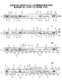
10 第1の基板
11,12 ワイヤ接続用パッド
13 チップ部品
14 ワイヤ
20 第2の基板
21 電極
22 銅コア
23 はんだ被膜
24 露出面
25 空間部
26 銅ボール
30 フラックス不含有導電性ペースト
40 封止樹脂
50A,50B,50C,50D 電子装置
51 はんだボール
62 電子部品
Claims (8)
- 接続用パッドが形成された第1の基板に、チップ部品をワイヤボンディング接続する工程と、
第2の基板の電極接続用パッドに、金属コアにはんだ膜が被膜された電極をはんだ付けする工程と、
前記電極の前記第1の基板に形成された前記接続用パッドと接合される部位を研磨することにより前記はんだ膜を除去し、前記金属コアが露出した平坦な露出面を形成する工程と、
前記第1の基板に形成された前記接続用パッドと前記電極の前記金属コアが露出した部位を、フラックス不含有の導電性接合部材を用いて接合し、前記チップ部品が内蔵されるよう前記第1の基板と前記第2の基板を接合する工程と、
前記第1の基板と前記第2の基板との離間部分に樹脂を充填して前記チップ部品および前記電極を封止する工程と
を有することを特徴とするチップ内蔵基板の製造方法。 - 前記導電性接合部材は、フラックス不含有の導電性ペーストであることを特徴とする請求項1記載のチップ内蔵基板の製造方法。
- 前記金属コアの材質が銅であることを特徴とする請求項1又は2記載のチップ内蔵基板の製造方法。
- 前記導電性ペーストは、フィラーとして銅又は銀を用いていることを特徴とする請求項2記載のチップ内蔵基板の製造方法。
- 接続用パッドが形成された第1の基板に、チップ部品をワイヤボンディング接続する工程と、
第2の基板に設けられた電極接続用パッドに、金属ボールからなり基板面から突出する電極をフラックス不含有導電性ペーストにより接合する工程と、
前記電極の前記第1の基板に形成された前記接続用パッドと接合される部位を研磨処理して平坦化する工程と、
前記第1の基板に形成された前記接続用パッドと前記電極をフラックス不含有の導電性接合部材を用いて接合し、前記チップ部品が内蔵されるよう前記第1の基板と前記第2の基板とを接合する工程と、
前記第1の基板と前記第2の基板との離間部分に樹脂を充填し、前記チップ部品及び前記電極を封止する工程と
を有することを特徴とするチップ内蔵基板の製造方法。 - 前記導電性接合部材は、フラックス不含有の導電性ペーストであることを特徴とする請求項5記載のチップ内蔵基板の製造方法。
- 前記金属ボールが銅ボールであることを特徴とする請求項5又は6記載のチップ内蔵基板の製造方法。
- 前記導電性ペーストは、フィラーとして銅又は銀を用いていることを特徴とする請求項6記載のチップ内蔵基板の製造方法。
Priority Applications (2)
| Application Number | Priority Date | Filing Date | Title |
|---|---|---|---|
| JP2007133948A JP5036397B2 (ja) | 2007-05-21 | 2007-05-21 | チップ内蔵基板の製造方法 |
| US12/123,673 US7754535B2 (en) | 2007-05-21 | 2008-05-20 | Method of manufacturing chip integrated substrate |
Applications Claiming Priority (1)
| Application Number | Priority Date | Filing Date | Title |
|---|---|---|---|
| JP2007133948A JP5036397B2 (ja) | 2007-05-21 | 2007-05-21 | チップ内蔵基板の製造方法 |
Publications (3)
| Publication Number | Publication Date |
|---|---|
| JP2008288490A JP2008288490A (ja) | 2008-11-27 |
| JP2008288490A5 JP2008288490A5 (ja) | 2010-03-11 |
| JP5036397B2 true JP5036397B2 (ja) | 2012-09-26 |
Family
ID=40072816
Family Applications (1)
| Application Number | Title | Priority Date | Filing Date |
|---|---|---|---|
| JP2007133948A Active JP5036397B2 (ja) | 2007-05-21 | 2007-05-21 | チップ内蔵基板の製造方法 |
Country Status (2)
| Country | Link |
|---|---|
| US (1) | US7754535B2 (ja) |
| JP (1) | JP5036397B2 (ja) |
Families Citing this family (5)
| Publication number | Priority date | Publication date | Assignee | Title |
|---|---|---|---|---|
| JP4985623B2 (ja) * | 2008-11-28 | 2012-07-25 | ブラザー工業株式会社 | 配線部材の接続方法、配線部材の製造方法、及び、配線部材 |
| JP2010287710A (ja) * | 2009-06-11 | 2010-12-24 | Renesas Electronics Corp | 半導体装置およびその製造方法 |
| JP2011009514A (ja) | 2009-06-26 | 2011-01-13 | Renesas Electronics Corp | 半導体装置の製造方法 |
| JP5149881B2 (ja) | 2009-09-30 | 2013-02-20 | ルネサスエレクトロニクス株式会社 | 半導体装置の製造方法 |
| US9859200B2 (en) | 2014-12-29 | 2018-01-02 | STATS ChipPAC Pte. Ltd. | Integrated circuit packaging system with interposer support structure mechanism and method of manufacture thereof |
Family Cites Families (10)
| Publication number | Priority date | Publication date | Assignee | Title |
|---|---|---|---|---|
| JP3332308B2 (ja) * | 1995-11-07 | 2002-10-07 | 新光電気工業株式会社 | 半導体装置及びその製造方法 |
| US5994166A (en) * | 1997-03-10 | 1999-11-30 | Micron Technology, Inc. | Method of constructing stacked packages |
| US6406988B1 (en) * | 1998-04-24 | 2002-06-18 | Amerasia International Technology, Inc. | Method of forming fine pitch interconnections employing magnetic masks |
| US6929971B2 (en) * | 2001-04-04 | 2005-08-16 | Texas Instruments Incorporated | Semiconductor device and its manufacturing method |
| TW495943B (en) * | 2001-04-18 | 2002-07-21 | Siliconware Precision Industries Co Ltd | Semiconductor package article with heat sink structure and its manufacture method |
| JP2002353398A (ja) * | 2001-05-25 | 2002-12-06 | Nec Kyushu Ltd | 半導体装置 |
| JP2003069181A (ja) * | 2001-08-28 | 2003-03-07 | Mitsubishi Electric Corp | 電子機器装置及びその製造方法 |
| JP2003347722A (ja) | 2002-05-23 | 2003-12-05 | Ibiden Co Ltd | 多層電子部品搭載用基板及びその製造方法 |
| JPWO2006035528A1 (ja) * | 2004-09-29 | 2008-05-15 | 株式会社村田製作所 | スタックモジュール及びその製造方法 |
| US20070063347A1 (en) * | 2005-09-19 | 2007-03-22 | Taiwan Semiconductor Manufacturing Co., Ltd. | Packages, anisotropic conductive films, and conductive particles utilized therein |
-
2007
- 2007-05-21 JP JP2007133948A patent/JP5036397B2/ja active Active
-
2008
- 2008-05-20 US US12/123,673 patent/US7754535B2/en active Active
Also Published As
| Publication number | Publication date |
|---|---|
| US7754535B2 (en) | 2010-07-13 |
| US20080293236A1 (en) | 2008-11-27 |
| JP2008288490A (ja) | 2008-11-27 |
Similar Documents
| Publication | Publication Date | Title |
|---|---|---|
| JP4864810B2 (ja) | チップ内蔵基板の製造方法 | |
| JP4858541B2 (ja) | 中継基板および電子回路実装構造体 | |
| JP4659262B2 (ja) | 電子部品の実装方法及びペースト材料 | |
| JPWO2001026147A1 (ja) | 半導体装置及びその製造方法、回路基板並びに電子機器 | |
| JP4729963B2 (ja) | 電子部品接続用突起電極とそれを用いた電子部品実装体およびそれらの製造方法 | |
| JP4661122B2 (ja) | 部品実装配線基板および配線基板への部品の実装方法 | |
| CN102612274A (zh) | 配线基板及其制造方法 | |
| JP5036397B2 (ja) | チップ内蔵基板の製造方法 | |
| JP5569676B2 (ja) | 電子部品の実装方法 | |
| JP4051570B2 (ja) | 半導体装置の製造方法 | |
| JP2000277649A (ja) | 半導体装置及びその製造方法 | |
| JP3972209B2 (ja) | 半導体装置及びその製造方法、回路基板並びに電子機器 | |
| JPH0831871A (ja) | 電子部品を表面実装する際に使用する界面封止用フィルム、及び電子部品の表面実装構造 | |
| JP4561969B2 (ja) | 半導体装置 | |
| JP4285140B2 (ja) | 半導体装置の製造方法 | |
| US20250309077A1 (en) | Substrate with embedded electronic component and method of making the same | |
| JP2007035870A (ja) | 半導体装置 | |
| US20250309076A1 (en) | Substrate with embedded electronic component and method of making the same | |
| CN101752335B (zh) | 半导体装置以及半导体装置的制造方法 | |
| JP4591715B2 (ja) | 半導体装置の製造方法 | |
| KR20120047098A (ko) | 패키지 기판용 리드핀과 상기 리드핀을 포함하는 반도체 패키지 인쇄회로기판 및 그 제조방법. | |
| JP2007266640A (ja) | 半導体装置及びその製造方法、回路基板並びに電子機器 | |
| KR100818095B1 (ko) | 플립 칩 패키지 및 그의 형성방법 | |
| CN101355065A (zh) | 具有外部连接端子的半导体器件及其制造方法 | |
| JP4117480B2 (ja) | 半導体装置及びその製造方法、回路基板並びに電子機器 |
Legal Events
| Date | Code | Title | Description |
|---|---|---|---|
| A521 | Request for written amendment filed |
Free format text: JAPANESE INTERMEDIATE CODE: A523 Effective date: 20100125 |
|
| A621 | Written request for application examination |
Free format text: JAPANESE INTERMEDIATE CODE: A621 Effective date: 20100125 |
|
| A977 | Report on retrieval |
Free format text: JAPANESE INTERMEDIATE CODE: A971007 Effective date: 20111020 |
|
| A131 | Notification of reasons for refusal |
Free format text: JAPANESE INTERMEDIATE CODE: A131 Effective date: 20111025 |
|
| A521 | Request for written amendment filed |
Free format text: JAPANESE INTERMEDIATE CODE: A523 Effective date: 20111221 |
|
| TRDD | Decision of grant or rejection written | ||
| A01 | Written decision to grant a patent or to grant a registration (utility model) |
Free format text: JAPANESE INTERMEDIATE CODE: A01 Effective date: 20120626 |
|
| A01 | Written decision to grant a patent or to grant a registration (utility model) |
Free format text: JAPANESE INTERMEDIATE CODE: A01 |
|
| A61 | First payment of annual fees (during grant procedure) |
Free format text: JAPANESE INTERMEDIATE CODE: A61 Effective date: 20120703 |
|
| FPAY | Renewal fee payment (event date is renewal date of database) |
Free format text: PAYMENT UNTIL: 20150713 Year of fee payment: 3 |
|
| R150 | Certificate of patent or registration of utility model |
Ref document number: 5036397 Country of ref document: JP Free format text: JAPANESE INTERMEDIATE CODE: R150 Free format text: JAPANESE INTERMEDIATE CODE: R150 |