JP5028811B2 - 化合物半導体光デバイスを作製する方法 - Google Patents
化合物半導体光デバイスを作製する方法 Download PDFInfo
- Publication number
- JP5028811B2 JP5028811B2 JP2006027398A JP2006027398A JP5028811B2 JP 5028811 B2 JP5028811 B2 JP 5028811B2 JP 2006027398 A JP2006027398 A JP 2006027398A JP 2006027398 A JP2006027398 A JP 2006027398A JP 5028811 B2 JP5028811 B2 JP 5028811B2
- Authority
- JP
- Japan
- Prior art keywords
- mask
- compound semiconductor
- etching
- film
- dielectric mask
- Prior art date
- Legal status (The legal status is an assumption and is not a legal conclusion. Google has not performed a legal analysis and makes no representation as to the accuracy of the status listed.)
- Expired - Fee Related
Links
- 239000004065 semiconductor Substances 0.000 title claims description 98
- 150000001875 compounds Chemical class 0.000 title claims description 74
- 238000000034 method Methods 0.000 title claims description 45
- 230000003287 optical effect Effects 0.000 title claims description 19
- 238000005530 etching Methods 0.000 claims description 79
- 238000001312 dry etching Methods 0.000 claims description 26
- 239000007789 gas Substances 0.000 claims description 22
- 238000004519 manufacturing process Methods 0.000 claims description 20
- VYPSYNLAJGMNEJ-UHFFFAOYSA-N Silicium dioxide Chemical compound O=[Si]=O VYPSYNLAJGMNEJ-UHFFFAOYSA-N 0.000 claims description 18
- 229910052814 silicon oxide Inorganic materials 0.000 claims description 18
- 239000000463 material Substances 0.000 claims description 15
- 150000003377 silicon compounds Chemical class 0.000 claims description 11
- 239000000758 substrate Substances 0.000 claims description 11
- QVGXLLKOCUKJST-UHFFFAOYSA-N atomic oxygen Chemical compound [O] QVGXLLKOCUKJST-UHFFFAOYSA-N 0.000 claims description 8
- 239000001301 oxygen Substances 0.000 claims description 8
- 229910052760 oxygen Inorganic materials 0.000 claims description 8
- BOTDANWDWHJENH-UHFFFAOYSA-N Tetraethyl orthosilicate Chemical compound CCO[Si](OCC)(OCC)OCC BOTDANWDWHJENH-UHFFFAOYSA-N 0.000 claims description 6
- 238000005229 chemical vapour deposition Methods 0.000 claims description 6
- 239000004215 Carbon black (E152) Substances 0.000 claims description 4
- BLRPTPMANUNPDV-UHFFFAOYSA-N Silane Chemical compound [SiH4] BLRPTPMANUNPDV-UHFFFAOYSA-N 0.000 claims description 4
- 229930195733 hydrocarbon Natural products 0.000 claims description 4
- 150000002430 hydrocarbons Chemical class 0.000 claims description 4
- 150000001282 organosilanes Chemical class 0.000 claims description 4
- 229910000077 silane Inorganic materials 0.000 claims description 4
- 238000009616 inductively coupled plasma Methods 0.000 claims description 3
- UFHFLCQGNIYNRP-UHFFFAOYSA-N Hydrogen Chemical compound [H][H] UFHFLCQGNIYNRP-UHFFFAOYSA-N 0.000 claims description 2
- 238000000151 deposition Methods 0.000 claims description 2
- 239000001257 hydrogen Substances 0.000 claims description 2
- 229910052739 hydrogen Inorganic materials 0.000 claims description 2
- 239000002356 single layer Substances 0.000 claims description 2
- 239000010408 film Substances 0.000 description 77
- 238000001020 plasma etching Methods 0.000 description 15
- 230000008569 process Effects 0.000 description 11
- 238000010586 diagram Methods 0.000 description 9
- 239000010410 layer Substances 0.000 description 9
- 229910004298 SiO 2 Inorganic materials 0.000 description 7
- 239000002184 metal Substances 0.000 description 6
- 229910052751 metal Inorganic materials 0.000 description 6
- 239000010409 thin film Substances 0.000 description 5
- 239000013078 crystal Substances 0.000 description 4
- 230000007423 decrease Effects 0.000 description 4
- 238000002230 thermal chemical vapour deposition Methods 0.000 description 4
- 230000000903 blocking effect Effects 0.000 description 3
- 238000011109 contamination Methods 0.000 description 3
- 238000000206 photolithography Methods 0.000 description 3
- 238000007740 vapor deposition Methods 0.000 description 3
- IJGRMHOSHXDMSA-UHFFFAOYSA-N Atomic nitrogen Chemical compound N#N IJGRMHOSHXDMSA-UHFFFAOYSA-N 0.000 description 2
- 229910001218 Gallium arsenide Inorganic materials 0.000 description 2
- 238000013459 approach Methods 0.000 description 2
- 230000008859 change Effects 0.000 description 2
- 238000005253 cladding Methods 0.000 description 2
- 229910001873 dinitrogen Inorganic materials 0.000 description 2
- 230000008034 disappearance Effects 0.000 description 2
- 229910052736 halogen Inorganic materials 0.000 description 2
- 150000002367 halogens Chemical class 0.000 description 2
- 238000010438 heat treatment Methods 0.000 description 2
- 239000005416 organic matter Substances 0.000 description 2
- 230000009467 reduction Effects 0.000 description 2
- -1 CH 4 gas can be used Chemical class 0.000 description 1
- 229910000530 Gallium indium arsenide Inorganic materials 0.000 description 1
- 238000004380 ashing Methods 0.000 description 1
- 239000002131 composite material Substances 0.000 description 1
- 230000006866 deterioration Effects 0.000 description 1
- 238000005516 engineering process Methods 0.000 description 1
- 238000012986 modification Methods 0.000 description 1
- 230000004048 modification Effects 0.000 description 1
- 238000005268 plasma chemical vapour deposition Methods 0.000 description 1
- 229920000642 polymer Polymers 0.000 description 1
- 239000002994 raw material Substances 0.000 description 1
- 238000004528 spin coating Methods 0.000 description 1
- 238000004544 sputter deposition Methods 0.000 description 1
- 238000001947 vapour-phase growth Methods 0.000 description 1
Images


Landscapes
- Drying Of Semiconductors (AREA)
- Semiconductor Lasers (AREA)
Description
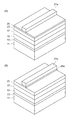
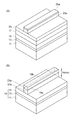
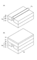
H≧h/3
の関係を満たす誘電体マスク膜が形成される。
ECRの高周波電力:50〜300(W)
バイアス電力 :50〜300(W)
エッチング圧力 :0.5〜5 (Pa)
CH4ガス流量 :20〜50 (sccm)
H2ガス流量 :0〜50 (sccm)
である。
基板11:n型InP基板
n型III―V化合物半導体膜13:SiドープInP(n型クラッド)
活性領域15:InGaAsPからなる量子井戸構造
埋め込み領域29:FeドープInP(電流ブロック)
p型III―V化合物半導体膜31:ZnドープInP(p型クラッド)
p型III―V化合物半導体コンタクト膜33:ZnドープInGaAs
である。
H≧h/3
の関係を満たすことが好ましい。この方法によれば、エッチング量が大きく高いメサ形状を作製することができる。例えば、SiO2からなる誘電体マスクの高さが約1μmであるとき、メサ側面の垂直性を保ちながらInP半導体を3.5μm程度の深さまでエッチングできる。誘電体マスクの厚みHは、エッチングにより作製されるべきメサの深さhの3倍程度にすることが好ましい。これにより、ドライエッチング時の横方向へのマスク減退が無くなるので、垂直なエッチング側面を有するメサを作製可能となる。また、横方向のマスク減退を防ぐことができるので、マスク幅に従ったエッチング形状の実現が可能となりエッチング幅の制御性が向上する。
Claims (4)
- 化合物半導体光デバイスを作製する方法であって、
基板上に、III−V化合物半導体から成る活性領域を含む化合物半導体領域を形成する工程と、
有機シラン系原料および酸素原料を含む成膜ガスを供給して、シリコン化合物からなる誘電体マスク膜を前記化合物半導体領域上に誘導結合プラズマ−化学的気相成長法で堆積する工程と、
前記誘電体マスク膜にパターンを形成して誘電体マスクを形成する工程と、
前記誘電体マスクを用いて、前記化合物半導体領域のドライエッチングを行って、メサ高さhが3.5μm以上のメサ形状の化合物半導体領域を形成する工程とを備え、
前記ドライエッチングは、バイアス電力を供給し炭化水素と水素の混合ガスを用いたRIEエッチングであり、
前記誘電体マスク膜は、前記メサ形状の化合物半導体領域を形成する工程後の該化合物半導体のメサ高さhとの間に前記誘電体マスクの厚みHがH≧h/3の関係を満しており、
前記エッチングにおいて、前記誘電体マスクの側面と上面によるマスクエッジの変形が前記エッチングのスパッタ成分により引き起こされ、該マスクエッジに傾斜面が形成され、
前記誘電体マスクが単層のシリコン化合物からなる、ことを特徴とする方法。 - 前記バイアス電力は50〜300Wであり、
前記RIEエッチングはECR−RIEエッチングである、ことを特徴とする請求項1に記載された方法。 - 前記有機シラン系原料はTEOSを含み、
前記酸素原料は酸素分子を含み、
前記誘電体マスクの材料はシリコン酸化物からなる、請求項1または請求項2に記載された方法。 - 前記炭化水素はCH 4 を含む、請求項1〜請求項3のいずれか一項に記載された方法。
Priority Applications (1)
| Application Number | Priority Date | Filing Date | Title |
|---|---|---|---|
| JP2006027398A JP5028811B2 (ja) | 2006-02-03 | 2006-02-03 | 化合物半導体光デバイスを作製する方法 |
Applications Claiming Priority (1)
| Application Number | Priority Date | Filing Date | Title |
|---|---|---|---|
| JP2006027398A JP5028811B2 (ja) | 2006-02-03 | 2006-02-03 | 化合物半導体光デバイスを作製する方法 |
Publications (2)
| Publication Number | Publication Date |
|---|---|
| JP2007208134A JP2007208134A (ja) | 2007-08-16 |
| JP5028811B2 true JP5028811B2 (ja) | 2012-09-19 |
Family
ID=38487309
Family Applications (1)
| Application Number | Title | Priority Date | Filing Date |
|---|---|---|---|
| JP2006027398A Expired - Fee Related JP5028811B2 (ja) | 2006-02-03 | 2006-02-03 | 化合物半導体光デバイスを作製する方法 |
Country Status (1)
| Country | Link |
|---|---|
| JP (1) | JP5028811B2 (ja) |
Families Citing this family (1)
| Publication number | Priority date | Publication date | Assignee | Title |
|---|---|---|---|---|
| JP4985411B2 (ja) * | 2008-01-08 | 2012-07-25 | 住友電気工業株式会社 | 半導体光素子を作製する方法 |
Family Cites Families (9)
| Publication number | Priority date | Publication date | Assignee | Title |
|---|---|---|---|---|
| US5431770A (en) * | 1993-10-13 | 1995-07-11 | At&T Corp. | Transistor gate formation |
| JPH07153595A (ja) * | 1993-11-26 | 1995-06-16 | Canon Inc | 有磁場誘導結合プラズマ処理装置 |
| JPH08288272A (ja) * | 1995-04-18 | 1996-11-01 | Sony Corp | ヘリコン波プラズマcvd方法 |
| JP3641866B2 (ja) * | 1996-02-22 | 2005-04-27 | ソニー株式会社 | 半導体装置の製造方法 |
| JPH1197799A (ja) * | 1997-09-22 | 1999-04-09 | Mitsubishi Electric Corp | 半導体装置の製造方法 |
| US6020091A (en) * | 1997-09-30 | 2000-02-01 | Siemens Aktiengesellschaft | Hard etch mask |
| JPH11135478A (ja) * | 1997-10-27 | 1999-05-21 | Asahi Kasei Micro Syst Co Ltd | 半導体装置の製造方法 |
| JP3994362B2 (ja) * | 1998-09-08 | 2007-10-17 | 富士通株式会社 | 化合物半導体装置の製造方法 |
| JP2004281815A (ja) * | 2003-03-17 | 2004-10-07 | Sumitomo Electric Ind Ltd | エッチング方法 |
-
2006
- 2006-02-03 JP JP2006027398A patent/JP5028811B2/ja not_active Expired - Fee Related
Also Published As
| Publication number | Publication date |
|---|---|
| JP2007208134A (ja) | 2007-08-16 |
Similar Documents
| Publication | Publication Date | Title |
|---|---|---|
| JP3729210B2 (ja) | 半導体装置の製造方法 | |
| CN108233175A (zh) | 一种掩埋AlGaInAs DFB激光器的制作方法 | |
| US20120058582A1 (en) | Method for etching insulating film and method for manufacturing semiconductor optical device | |
| JP2010192888A (ja) | 半導体レーザの製造方法 | |
| CN107437497A (zh) | 半导体器件的形成方法 | |
| JP5028811B2 (ja) | 化合物半導体光デバイスを作製する方法 | |
| US8357555B2 (en) | Method for producing semiconductor optical device | |
| JP5531610B2 (ja) | 半導体レーザ素子の製造方法 | |
| JP4985411B2 (ja) | 半導体光素子を作製する方法 | |
| JP5211728B2 (ja) | 半導体光素子を作製する方法 | |
| JP4537549B2 (ja) | 化合物半導体装置の製造方法 | |
| JP5076713B2 (ja) | 化合物半導体光デバイスを作製する方法 | |
| JP2010267674A (ja) | Iii−v化合物半導体光素子を作製する方法 | |
| JP2007184491A (ja) | 分布帰還型半導体レーザ | |
| JP2017011168A (ja) | 半導体受光素子を作製する方法 | |
| JP4350227B2 (ja) | 半導体結晶成長方法 | |
| JP2009129943A (ja) | 窒化物半導体装置とその製造方法 | |
| JP5239544B2 (ja) | 半導体光素子を作製する方法 | |
| JP7359333B1 (ja) | 光半導体装置およびその製造方法 | |
| JP5108687B2 (ja) | 光半導体装置及びその製造方法 | |
| JP5239543B2 (ja) | 半導体光素子を作製する方法 | |
| CN119481956A (zh) | 一种eml激光器及空气桥的制备方法 | |
| CN115210976B (zh) | 半导体装置以及半导体装置的制造方法 | |
| JP2009177076A (ja) | 半導体素子を作製する方法 | |
| CN120676733A (zh) | 一种硅基锗外延窗口结构的制备方法及半导体器件 |
Legal Events
| Date | Code | Title | Description |
|---|---|---|---|
| A621 | Written request for application examination |
Free format text: JAPANESE INTERMEDIATE CODE: A621 Effective date: 20081224 |
|
| A977 | Report on retrieval |
Free format text: JAPANESE INTERMEDIATE CODE: A971007 Effective date: 20090422 |
|
| A131 | Notification of reasons for refusal |
Free format text: JAPANESE INTERMEDIATE CODE: A131 Effective date: 20110719 |
|
| A521 | Written amendment |
Free format text: JAPANESE INTERMEDIATE CODE: A523 Effective date: 20110916 |
|
| TRDD | Decision of grant or rejection written | ||
| A01 | Written decision to grant a patent or to grant a registration (utility model) |
Free format text: JAPANESE INTERMEDIATE CODE: A01 Effective date: 20120529 |
|
| A01 | Written decision to grant a patent or to grant a registration (utility model) |
Free format text: JAPANESE INTERMEDIATE CODE: A01 |
|
| A61 | First payment of annual fees (during grant procedure) |
Free format text: JAPANESE INTERMEDIATE CODE: A61 Effective date: 20120611 |
|
| R150 | Certificate of patent or registration of utility model |
Free format text: JAPANESE INTERMEDIATE CODE: R150 |
|
| FPAY | Renewal fee payment (event date is renewal date of database) |
Free format text: PAYMENT UNTIL: 20150706 Year of fee payment: 3 |
|
| R250 | Receipt of annual fees |
Free format text: JAPANESE INTERMEDIATE CODE: R250 |
|
| LAPS | Cancellation because of no payment of annual fees |