JP5028811B2 - Method for fabricating compound semiconductor optical device - Google Patents
Method for fabricating compound semiconductor optical device Download PDFInfo
- Publication number
- JP5028811B2 JP5028811B2 JP2006027398A JP2006027398A JP5028811B2 JP 5028811 B2 JP5028811 B2 JP 5028811B2 JP 2006027398 A JP2006027398 A JP 2006027398A JP 2006027398 A JP2006027398 A JP 2006027398A JP 5028811 B2 JP5028811 B2 JP 5028811B2
- Authority
- JP
- Japan
- Prior art keywords
- mask
- compound semiconductor
- etching
- film
- dielectric mask
- Prior art date
- Legal status (The legal status is an assumption and is not a legal conclusion. Google has not performed a legal analysis and makes no representation as to the accuracy of the status listed.)
- Expired - Fee Related
Links
- 239000004065 semiconductor Substances 0.000 title claims description 98
- 150000001875 compounds Chemical class 0.000 title claims description 74
- 238000000034 method Methods 0.000 title claims description 45
- 230000003287 optical effect Effects 0.000 title claims description 19
- 238000005530 etching Methods 0.000 claims description 79
- 238000001312 dry etching Methods 0.000 claims description 26
- 239000007789 gas Substances 0.000 claims description 22
- 238000004519 manufacturing process Methods 0.000 claims description 20
- VYPSYNLAJGMNEJ-UHFFFAOYSA-N Silicium dioxide Chemical compound O=[Si]=O VYPSYNLAJGMNEJ-UHFFFAOYSA-N 0.000 claims description 18
- 229910052814 silicon oxide Inorganic materials 0.000 claims description 18
- 239000000463 material Substances 0.000 claims description 15
- 150000003377 silicon compounds Chemical class 0.000 claims description 11
- 239000000758 substrate Substances 0.000 claims description 11
- QVGXLLKOCUKJST-UHFFFAOYSA-N atomic oxygen Chemical compound [O] QVGXLLKOCUKJST-UHFFFAOYSA-N 0.000 claims description 8
- 239000001301 oxygen Substances 0.000 claims description 8
- 229910052760 oxygen Inorganic materials 0.000 claims description 8
- BOTDANWDWHJENH-UHFFFAOYSA-N Tetraethyl orthosilicate Chemical compound CCO[Si](OCC)(OCC)OCC BOTDANWDWHJENH-UHFFFAOYSA-N 0.000 claims description 6
- 238000005229 chemical vapour deposition Methods 0.000 claims description 6
- 239000004215 Carbon black (E152) Substances 0.000 claims description 4
- BLRPTPMANUNPDV-UHFFFAOYSA-N Silane Chemical compound [SiH4] BLRPTPMANUNPDV-UHFFFAOYSA-N 0.000 claims description 4
- 229930195733 hydrocarbon Natural products 0.000 claims description 4
- 150000002430 hydrocarbons Chemical class 0.000 claims description 4
- 150000001282 organosilanes Chemical class 0.000 claims description 4
- 229910000077 silane Inorganic materials 0.000 claims description 4
- 238000009616 inductively coupled plasma Methods 0.000 claims description 3
- UFHFLCQGNIYNRP-UHFFFAOYSA-N Hydrogen Chemical compound [H][H] UFHFLCQGNIYNRP-UHFFFAOYSA-N 0.000 claims description 2
- 238000000151 deposition Methods 0.000 claims description 2
- 239000001257 hydrogen Substances 0.000 claims description 2
- 229910052739 hydrogen Inorganic materials 0.000 claims description 2
- 239000002356 single layer Substances 0.000 claims description 2
- 239000010408 film Substances 0.000 description 77
- 238000001020 plasma etching Methods 0.000 description 15
- 230000008569 process Effects 0.000 description 11
- 238000010586 diagram Methods 0.000 description 9
- 239000010410 layer Substances 0.000 description 9
- 229910004298 SiO 2 Inorganic materials 0.000 description 7
- 239000002184 metal Substances 0.000 description 6
- 229910052751 metal Inorganic materials 0.000 description 6
- 239000010409 thin film Substances 0.000 description 5
- 239000013078 crystal Substances 0.000 description 4
- 230000007423 decrease Effects 0.000 description 4
- 238000002230 thermal chemical vapour deposition Methods 0.000 description 4
- 230000000903 blocking effect Effects 0.000 description 3
- 238000011109 contamination Methods 0.000 description 3
- 238000000206 photolithography Methods 0.000 description 3
- 238000007740 vapor deposition Methods 0.000 description 3
- IJGRMHOSHXDMSA-UHFFFAOYSA-N Atomic nitrogen Chemical compound N#N IJGRMHOSHXDMSA-UHFFFAOYSA-N 0.000 description 2
- 229910001218 Gallium arsenide Inorganic materials 0.000 description 2
- 238000013459 approach Methods 0.000 description 2
- 230000008859 change Effects 0.000 description 2
- 238000005253 cladding Methods 0.000 description 2
- 229910001873 dinitrogen Inorganic materials 0.000 description 2
- 230000008034 disappearance Effects 0.000 description 2
- 229910052736 halogen Inorganic materials 0.000 description 2
- 150000002367 halogens Chemical class 0.000 description 2
- 238000010438 heat treatment Methods 0.000 description 2
- 239000005416 organic matter Substances 0.000 description 2
- 230000009467 reduction Effects 0.000 description 2
- -1 CH 4 gas can be used Chemical class 0.000 description 1
- 229910000530 Gallium indium arsenide Inorganic materials 0.000 description 1
- 238000004380 ashing Methods 0.000 description 1
- 239000002131 composite material Substances 0.000 description 1
- 230000006866 deterioration Effects 0.000 description 1
- 238000005516 engineering process Methods 0.000 description 1
- 238000012986 modification Methods 0.000 description 1
- 230000004048 modification Effects 0.000 description 1
- 238000005268 plasma chemical vapour deposition Methods 0.000 description 1
- 229920000642 polymer Polymers 0.000 description 1
- 239000002994 raw material Substances 0.000 description 1
- 238000004528 spin coating Methods 0.000 description 1
- 238000004544 sputter deposition Methods 0.000 description 1
- 238000001947 vapour-phase growth Methods 0.000 description 1
Images


Landscapes
- Drying Of Semiconductors (AREA)
- Semiconductor Lasers (AREA)
Description
本発明は、化合物半導体光デバイスを作製する方法に関する。 The present invention relates to a method of manufacturing a compound semiconductor optical device.
特許文献1には、化合物半導体のエッチング方法および半導体レーザ素子の製造方法が記載されている。このエッチング方法によれば、化合物半導体のドライエッチングにおいて、垂直で平滑なエッチング面が提供される。具体的には、III−V族化合物半導体またはII−VI族化合物半導体は、約1010cm−3以上の密度のプラズマを発生するプラズマ源を備えたドライエッチング装置に、ハロゲン元素を含むガスと窒素ガスとの混合ガスを供給して、ドライエッチングされる。(ハロゲン元素を含むガスの流量)/(窒素ガスの流量)は1以上でであり、エッチング反応中の圧力は、約1mTorrまたは1mTorr以上である。
非特許文献1には、化合物半導体デバイス製造においてドライエッチングによりメサ形状を得る方法が記載されている。メサ形状を得る方法として2つの方法が説明されている。一方の方法では、ドライエッチングのためにSiN、SiO2等の絶縁膜を厚さ0.3μmからなる薄膜マスクを用いる。他の方法では、ドライエッチングのために多層マスクを用いる。多層マスクは、例えば、200〜300℃で熱処理されて硬化した1.5μm厚のレジスト(下層)、Ti等からなる0.1μm厚のメタルマスク(中間層)からなる。
非特許文献1に記載された薄膜マスクを用いるエッチング方法では、エッチング中に、半導体領域がエッチングにより加工されるだけでなく、マスクの形状もエッチングの進行と共に変化する。このため、エッチングされた半導体領域の形状が、裾を引くリッジ形状になる。このエッチングでは、エッチングマスクとして厚さ0.3μm程度のSiN、SiO2等の絶縁膜を用いて反応性イオンエッチング(RIE)を行う。RIE法では、エッチングが進行するにつれて、マスク側面とマスク上面とからなるエッジから進行する(マスクエッジの変形)。この変形はスパッタ成分により引き起こされマスク上部のエッジから45度の角度方向に進み、これによりマスク上部および側面と約135度の角度を成す傾斜面が形成される。マスクの変形は、垂直方向のエッチング速度の8〜10倍の消失速度で進む。マスクの変形により側面が消失した後は、エッチングの進行に伴いマスク幅が小さくなる(マスク幅の後退)。ドライエッチング中にマスク幅が縮小すると、メサ側面が裾を引くようになり、結果的にメサ幅は基板に近づくにつれて広くなる。メサのエッチング角度をほぼ垂直に維持しながらドライエッチングを行うことができない。つまり、ドライエッチングにより直角に近い段差を形成することができない。
In the etching method using the thin film mask described in
エッチングマスクとして厚さ1.5μm程度の硬化レジスト、厚さ0.1μm程度のTi等メタルマスクの複合マスクを用いてエッチングを行う。この方法では、マスクとして使用した下層レジストがエッチングによりポリマー化してメサ側面に付着する。この付着したポリマーは、埋め込みエピ成長工程において、有機物コンタミネーションの原因となる。付着有機物は、高温ベーク工程および反応性イオンエッチング工程を経ているので、容易に除去できない。また、発明者の知見によれば、付着有機物は、埋め込みモフォロジーの悪化を引き起こす。これ故に、この方法は、汚染の少ない清浄表面が必要とされる工程、例えば、半導体レーザの活性層を含むメサをドライエッチングで形成する工程、では使用できない。 Etching is performed using a composite mask of a hard mask having a thickness of about 1.5 μm and a metal mask such as Ti having a thickness of about 0.1 μm as an etching mask. In this method, the lower layer resist used as a mask is polymerized by etching and adheres to the side surface of the mesa. The attached polymer causes organic contamination in the buried epi growth process. The attached organic matter cannot be easily removed because it has undergone a high temperature baking step and a reactive ion etching step. Further, according to the inventor's knowledge, the attached organic matter causes deterioration of the embedded morphology. Therefore, this method cannot be used in a process where a clean surface with little contamination is required, for example, a process of forming a mesa including an active layer of a semiconductor laser by dry etching.
本発明は、このような事情を鑑みてなされたものであり、エッチング中にマスク幅の大きな変化を生じることがない、化合物半導体光デバイスを作製する方法を提供することを目的とする。 The present invention has been made in view of such circumstances, and an object of the present invention is to provide a method of manufacturing a compound semiconductor optical device that does not cause a large change in mask width during etching.
本発明の一側面は、化合物半導体光デバイスを作製する方法に係る。この方法は、(a)有機シラン系原料および酸素原料を含む成膜ガスを供給して、シリコン化合物からなる誘電体マスク膜を化合物半導体領域上に誘導結合プラズマ−化学的気相成長法で堆積する工程と、(b)前記誘電体マスク膜にパターンを形成して誘電体マスクを形成する工程と、(c)前記誘電体マスクを用いて、前記化合物半導体領域のドライエッチングを行ってメサ高さhが3.5μm以上のメサ形状の化合物半導体領域を形成する工程とを備え、前記誘電体マスクが単層のシリコン化合物からなる。 One aspect of the present invention relates to a method of fabricating a compound semiconductor optical device. In this method, (a) a film forming gas containing an organosilane source material and an oxygen source material is supplied, and a dielectric mask film made of a silicon compound is deposited on the compound semiconductor region by inductively coupled plasma-chemical vapor deposition. (B) forming a dielectric mask by forming a pattern on the dielectric mask film; and (c) performing dry etching on the compound semiconductor region using the dielectric mask to increase the mesa height. Forming a mesa-shaped compound semiconductor region having a thickness h of 3.5 μm or more, and the dielectric mask is made of a single-layer silicon compound.
この発明によれば、誘電体マスクのためのシリコン化合物が誘導結合プラズマ−化学的気相成長法で形成されるので、例えば1マイクロメートル以上の厚みを有する厚膜で単層の誘電体マスクを得ることができる。厚膜の誘電体マスクを用いて化合物半導体領域のドライエッチングを行うので、メサ高さが3.5μm以上の深いメサを加工する場合でも、エッチング中にマスクエッジの消失が生じてもマスク幅が小さくなることはない。これ故に、所望のメサ形状の化合物半導体領域を形成できる。 According to the present invention, since the silicon compound for the dielectric mask is formed by inductively coupled plasma-chemical vapor deposition, a thick dielectric film having a thickness of, for example, 1 micrometer or more is formed. Obtainable. Since the compound semiconductor region is dry-etched using a thick dielectric mask, even if a deep mesa with a mesa height of 3.5 μm or more is processed, the mask width can be increased even if the mask edge disappears during etching. It will never get smaller. Therefore, a desired mesa-shaped compound semiconductor region can be formed.
本発明に係る方法では、前記誘電体マスクの厚みHが、メサ形状加工した化合物半導体のメサ高さhとの間に、
H≧h/3
の関係を満たす誘電体マスク膜が形成される。
In the method according to the present invention, the thickness H of the dielectric mask is between the mesa height h of the mesa-shaped processed compound semiconductor,
H ≧ h / 3
A dielectric mask film satisfying the above relationship is formed.
この発明によれば、メサ形状の化合物半導体領域を形成する前記工程においてドライエッチングが進行するにつれて、前記誘電体マスクが該マスクの上面のエッジから後退すると共に、この後退に伴い該マスクの側面の高さHMが小さくなる場合でも、エッチング量が大きく高いメサ形状を作製することができる。 According to the present invention, as the dry etching progresses in the step of forming the mesa-shaped compound semiconductor region, the dielectric mask recedes from the edge of the upper surface of the mask, and the side surface of the mask accompanies the receding. Even when the height HM is small, a mesa shape having a large etching amount and a high etching amount can be produced.
本発明に係る方法では、前記有機シラン系原料はTEOS(テトラエトキシシラン)を含み、前記酸素原料は酸素分子を含み、前記誘電体マスクの材料はシリコン酸化物からなることが好ましい。 In the method according to the present invention, it is preferable that the organosilane-based material includes TEOS (tetraethoxysilane), the oxygen material includes oxygen molecules, and the dielectric mask material includes silicon oxide.
この方法によれば、膜厚を厚くしても膜中の応力が小さいシリコン酸化物を誘電体マスクのために形成できる。 According to this method, even if the film thickness is increased, silicon oxide having a small stress in the film can be formed for the dielectric mask.
本発明に係る方法では、前記ドライエッチングのためのガスは炭化水素を含むことが好ましい。この方法によれば、化合物半導体のドライエッチングが可能であり、所望のメサ形状の化合物半導体領域を形成できる。 In the method according to the present invention, the dry etching gas preferably contains a hydrocarbon. According to this method, the compound semiconductor can be dry-etched, and a desired mesa-shaped compound semiconductor region can be formed.
本発明の上記の目的および他の目的、特徴、並びに利点は、添付図面を参照して進められる本発明の好適な実施の形態の以下の詳細な記述から、より容易に明らかになる。 The above and other objects, features, and advantages of the present invention will become more readily apparent from the following detailed description of preferred embodiments of the present invention, which proceeds with reference to the accompanying drawings.
以上説明したように、本発明によれば、エッチング中にマスク幅の大きな変化を生じることがない、化合物半導体光デバイスを作製する方法が提供される。 As described above, according to the present invention, a method for producing a compound semiconductor optical device that does not cause a large change in mask width during etching is provided.
本発明の知見は、例示として示された添付図面を参照して以下の詳細な記述を考慮することによって容易に理解できる。引き続いて、添付図面を参照しながら、本発明の化合物半導体光デバイスを作製する方法に係る実施の形態を説明する。可能な場合には、同一の部分には同一の符号を付する。 The knowledge of the present invention can be easily understood by considering the following detailed description with reference to the accompanying drawings shown as examples. Subsequently, an embodiment relating to a method for producing a compound semiconductor optical device of the present invention will be described with reference to the accompanying drawings. Where possible, the same parts are denoted by the same reference numerals.
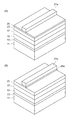
図1(A)は、化合物半導体光デバイスを作製する方法における結晶成長工程を示す模式図である。InP半導体からなる表面11aを有する基板11を準備する。基板11は導電性を示しており、例えば、n型InP半導体からなることができる。基板11上に、III―V化合物半導体から成る活性領域13を成長する。活性領域13は、例えばバルク構造、単一量子井戸構造、多重量子井戸構造といった構造を有することができる。次いで、活性領域13上に、III―V化合物半導体膜15を成長する。III―V化合物半導体膜15は、例えばp型InP半導体からなることができる。活性領域13およびIII―V化合物半導体膜15の成長は、例えば有機金属気相成長炉を用いて行われる。
FIG. 1A is a schematic view showing a crystal growth step in a method for producing a compound semiconductor optical device. A
図1(B)は、誘電体マスクのための多層構造および誘電体マスク膜を形成するマスク作製工程を示す図面である。誘電体マスク膜17をIII―V化合物半導体膜15上に形成する。誘電体マスク膜17は、有機シラン系原料および酸素原料を含む成膜ガスを供給して誘導結合プラズマ気相成長(ICP−CVD)装置を用いて形成される。好ましく、誘電体マスク膜17はシリコン化合物からなり、シリコン化合物は例えばシリコン酸化物等を含むことができる。誘電体マスク膜17の厚みHFILMは1マイクロメートル以上である。次いで、誘電体マスク膜17にパターンを形成して誘電体マスクを形成する。有機シラン系原料としては、例えばTEOS等を用いることができ、また酸素原料としては例えばO2等を用いることができる。
FIG. 1B is a drawing showing a mask manufacturing process for forming a multilayer structure for a dielectric mask and a dielectric mask film. A
SiH4といったシラン系ガスを使用したプラズマエンハース気相成長法(PE−CVD)によるSiN膜、および熱気相成長法(熱CVD)によるSiO2膜は応力制御が不可能であるので、その膜の厚み大きくすることが不可能である。厚いSiN膜およびSiO2膜には、割れが発生する。しかしながら、ICP−CVD装置を用いて誘電体マスク膜17を形成するので、膜の応力の制御が可能になる。これ故に、たとえば1マイクロメートル以上の厚みを有する厚膜のマスク膜が利用可能になる。応力の制御が可能なマスク膜は、TEOSといった有機シラン系原料を用いICP−CVD法で形成できるシリコン酸化膜である。これ故に、半導体デバイスの作製において汚染が生じることはない。
Since an SiN film by plasma enhanced vapor deposition (PE-CVD) using a silane-based gas such as SiH 4 and an SiO 2 film by thermal vapor deposition (thermal CVD) cannot be stress-controlled, the films It is impossible to increase the thickness. Cracks occur in the thick SiN film and SiO 2 film. However, since the
この誘電体マスクの形成のための一例を説明する。まず、誘電体マスク膜17上に第1のエッチングマスク材19を形成する。好適な例では、第1のエッチング材19は多層構造21を有することができる。多層構造21は第1〜第3の層からなる。第1の層は例えば硬化されたレジスト膜23であり、具体的には、硬化レジスト膜23は、レジストを塗布して1マイクロメートル以上のレジスト膜を形成した後に、摂氏100度以上の温度で熱処理して形成される。第2の膜は例えばシリコン化合物膜25、Ti、Crなどの金属膜、具体的にはスパッタなどの低温で成膜できる金属薄膜等であり、具体的には、スピンコート法で0.1マイクロメートル程度のシリコン酸化物薄膜を形成される。第3の膜27は、例えば感光性レジスト膜であり、具体的には、感光性レジストをシリコン化合物膜25上に塗布して形成される。
An example for forming this dielectric mask will be described. First, a first
図2(A)は、フォトリソグラフィ法を用いてレジストマスクを形成する工程を示す図面である。化合物半導体光デバイスのための光学マスクを用いて感光性レジスト膜27を露光した後に、露光されたレジスト膜を現像する。図2(A)を参照すると、フォトリソグラフィ法でレジストマスク27aが形成される。本実施例では、半導体レーザのメサストライプを作製するためのパターンを有するマスクが形成される。
FIG. 2A illustrates a step of forming a resist mask using a photolithography method. After exposing the photosensitive resist
図2(B)に示されるように、レジストマスク27aを用いてシリコン酸化物薄膜をエッチングして、シリコン酸化物マスク25aを作製する。本実施例では、このエッチングは、例えばRIEエッチング装置を用いて行われる。エッチングガスは、例えばCF4ガスを用いることができる。これにより、エッチング中に十分な選択比を維持できる。この結果、メサストライプを作製するためのパターンが転写されたシリコン酸化物マスク25aが得られる。この後に、レジストマスク27aを除去する。この除去は、例えばO2ガスによるプラズマアッシングにより行われる。
As shown in FIG. 2B, the silicon oxide thin film is etched using the resist
図3(A)は、シリコン酸化物マスクを用いて硬化レジストマスクを形成する工程を示す図面である。シリコン酸化物マスク25aを用いて硬化レジスト膜23をエッチングして硬化レジストマスク23aを形成する。本実施例では、このエッチングは、例えばRIEエッチング装置を用いて行われる。エッチングガスは、例えばO2ガスを用いることができる。これにより、十分な選択比を維持できる。この結果、メサストライプを作製するためのパターンが転写された硬化レジストマスク23aが得られる。この後に、シリコン酸化物マスク25aを除去する。この除去は、例えばCHF3ガスを用いたRIEエッチングにより行われる。
FIG. 3A is a diagram illustrating a process of forming a cured resist mask using a silicon oxide mask. The cured resist
図3(B)は、誘電体マスク膜にパターンを形成して誘電体マスクを形成する工程を示す図面である。硬化レジストマスク23aを用いて誘電体マスク膜17をエッチングする。本実施例では、このエッチングは、例えばRIEエッチング装置を用いて行われる。エッチングガスは、例えばCHF3ガスを用いることができる。これにより、十分な選択比を維持できる。この結果、メサストライプを作製するためのパターンが転写された誘電体マスク17aが得られる。誘電体マスク17aの厚みHMASKは、1マイクロメートル以上である。この後に、硬化レジストマスク23aを除去する。この除去は、例えばO2ガスによるRIEエッチング装置により行われる。また、上記のレジストマスク27a、およびシリコン酸化物マスク25aの除去は、この硬化レジストマスク23aを除去する際、一度に除去することもできるので、このレジストマスク27aの除去工程、およびシリコン酸化物マスク25aの除去工程を省略することもできる。
FIG. 3B is a drawing showing a process of forming a dielectric mask by forming a pattern on the dielectric mask film. The
誘電体マスク膜上に直接に感光レジストマスクを形成すると、感光レジストマスクのストライプパターンの断面形状が台形になる。この転写されたストライプパターンの幅の精度の誤差が大きくなる。3層マスクを用いると、感光レジストマスクのストライプパターンの断面形状が矩形になり、反応性イオンエッチングを用いた場合、パターンの転写精度を向上させることができる。 When a photosensitive resist mask is formed directly on the dielectric mask film, the cross-sectional shape of the stripe pattern of the photosensitive resist mask becomes a trapezoid. An error in the accuracy of the width of the transferred stripe pattern increases. When a three-layer mask is used, the cross-sectional shape of the stripe pattern of the photosensitive resist mask becomes rectangular, and when reactive ion etching is used, the pattern transfer accuracy can be improved.
図4(A)および図4(B)は、誘電体マスクを用いて、化合物半導体領域のドライエッチングを行ってメサ形状の化合物半導体領域を形成する工程を示す図面である。誘電体マスク17aを用いて、化合物半導体領域15、13、11のドライエッチングを行う。本実施例では、このエッチングは、例えばECR−RIEエッチング装置を用いて行われる。エッチングガスは、例えばCH4ガスといった炭化水素を用いることができ、必要な場合には水素を加えることができる。このときのECR−RIEエッチングの条件の一例は、
ECRの高周波電力:50〜300(W)
バイアス電力 :50〜300(W)
エッチング圧力 :0.5〜5 (Pa)
CH4ガス流量 :20〜50 (sccm)
H2ガス流量 :0〜50 (sccm)
である。
4A and 4B are diagrams illustrating a process of forming a mesa-shaped compound semiconductor region by performing dry etching of the compound semiconductor region using a dielectric mask. Using the
ECR high frequency power: 50-300 (W)
Bias power: 50 to 300 (W)
Etching pressure: 0.5-5 (Pa)
CH 4 gas flow rate: 20 to 50 (sccm)
H 2 gas flow rate: 0 to 50 (sccm)
It is.
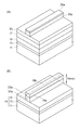
図4(A)を参照すると、化合物半導体領域10のIII―V化合物半導体膜15のエッチングが進み、エッチングされたIII―V化合物半導体膜15aが形成されている。このエッチングの進行中に、図3(B)に示された誘電体マスク17のエッジ18a、18bが消失している。つまり、エッチング中に、半導体領域11、13、15がエッチングにより加工されるだけでなく、誘電体マスク17の形状もエッチングの進行と共に変化する。このECR−RIE法では、図5(A)に示されるように、エッチングが進行するにつれて、マスクエッジ18a、18bから変形が進行する。この変形はスパッタ成分により引き起こされ、誘電体マスクの変形は、垂直方向のエッチング速度の8〜10倍の速度で進む。マスクの変形は、マスク上部のエッジからほぼ45度の角度方向に進み、これによりマスク上部および側面と約135度の角度を成す傾斜面18c、18dが形成される。
Referring to FIG. 4A, the etching of the III-V
一方、PE−CVD法によるSiN膜、および熱CVD法によるSiO2膜を厚くすると、割れが生じるので、厚膜のマスク膜が得られない。これらの膜から形成された誘電体マスク20を用いるエッチング方法でも、エッチング中に、半導体領域がエッチングにより加工されるだけでなく、マスクの形状もエッチングの進行と共に変化する。このエッチングでは、エッチングマスクとして厚さ0.3μm程度のSiN、SiO2等の絶縁膜を用いてRIE法を用いる。RIE法では、エッチングが進行するにつれて、マスク側面とマスク上面とからなるエッジ20a、20bから進行する(マスクエッジの変形)。図5(B)に示されるように、この変形はスパッタ成分により引き起こされマスク上部のエッジから45度の角度方向に進み、これによりマスク上部および側面と約135度の角度を成す傾斜面20c、20dが形成される。マスクの変形は、垂直方向のエッチング速度の8〜10倍の消失速度で進む。マスクの変形により側面が消失して傾斜面20e、20fが形成されると、エッチングの進行に伴いマスク幅WSが小さくなる(マスク幅の後退)。ドライエッチング中にマスク幅が縮小すると、メサ側面が裾を引くようになり、結果的にメサ幅はメサ上部に近づくにつれて狭くなる。このため、図6(B)に示されるように、エッチングされた半導体領域12の形状が、裾を引くリッジ形状になる。したがって、メサのエッチング角度を垂直に維持しながらドライエッチングを行うことができない。つまり、ドライエッチングにより直角に近い段差を形成することができない。
On the other hand, if the SiN film by the PE-CVD method and the SiO 2 film by the thermal CVD method are thickened, cracks occur, so that a thick mask film cannot be obtained. Even in the etching method using the
図4(B)を参照すると、化合物半導体領域10のIII―V化合物半導体膜15a、13、11のエッチングが完了し、エッチングされたIII―V化合物半導体領域15b、13b、11bが形成されている。一方、誘電体マスク17bはエッチングにより変形されて誘電体マスク17cになる。しかしながら、誘電体マスク17aは厚いので、エッチングの進行に伴いマスク幅が小さくなること(マスク幅の後退)はない。このため、半導体領域11b、13b、15bの形状が、ほぼ垂直にエッチングされたリッジ形状になる。これ故に、メサのエッチング角度を垂直に維持しながらドライエッチングを行うことができる。つまり、図6(A)に示されるように、エッチングの進行10a、10b、10cに伴い誘電体マスクの消失により傾斜面18c、18dから傾斜面18e、18fに変形していく。しかしながら、誘電体マスクのボトムの幅WBが実質的に変化しないので、ドライエッチングにより直角に近い段差を形成できる。既に説明したように、誘電体マスク17aは厚いので、エッチングの進行に伴いマスク幅が小さくなること(マスク幅の後退)はない。これ故に、メサのエッチング角度を垂直に維持しながらドライエッチングを行うことができる。つまり、ドライエッチングにより直角に近い段差を形成できる。
Referring to FIG. 4B, the etching of the III-V
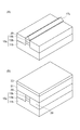
引き続いて、化合物半導体光デバイスを作製する方法を説明する。図7(A)は、化合物半導体光デバイスを作製する方法における埋め込み再成長工程を示す図面である。この工程においても、誘電体マスク17cは除去されずに残されている。誘電体マスク17cを用いてエッチングされた半導体領域10c上に電流ブロック領域29を成長する。誘電体マスク17cが設けられているメサ上には、化合物半導体が堆積されない。電流ブロック領域29は、例えば、鉄ドープInP、またはp型InP層およびn型InP層から成ることができる。電流ブロック領域29の成長は、例えば例えば有機金属気相成長炉を用いて行われる。電流ブロック領域29が形成された後に、誘電体マスク17cを除去する。
Subsequently, a method for producing a compound semiconductor optical device will be described. FIG. 7A is a drawing showing a buried regrowth step in a method of manufacturing a compound semiconductor optical device. Also in this step, the
図7(B)は、化合物半導体光デバイスを作製する方法における結晶成長工程を示す図面である。半導体領域10cのメサ上および電流ブロック領域29上にp型III―V化合物半導体膜31およびp型III―V化合物半導体コンタクト膜33を成長する。これらの工程の後に、アノード電極およびカソード電極を形成する。これにより、化合物半導体光デバイスを作製する方法の主要な工程が説明された。
FIG. 7B is a drawing showing a crystal growth step in a method for manufacturing a compound semiconductor optical device. A p-type III-V
埋め込み半導体レーザといった化合物半導体光デバイスの一例は
基板11:n型InP基板
n型III―V化合物半導体膜13:SiドープInP(n型クラッド)
活性領域15:InGaAsPからなる量子井戸構造
埋め込み領域29:FeドープInP(電流ブロック)
p型III―V化合物半導体膜31:ZnドープInP(p型クラッド)
p型III―V化合物半導体コンタクト膜33:ZnドープInGaAs
である。
An example of a compound semiconductor optical device such as a buried semiconductor laser is substrate 11: n-type InP substrate n-type III-V compound semiconductor film 13: Si-doped InP (n-type cladding)
Active region 15: buried region of
p-type III-V compound semiconductor film 31: Zn-doped InP (p-type cladding)
p-type III-V compound semiconductor contact film 33: Zn-doped InGaAs
It is.
本実施の形態に係る方法では、メサ形状の化合物半導体領域を形成するためのエッチング中に、誘電体マスク17は、該マスク17の上面のエッジ18a、18bから徐々に後退すると共に、この後退に伴い、図5(A)および図6(A)に示されるように、該マスクの側面の高さHMは徐々に小さくなる。ドライエッチングの終了のときに側面の高さHMが0以下にならないために、誘電体マスク17の厚みHは、
H≧h/3
の関係を満たすことが好ましい。この方法によれば、エッチング量が大きく高いメサ形状を作製することができる。例えば、SiO2からなる誘電体マスクの高さが約1μmであるとき、メサ側面の垂直性を保ちながらInP半導体を3.5μm程度の深さまでエッチングできる。誘電体マスクの厚みHは、エッチングにより作製されるべきメサの深さhの3倍程度にすることが好ましい。これにより、ドライエッチング時の横方向へのマスク減退が無くなるので、垂直なエッチング側面を有するメサを作製可能となる。また、横方向のマスク減退を防ぐことができるので、マスク幅に従ったエッチング形状の実現が可能となりエッチング幅の制御性が向上する。
In the method according to the present embodiment, during the etching for forming the mesa-shaped compound semiconductor region, the
H ≧ h / 3
It is preferable to satisfy the relationship. According to this method, a mesa shape with a large etching amount can be produced. For example, when the height of the dielectric mask made of SiO 2 is about 1 μm, the InP semiconductor can be etched to a depth of about 3.5 μm while maintaining the mesa side surface perpendicularity. The thickness H of the dielectric mask is preferably about three times the depth h of the mesa to be produced by etching. This eliminates the lateral mask reduction during dry etching, so that a mesa having a vertical etching side surface can be produced. Further, since the mask reduction in the horizontal direction can be prevented, an etching shape according to the mask width can be realized, and the controllability of the etching width is improved.
以上説明したように、本実施の形態に係るエッチング方法によれば、誘電体マスク17aのためのシリコン化合物が誘導結合プラズマ−化学的気相成長法で形成されるので、低応力のため1マイクロメートル以上の厚みを有する誘電体マスク17aを得ることができる。厚膜の誘電体マスク17aを用いて化合物半導体領域のドライエッチングを行うので、エッチング中にマスクエッジの消失が生じてもマスク幅が小さくなることはない。これ故に、所望のメサ形状の化合物半導体領域を形成できる。低応力で厚膜の誘電体マスク膜は、例えば、ICP放電を利用したプラズマCVD装置にTEOS原料を供給すると共に、加熱された基板上にバイアスを印加しながらシリコン酸化物を堆積することにより得られる。
As described above, according to the etching method according to the present embodiment, since the silicon compound for the
好適な実施の形態において本発明の原理を図示し説明してきたが、本発明は、そのような原理から逸脱することなく配置および詳細において変更され得ることは、当業者によって認識される。本実施の形態では、例えば、埋め込み型半導体レーザといった化合物半導体光デバイスを作製する方法を説明したけれども、本発明は、本実施の形態に開示された特定の構成に限定されるものではない。また、本実施の形態では、InP半導体を基板とするInP系埋め込み半導体レーザについて例示的に説明しているけれども、GaAs半導体を基板とするGaAs系埋め込み半導体レーザでもできる。したがって、特許請求の範囲およびその精神の範囲から来る全ての修正および変更に権利を請求する。 While the principles of the invention have been illustrated and described in the preferred embodiments, it will be appreciated by those skilled in the art that the invention can be modified in arrangement and detail without departing from such principles. In the present embodiment, for example, a method of manufacturing a compound semiconductor optical device such as a buried semiconductor laser has been described. However, the present invention is not limited to the specific configuration disclosed in the present embodiment. In the present embodiment, an InP embedded semiconductor laser using an InP semiconductor as a substrate has been described as an example, but a GaAs embedded semiconductor laser using a GaAs semiconductor as a substrate can also be used. We therefore claim all modifications and changes that come within the scope and spirit of the following claims.
11…基板、10…化合物半導体領域、10a、10b、10c…エッチングされた化合物半導体領域、11a…InP半導体表面、11b…III―V化合物半導体領域、13…活性領域、13b…III―V化合物半導体領域、15…III―V化合物半導体膜、15a…III―V化合物半導体膜、15b…III―V化合物半導体領域、17…誘電体マスク膜、17a…誘電体マスク、17b、17c…変形された誘電体マスク、HFILM…誘電体マスク膜厚み、HMASK…誘電体マスク厚み、19…第1のエッチングマスク材、21…多層構造、23…硬化されたレジスト膜、23a…硬化レジストマスク、25…シリコン化合物膜、25a…シリコン酸化物マスク、27…感光性レジスト膜、27a…レジストマスク、18a、18b…誘電体マスクエッジ、18c、18d…マスク傾斜面、18e、18f…マスク傾斜面、10…化合物半導体領域、29…電流ブロック領域、31…p型III―V化合物半導体膜、33…p型III―V化合物半導体コンタクト膜
DESCRIPTION OF
Claims (4)
基板上に、III−V化合物半導体から成る活性領域を含む化合物半導体領域を形成する工程と、
有機シラン系原料および酸素原料を含む成膜ガスを供給して、シリコン化合物からなる誘電体マスク膜を前記化合物半導体領域上に誘導結合プラズマ−化学的気相成長法で堆積する工程と、
前記誘電体マスク膜にパターンを形成して誘電体マスクを形成する工程と、
前記誘電体マスクを用いて、前記化合物半導体領域のドライエッチングを行って、メサ高さhが3.5μm以上のメサ形状の化合物半導体領域を形成する工程とを備え、
前記ドライエッチングは、バイアス電力を供給し炭化水素と水素の混合ガスを用いたRIEエッチングであり、
前記誘電体マスク膜は、前記メサ形状の化合物半導体領域を形成する工程後の該化合物半導体のメサ高さhとの間に前記誘電体マスクの厚みHがH≧h/3の関係を満しており、
前記エッチングにおいて、前記誘電体マスクの側面と上面によるマスクエッジの変形が前記エッチングのスパッタ成分により引き起こされ、該マスクエッジに傾斜面が形成され、
前記誘電体マスクが単層のシリコン化合物からなる、ことを特徴とする方法。 A method for producing a compound semiconductor optical device, comprising:
Forming a compound semiconductor region including an active region made of a III-V compound semiconductor on a substrate;
Depositing by chemical vapor deposition, - an organic silane material and the film forming gas containing an oxygen source are supplied inductively coupled plasma dielectric mask film made of a silicon compound to the compound semiconductor region
Forming a dielectric mask by forming a pattern on the dielectric mask film;
Using the dielectric mask to dry-etch the compound semiconductor region to form a mesa-shaped compound semiconductor region having a mesa height h of 3.5 μm or more,
The dry etching is RIE etching using a mixed gas of hydrocarbon and hydrogen by supplying bias power.
The dielectric mask film satisfies the relationship H ≧ h / 3 between the thickness H of the dielectric mask and the mesa height h of the compound semiconductor after the step of forming the mesa-shaped compound semiconductor region. And
In the etching, the deformation of the mask edge due to the side surface and the upper surface of the dielectric mask is caused by the sputter component of the etching, and an inclined surface is formed on the mask edge,
The dielectric mask is made of a single layer of silicon compound.
前記RIEエッチングはECR−RIEエッチングである、ことを特徴とする請求項1に記載された方法。 The bias power is 50 to 300 W,
The method according to claim 1, wherein the RIE etching is an ECR-RIE etching .
前記酸素原料は酸素分子を含み、
前記誘電体マスクの材料はシリコン酸化物からなる、請求項1または請求項2に記載された方法。 The organosilane material includes TEOS,
The oxygen source contains oxygen molecules;
The method according to claim 1, wherein the material of the dielectric mask is made of silicon oxide.
The hydrocarbon includes CH 4, the method according to any one of claims 1 to 3.
Priority Applications (1)
| Application Number | Priority Date | Filing Date | Title |
|---|---|---|---|
| JP2006027398A JP5028811B2 (en) | 2006-02-03 | 2006-02-03 | Method for fabricating compound semiconductor optical device |
Applications Claiming Priority (1)
| Application Number | Priority Date | Filing Date | Title |
|---|---|---|---|
| JP2006027398A JP5028811B2 (en) | 2006-02-03 | 2006-02-03 | Method for fabricating compound semiconductor optical device |
Publications (2)
| Publication Number | Publication Date |
|---|---|
| JP2007208134A JP2007208134A (en) | 2007-08-16 |
| JP5028811B2 true JP5028811B2 (en) | 2012-09-19 |
Family
ID=38487309
Family Applications (1)
| Application Number | Title | Priority Date | Filing Date |
|---|---|---|---|
| JP2006027398A Expired - Fee Related JP5028811B2 (en) | 2006-02-03 | 2006-02-03 | Method for fabricating compound semiconductor optical device |
Country Status (1)
| Country | Link |
|---|---|
| JP (1) | JP5028811B2 (en) |
Families Citing this family (1)
| Publication number | Priority date | Publication date | Assignee | Title |
|---|---|---|---|---|
| JP4985411B2 (en) * | 2008-01-08 | 2012-07-25 | 住友電気工業株式会社 | Method for fabricating a semiconductor optical device |
Family Cites Families (9)
| Publication number | Priority date | Publication date | Assignee | Title |
|---|---|---|---|---|
| US5431770A (en) * | 1993-10-13 | 1995-07-11 | At&T Corp. | Transistor gate formation |
| JPH07153595A (en) * | 1993-11-26 | 1995-06-16 | Canon Inc | Magnetic field inductively coupled plasma processing system |
| JPH08288272A (en) * | 1995-04-18 | 1996-11-01 | Sony Corp | Helicon wave plasma CVD method |
| JP3641866B2 (en) * | 1996-02-22 | 2005-04-27 | ソニー株式会社 | Manufacturing method of semiconductor device |
| JPH1197799A (en) * | 1997-09-22 | 1999-04-09 | Mitsubishi Electric Corp | Method for manufacturing semiconductor device |
| US6020091A (en) * | 1997-09-30 | 2000-02-01 | Siemens Aktiengesellschaft | Hard etch mask |
| JPH11135478A (en) * | 1997-10-27 | 1999-05-21 | Asahi Kasei Micro Syst Co Ltd | Manufacture of semiconductor device |
| JP3994362B2 (en) * | 1998-09-08 | 2007-10-17 | 富士通株式会社 | Method for manufacturing compound semiconductor device |
| JP2004281815A (en) * | 2003-03-17 | 2004-10-07 | Sumitomo Electric Ind Ltd | Etching method |
-
2006
- 2006-02-03 JP JP2006027398A patent/JP5028811B2/en not_active Expired - Fee Related
Also Published As
| Publication number | Publication date |
|---|---|
| JP2007208134A (en) | 2007-08-16 |
Similar Documents
| Publication | Publication Date | Title |
|---|---|---|
| JP3729210B2 (en) | Manufacturing method of semiconductor device | |
| CN108233175A (en) | A kind of production method for burying AlGaInAs Distributed Feedback Lasers | |
| US20120058582A1 (en) | Method for etching insulating film and method for manufacturing semiconductor optical device | |
| JP2010192888A (en) | Method to form semiconductor laser | |
| CN107437497A (en) | The forming method of semiconductor devices | |
| JP5028811B2 (en) | Method for fabricating compound semiconductor optical device | |
| US8357555B2 (en) | Method for producing semiconductor optical device | |
| JP5531610B2 (en) | Manufacturing method of semiconductor laser device | |
| JP4985411B2 (en) | Method for fabricating a semiconductor optical device | |
| JP5211728B2 (en) | Method for fabricating a semiconductor optical device | |
| JP4537549B2 (en) | Method for manufacturing compound semiconductor device | |
| JP5076713B2 (en) | Method for fabricating compound semiconductor optical device | |
| JP2010267674A (en) | Method for fabricating III-V compound semiconductor optical device | |
| JP2007184491A (en) | Distributed feedback laser diode | |
| JP2017011168A (en) | Method for fabricating semiconductor light receiving element | |
| JP4350227B2 (en) | Semiconductor crystal growth method | |
| JP2009129943A (en) | Nitride semiconductor device and manufacturing method thereof | |
| JP5239544B2 (en) | Method for fabricating a semiconductor optical device | |
| JP7359333B1 (en) | Optical semiconductor device and its manufacturing method | |
| JP5108687B2 (en) | Optical semiconductor device and manufacturing method thereof | |
| JP5239543B2 (en) | Method for fabricating a semiconductor optical device | |
| CN119481956A (en) | A method for preparing an EML laser and an air bridge | |
| CN115210976B (en) | Semiconductor device and method for manufacturing semiconductor device | |
| JP2009177076A (en) | Method for manufacturing a semiconductor device | |
| CN120676733A (en) | Preparation method of silicon-based germanium epitaxial window structure and semiconductor device |
Legal Events
| Date | Code | Title | Description |
|---|---|---|---|
| A621 | Written request for application examination |
Free format text: JAPANESE INTERMEDIATE CODE: A621 Effective date: 20081224 |
|
| A977 | Report on retrieval |
Free format text: JAPANESE INTERMEDIATE CODE: A971007 Effective date: 20090422 |
|
| A131 | Notification of reasons for refusal |
Free format text: JAPANESE INTERMEDIATE CODE: A131 Effective date: 20110719 |
|
| A521 | Written amendment |
Free format text: JAPANESE INTERMEDIATE CODE: A523 Effective date: 20110916 |
|
| TRDD | Decision of grant or rejection written | ||
| A01 | Written decision to grant a patent or to grant a registration (utility model) |
Free format text: JAPANESE INTERMEDIATE CODE: A01 Effective date: 20120529 |
|
| A01 | Written decision to grant a patent or to grant a registration (utility model) |
Free format text: JAPANESE INTERMEDIATE CODE: A01 |
|
| A61 | First payment of annual fees (during grant procedure) |
Free format text: JAPANESE INTERMEDIATE CODE: A61 Effective date: 20120611 |
|
| R150 | Certificate of patent or registration of utility model |
Free format text: JAPANESE INTERMEDIATE CODE: R150 |
|
| FPAY | Renewal fee payment (event date is renewal date of database) |
Free format text: PAYMENT UNTIL: 20150706 Year of fee payment: 3 |
|
| R250 | Receipt of annual fees |
Free format text: JAPANESE INTERMEDIATE CODE: R250 |
|
| LAPS | Cancellation because of no payment of annual fees |