JP5009500B2 - Rfパワーデバイス及びrfパワートランジスタデバイスにおける直線性を改善する方法 - Google Patents
Rfパワーデバイス及びrfパワートランジスタデバイスにおける直線性を改善する方法 Download PDFInfo
- Publication number
- JP5009500B2 JP5009500B2 JP2004541592A JP2004541592A JP5009500B2 JP 5009500 B2 JP5009500 B2 JP 5009500B2 JP 2004541592 A JP2004541592 A JP 2004541592A JP 2004541592 A JP2004541592 A JP 2004541592A JP 5009500 B2 JP5009500 B2 JP 5009500B2
- Authority
- JP
- Japan
- Prior art keywords
- transistor
- coupled
- package
- matching circuit
- lead
- Prior art date
- Legal status (The legal status is an assumption and is not a legal conclusion. Google has not performed a legal analysis and makes no representation as to the accuracy of the status listed.)
- Expired - Lifetime
Links
- 238000000034 method Methods 0.000 title claims description 10
- 239000003990 capacitor Substances 0.000 claims description 42
- 230000001939 inductive effect Effects 0.000 claims description 10
- 230000008878 coupling Effects 0.000 claims description 5
- 238000010168 coupling process Methods 0.000 claims description 5
- 238000005859 coupling reaction Methods 0.000 claims description 5
- 238000010586 diagram Methods 0.000 description 17
- 238000013459 approach Methods 0.000 description 3
- 238000004891 communication Methods 0.000 description 3
- 230000003071 parasitic effect Effects 0.000 description 3
- 230000003321 amplification Effects 0.000 description 2
- 238000003199 nucleic acid amplification method Methods 0.000 description 2
- 230000005540 biological transmission Effects 0.000 description 1
- 239000004020 conductor Substances 0.000 description 1
- 230000000593 degrading effect Effects 0.000 description 1
- 238000013461 design Methods 0.000 description 1
- 230000001627 detrimental effect Effects 0.000 description 1
- 230000009977 dual effect Effects 0.000 description 1
- 238000005516 engineering process Methods 0.000 description 1
- 230000006872 improvement Effects 0.000 description 1
- 239000000463 material Substances 0.000 description 1
- 238000012986 modification Methods 0.000 description 1
- 230000004048 modification Effects 0.000 description 1
- 238000000926 separation method Methods 0.000 description 1
- 229910052710 silicon Inorganic materials 0.000 description 1
- 239000010703 silicon Substances 0.000 description 1
- 230000009466 transformation Effects 0.000 description 1
Images


Classifications
-
- H—ELECTRICITY
- H03—ELECTRONIC CIRCUITRY
- H03F—AMPLIFIERS
- H03F3/00—Amplifiers with only discharge tubes or only semiconductor devices as amplifying elements
- H03F3/189—High frequency amplifiers, e.g. radio frequency amplifiers
- H03F3/19—High frequency amplifiers, e.g. radio frequency amplifiers with semiconductor devices only
- H03F3/195—High frequency amplifiers, e.g. radio frequency amplifiers with semiconductor devices only in integrated circuits
-
- H—ELECTRICITY
- H01—ELECTRIC ELEMENTS
- H01L—SEMICONDUCTOR DEVICES NOT COVERED BY CLASS H10
- H01L23/00—Details of semiconductor or other solid state devices
- H01L23/58—Structural electrical arrangements for semiconductor devices not otherwise provided for, e.g. in combination with batteries
- H01L23/64—Impedance arrangements
- H01L23/66—High-frequency adaptations
-
- H—ELECTRICITY
- H03—ELECTRONIC CIRCUITRY
- H03F—AMPLIFIERS
- H03F1/00—Details of amplifiers with only discharge tubes, only semiconductor devices or only unspecified devices as amplifying elements
- H03F1/56—Modifications of input or output impedances, not otherwise provided for
-
- H—ELECTRICITY
- H01—ELECTRIC ELEMENTS
- H01L—SEMICONDUCTOR DEVICES NOT COVERED BY CLASS H10
- H01L2223/00—Details relating to semiconductor or other solid state devices covered by the group H01L23/00
- H01L2223/58—Structural electrical arrangements for semiconductor devices not otherwise provided for
- H01L2223/64—Impedance arrangements
- H01L2223/66—High-frequency adaptations
- H01L2223/6644—Packaging aspects of high-frequency amplifiers
- H01L2223/665—Bias feed arrangements
-
- H—ELECTRICITY
- H01—ELECTRIC ELEMENTS
- H01L—SEMICONDUCTOR DEVICES NOT COVERED BY CLASS H10
- H01L2224/00—Indexing scheme for arrangements for connecting or disconnecting semiconductor or solid-state bodies and methods related thereto as covered by H01L24/00
- H01L2224/01—Means for bonding being attached to, or being formed on, the surface to be connected, e.g. chip-to-package, die-attach, "first-level" interconnects; Manufacturing methods related thereto
- H01L2224/42—Wire connectors; Manufacturing methods related thereto
- H01L2224/47—Structure, shape, material or disposition of the wire connectors after the connecting process
- H01L2224/48—Structure, shape, material or disposition of the wire connectors after the connecting process of an individual wire connector
- H01L2224/4805—Shape
- H01L2224/4809—Loop shape
- H01L2224/48091—Arched
-
- H—ELECTRICITY
- H01—ELECTRIC ELEMENTS
- H01L—SEMICONDUCTOR DEVICES NOT COVERED BY CLASS H10
- H01L2924/00—Indexing scheme for arrangements or methods for connecting or disconnecting semiconductor or solid-state bodies as covered by H01L24/00
- H01L2924/10—Details of semiconductor or other solid state devices to be connected
- H01L2924/11—Device type
- H01L2924/13—Discrete devices, e.g. 3 terminal devices
- H01L2924/1304—Transistor
- H01L2924/1305—Bipolar Junction Transistor [BJT]
-
- H—ELECTRICITY
- H01—ELECTRIC ELEMENTS
- H01L—SEMICONDUCTOR DEVICES NOT COVERED BY CLASS H10
- H01L2924/00—Indexing scheme for arrangements or methods for connecting or disconnecting semiconductor or solid-state bodies as covered by H01L24/00
- H01L2924/30—Technical effects
- H01L2924/301—Electrical effects
- H01L2924/30107—Inductance
-
- H—ELECTRICITY
- H01—ELECTRIC ELEMENTS
- H01L—SEMICONDUCTOR DEVICES NOT COVERED BY CLASS H10
- H01L2924/00—Indexing scheme for arrangements or methods for connecting or disconnecting semiconductor or solid-state bodies as covered by H01L24/00
- H01L2924/30—Technical effects
- H01L2924/301—Electrical effects
- H01L2924/3011—Impedance
Description
Claims (18)
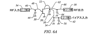
- a)少なくとも一つのトランジスタと、
b)前記トランジスタに結合されたRF信号入力リード線と、
c)前記トランジスタに結合された接地端子と、
d)前記トランジスタに結合されたRF信号出力リード線と、
e)前記RF信号出力リード線に結合された出力マッチング回路であって前記トランジスタが該出力マッチング回路を介して前記RF信号出力リード線に結合された出力マッチング回路、および該出力マッチング回路を介して前記RF信号出力リード線に結合されたRF及びビデオバイパス回路と、
f)要素a)及びe)を収容するパッケージで、要素b)、c)、及びd)が前記パッケージから延出された状態となるパッケージと、
g)前記RF及びビデオバイパス回路に結合され、前記パッケージから延出したバイアスリード線と、
を備えた、パッケージに収納されたRFパワーデバイス。 - a)少なくとも一つのトランジスタと、
b)前記トランジスタに結合されたRF信号入力リード線と、
c)前記トランジスタに結合された接地端子と、
d)前記トランジスタに結合されたRF信号出力リード線と、
e)前記RF信号出力リード線に結合された出力マッチング回路であって前記トランジスタが該出力マッチング回路を介して前記RF信号出力リード線に結合された出力マッチング回路、および該出力マッチング回路を介して前記RF信号出力リード線に結合されたRF及びビデオバイパス回路と、
f)要素a)及びe)を収容するパッケージで、要素b)、c)、及びd)が前記パッケージから延出された状態となるパッケージと、
g)前記RF及びビデオバイパス回路を介して前記トランジスタにDCバイアス電圧を印加するためのバイアスリード線とを備え、前記RF信号出力リード線と前記バイアスリード線は兼用されているパッケージに収納されたRFパワーデバイス。 - 前記RF及びビデオバイパス回路は、少なくとも一つの個別キャパシタと、前記個別キャパシタを前記トランジスタに結合するワイヤボンディングとを備え、前記ワイヤボンディングは、前記RFバイパス回路においてインダクタンスを提供する請求項1記載のパッケージに収納されたRFパワーデバイス。
- 前記出力マッチング回路は、接地に直列で接続された誘導素子及び容量素子を、ワイヤボンディングによって前記容量素子と並列に接続された少なくとも一つの個別キャパシタと共に含む請求項3記載のパッケージに収納されたRFパワーデバイス。
- 前記少なくとも一つの個別キャパシタは、複数の個別多層キャパシタを備える請求項4記載のパッケージに収納されたRFパワーデバイス。
- 前記RF及びビデオバイパス回路は、少なくとも一つの個別キャパシタと、前記個別キャパシタを前記トランジスタに結合するワイヤボンディングとを備え、前記ワイヤボンディングは、前記RFバイパス回路においてインダクタンスを備える請求項1記載のパッケージに収納されたRFパワーデバイス。
- 前記出力マッチング回路は、接地に直列で接続された誘導素子及び容量素子を、ワイヤボンディングによって前記容量素子と並列に接続された少なくとも一つの個別キャパシタと共に含む請求項6記載のパッケージに収納されたRFパワーデバイス。
- 前記少なくとも一つの個別キャパシタは、複数のキャパシタを備える請求項7記載のパッケージに収納されたRFパワーデバイス。
- 前記少なくとも一つのトランジスタは、FETを備える請求項1記載のパッケージに収納されたRFパワーデバイス。
- 前記少なくとも一つのトランジスタは、バイポーラトランジスタを備える請求項1記載のパッケージに収納されたRFパワーデバイス。
- 前記少なくとも一つのトランジスタは、複数のトランジスタを備える請求項1記載のパッケージに収納されたRFパワーデバイス。
- a)少なくとも一つのRFパワートランジスタをハウジング内に提供するステップと、
b)前記ハウジングから延出し、前記トランジスタに電気的に結合されたRF信号入力リード線及びRF信号出力リード線を提供するステップと、
c)前記RF信号出力リード線に結合された出力マッチング回路であって前記トランジスタが該出力マッチング回路を介して前記RF信号出力リード線に結合された出力マッチング回路を前記ハウジング内に提供するステップと、
d)前記出力マッチング回路を介して前記RF信号出力リード線に接続され、DC電力を前記トランジスタに供給する時、RF及びビデオ電流がDC電源へ流れるのを防止するRF及びビデオバイパス回路であって前記トランジスタが該出力マッチング回路を介して結合されたRF及びビデオバイパス回路を前記ハウジング内に提供するステップと、
e)前記ハウジングから延出し、前記トランジスタ、前記RFおよびビデオバイパス回路に接続されて前記DC電源を供給するバイアスリード線を提供するステップと
を備え、前記RF信号出力リード線と前記バイアスリード線は兼用されている広帯域RFパワートランジスタデバイスにおける直線性を改善する方法。 - ステップd)の前記RF及びビデオバイパス回路は、少なくとも一つの個別キャパシタと、前記個別キャパシタを前記トランジスタに結合するワイヤボンディングとを備え、前記ワイヤボンディングは、前記RFバイパス回路においてインダクタンスを提供する請求項12記載の方法。
- ステップc)の前記出力マッチング回路は、接地に直列で接続された誘導素子及び容量素子を、ワイヤボンディングによって前記容量素子と並列に接続された少なくとも一つの個別キャパシタと共に含む請求項13記載の方法。
- ステップd)の前記少なくとも一つの個別キャパシタは、複数のキャパシタを備える請求項14記載の方法。
- ステップd)の前記RFバイパス回路は、少なくとも一つの個別キャパシタと、前記個別キャパシタを前記トランジスタに結合するワイヤボンディングとを備え、前記ワイヤボンディングは、前記RFバイパス回路においてインダクタンスを提供する請求項12記載の方法。
- ステップc)の前記出力マッチング回路は、接地に直列で接続された誘導素子及び容量素子を、ワイヤボンディングによって前記容量素子と並列に接続された少なくとも一つの個別キャパシタと共に含む請求項16記載の方法。
- ステップd)の前記少なくとも一つの個別キャパシタは、複数の個別キャパシタを備える請求項17記載の方法。
Applications Claiming Priority (3)
| Application Number | Priority Date | Filing Date | Title |
|---|---|---|---|
| US10/262,217 US6822321B2 (en) | 2002-09-30 | 2002-09-30 | Packaged RF power transistor having RF bypassing/output matching network |
| US10/262,217 | 2002-09-30 | ||
| PCT/US2003/029719 WO2004032188A2 (en) | 2002-09-30 | 2003-09-17 | Packaged rf power transistor having rf bypassing/output matching network |
Publications (3)
| Publication Number | Publication Date |
|---|---|
| JP2006501678A JP2006501678A (ja) | 2006-01-12 |
| JP2006501678A5 JP2006501678A5 (ja) | 2006-11-02 |
| JP5009500B2 true JP5009500B2 (ja) | 2012-08-22 |
Family
ID=32030167
Family Applications (1)
| Application Number | Title | Priority Date | Filing Date |
|---|---|---|---|
| JP2004541592A Expired - Lifetime JP5009500B2 (ja) | 2002-09-30 | 2003-09-17 | Rfパワーデバイス及びrfパワートランジスタデバイスにおける直線性を改善する方法 |
Country Status (7)
| Country | Link |
|---|---|
| US (1) | US6822321B2 (ja) |
| EP (1) | EP1547394B1 (ja) |
| JP (1) | JP5009500B2 (ja) |
| CN (1) | CN1701613B (ja) |
| AU (1) | AU2003275086A1 (ja) |
| TW (1) | TWI318455B (ja) |
| WO (1) | WO2004032188A2 (ja) |
Families Citing this family (43)
| Publication number | Priority date | Publication date | Assignee | Title |
|---|---|---|---|---|
| US7109589B2 (en) * | 2004-08-26 | 2006-09-19 | Agere Systems Inc. | Integrated circuit with substantially perpendicular wire bonds |
| US7268627B2 (en) * | 2004-11-03 | 2007-09-11 | Theta Microelectronics, Inc. | Pre-matching of distributed and push-pull power transistors |
| US20060138650A1 (en) * | 2004-12-28 | 2006-06-29 | Freescale Semiconductor, Inc. | Integrated circuit packaging device and method for matching impedance |
| US7193473B2 (en) * | 2005-03-24 | 2007-03-20 | Cree, Inc. | High power Doherty amplifier using multi-stage modules |
| US7564303B2 (en) * | 2005-07-26 | 2009-07-21 | Infineon Technologies Ag | Semiconductor power device and RF signal amplifier |
| US7372334B2 (en) | 2005-07-26 | 2008-05-13 | Infineon Technologies Ag | Output match transistor |
| US7378920B2 (en) * | 2006-02-14 | 2008-05-27 | Freescale Semiconductor, Inc. | Methods and apparatus for a high-frequency output match circuit |
| WO2007122586A2 (en) * | 2006-04-26 | 2007-11-01 | Nxp B.V. | A high power integrated rf amplifier |
| US20080231373A1 (en) * | 2007-03-20 | 2008-09-25 | Hafizur Rahman | Output Circuit |
| US8076994B2 (en) * | 2007-06-22 | 2011-12-13 | Cree, Inc. | RF power transistor packages with internal harmonic frequency reduction and methods of forming RF power transistor packages with internal harmonic frequency reduction |
| US8592966B2 (en) * | 2007-06-22 | 2013-11-26 | Cree, Inc. | RF transistor packages with internal stability network including intra-capacitor resistors and methods of forming RF transistor packages with internal stability networks including intra-capacitor resistors |
| US8330265B2 (en) * | 2007-06-22 | 2012-12-11 | Cree, Inc. | RF transistor packages with internal stability network and methods of forming RF transistor packages with internal stability networks |
| JP5030228B2 (ja) * | 2007-11-30 | 2012-09-19 | 矢崎総業株式会社 | 電気接続箱 |
| US9041470B2 (en) * | 2008-04-22 | 2015-05-26 | Freescale Semiconductor, Inc. | Wireless communication unit and semiconductor device having a power amplifier therefor |
| US7948312B2 (en) * | 2009-05-13 | 2011-05-24 | Qualcomm, Incorporated | Multi-bit class-D power amplifier system |
| US8536950B2 (en) * | 2009-08-03 | 2013-09-17 | Qualcomm Incorporated | Multi-stage impedance matching |
| US8102205B2 (en) | 2009-08-04 | 2012-01-24 | Qualcomm, Incorporated | Amplifier module with multiple operating modes |
| US8659359B2 (en) | 2010-04-22 | 2014-02-25 | Freescale Semiconductor, Inc. | RF power transistor circuit |
| EP2388815A1 (en) * | 2010-05-10 | 2011-11-23 | Nxp B.V. | A transistor package |
| USD668658S1 (en) * | 2011-11-15 | 2012-10-09 | Connectblue Ab | Module |
| USD692896S1 (en) * | 2011-11-15 | 2013-11-05 | Connectblue Ab | Module |
| USD680545S1 (en) * | 2011-11-15 | 2013-04-23 | Connectblue Ab | Module |
| USD689053S1 (en) * | 2011-11-15 | 2013-09-03 | Connectblue Ab | Module |
| USD668659S1 (en) * | 2011-11-15 | 2012-10-09 | Connectblue Ab | Module |
| USD680119S1 (en) * | 2011-11-15 | 2013-04-16 | Connectblue Ab | Module |
| US9281283B2 (en) | 2012-09-12 | 2016-03-08 | Freescale Semiconductor, Inc. | Semiconductor devices with impedance matching-circuits |
| EP2802075B1 (en) | 2013-05-07 | 2017-02-15 | Ampleon Netherlands B.V. | Dual-band semiconductor RF amplifier device |
| EP2830089B1 (en) * | 2013-07-25 | 2017-07-12 | Ampleon Netherlands B.V. | RF power device |
| US9979388B2 (en) | 2013-11-07 | 2018-05-22 | Nxp Usa, Inc. | Adjustable losses of bond wire arrangement |
| CN105308858B (zh) * | 2014-03-21 | 2019-04-05 | 华为技术有限公司 | 一种功率放大电路及发射机 |
| US9641163B2 (en) | 2014-05-28 | 2017-05-02 | Cree, Inc. | Bandwidth limiting methods for GaN power transistors |
| US9472480B2 (en) | 2014-05-28 | 2016-10-18 | Cree, Inc. | Over-mold packaging for wide band-gap semiconductor devices |
| US9515011B2 (en) | 2014-05-28 | 2016-12-06 | Cree, Inc. | Over-mold plastic packaged wide band-gap power transistors and MMICS |
| US9438184B2 (en) | 2014-06-27 | 2016-09-06 | Freescale Semiconductor, Inc. | Integrated passive device assemblies for RF amplifiers, and methods of manufacture thereof |
| CN105322895B (zh) * | 2015-05-06 | 2018-11-09 | 苏州能讯高能半导体有限公司 | 一种偏置自适应内匹配功放管及基于该功放管的功放模块 |
| US10432152B2 (en) | 2015-05-22 | 2019-10-01 | Nxp Usa, Inc. | RF amplifier output circuit device with integrated current path, and methods of manufacture thereof |
| US9692363B2 (en) * | 2015-10-21 | 2017-06-27 | Nxp Usa, Inc. | RF power transistors with video bandwidth circuits, and methods of manufacture thereof |
| US9571044B1 (en) | 2015-10-21 | 2017-02-14 | Nxp Usa, Inc. | RF power transistors with impedance matching circuits, and methods of manufacture thereof |
| CN106206524B (zh) * | 2016-07-07 | 2019-01-22 | 昆山华太电子技术有限公司 | 一种封装管壳体 |
| US10270402B1 (en) * | 2017-11-30 | 2019-04-23 | Nxp Usa, Inc. | Broadband input matching and video bandwidth circuits for power amplifiers |
| US10673386B2 (en) * | 2017-12-05 | 2020-06-02 | Nxp Usa, Inc. | Wideband power amplifiers with harmonic traps |
| CN111510085B (zh) * | 2020-05-12 | 2023-06-23 | 苏州远创达科技有限公司 | 一种功率放大器的输出电路 |
| US20230197587A1 (en) * | 2021-12-17 | 2023-06-22 | Wolfspeed, Inc. | Ipd components having sic substrates and devices and processes implementing the same |
Family Cites Families (14)
| Publication number | Priority date | Publication date | Assignee | Title |
|---|---|---|---|---|
| JPS58131775A (ja) * | 1982-01-29 | 1983-08-05 | Fujitsu Ltd | 電界効果半導体装置 |
| JPH0233963A (ja) * | 1988-07-23 | 1990-02-05 | Nec Corp | 高周波トランジスタ |
| JPH03283901A (ja) * | 1990-03-30 | 1991-12-13 | Nec Corp | ハイブリット型マイクロ波集積回路 |
| US5272450A (en) | 1991-06-20 | 1993-12-21 | Microwave Modules & Devices, Inc. | DC feed network for wideband RF power amplifier |
| US5309014A (en) * | 1992-04-02 | 1994-05-03 | Motorola Inc. | Transistor package |
| US5752182A (en) * | 1994-05-09 | 1998-05-12 | Matsushita Electric Industrial Co., Ltd. | Hybrid IC |
| JPH08222657A (ja) * | 1995-02-17 | 1996-08-30 | Hitachi Ltd | 半導体集積回路装置 |
| US6675383B1 (en) * | 1997-01-22 | 2004-01-06 | Nielsen Media Research, Inc. | Source detection apparatus and method for audience measurement |
| US6081160A (en) * | 1998-05-20 | 2000-06-27 | Powerwave Technologies, Inc. | Method and apparatus for increasing the bandwidth, and reducing the size, of the DC feed network for wideband RF amplifiers using selective placement of high dielectric constant material |
| US6791419B1 (en) * | 1998-12-02 | 2004-09-14 | Ericsson, Inc. | Constant gain, constant phase RF power block |
| JP4163818B2 (ja) * | 1999-07-07 | 2008-10-08 | 三菱電機株式会社 | 内部整合型トランジスタ |
| US20020050851A1 (en) * | 1999-12-22 | 2002-05-02 | Grundlingh Johan M. | Method and apparatus for biasing radio frequency power transistors |
| JP4256575B2 (ja) * | 2000-08-15 | 2009-04-22 | パナソニック株式会社 | バイアホールを備えた高周波受動回路および高周波増幅器 |
| JP2002176368A (ja) * | 2001-07-11 | 2002-06-21 | Nec Corp | 送信出力増幅器のバイアス電流最適化制御が可能な送信電力制御装置 |
-
2002
- 2002-09-30 US US10/262,217 patent/US6822321B2/en not_active Expired - Lifetime
-
2003
- 2003-09-17 WO PCT/US2003/029719 patent/WO2004032188A2/en active Application Filing
- 2003-09-17 CN CN038253658A patent/CN1701613B/zh not_active Expired - Lifetime
- 2003-09-17 AU AU2003275086A patent/AU2003275086A1/en not_active Abandoned
- 2003-09-17 JP JP2004541592A patent/JP5009500B2/ja not_active Expired - Lifetime
- 2003-09-17 EP EP03759357.1A patent/EP1547394B1/en not_active Expired - Lifetime
- 2003-09-23 TW TW092126215A patent/TWI318455B/zh not_active IP Right Cessation
Also Published As
| Publication number | Publication date |
|---|---|
| WO2004032188A3 (en) | 2004-06-17 |
| CN1701613B (zh) | 2010-10-13 |
| AU2003275086A1 (en) | 2004-04-23 |
| WO2004032188A2 (en) | 2004-04-15 |
| EP1547394A2 (en) | 2005-06-29 |
| AU2003275086A8 (en) | 2004-04-23 |
| EP1547394A4 (en) | 2006-09-20 |
| CN1701613A (zh) | 2005-11-23 |
| JP2006501678A (ja) | 2006-01-12 |
| TWI318455B (en) | 2009-12-11 |
| US6822321B2 (en) | 2004-11-23 |
| EP1547394B1 (en) | 2016-07-27 |
| TW200408128A (en) | 2004-05-16 |
| US20040061214A1 (en) | 2004-04-01 |
Similar Documents
| Publication | Publication Date | Title |
|---|---|---|
| JP5009500B2 (ja) | Rfパワーデバイス及びrfパワートランジスタデバイスにおける直線性を改善する方法 | |
| EP2458730B1 (en) | Radiofrequency amplifier | |
| US6046641A (en) | Parallel HV MOSFET high power stable amplifier | |
| US7508267B1 (en) | GaN based digital controlled broadband MMIC power amplifier | |
| JP3663397B2 (ja) | 高周波電力増幅器 | |
| US9531328B2 (en) | Amplifiers with a short phase path, packaged RF devices for use therein, and methods of manufacture thereof | |
| US9685915B2 (en) | Amplification stage and wideband power amplifier | |
| US7119623B2 (en) | Output circuit for a semiconductor amplifier element | |
| JP2005318093A (ja) | 高周波スイッチ回路 | |
| US9979360B1 (en) | Multi baseband termination components for RF power amplifier with enhanced video bandwidth | |
| WO2009060264A1 (en) | Integrated circuit having harmonic termination circuitry | |
| US9450545B2 (en) | Dual-band semiconductor RF amplifier device | |
| EP3694102B1 (en) | Amplifiers and amplifier modules having stub circuits | |
| US8299857B2 (en) | RF power amplifier including broadband input matching network | |
| JP2002171138A (ja) | マイクロ波電力増幅器 | |
| CN110829988A (zh) | 具有宽带阻抗匹配的放大器和其制造方法 | |
| US6731174B2 (en) | Radio frequency power amplifier device | |
| CN110417357B (zh) | 一种紧凑型集成多赫蒂放大器 | |
| US11677358B2 (en) | Power amplifier circuit | |
| CN110417355B (zh) | 一种集成高阻线多赫蒂放大器 | |
| JP2008236354A (ja) | 増幅器 | |
| US20240162862A1 (en) | Amplifier device with low frequency resonance decoupling circuitry | |
| JP2006025405A (ja) | 接続回路装置 | |
| KR101563212B1 (ko) | 고출력 반도체 소자 패키지 | |
| KR101601829B1 (ko) | 고출력 반도체 소자 패키지 |
Legal Events
| Date | Code | Title | Description |
|---|---|---|---|
| A521 | Request for written amendment filed |
Free format text: JAPANESE INTERMEDIATE CODE: A523 Effective date: 20060914 |
|
| A621 | Written request for application examination |
Free format text: JAPANESE INTERMEDIATE CODE: A621 Effective date: 20060914 |
|
| A977 | Report on retrieval |
Free format text: JAPANESE INTERMEDIATE CODE: A971007 Effective date: 20090828 |
|
| A131 | Notification of reasons for refusal |
Free format text: JAPANESE INTERMEDIATE CODE: A131 Effective date: 20090908 |
|
| A521 | Request for written amendment filed |
Free format text: JAPANESE INTERMEDIATE CODE: A523 Effective date: 20091208 |
|
| A131 | Notification of reasons for refusal |
Free format text: JAPANESE INTERMEDIATE CODE: A131 Effective date: 20100824 |
|
| A601 | Written request for extension of time |
Free format text: JAPANESE INTERMEDIATE CODE: A601 Effective date: 20101112 |
|
| A602 | Written permission of extension of time |
Free format text: JAPANESE INTERMEDIATE CODE: A602 Effective date: 20101119 |
|
| A521 | Request for written amendment filed |
Free format text: JAPANESE INTERMEDIATE CODE: A523 Effective date: 20110224 |
|
| A521 | Request for written amendment filed |
Free format text: JAPANESE INTERMEDIATE CODE: A523 Effective date: 20110526 |
|
| A711 | Notification of change in applicant |
Free format text: JAPANESE INTERMEDIATE CODE: A712 Effective date: 20110526 |
|
| A521 | Request for written amendment filed |
Free format text: JAPANESE INTERMEDIATE CODE: A821 Effective date: 20110526 |
|
| A521 | Request for written amendment filed |
Free format text: JAPANESE INTERMEDIATE CODE: A523 Effective date: 20110526 |
|
| A131 | Notification of reasons for refusal |
Free format text: JAPANESE INTERMEDIATE CODE: A131 Effective date: 20111209 |
|
| A601 | Written request for extension of time |
Free format text: JAPANESE INTERMEDIATE CODE: A601 Effective date: 20120309 |
|
| A602 | Written permission of extension of time |
Free format text: JAPANESE INTERMEDIATE CODE: A602 Effective date: 20120316 |
|
| A521 | Request for written amendment filed |
Free format text: JAPANESE INTERMEDIATE CODE: A523 Effective date: 20120409 |
|
| TRDD | Decision of grant or rejection written | ||
| A01 | Written decision to grant a patent or to grant a registration (utility model) |
Free format text: JAPANESE INTERMEDIATE CODE: A01 Effective date: 20120515 |
|
| A01 | Written decision to grant a patent or to grant a registration (utility model) |
Free format text: JAPANESE INTERMEDIATE CODE: A01 |
|
| A61 | First payment of annual fees (during grant procedure) |
Free format text: JAPANESE INTERMEDIATE CODE: A61 Effective date: 20120531 |
|
| R150 | Certificate of patent or registration of utility model |
Free format text: JAPANESE INTERMEDIATE CODE: R150 Ref document number: 5009500 Country of ref document: JP Free format text: JAPANESE INTERMEDIATE CODE: R150 |
|
| FPAY | Renewal fee payment (event date is renewal date of database) |
Free format text: PAYMENT UNTIL: 20150608 Year of fee payment: 3 |
|
| R250 | Receipt of annual fees |
Free format text: JAPANESE INTERMEDIATE CODE: R250 |
|
| R250 | Receipt of annual fees |
Free format text: JAPANESE INTERMEDIATE CODE: R250 |
|
| R250 | Receipt of annual fees |
Free format text: JAPANESE INTERMEDIATE CODE: R250 |
|
| R250 | Receipt of annual fees |
Free format text: JAPANESE INTERMEDIATE CODE: R250 |
|
| R250 | Receipt of annual fees |
Free format text: JAPANESE INTERMEDIATE CODE: R250 |
|
| R250 | Receipt of annual fees |
Free format text: JAPANESE INTERMEDIATE CODE: R250 |
|
| R250 | Receipt of annual fees |
Free format text: JAPANESE INTERMEDIATE CODE: R250 |
|
| R250 | Receipt of annual fees |
Free format text: JAPANESE INTERMEDIATE CODE: R250 |
|
| R250 | Receipt of annual fees |
Free format text: JAPANESE INTERMEDIATE CODE: R250 |
|
| EXPY | Cancellation because of completion of term |