US5309014A - Transistor package - Google Patents
Transistor package Download PDFInfo
- Publication number
- US5309014A US5309014A US07/862,106 US86210692A US5309014A US 5309014 A US5309014 A US 5309014A US 86210692 A US86210692 A US 86210692A US 5309014 A US5309014 A US 5309014A
- Authority
- US
- United States
- Prior art keywords
- metalized
- center portion
- lead
- substrate
- transistor
- Prior art date
- Legal status (The legal status is an assumption and is not a legal conclusion. Google has not performed a legal analysis and makes no representation as to the accuracy of the status listed.)
- Expired - Lifetime
Links
Images

Classifications
-
- H—ELECTRICITY
- H01—ELECTRIC ELEMENTS
- H01L—SEMICONDUCTOR DEVICES NOT COVERED BY CLASS H10
- H01L23/00—Details of semiconductor or other solid state devices
- H01L23/58—Structural electrical arrangements for semiconductor devices not otherwise provided for, e.g. in combination with batteries
- H01L23/64—Impedance arrangements
- H01L23/66—High-frequency adaptations
-
- H—ELECTRICITY
- H01—ELECTRIC ELEMENTS
- H01L—SEMICONDUCTOR DEVICES NOT COVERED BY CLASS H10
- H01L23/00—Details of semiconductor or other solid state devices
- H01L23/12—Mountings, e.g. non-detachable insulating substrates
- H01L23/13—Mountings, e.g. non-detachable insulating substrates characterised by the shape
-
- H—ELECTRICITY
- H01—ELECTRIC ELEMENTS
- H01L—SEMICONDUCTOR DEVICES NOT COVERED BY CLASS H10
- H01L24/00—Arrangements for connecting or disconnecting semiconductor or solid-state bodies; Methods or apparatus related thereto
- H01L24/01—Means for bonding being attached to, or being formed on, the surface to be connected, e.g. chip-to-package, die-attach, "first-level" interconnects; Manufacturing methods related thereto
- H01L24/42—Wire connectors; Manufacturing methods related thereto
- H01L24/47—Structure, shape, material or disposition of the wire connectors after the connecting process
- H01L24/49—Structure, shape, material or disposition of the wire connectors after the connecting process of a plurality of wire connectors
-
- H—ELECTRICITY
- H01—ELECTRIC ELEMENTS
- H01L—SEMICONDUCTOR DEVICES NOT COVERED BY CLASS H10
- H01L2223/00—Details relating to semiconductor or other solid state devices covered by the group H01L23/00
- H01L2223/58—Structural electrical arrangements for semiconductor devices not otherwise provided for
- H01L2223/64—Impedance arrangements
- H01L2223/66—High-frequency adaptations
- H01L2223/6644—Packaging aspects of high-frequency amplifiers
-
- H—ELECTRICITY
- H01—ELECTRIC ELEMENTS
- H01L—SEMICONDUCTOR DEVICES NOT COVERED BY CLASS H10
- H01L2224/00—Indexing scheme for arrangements for connecting or disconnecting semiconductor or solid-state bodies and methods related thereto as covered by H01L24/00
- H01L2224/01—Means for bonding being attached to, or being formed on, the surface to be connected, e.g. chip-to-package, die-attach, "first-level" interconnects; Manufacturing methods related thereto
- H01L2224/42—Wire connectors; Manufacturing methods related thereto
- H01L2224/47—Structure, shape, material or disposition of the wire connectors after the connecting process
- H01L2224/48—Structure, shape, material or disposition of the wire connectors after the connecting process of an individual wire connector
- H01L2224/4805—Shape
- H01L2224/4809—Loop shape
- H01L2224/48091—Arched
-
- H—ELECTRICITY
- H01—ELECTRIC ELEMENTS
- H01L—SEMICONDUCTOR DEVICES NOT COVERED BY CLASS H10
- H01L2224/00—Indexing scheme for arrangements for connecting or disconnecting semiconductor or solid-state bodies and methods related thereto as covered by H01L24/00
- H01L2224/01—Means for bonding being attached to, or being formed on, the surface to be connected, e.g. chip-to-package, die-attach, "first-level" interconnects; Manufacturing methods related thereto
- H01L2224/42—Wire connectors; Manufacturing methods related thereto
- H01L2224/47—Structure, shape, material or disposition of the wire connectors after the connecting process
- H01L2224/49—Structure, shape, material or disposition of the wire connectors after the connecting process of a plurality of wire connectors
- H01L2224/491—Disposition
- H01L2224/4911—Disposition the connectors being bonded to at least one common bonding area, e.g. daisy chain
-
- H—ELECTRICITY
- H01—ELECTRIC ELEMENTS
- H01L—SEMICONDUCTOR DEVICES NOT COVERED BY CLASS H10
- H01L2224/00—Indexing scheme for arrangements for connecting or disconnecting semiconductor or solid-state bodies and methods related thereto as covered by H01L24/00
- H01L2224/01—Means for bonding being attached to, or being formed on, the surface to be connected, e.g. chip-to-package, die-attach, "first-level" interconnects; Manufacturing methods related thereto
- H01L2224/42—Wire connectors; Manufacturing methods related thereto
- H01L2224/47—Structure, shape, material or disposition of the wire connectors after the connecting process
- H01L2224/49—Structure, shape, material or disposition of the wire connectors after the connecting process of a plurality of wire connectors
- H01L2224/491—Disposition
- H01L2224/4912—Layout
- H01L2224/49175—Parallel arrangements
-
- H—ELECTRICITY
- H01—ELECTRIC ELEMENTS
- H01L—SEMICONDUCTOR DEVICES NOT COVERED BY CLASS H10
- H01L24/00—Arrangements for connecting or disconnecting semiconductor or solid-state bodies; Methods or apparatus related thereto
- H01L24/01—Means for bonding being attached to, or being formed on, the surface to be connected, e.g. chip-to-package, die-attach, "first-level" interconnects; Manufacturing methods related thereto
- H01L24/42—Wire connectors; Manufacturing methods related thereto
- H01L24/47—Structure, shape, material or disposition of the wire connectors after the connecting process
- H01L24/48—Structure, shape, material or disposition of the wire connectors after the connecting process of an individual wire connector
-
- H—ELECTRICITY
- H01—ELECTRIC ELEMENTS
- H01L—SEMICONDUCTOR DEVICES NOT COVERED BY CLASS H10
- H01L2924/00—Indexing scheme for arrangements or methods for connecting or disconnecting semiconductor or solid-state bodies as covered by H01L24/00
- H01L2924/0001—Technical content checked by a classifier
- H01L2924/00014—Technical content checked by a classifier the subject-matter covered by the group, the symbol of which is combined with the symbol of this group, being disclosed without further technical details
-
- H—ELECTRICITY
- H01—ELECTRIC ELEMENTS
- H01L—SEMICONDUCTOR DEVICES NOT COVERED BY CLASS H10
- H01L2924/00—Indexing scheme for arrangements or methods for connecting or disconnecting semiconductor or solid-state bodies as covered by H01L24/00
- H01L2924/01—Chemical elements
- H01L2924/01006—Carbon [C]
-
- H—ELECTRICITY
- H01—ELECTRIC ELEMENTS
- H01L—SEMICONDUCTOR DEVICES NOT COVERED BY CLASS H10
- H01L2924/00—Indexing scheme for arrangements or methods for connecting or disconnecting semiconductor or solid-state bodies as covered by H01L24/00
- H01L2924/01—Chemical elements
- H01L2924/01013—Aluminum [Al]
-
- H—ELECTRICITY
- H01—ELECTRIC ELEMENTS
- H01L—SEMICONDUCTOR DEVICES NOT COVERED BY CLASS H10
- H01L2924/00—Indexing scheme for arrangements or methods for connecting or disconnecting semiconductor or solid-state bodies as covered by H01L24/00
- H01L2924/01—Chemical elements
- H01L2924/01027—Cobalt [Co]
-
- H—ELECTRICITY
- H01—ELECTRIC ELEMENTS
- H01L—SEMICONDUCTOR DEVICES NOT COVERED BY CLASS H10
- H01L2924/00—Indexing scheme for arrangements or methods for connecting or disconnecting semiconductor or solid-state bodies as covered by H01L24/00
- H01L2924/01—Chemical elements
- H01L2924/01029—Copper [Cu]
-
- H—ELECTRICITY
- H01—ELECTRIC ELEMENTS
- H01L—SEMICONDUCTOR DEVICES NOT COVERED BY CLASS H10
- H01L2924/00—Indexing scheme for arrangements or methods for connecting or disconnecting semiconductor or solid-state bodies as covered by H01L24/00
- H01L2924/01—Chemical elements
- H01L2924/01079—Gold [Au]
-
- H—ELECTRICITY
- H01—ELECTRIC ELEMENTS
- H01L—SEMICONDUCTOR DEVICES NOT COVERED BY CLASS H10
- H01L2924/00—Indexing scheme for arrangements or methods for connecting or disconnecting semiconductor or solid-state bodies as covered by H01L24/00
- H01L2924/19—Details of hybrid assemblies other than the semiconductor or other solid state devices to be connected
- H01L2924/1901—Structure
- H01L2924/1904—Component type
- H01L2924/19041—Component type being a capacitor
-
- H—ELECTRICITY
- H01—ELECTRIC ELEMENTS
- H01L—SEMICONDUCTOR DEVICES NOT COVERED BY CLASS H10
- H01L2924/00—Indexing scheme for arrangements or methods for connecting or disconnecting semiconductor or solid-state bodies as covered by H01L24/00
- H01L2924/19—Details of hybrid assemblies other than the semiconductor or other solid state devices to be connected
- H01L2924/191—Disposition
- H01L2924/19101—Disposition of discrete passive components
- H01L2924/19107—Disposition of discrete passive components off-chip wires
-
- H—ELECTRICITY
- H01—ELECTRIC ELEMENTS
- H01L—SEMICONDUCTOR DEVICES NOT COVERED BY CLASS H10
- H01L2924/00—Indexing scheme for arrangements or methods for connecting or disconnecting semiconductor or solid-state bodies as covered by H01L24/00
- H01L2924/30—Technical effects
- H01L2924/301—Electrical effects
- H01L2924/30105—Capacitance
-
- H—ELECTRICITY
- H01—ELECTRIC ELEMENTS
- H01L—SEMICONDUCTOR DEVICES NOT COVERED BY CLASS H10
- H01L2924/00—Indexing scheme for arrangements or methods for connecting or disconnecting semiconductor or solid-state bodies as covered by H01L24/00
- H01L2924/30—Technical effects
- H01L2924/301—Electrical effects
- H01L2924/30107—Inductance
-
- H—ELECTRICITY
- H01—ELECTRIC ELEMENTS
- H01L—SEMICONDUCTOR DEVICES NOT COVERED BY CLASS H10
- H01L2924/00—Indexing scheme for arrangements or methods for connecting or disconnecting semiconductor or solid-state bodies as covered by H01L24/00
- H01L2924/30—Technical effects
- H01L2924/301—Electrical effects
- H01L2924/3011—Impedance
Definitions
- the present invention relates to transistor packaging and, more particularly, to a radio frequency (RF) transistor package for providing a common base or gate device configuration.
- RF radio frequency
- Common base configured devices which lend themselves primarily to non-linear operation, may be able to meet most customer needs, however, they suffer from several disadvantages. For example, if forward biased linear operation is desired, the common base configured device has utilized a flange package which relied on mica or mylar films to form a base bypass capacitor to isolate the base of the transistor from DC bias while providing AC ground thereto. This technique has severe mechanical packaging problems which are not desirable.
- a novel transistor package which includes a metalized base flange member, an insulating substrate mounted to the base flange member and a lead frame disposed on the substrate.
- the insulating substrate includes coplanar top and bottom surfaces with the bottom surface being metalized to conductively contact the base flange member while the top surface has a metalization pattern formed thereon which includes selective opposing edges thereof being metalized to provide conductive contact to the bottom surface while the edges are electrically insulated from the center portion of the top surface of the substrate.
- the metalized center portion of the top surface of the substrate includes a metalized pad formed in the center thereof which is isolated from the surrounding area of the center portion and further includes first and second metalized bonding pads formed opposite one another in the center portion of the top surface while being isolated from the rest of the metalized center portion.
- a lead frame, which is mounted to the center portion of the substrate, includes first and second opposing leads which are brazed to and contacting the first and second bonding pads respectively and a third lead which contacts the center portion and is substantially parallel to the first lead.
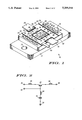
- FIG. 1 is a perspective view of a transistor package which includes a transistor device disposed thereon;
- FIG. 2 is a simplified schematic representation of the transistor package of FIG. 1;
- FIG. 3 is a perspective view of another transistor package of the present invention.
- FIG. 4 is a simplified schematic representation of the package and transistor device of FIG. 3.
- Transistor package 10 for accommodating a transistor chip therein as will be explained.
- Transistor package 10 comprises flange base member 12 made of any suitable thermal conductive metal such as copper and which is typically gold plated.
- Base member 12 includes a pair of mounting holds 14 and 16 formed in the respective ends thereof.
- Isolating substrate 18, which is typically made of beryllium oxide (BeO) and is a generally rectangular form has substantially co-planar top and bottom surfaces.
- the bottom surface of substrate 18 which is metalized is bonded to the upper surface of base member 12 in a conventional manner.
- the top surface of substrate 18 has a selective metalized patterned formed thereon as will be explained.
- the opposing edges 22 and 24 are edge metalized as shown to conductively contact the bottom surface of substrate 18.
- plated through holds 26 and 28 may be utilized to electrically contact edges 22 and 24 to the bottom surface of substrate 18.
- Non-metalized strip areas 30 and 32 insulate edges 22 and 24 from the metalized center portion 20 of substrate 18.
- Center portion 20 has a metalized pad 34 formed in the central area thereof which is isolated from the metalized center portion 20 by non-metalized strip 35 surrounding the pad.
- first and second metalized bonding pads 37 and 39 are formed opposite one another in center portion 20 and are insulated therefrom
- a lead frame comprising leads 36, 38 and 40 is typically brazed to center portion 20 with leads 36 and 38 contacting pads 37 and 39 respectively while lead 40 is brazed to the metalized center portion 20 adjacent and parallel to lead 36.
- Substrate 18, although described as being of beryllium oxide, may be fabricated of any suitable thermally conductive and electrically insulating materials such as aluminum nitrite, sapphire or diamond to name a few.
- Transistor package 10 provides a unique package for providing, for example, forward biased common base transistor operation.
- a transistor chip 42 may be die bonded to pad 34 in which the back side of the chip is its collector electrode while the base and emitter electrodes are disposed on the upper surface of the chip. It is understood that transistor chip 42 is shown for discussion purposes only and is not a true representation of an actual transistor chip.
- a plurality of wire bonds 46 contact the emitter electrodes to lead 36 which forms the external emitter lead of the common base transistor device.
- a plurality of wire bonds 44 connect the base electrodes of the transistor chip to metalized center portion 20 to make direct electrical contact to the DC bias lead 40 while wire bonds 48 electrically connect the collector of transistor 42 to external collector lead 38
- a plurality of MOS chip capacitors 50 having one plate thereof bonded to metalized edges 22 and 24 are contacted via wire bonds 60 and 62 to the metalized center portion 20 and form DC blocking capacitor.
- FIG. 2 shows a simplified schematic diagram of the common base configured transistor package 10 wherein like components therein are referenced by the same reference numerals shown in FIG. 1.
- Wire bonds 60 and 62 are not shown for simplicity but would in fact be in series with bonds 44 between the base electrode of transistor 42 and combined capacitor 50.
- the package has the following features which are advantage over the prior art. Hence, AC bypassing for the base lead (base member 12) is now located within the package itself comprising capacitors 50. This provides a low inductance RF path to ground while the flange base member is the AC (RF) contact for the base of transistor and requires no insulators such as mica or mylar films that are required by the prior art.
- Package 10 also includes a fourth lead (lead 40) that is used only for DC forward biasing of transistor 42. Thus, the AC ground for the device is completely isolated from DC ground.
- package 10 has been described as providing a common base configured transistor package it is well understood that package 10 may be used with a FET to provide a common gate device structure.
- FIGS. 3 and 4 there is shown package 10 of FIG. 1 including input matching for the transistor device Input matching is provided by bonding MOS capacitor 54 to metalized center portion 20 between lead 36 and bonding pad 34.
- the emitter electrodes of transistor die 42 are connected via a plurality of wire bonds 56 and 46 to both capacitor 54 and emitter lead 46 as schematically shown in FIG. 4.
- the impedance at the emitter of transistor 42 can be matched to the input signal impedance that is applied at lead 36.
- output matching can be realized by using a capacitor bonded to metalized center portion 20 between bonding pad 34 and collector lead 38 and wire bonding thereto in the same manner as discussed herein.
- a push-pull or balanced common base configuration could be realized by extending flange member 12 in order to dispose an extended and/or two piece substrate 18 thereon having a plurality of center portions 20 formed on the substrate and isolated from one another to include a pair of transistor chips 42. In this configuration the bases of each transistor chip would be electrically coupled in common to the flange member through a plurality of MOS capacitor chips 50.
- a novel transistor package for RF application which allows configuration of a transistor device as a common base amplifier to be forward bias for linear operation.
- the package allows for internal placement of DC blocking capacitors to facilitate the forward biasing and includes a fourth separate lead for DC biasing only while isolating DC ground from AC ground.
Abstract
Description
Claims (10)
Priority Applications (1)
| Application Number | Priority Date | Filing Date | Title |
|---|---|---|---|
| US07/862,106 US5309014A (en) | 1992-04-02 | 1992-04-02 | Transistor package |
Applications Claiming Priority (1)
| Application Number | Priority Date | Filing Date | Title |
|---|---|---|---|
| US07/862,106 US5309014A (en) | 1992-04-02 | 1992-04-02 | Transistor package |
Publications (1)
| Publication Number | Publication Date |
|---|---|
| US5309014A true US5309014A (en) | 1994-05-03 |
Family
ID=25337675
Family Applications (1)
| Application Number | Title | Priority Date | Filing Date |
|---|---|---|---|
| US07/862,106 Expired - Lifetime US5309014A (en) | 1992-04-02 | 1992-04-02 | Transistor package |
Country Status (1)
| Country | Link |
|---|---|
| US (1) | US5309014A (en) |
Cited By (23)
| Publication number | Priority date | Publication date | Assignee | Title |
|---|---|---|---|---|
| EP0704965A1 (en) * | 1994-08-15 | 1996-04-03 | Texas Instruments Incorporated | Transistor device for super high frequency power amplifiers |
| US5674258A (en) * | 1995-03-08 | 1997-10-07 | Medtronic, Inc. | Packaged integrated accelerometer |
| US5911738A (en) * | 1997-07-31 | 1999-06-15 | Medtronic, Inc. | High output sensor and accelerometer implantable medical device |
| US6020636A (en) * | 1997-10-24 | 2000-02-01 | Eni Technologies, Inc. | Kilowatt power transistor |
| WO2000033378A1 (en) * | 1998-12-02 | 2000-06-08 | Ericsson Inc. | High frequency power transistor device |
| US6459146B2 (en) * | 2000-04-21 | 2002-10-01 | Kabushiki Kaisha Toyoda Jidoshokki Seisakusho | Semiconductor apparatus |
| US6462413B1 (en) * | 1999-07-22 | 2002-10-08 | Polese Company, Inc. | LDMOS transistor heatsink package assembly and manufacturing method |
| US6566749B1 (en) | 2002-01-15 | 2003-05-20 | Fairchild Semiconductor Corporation | Semiconductor die package with improved thermal and electrical performance |
| US20030112090A1 (en) * | 2001-12-18 | 2003-06-19 | Soltan Mehdi Frederik | Internal impedance match in integrated circuits |
| US6621137B1 (en) * | 2000-10-12 | 2003-09-16 | Intel Corporation | MEMS device integrated chip package, and method of making same |
| US6674157B2 (en) | 2001-11-02 | 2004-01-06 | Fairchild Semiconductor Corporation | Semiconductor package comprising vertical power transistor |
| US20040061214A1 (en) * | 2002-09-30 | 2004-04-01 | Cree Microwave, Inc. | Packaged RF power transistor having RF bypassing/output matching network |
| WO2004057666A3 (en) * | 2002-12-19 | 2004-09-10 | Infineon Technologies Ag | Rf power transistor with internal bias feed |
| US20040214419A1 (en) * | 2002-02-28 | 2004-10-28 | Sanyo Electric Co., Ltd. | Semiconductor device and method for manufacturing same |
| CN1309066C (en) * | 2002-02-27 | 2007-04-04 | 三洋电机株式会社 | Semiconductor device |
| WO2007050287A2 (en) * | 2005-10-24 | 2007-05-03 | Freescale Semiconductor, Inc. | Semiconductor structure and method of assembly |
| DE10119474B4 (en) * | 2000-04-21 | 2009-07-30 | Kabushiki Kaisha Toyota Jidoshokki, Kariya | Semiconductor device with leveled rung lengths |
| US20090279220A1 (en) * | 2008-05-06 | 2009-11-12 | Hauenstein Henning M | Semiconductor device package with internal device protection |
| US20100142168A1 (en) * | 2006-01-27 | 2010-06-10 | Freescale Semiconductor, Inc. | Die assemblies |
| US20110011634A1 (en) * | 2009-07-14 | 2011-01-20 | Avago Technologies Enterprise IP (Singapore )Pte. Ltd. | Circuit package with integrated direct-current (dc) blocking capacitor |
| WO2011157171A3 (en) * | 2011-06-03 | 2012-05-03 | 华为技术有限公司 | Insulating ring for packaging, insulating ring assembly, and package |
| US10347571B1 (en) * | 2018-01-09 | 2019-07-09 | Macom Technology Solutions Holdings, Inc. | Intra-package interference isolation |
| US10763639B2 (en) * | 2018-02-12 | 2020-09-01 | Lumentum Operations Llc | Emitter-on-sub-mount device |
Citations (2)
| Publication number | Priority date | Publication date | Assignee | Title |
|---|---|---|---|---|
| US4649416A (en) * | 1984-01-03 | 1987-03-10 | Raytheon Company | Microwave transistor package |
| US5216279A (en) * | 1990-07-26 | 1993-06-01 | Kabushiki Kaisha Toshiba | Power semiconductor device suitable for automation of production |
-
1992
- 1992-04-02 US US07/862,106 patent/US5309014A/en not_active Expired - Lifetime
Patent Citations (2)
| Publication number | Priority date | Publication date | Assignee | Title |
|---|---|---|---|---|
| US4649416A (en) * | 1984-01-03 | 1987-03-10 | Raytheon Company | Microwave transistor package |
| US5216279A (en) * | 1990-07-26 | 1993-06-01 | Kabushiki Kaisha Toshiba | Power semiconductor device suitable for automation of production |
Cited By (37)
| Publication number | Priority date | Publication date | Assignee | Title |
|---|---|---|---|---|
| EP0704965A1 (en) * | 1994-08-15 | 1996-04-03 | Texas Instruments Incorporated | Transistor device for super high frequency power amplifiers |
| US5674258A (en) * | 1995-03-08 | 1997-10-07 | Medtronic, Inc. | Packaged integrated accelerometer |
| US5885471A (en) * | 1995-03-08 | 1999-03-23 | Medtronic, Inc. | Shock resistant accelerometer for implantable medical device |
| US6038475A (en) * | 1995-03-08 | 2000-03-14 | Medtronic, Inc. | High output sensor and accelerometer for implantable medical device |
| US5911738A (en) * | 1997-07-31 | 1999-06-15 | Medtronic, Inc. | High output sensor and accelerometer implantable medical device |
| US6020636A (en) * | 1997-10-24 | 2000-02-01 | Eni Technologies, Inc. | Kilowatt power transistor |
| WO2000033378A1 (en) * | 1998-12-02 | 2000-06-08 | Ericsson Inc. | High frequency power transistor device |
| US6177834B1 (en) | 1998-12-02 | 2001-01-23 | Ericsson, Inc. | Output matched LDMOS power transistor device |
| US6462413B1 (en) * | 1999-07-22 | 2002-10-08 | Polese Company, Inc. | LDMOS transistor heatsink package assembly and manufacturing method |
| DE10119474B4 (en) * | 2000-04-21 | 2009-07-30 | Kabushiki Kaisha Toyota Jidoshokki, Kariya | Semiconductor device with leveled rung lengths |
| US6459146B2 (en) * | 2000-04-21 | 2002-10-01 | Kabushiki Kaisha Toyoda Jidoshokki Seisakusho | Semiconductor apparatus |
| DE10119502B4 (en) * | 2000-04-21 | 2009-08-06 | Kabushiki Kaisha Toyota Jidoshokki, Kariya | Semiconductor device with uniform current paths and small structure |
| US20040016989A1 (en) * | 2000-10-12 | 2004-01-29 | Qing Ma | MEMS device integrated chip package, and method of making same |
| US7291561B2 (en) | 2000-10-12 | 2007-11-06 | Intel Corporation | MEMS device integrated chip package, and method of making same |
| US6621137B1 (en) * | 2000-10-12 | 2003-09-16 | Intel Corporation | MEMS device integrated chip package, and method of making same |
| US6674157B2 (en) | 2001-11-02 | 2004-01-06 | Fairchild Semiconductor Corporation | Semiconductor package comprising vertical power transistor |
| US20040012457A9 (en) * | 2001-12-18 | 2004-01-22 | Soltan Mehdi Frederik | Internal impedance match in integrated circuits |
| US20030112090A1 (en) * | 2001-12-18 | 2003-06-19 | Soltan Mehdi Frederik | Internal impedance match in integrated circuits |
| US6566749B1 (en) | 2002-01-15 | 2003-05-20 | Fairchild Semiconductor Corporation | Semiconductor die package with improved thermal and electrical performance |
| CN1309066C (en) * | 2002-02-27 | 2007-04-04 | 三洋电机株式会社 | Semiconductor device |
| US20040214419A1 (en) * | 2002-02-28 | 2004-10-28 | Sanyo Electric Co., Ltd. | Semiconductor device and method for manufacturing same |
| CN1316609C (en) * | 2002-02-28 | 2007-05-16 | 三洋电机株式会社 | Semiconductor device and its producing method |
| US6906410B2 (en) * | 2002-02-28 | 2005-06-14 | Sanyo Electric Co., Ltd. | Semiconductor device and method for manufacturing same |
| US20040061214A1 (en) * | 2002-09-30 | 2004-04-01 | Cree Microwave, Inc. | Packaged RF power transistor having RF bypassing/output matching network |
| US6822321B2 (en) * | 2002-09-30 | 2004-11-23 | Cree Microwave, Inc. | Packaged RF power transistor having RF bypassing/output matching network |
| WO2004057666A3 (en) * | 2002-12-19 | 2004-09-10 | Infineon Technologies Ag | Rf power transistor with internal bias feed |
| WO2007050287A2 (en) * | 2005-10-24 | 2007-05-03 | Freescale Semiconductor, Inc. | Semiconductor structure and method of assembly |
| US7446411B2 (en) | 2005-10-24 | 2008-11-04 | Freescale Semiconductor, Inc. | Semiconductor structure and method of assembly |
| WO2007050287A3 (en) * | 2005-10-24 | 2009-04-30 | Freescale Semiconductor Inc | Semiconductor structure and method of assembly |
| US20100142168A1 (en) * | 2006-01-27 | 2010-06-10 | Freescale Semiconductor, Inc. | Die assemblies |
| US7989951B2 (en) * | 2006-01-27 | 2011-08-02 | Freescale Semiconductor, Inc. | Die assemblies |
| US20090279220A1 (en) * | 2008-05-06 | 2009-11-12 | Hauenstein Henning M | Semiconductor device package with internal device protection |
| US8102668B2 (en) * | 2008-05-06 | 2012-01-24 | International Rectifier Corporation | Semiconductor device package with internal device protection |
| US20110011634A1 (en) * | 2009-07-14 | 2011-01-20 | Avago Technologies Enterprise IP (Singapore )Pte. Ltd. | Circuit package with integrated direct-current (dc) blocking capacitor |
| WO2011157171A3 (en) * | 2011-06-03 | 2012-05-03 | 华为技术有限公司 | Insulating ring for packaging, insulating ring assembly, and package |
| US10347571B1 (en) * | 2018-01-09 | 2019-07-09 | Macom Technology Solutions Holdings, Inc. | Intra-package interference isolation |
| US10763639B2 (en) * | 2018-02-12 | 2020-09-01 | Lumentum Operations Llc | Emitter-on-sub-mount device |
Similar Documents
| Publication | Publication Date | Title |
|---|---|---|
| US5309014A (en) | Transistor package | |
| US4649416A (en) | Microwave transistor package | |
| US5371405A (en) | High-frequency high-power transistor | |
| US4788584A (en) | RF transistor package with capacitor | |
| EP1145314B1 (en) | High frequency power transistor device | |
| US3936864A (en) | Microwave transistor package | |
| US7342262B2 (en) | Split-gate power module for suppressing oscillation therein | |
| US5166639A (en) | High gain mololithic microwave integrated circuit amplifier | |
| US6777791B2 (en) | Multiple ground signal path LDMOS power package | |
| US4427991A (en) | High frequency semiconductor device | |
| EP0015709B1 (en) | Constructional arrangement for semiconductor devices | |
| US3728589A (en) | Semiconductor assembly | |
| EP0117434A1 (en) | Hybrid microwave subsystem | |
| WO2000075990A1 (en) | High impedance matched rf power transistor | |
| US4975659A (en) | Amplifier package using vertical power transistors with ungrounded common terminals | |
| CA1200017A (en) | Microwave field effect transistor | |
| US6049126A (en) | Semiconductor package and amplifier employing the same | |
| JP2755250B2 (en) | Semiconductor integrated circuit | |
| EP1402628B1 (en) | Stability enhanced multistage power amplifier | |
| JPS6114183Y2 (en) | ||
| US3781613A (en) | Rf transistor carrier | |
| JPH0575314A (en) | Microwave integrated circuit element | |
| JPH06169064A (en) | Semiconductor device | |
| JPH07321130A (en) | Semiconductor device | |
| JPS6114181Y2 (en) |
Legal Events
| Date | Code | Title | Description |
|---|---|---|---|
| AS | Assignment |
Owner name: MOTOROLA, INC. A CORP. OF DELAWARE, ILLINOIS Free format text: ASSIGNMENT OF ASSIGNORS INTEREST.;ASSIGNOR:WILSON, LANCE G.;REEL/FRAME:006086/0035 Effective date: 19920331 |
|
| STCF | Information on status: patent grant |
Free format text: PATENTED CASE |
|
| FPAY | Fee payment |
Year of fee payment: 4 |
|
| FPAY | Fee payment |
Year of fee payment: 8 |
|
| AS | Assignment |
Owner name: FREESCALE SEMICONDUCTOR, INC., TEXAS Free format text: ASSIGNMENT OF ASSIGNORS INTEREST;ASSIGNOR:MOTOROLA, INC.;REEL/FRAME:015698/0657 Effective date: 20040404 Owner name: FREESCALE SEMICONDUCTOR, INC.,TEXAS Free format text: ASSIGNMENT OF ASSIGNORS INTEREST;ASSIGNOR:MOTOROLA, INC.;REEL/FRAME:015698/0657 Effective date: 20040404 |
|
| FPAY | Fee payment |
Year of fee payment: 12 |
|
| AS | Assignment |
Owner name: CITIBANK, N.A. AS COLLATERAL AGENT, NEW YORK Free format text: SECURITY AGREEMENT;ASSIGNORS:FREESCALE SEMICONDUCTOR, INC.;FREESCALE ACQUISITION CORPORATION;FREESCALE ACQUISITION HOLDINGS CORP.;AND OTHERS;REEL/FRAME:018855/0129 Effective date: 20061201 Owner name: CITIBANK, N.A. AS COLLATERAL AGENT,NEW YORK Free format text: SECURITY AGREEMENT;ASSIGNORS:FREESCALE SEMICONDUCTOR, INC.;FREESCALE ACQUISITION CORPORATION;FREESCALE ACQUISITION HOLDINGS CORP.;AND OTHERS;REEL/FRAME:018855/0129 Effective date: 20061201 |
|
| AS | Assignment |
Owner name: CITIBANK, N.A., AS COLLATERAL AGENT,NEW YORK Free format text: SECURITY AGREEMENT;ASSIGNOR:FREESCALE SEMICONDUCTOR, INC.;REEL/FRAME:024397/0001 Effective date: 20100413 Owner name: CITIBANK, N.A., AS COLLATERAL AGENT, NEW YORK Free format text: SECURITY AGREEMENT;ASSIGNOR:FREESCALE SEMICONDUCTOR, INC.;REEL/FRAME:024397/0001 Effective date: 20100413 |
|
| AS | Assignment |
Owner name: FREESCALE SEMICONDUCTOR, INC., TEXAS Free format text: PATENT RELEASE;ASSIGNOR:CITIBANK, N.A., AS COLLATERAL AGENT;REEL/FRAME:037356/0143 Effective date: 20151207 Owner name: FREESCALE SEMICONDUCTOR, INC., TEXAS Free format text: PATENT RELEASE;ASSIGNOR:CITIBANK, N.A., AS COLLATERAL AGENT;REEL/FRAME:037354/0225 Effective date: 20151207 Owner name: FREESCALE SEMICONDUCTOR, INC., TEXAS Free format text: PATENT RELEASE;ASSIGNOR:CITIBANK, N.A., AS COLLATERAL AGENT;REEL/FRAME:037356/0553 Effective date: 20151207 |