EP1547394B1 - Packaged rf power transistor having rf bypassing/output matching network - Google Patents
Packaged rf power transistor having rf bypassing/output matching network Download PDFInfo
- Publication number
- EP1547394B1 EP1547394B1 EP03759357.1A EP03759357A EP1547394B1 EP 1547394 B1 EP1547394 B1 EP 1547394B1 EP 03759357 A EP03759357 A EP 03759357A EP 1547394 B1 EP1547394 B1 EP 1547394B1
- Authority
- EP
- European Patent Office
- Prior art keywords
- transistor
- lead
- packaged
- capacitor
- video
- Prior art date
- Legal status (The legal status is an assumption and is not a legal conclusion. Google has not performed a legal analysis and makes no representation as to the accuracy of the status listed.)
- Expired - Lifetime
Links
Images


Classifications
-
- H—ELECTRICITY
- H03—ELECTRONIC CIRCUITRY
- H03F—AMPLIFIERS
- H03F3/00—Amplifiers with only discharge tubes or only semiconductor devices as amplifying elements
- H03F3/189—High-frequency amplifiers, e.g. radio frequency amplifiers
- H03F3/19—High-frequency amplifiers, e.g. radio frequency amplifiers with semiconductor devices only
- H03F3/195—High-frequency amplifiers, e.g. radio frequency amplifiers with semiconductor devices only in integrated circuits
-
- H—ELECTRICITY
- H03—ELECTRONIC CIRCUITRY
- H03F—AMPLIFIERS
- H03F1/00—Details of amplifiers with only discharge tubes, only semiconductor devices or only unspecified devices as amplifying elements
- H03F1/56—Modifications of input or output impedances, not otherwise provided for
-
- H—ELECTRICITY
- H10—SEMICONDUCTOR DEVICES; ELECTRIC SOLID-STATE DEVICES NOT OTHERWISE PROVIDED FOR
- H10W—GENERIC PACKAGES, INTERCONNECTIONS, CONNECTORS OR OTHER CONSTRUCTIONAL DETAILS OF DEVICES COVERED BY CLASS H10
- H10W44/00—Electrical arrangements for controlling or matching impedance
- H10W44/20—Electrical arrangements for controlling or matching impedance at high-frequency [HF] or radio frequency [RF]
- H10W44/226—Electrical arrangements for controlling or matching impedance at high-frequency [HF] or radio frequency [RF] for HF amplifiers
- H10W44/231—Arrangements for applying bias
Definitions
- This invention relates generally to RF power transistors, and more particularly the invention relates to combining output matching and RF and video bypass circuitry in a packaged RF power transistor.
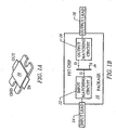
- RF power transistors providing 10 watts or more of power are typically packaged as a discrete device, as shown generally at 10 in Fig. 1A and schematically in Fig. 1B .
- the packaged transistor normally includes an input matching circuit 12 connecting input lead 14 to a gate of a FET (or base of a bipolar transistor) and an output matching circuit 16 connecting output lead 18 to the drain of a FET (or collector or emitter of a bipolar transistor). Normally the source of the FET is grounded.
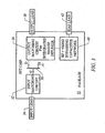
- the packaged transistor is typically mounted on a printed circuit board 20 as shown in Fig. 2 . Also mounted on the printed circuit board are matching circuits 22, 24 and a bias/RF diplexer 26 which connect the transistor output to an RF output. A DC power supply is connected to the transistor output lead through a bias line RF and video bypass circuit 28, diplexer 26, and matching circuit 22.
- This dual function of the printed circuit board circuitry presents a desired impedance transformation at the carrier frequency, and provides a means of injection of DC bias current to the device through the diplexer.
- the circuitry must also properly bypass the power supply connection at RF and video frequencies.
- the distance of the circuitry from the packaged transistor is a limitation in this conventional approach. This separation introduces significant electrical delay, and the inherent characteristics of capacitors used in printed circuit board circuits causes an unavoidable limitation in bias circuit video bandwidth.
- US-A-2002/00220894 (D1) relates to RF passive circuits and RF amplifiers comprising spiral inductors and metal-insulator-metal capacitors.
- the output matching circuit and diplexer along with the RF and video bypassing network are integrated with the power transistor within the transistor package. This places the circuitry closer to the trasnsitor and increases the power supply bypassing video bandwith. Further, the linearity (fidelity) of the power transistor circuit is improved relative to conventional devices for wideband signals.
- discrete multilayer capacitors of the RF and video bypassing network are connected in parallel with a capacitor (with optimal properties at the carrier frequency) of the output matching circuit in an integral arrangement with wire bonding providing inductive elements of the circuitry.
- a wirebond is set to provide a shunt inductive reactance that is equal and opposite to the reactance of the transistor parasitic output capacitance. Additional capacitance for the RF output can be provided also with the RF output providing a bias input or functioning with a separate bias input.
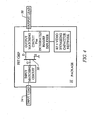
- Figs. 3 and 4 are functional block diagrams of a packaged RF power transistor with matching and bypassing circuitry in accordance with two embodiments of the invention. Like elements in the two figures are the same.
- an RF power transistor 30 is mounted in package 31.
- An FET transistor is illustrated, but as noted above, the power transistor can be bipolar. Further, more than one transistor can be mounted in the package and connected in parallel.
- the gate of FET 30 is connected through input matching circuit 32 to input lead 34, as in the prior art, but the drain is connected through output matching circuit plus integrated bias/RF diplexer 36 to an output lead 38 and to a bias lead 42 which provides DC bias current to the transistor.
- the prior art circuitry illustrated in Fig.
- circuitry 36 and 40 is mounted outside of the package on the printed circuit board at some distance from the transistor.
- the provision of the output matching circuitry, bias/RF diplexer, and RF and video bypassing network within the package increases the power supply bypassing video bandwidth and increases the linearity of the power transistor circuit for wideband signals.
- the functional block diagram of Fig. 4 is similar to the circuit of Fig. 3 except that output lead 38 functions also as the bias lead.
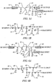
- Figs. 5A, 5B are physical and electrical schematics, respectively, of one embodiment of the invention in which wire bonding is employed as inductive elements and discrete multilayer capacitors are employed in the output matching and by passing networks.
- the input matching circuit 32 of Fig. 3 comprises shunt capacitor 44 connected to the RF input 34 by wire bond 46 and to the base of transistor 30 by wire bond 48.
- the output matching and bypassing network comprises discrete multilayer capacitors 54, 56 connected in parallel with capacitor 50 (which possesses optimal properties at the carrier RF frequency) and which are connected to the drain of transistor 30 and bias input lead 42 by means of wire bonds 52, 58 and 60.
- wire bond 52 comprises an inductance of particular value necessary to resonate with the transistor parasitic output capacitance. This small value supports optimum video bypassing.
- RF output lead 38 is connected to the drain by means of wire bond 62.
- Fig 5B is an electrical schematic of the circuitry of Fig. 5A in which the wire bonds are illustrated as inductive elements in the lumped element schematic.
- Figs. 6A, 6B are physical and electrical schematics of another embodiment of the invention which is similar to the embodiment of Figs. 5A, 5B with the addition of discrete capacitor 64 shunting RF output lead 38 and the drain of transistor 30 to ground and with wire bonds 62, 66 functioning as inductive elements in the output matching network.
- Figs. 7A, 7B are physical and electrical schematics similar to the embodiments of Figs. 5A, 5B but in which a separate bias input lead 42 is not employed.
- the RF output lead 38 functions also as the bias input.
- Figs. 8A, 8B correspond to the embodiment of Figs. 6A, 6B but again a separate bias input is not provided and the RF output 38 functions as the bias input.
- Fig. 9 is a plot of impedance seen at the drain of the transistor at low frequencies versus operating frequency for a conventional device shown at 70 and for a device in accordance with the invention shown at 72.
- the currents flowing from the transistor contain RF (or microwave) frequency components as well as video frequency components.
- the drain would be presented with a perfect power supply, or perfectly RF bypassed power supply, with zero impedance in the video frequency range.
- the common approach to connecting the high current power supply to the drain is to use either a conductor or a high impedance transmission line, sometimes chosen to be 1/4 wavelength at the carrier frequency, with a capacitor bypassing array at the power supply end or connection.
- This array of capacitors is intended to approximate an ideal capacitor, however, actual physical bypass capacitors have inherent internal resistance and internal inductance. Therefore, the typical bypass capacitor array inserts a small capacitor with excellent characteristics at the carrier frequency nearest the transistor, and the larger capacitors (with optimal performance at lower video frequencies) are closer to the power supply. There is necessarily a finite distance between the bypass capacitors, and the short electrical connections also have inductive properties. With real physical capacitors, there are unavoidable resonances in the RF bypass capacitor array. While a low video frequency impedance (typically one ohm) is desired, it often increases to tens of ohms at resonant frequencies.
- a low video frequency impedance typically one ohm
- the present invention increases the frequency of the first significant resonance, while not degrading the carrier frequency characteristics of the circuit, as illustrated in Fig. 9 .
- the first resonance for the conventional circuitry is at about 50 MHz, while the circuitry in accordance with the invention increases the first resonance to approximately to 125 MHz. Since applications of power amplifiers to modern digital communications require very low bias circuit impedance to several tens of MHz, resonances in these circuits must be at frequencies of 100 MHz or higher since the impedance of these circuits shows significant increase at 1/4 the first resonant frequency.
- Fig. 10 shows the complex impedance of the conventional circuit versus the circuit in accordance with the invention on a Smith Chart graph. It is clear that the first resonance of the circuit model with all significant parasitic effects is 52 MHz for the conventional circuit and 127 MHz for the circuit in accordance with the invention. This improvement of over a factor of two is particularly significant for emerging and future digital communications applications where low resonances of conventional circuitry will introduce AM/PM distortion and AM/AM distortion in the output signal. These deleterious effects impair the ability of amplifier linearity enhancement technologies such as predistortion which are critical to these new systems. However, the present invention will make the RF power amplifiers practical in these new technologies.
- Fig. 11 is plot of impedance versus frequency for embodiments of RF power amplifiers where the bias lead is not a separate lead but is included with the RF output lead.
- the bias lead is not a separate lead but is included with the RF output lead.
- an additional resonance 74 is introduced as a hump in the impedance plot 72 and as an extra circle in the Smith Chart representation in Fig. 12 .
- the extra resonance is introduced above 100 MHz, but this single lead alternative is superior to the conventional design which has the resonance at 52 MHz.
- the impedance magnitude is reduced at lower frequencies because there is more combined bypass capacitance.
- RF power amplifiers in which a power supply video bypassing capacitor capacitor network is integrated with existing RF bypass capacitors that exist in a conventional power transistor output matching circuit.
- the total capacitance of the shunt resonant element is thereby increased by a factor of at least 10 relative to the prior art through use of the multiple capacitor network that functions at both RF and video frequencies.
- the invention is applicable to FET and bipolar transistors, both silicon and III-V material, and the invention is applicable to a single transistor or multiple transistors operating in parallel within a single package.
Landscapes
- Engineering & Computer Science (AREA)
- Power Engineering (AREA)
- Microelectronics & Electronic Packaging (AREA)
- Amplifiers (AREA)
Description
- This invention relates generally to RF power transistors, and more particularly the invention relates to combining output matching and RF and video bypass circuitry in a packaged RF power transistor.
- RF power transistors providing 10 watts or more of power are typically packaged as a discrete device, as shown generally at 10 in
Fig. 1A and schematically inFig. 1B . The packaged transistor (FET or bipolar) normally includes aninput matching circuit 12 connectinginput lead 14 to a gate of a FET (or base of a bipolar transistor) and an output matchingcircuit 16 connectingoutput lead 18 to the drain of a FET (or collector or emitter of a bipolar transistor). Normally the source of the FET is grounded. - The packaged transistor is typically mounted on a printed
circuit board 20 as shown inFig. 2 . Also mounted on the printed circuit board are matchingcircuits RF diplexer 26 which connect the transistor output to an RF output. A DC power supply is connected to the transistor output lead through a bias line RF andvideo bypass circuit 28,diplexer 26, andmatching circuit 22. This dual function of the printed circuit board circuitry presents a desired impedance transformation at the carrier frequency, and provides a means of injection of DC bias current to the device through the diplexer. The circuitry must also properly bypass the power supply connection at RF and video frequencies. The distance of the circuitry from the packaged transistor is a limitation in this conventional approach. This separation introduces significant electrical delay, and the inherent characteristics of capacitors used in printed circuit board circuits causes an unavoidable limitation in bias circuit video bandwidth. -
US-A-2002/00220894 - In accordance with the invention, the output matching circuit and diplexer along with the RF and video bypassing network are integrated with the power transistor within the transistor package. This places the circuitry closer to the trasnsitor and increases the power supply bypassing video bandwith. Further, the linearity (fidelity) of the power transistor circuit is improved relative to conventional devices for wideband signals.
- In implementing the invention, discrete multilayer capacitors of the RF and video bypassing network are connected in parallel with a capacitor (with optimal properties at the carrier frequency) of the output matching circuit in an integral arrangement with wire bonding providing inductive elements of the circuitry. Typically a wirebond is set to provide a shunt inductive reactance that is equal and opposite to the reactance of the transistor parasitic output capacitance. Additional capacitance for the RF output can be provided also with the RF output providing a bias input or functioning with a separate bias input.
- The invention and objects and features thereof will be more readily apparent from the following detailed description and dependent claims when taken with the drawings.
-
-
Fig. 1A is a perspective view of a packaged RF power transistor, andFig. 1B is a functional block diagram of the packaged RF power transistor. -
Fig. 2 is a functional block diagram of the packaged RF transistor ofFig. 1 mounted on a printed circuit board along with matching circuitry and bias line RF bypass circuitry for a DC power supply in accordance with prior art. -
Fig. 3 is a functional block diagram of a packaged RF power transistor with matching and bypass circuitry in accordance with an embodiment of an invention. -
Fig. 4 is a functional block diagram of a packaged RF power transistor with matching and bypass circuitry in accordance with another embodiment of the invention. -
Figs. 5A, 5B are physical and electrical schematics of a RF power transistor in accordance with one embodiment of the invention. -
Fig. 6A, 6B are physical and electrical schematics of a RF power transistor in accordance with another embodiment of the invention. -
Fig. 7A, 7B are physical and electrical schematics of a RF power transistor in accordance with another embodiment of the invention. -
Figs. 8A, 8B are physical and electrical schematics of a RF power transistor in accordance with another embodiment of the invention. -
Fig. 9 is a plot of impedance versus frequency for a conventional RF power transistor and a RF power transistor in accordance with an embodiment of the invention. -
Fig. 10 illustrates the complex impedance on a Smith Chart for the transistors used inFig. 9 . -
Fig. 11 is a plot of impedance versus frequency for a conventional RF power transistor and a RF power transistor in accordance with another embodiment of the invention. -
Fig. 12 illustrates the complex impedance on a Smith Chart for the transistors used inFig. 11 . -
Figs. 3 and4 are functional block diagrams of a packaged RF power transistor with matching and bypassing circuitry in accordance with two embodiments of the invention. Like elements in the two figures are the same. InFig. 3 anRF power transistor 30 is mounted inpackage 31. An FET transistor is illustrated, but as noted above, the power transistor can be bipolar. Further, more than one transistor can be mounted in the package and connected in parallel. The gate ofFET 30 is connected throughinput matching circuit 32 toinput lead 34, as in the prior art, but the drain is connected through output matching circuit plus integrated bias/RF diplexer 36 to anoutput lead 38 and to abias lead 42 which provides DC bias current to the transistor. In the prior art circuitry, illustrated inFig. 2 ,circuitry Fig. 4 is similar to the circuit ofFig. 3 except that output lead 38 functions also as the bias lead. -
Figs. 5A, 5B are physical and electrical schematics, respectively, of one embodiment of the invention in which wire bonding is employed as inductive elements and discrete multilayer capacitors are employed in the output matching and by passing networks. InFig. 5A theinput matching circuit 32 ofFig. 3 comprisesshunt capacitor 44 connected to theRF input 34 bywire bond 46 and to the base oftransistor 30 bywire bond 48. The output matching and bypassing network comprisesdiscrete multilayer capacitors transistor 30 andbias input lead 42 by means ofwire bonds wire bond 52 comprises an inductance of particular value necessary to resonate with the transistor parasitic output capacitance. This small value supports optimum video bypassing. Similarly,RF output lead 38 is connected to the drain by means ofwire bond 62. -
Fig 5B is an electrical schematic of the circuitry ofFig. 5A in which the wire bonds are illustrated as inductive elements in the lumped element schematic. -
Figs. 6A, 6B are physical and electrical schematics of another embodiment of the invention which is similar to the embodiment ofFigs. 5A, 5B with the addition ofdiscrete capacitor 64 shuntingRF output lead 38 and the drain oftransistor 30 to ground and withwire bonds -
Figs. 7A, 7B are physical and electrical schematics similar to the embodiments ofFigs. 5A, 5B but in which a separatebias input lead 42 is not employed. The RF output lead 38 functions also as the bias input. Similarly,Figs. 8A, 8B correspond to the embodiment ofFigs. 6A, 6B but again a separate bias input is not provided and theRF output 38 functions as the bias input. -
Fig. 9 is a plot of impedance seen at the drain of the transistor at low frequencies versus operating frequency for a conventional device shown at 70 and for a device in accordance with the invention shown at 72. During normal power amplifier applications with digital communications signals, the currents flowing from the transistor contain RF (or microwave) frequency components as well as video frequency components. In an ideal situation the drain would be presented with a perfect power supply, or perfectly RF bypassed power supply, with zero impedance in the video frequency range. The common approach to connecting the high current power supply to the drain is to use either a conductor or a high impedance transmission line, sometimes chosen to be 1/4 wavelength at the carrier frequency, with a capacitor bypassing array at the power supply end or connection. This array of capacitors is intended to approximate an ideal capacitor, however, actual physical bypass capacitors have inherent internal resistance and internal inductance. Therefore, the typical bypass capacitor array inserts a small capacitor with excellent characteristics at the carrier frequency nearest the transistor, and the larger capacitors (with optimal performance at lower video frequencies) are closer to the power supply. There is necessarily a finite distance between the bypass capacitors, and the short electrical connections also have inductive properties. With real physical capacitors, there are unavoidable resonances in the RF bypass capacitor array. While a low video frequency impedance (typically one ohm) is desired, it often increases to tens of ohms at resonant frequencies. The present invention increases the frequency of the first significant resonance, while not degrading the carrier frequency characteristics of the circuit, as illustrated inFig. 9 . Here the first resonance for the conventional circuitry is at about 50 MHz, while the circuitry in accordance with the invention increases the first resonance to approximately to 125 MHz. Since applications of power amplifiers to modern digital communications require very low bias circuit impedance to several tens of MHz, resonances in these circuits must be at frequencies of 100 MHz or higher since the impedance of these circuits shows significant increase at 1/4 the first resonant frequency. -
Fig. 10 shows the complex impedance of the conventional circuit versus the circuit in accordance with the invention on a Smith Chart graph. It is clear that the first resonance of the circuit model with all significant parasitic effects is 52 MHz for the conventional circuit and 127 MHz for the circuit in accordance with the invention. This improvement of over a factor of two is particularly significant for emerging and future digital communications applications where low resonances of conventional circuitry will introduce AM/PM distortion and AM/AM distortion in the output signal. These deleterious effects impair the ability of amplifier linearity enhancement technologies such as predistortion which are critical to these new systems. However, the present invention will make the RF power amplifiers practical in these new technologies. -
Fig. 11 is plot of impedance versus frequency for embodiments of RF power amplifiers where the bias lead is not a separate lead but is included with the RF output lead. Here there are two RF bypass capacitor networks (internal and external to the package) which can introduce an unwanted extra resonance. As shown inFig. 11 anadditional resonance 74 is introduced as a hump in theimpedance plot 72 and as an extra circle in the Smith Chart representation inFig. 12 . FromFig. 12 it is seen that the extra resonance is introduced above 100 MHz, but this single lead alternative is superior to the conventional design which has the resonance at 52 MHz. Also, the impedance magnitude is reduced at lower frequencies because there is more combined bypass capacitance. - There have been shown several embodiments of RF power amplifiers in which a power supply video bypassing capacitor capacitor network is integrated with existing RF bypass capacitors that exist in a conventional power transistor output matching circuit. The total capacitance of the shunt resonant element is thereby increased by a factor of at least 10 relative to the prior art through use of the multiple capacitor network that functions at both RF and video frequencies. As noted, the invention is applicable to FET and bipolar transistors, both silicon and III-V material, and the invention is applicable to a single transistor or multiple transistors operating in parallel within a single package.
- While the invention has been described with reference to specific embodiments, the description is illustrative of the invention and is not to be construed as limiting the invention. Various other applications and modifications may occur to those skilled in the art without departing from the scope of the invention as defined by the appended claims.
Claims (13)
- A packaged RF power device (31) comprisinga) at least one transistor (30),b) an RF signal input lead (34) coupled to the transistor,c) a ground terminal coupled to the transistor,d) an RF signal output lead (38) coupled to the transistor,e) an output matching circuit (36), comprising a first capacitor (50), and an RF and video bypassing circuit (40), comprising a plurality of discrete multilayer capacitors (54, 56) connected in parallel with the first capacitor, by means of a wire bond (52) coupled to the RF signal output line, andf) a package for housing elements a) and e) with elements b), c), and d) extending from the package.
- The packaged RF power device as defined by claim 1 and further includingg) a bias lead for applying a DC bias voltage through the RF and video bypassing circuit to the transistor.
- The packaged RF power device as defined by claim 2, wherein the RF signal output lead and the bias lead are the same lead.
- The packaged RF power device as defined by any of claims 1 to 3, wherein the RF and video bypassing circuit further comprises wire bonding coupling the plurality of discrete multilayer capacitors to the transistor, the wire bonding providing inductance in the RF bypassing circuit.
- The packaged RF power device as defined by claim 4 wherein the output matching circuit further includes an inductive element with the first capacitor serially connected to ground, and the plurality of discrete multilayer capacitors being connected by wire bonding in parallel with the first capacitor.
- The packaged RF power device as defined by claim 1 wherein the at least one transistor comprises a FET.
- The packaged RF power device as defined by claim 1 wherein the at least one transistor comprises a bipolar transistor.
- The packaged RF power device as defined by claim 1 wherein the at least one transistor comprises a plurality of transistors.
- A method of improving linearity in a wideband RF power transistor device comprising the steps of:a) providing in a housing (10) at least one RF power transistor (30),b) providing an input lead (34) and an output lead (38) extending through the housing and electrically coupled to the transistor,c) providing in the housing an output matching circuit (36), comprising a first capacitor (50), coupled to the output lead, andd) providing in the housing a RF and video bypass circuit (40) connected with the output matching circuit, the RF and video bypass circuit comprising a plurality of discrete multilayer capacitors (54, 56) connected in parallel with the first capacitor by means of a wire bond (52) and preventing RF and video current from flowing to a DC power supply when supplying DC power to the transistor.
- The method as defined by claim 9 and further including the step ofe) providing a bias lead extending through the housing for providing DC power to the transistor, the RF and video bypass circuit being connected to the bias lead.
- The method as defined by claim 10, wherein the RF signal output lead and the bias lead are provided using the same lead.
- The method as defined by any of claims 9 to 11 wherein the RF and video bypass circuit of step d) further comprises wire bonding coupling the plurality of discrete multilayer capacitors to the transistor, the wire bonding providing inductance in the RF bypass circuit.
- The method as defined by claim 12 wherein the output matching circuit of step c) further includes an inductive element with the first capacitor serially connected to ground, and the plurality of discrete multilayer capacitors being connected by wire bonding in parallel with the first capacitor.
Applications Claiming Priority (3)
| Application Number | Priority Date | Filing Date | Title |
|---|---|---|---|
| US10/262,217 US6822321B2 (en) | 2002-09-30 | 2002-09-30 | Packaged RF power transistor having RF bypassing/output matching network |
| US262217 | 2002-09-30 | ||
| PCT/US2003/029719 WO2004032188A2 (en) | 2002-09-30 | 2003-09-17 | Packaged rf power transistor having rf bypassing/output matching network |
Publications (3)
| Publication Number | Publication Date |
|---|---|
| EP1547394A2 EP1547394A2 (en) | 2005-06-29 |
| EP1547394A4 EP1547394A4 (en) | 2006-09-20 |
| EP1547394B1 true EP1547394B1 (en) | 2016-07-27 |
Family
ID=32030167
Family Applications (1)
| Application Number | Title | Priority Date | Filing Date |
|---|---|---|---|
| EP03759357.1A Expired - Lifetime EP1547394B1 (en) | 2002-09-30 | 2003-09-17 | Packaged rf power transistor having rf bypassing/output matching network |
Country Status (7)
| Country | Link |
|---|---|
| US (1) | US6822321B2 (en) |
| EP (1) | EP1547394B1 (en) |
| JP (1) | JP5009500B2 (en) |
| CN (1) | CN1701613B (en) |
| AU (1) | AU2003275086A1 (en) |
| TW (1) | TWI318455B (en) |
| WO (1) | WO2004032188A2 (en) |
Families Citing this family (47)
| Publication number | Priority date | Publication date | Assignee | Title |
|---|---|---|---|---|
| US7109589B2 (en) * | 2004-08-26 | 2006-09-19 | Agere Systems Inc. | Integrated circuit with substantially perpendicular wire bonds |
| US7268627B2 (en) * | 2004-11-03 | 2007-09-11 | Theta Microelectronics, Inc. | Pre-matching of distributed and push-pull power transistors |
| US20060138650A1 (en) * | 2004-12-28 | 2006-06-29 | Freescale Semiconductor, Inc. | Integrated circuit packaging device and method for matching impedance |
| US7193473B2 (en) * | 2005-03-24 | 2007-03-20 | Cree, Inc. | High power Doherty amplifier using multi-stage modules |
| US7564303B2 (en) * | 2005-07-26 | 2009-07-21 | Infineon Technologies Ag | Semiconductor power device and RF signal amplifier |
| US7372334B2 (en) * | 2005-07-26 | 2008-05-13 | Infineon Technologies Ag | Output match transistor |
| US7378920B2 (en) * | 2006-02-14 | 2008-05-27 | Freescale Semiconductor, Inc. | Methods and apparatus for a high-frequency output match circuit |
| EP2013943B1 (en) | 2006-04-26 | 2020-03-25 | Ampleon Netherlands B.V. | A high power integrated rf amplifier |
| US20080231373A1 (en) * | 2007-03-20 | 2008-09-25 | Hafizur Rahman | Output Circuit |
| US8592966B2 (en) * | 2007-06-22 | 2013-11-26 | Cree, Inc. | RF transistor packages with internal stability network including intra-capacitor resistors and methods of forming RF transistor packages with internal stability networks including intra-capacitor resistors |
| US8330265B2 (en) * | 2007-06-22 | 2012-12-11 | Cree, Inc. | RF transistor packages with internal stability network and methods of forming RF transistor packages with internal stability networks |
| US8076994B2 (en) * | 2007-06-22 | 2011-12-13 | Cree, Inc. | RF power transistor packages with internal harmonic frequency reduction and methods of forming RF power transistor packages with internal harmonic frequency reduction |
| JP5030228B2 (en) * | 2007-11-30 | 2012-09-19 | 矢崎総業株式会社 | Electrical junction box |
| WO2009130544A1 (en) * | 2008-04-22 | 2009-10-29 | Freescale Semiconductor, Inc. | Wireless communication unit and semiconductor device having a power amplifier therefor |
| US7948312B2 (en) * | 2009-05-13 | 2011-05-24 | Qualcomm, Incorporated | Multi-bit class-D power amplifier system |
| US8536950B2 (en) * | 2009-08-03 | 2013-09-17 | Qualcomm Incorporated | Multi-stage impedance matching |
| US8102205B2 (en) | 2009-08-04 | 2012-01-24 | Qualcomm, Incorporated | Amplifier module with multiple operating modes |
| US8659359B2 (en) | 2010-04-22 | 2014-02-25 | Freescale Semiconductor, Inc. | RF power transistor circuit |
| EP2388815A1 (en) * | 2010-05-10 | 2011-11-23 | Nxp B.V. | A transistor package |
| USD668658S1 (en) * | 2011-11-15 | 2012-10-09 | Connectblue Ab | Module |
| USD680119S1 (en) * | 2011-11-15 | 2013-04-16 | Connectblue Ab | Module |
| USD692896S1 (en) * | 2011-11-15 | 2013-11-05 | Connectblue Ab | Module |
| USD689053S1 (en) * | 2011-11-15 | 2013-09-03 | Connectblue Ab | Module |
| USD668659S1 (en) * | 2011-11-15 | 2012-10-09 | Connectblue Ab | Module |
| USD680545S1 (en) * | 2011-11-15 | 2013-04-23 | Connectblue Ab | Module |
| US9281283B2 (en) | 2012-09-12 | 2016-03-08 | Freescale Semiconductor, Inc. | Semiconductor devices with impedance matching-circuits |
| EP2802075B1 (en) | 2013-05-07 | 2017-02-15 | Ampleon Netherlands B.V. | Dual-band semiconductor RF amplifier device |
| EP2830089B1 (en) * | 2013-07-25 | 2017-07-12 | Ampleon Netherlands B.V. | RF power device |
| WO2015067985A1 (en) | 2013-11-07 | 2015-05-14 | Freescale Semiconductor, Inc. | Adjustable losses of bond wire arrangement |
| CN105308858B (en) * | 2014-03-21 | 2019-04-05 | 华为技术有限公司 | A power amplifier circuit and transmitter |
| US9515011B2 (en) | 2014-05-28 | 2016-12-06 | Cree, Inc. | Over-mold plastic packaged wide band-gap power transistors and MMICS |
| US9641163B2 (en) | 2014-05-28 | 2017-05-02 | Cree, Inc. | Bandwidth limiting methods for GaN power transistors |
| US9472480B2 (en) | 2014-05-28 | 2016-10-18 | Cree, Inc. | Over-mold packaging for wide band-gap semiconductor devices |
| US9438184B2 (en) | 2014-06-27 | 2016-09-06 | Freescale Semiconductor, Inc. | Integrated passive device assemblies for RF amplifiers, and methods of manufacture thereof |
| CN105322895B (en) * | 2015-05-06 | 2018-11-09 | 苏州能讯高能半导体有限公司 | Matching power tube and the power amplifier module based on the power tube in a kind of biasing is adaptive |
| US10432152B2 (en) | 2015-05-22 | 2019-10-01 | Nxp Usa, Inc. | RF amplifier output circuit device with integrated current path, and methods of manufacture thereof |
| US9571044B1 (en) | 2015-10-21 | 2017-02-14 | Nxp Usa, Inc. | RF power transistors with impedance matching circuits, and methods of manufacture thereof |
| US9692363B2 (en) * | 2015-10-21 | 2017-06-27 | Nxp Usa, Inc. | RF power transistors with video bandwidth circuits, and methods of manufacture thereof |
| CN106206524B (en) * | 2016-07-07 | 2019-01-22 | 昆山华太电子技术有限公司 | A packaging tube shell |
| US10270402B1 (en) * | 2017-11-30 | 2019-04-23 | Nxp Usa, Inc. | Broadband input matching and video bandwidth circuits for power amplifiers |
| US10673386B2 (en) * | 2017-12-05 | 2020-06-02 | Nxp Usa, Inc. | Wideband power amplifiers with harmonic traps |
| US10566938B1 (en) * | 2018-12-11 | 2020-02-18 | Nxp Usa, Inc. | System and method for providing isolation of bias signal from RF signal in integrated circuit |
| CN111510085B (en) * | 2020-05-12 | 2023-06-23 | 苏州远创达科技有限公司 | Output circuit of power amplifier |
| US12230614B2 (en) | 2021-12-17 | 2025-02-18 | Macom Technology Solutions Holdings, Inc. | Multi-typed integrated passive device (IPD) components and devices and processes implementing the same |
| US12183669B2 (en) | 2021-12-17 | 2024-12-31 | Macom Technology Solutions Holdings, Inc. | Configurable metal—insulator—metal capacitor and devices |
| US12417966B2 (en) * | 2021-12-17 | 2025-09-16 | Macom Technology Solutions Holdings, Inc. | IPD components having SiC substrates and devices and processes implementing the same |
| CN120934465B (en) * | 2025-10-16 | 2025-12-26 | 成都屿西半导体科技有限公司 | Radio frequency microwave amplifier for expanding modulation bandwidth |
Family Cites Families (14)
| Publication number | Priority date | Publication date | Assignee | Title |
|---|---|---|---|---|
| JPS58131775A (en) * | 1982-01-29 | 1983-08-05 | Fujitsu Ltd | Field- effect semiconductor device |
| JPH0233963A (en) * | 1988-07-23 | 1990-02-05 | Nec Corp | High frequency transistor |
| JPH03283901A (en) * | 1990-03-30 | 1991-12-13 | Nec Corp | Hybrid microwave integrated circuit |
| US5272450A (en) | 1991-06-20 | 1993-12-21 | Microwave Modules & Devices, Inc. | DC feed network for wideband RF power amplifier |
| US5309014A (en) * | 1992-04-02 | 1994-05-03 | Motorola Inc. | Transistor package |
| US5752182A (en) * | 1994-05-09 | 1998-05-12 | Matsushita Electric Industrial Co., Ltd. | Hybrid IC |
| JPH08222657A (en) * | 1995-02-17 | 1996-08-30 | Hitachi Ltd | Semiconductor integrated circuit device |
| US6675383B1 (en) * | 1997-01-22 | 2004-01-06 | Nielsen Media Research, Inc. | Source detection apparatus and method for audience measurement |
| US6081160A (en) * | 1998-05-20 | 2000-06-27 | Powerwave Technologies, Inc. | Method and apparatus for increasing the bandwidth, and reducing the size, of the DC feed network for wideband RF amplifiers using selective placement of high dielectric constant material |
| US6791419B1 (en) * | 1998-12-02 | 2004-09-14 | Ericsson, Inc. | Constant gain, constant phase RF power block |
| JP4163818B2 (en) * | 1999-07-07 | 2008-10-08 | 三菱電機株式会社 | Internally matched transistor |
| US20020050851A1 (en) * | 1999-12-22 | 2002-05-02 | Grundlingh Johan M. | Method and apparatus for biasing radio frequency power transistors |
| JP4256575B2 (en) * | 2000-08-15 | 2009-04-22 | パナソニック株式会社 | RF passive circuit and RF amplifier with via hole |
| JP2002176368A (en) * | 2001-07-11 | 2002-06-21 | Nec Corp | Transmission power controller capable of controlling optimization of bias current of transmission output amplifier |
-
2002
- 2002-09-30 US US10/262,217 patent/US6822321B2/en not_active Expired - Lifetime
-
2003
- 2003-09-17 JP JP2004541592A patent/JP5009500B2/en not_active Expired - Lifetime
- 2003-09-17 WO PCT/US2003/029719 patent/WO2004032188A2/en not_active Ceased
- 2003-09-17 AU AU2003275086A patent/AU2003275086A1/en not_active Abandoned
- 2003-09-17 EP EP03759357.1A patent/EP1547394B1/en not_active Expired - Lifetime
- 2003-09-17 CN CN038253658A patent/CN1701613B/en not_active Expired - Lifetime
- 2003-09-23 TW TW092126215A patent/TWI318455B/en not_active IP Right Cessation
Non-Patent Citations (1)
| Title |
|---|
| None * |
Also Published As
| Publication number | Publication date |
|---|---|
| JP2006501678A (en) | 2006-01-12 |
| AU2003275086A1 (en) | 2004-04-23 |
| US20040061214A1 (en) | 2004-04-01 |
| TW200408128A (en) | 2004-05-16 |
| CN1701613A (en) | 2005-11-23 |
| WO2004032188A3 (en) | 2004-06-17 |
| AU2003275086A8 (en) | 2004-04-23 |
| WO2004032188A2 (en) | 2004-04-15 |
| EP1547394A2 (en) | 2005-06-29 |
| EP1547394A4 (en) | 2006-09-20 |
| JP5009500B2 (en) | 2012-08-22 |
| US6822321B2 (en) | 2004-11-23 |
| CN1701613B (en) | 2010-10-13 |
| TWI318455B (en) | 2009-12-11 |
Similar Documents
| Publication | Publication Date | Title |
|---|---|---|
| EP1547394B1 (en) | Packaged rf power transistor having rf bypassing/output matching network | |
| US9692363B2 (en) | RF power transistors with video bandwidth circuits, and methods of manufacture thereof | |
| US7119623B2 (en) | Output circuit for a semiconductor amplifier element | |
| US6046641A (en) | Parallel HV MOSFET high power stable amplifier | |
| EP1573813B1 (en) | Rf power transistor with internal bias feed | |
| US7154336B2 (en) | High-frequency power amplifier | |
| US6724263B2 (en) | High-frequency power amplifier | |
| US7508267B1 (en) | GaN based digital controlled broadband MMIC power amplifier | |
| US9929707B1 (en) | Distributed amplifiers with impedance compensation circuits | |
| JP2005516444A (en) | Compensated RF amplifier device | |
| JP2005516444A6 (en) | Compensated RF amplifier device | |
| WO2009060264A1 (en) | Integrated circuit having harmonic termination circuitry | |
| US8299857B2 (en) | RF power amplifier including broadband input matching network | |
| CN107231134A (en) | The LC networks of power amplifier with optional impedance | |
| JPH1093302A (en) | Signal switch | |
| US11309847B2 (en) | Amplifier circuit | |
| US12537483B2 (en) | Amplifier device with low frequency resonance decoupling circuitry | |
| US11677358B2 (en) | Power amplifier circuit | |
| US7199667B2 (en) | Integrated power amplifier arrangement | |
| US12470174B2 (en) | Radiofrequency amplifier | |
| US20250062723A1 (en) | Amplifier devices having multiple bias networks | |
| KR101563212B1 (en) | Semiconductor package for high power transistor | |
| CN116783819A (en) | power amplifier | |
| JP2022512148A (en) | High frequency power transistor and high frequency power amplifier |
Legal Events
| Date | Code | Title | Description |
|---|---|---|---|
| PUAI | Public reference made under article 153(3) epc to a published international application that has entered the european phase |
Free format text: ORIGINAL CODE: 0009012 |
|
| 17P | Request for examination filed |
Effective date: 20050406 |
|
| AK | Designated contracting states |
Kind code of ref document: A2 Designated state(s): AT BE BG CH CY CZ DE DK EE ES FI FR GB GR HU IE IT LI LU MC NL PT RO SE SI SK TR |
|
| AX | Request for extension of the european patent |
Extension state: AL LT LV MK |
|
| DAX | Request for extension of the european patent (deleted) | ||
| RAP1 | Party data changed (applicant data changed or rights of an application transferred) |
Owner name: CREE MICROWAVE, LLC |
|
| A4 | Supplementary search report drawn up and despatched |
Effective date: 20060822 |
|
| 17Q | First examination report despatched |
Effective date: 20061121 |
|
| RAP1 | Party data changed (applicant data changed or rights of an application transferred) |
Owner name: CREE, INC. |
|
| GRAP | Despatch of communication of intention to grant a patent |
Free format text: ORIGINAL CODE: EPIDOSNIGR1 |
|
| INTG | Intention to grant announced |
Effective date: 20160105 |
|
| GRAP | Despatch of communication of intention to grant a patent |
Free format text: ORIGINAL CODE: EPIDOSNIGR1 |
|
| GRAS | Grant fee paid |
Free format text: ORIGINAL CODE: EPIDOSNIGR3 |
|
| GRAA | (expected) grant |
Free format text: ORIGINAL CODE: 0009210 |
|
| INTG | Intention to grant announced |
Effective date: 20160606 |
|
| AK | Designated contracting states |
Kind code of ref document: B1 Designated state(s): AT BE BG CH CY CZ DE DK EE ES FI FR GB GR HU IE IT LI LU MC NL PT RO SE SI SK TR |
|
| REG | Reference to a national code |
Ref country code: GB Ref legal event code: FG4D |
|
| REG | Reference to a national code |
Ref country code: CH Ref legal event code: EP |
|
| REG | Reference to a national code |
Ref country code: AT Ref legal event code: REF Ref document number: 816637 Country of ref document: AT Kind code of ref document: T Effective date: 20160815 |
|
| REG | Reference to a national code |
Ref country code: IE Ref legal event code: FG4D |
|
| REG | Reference to a national code |
Ref country code: DE Ref legal event code: R096 Ref document number: 60349194 Country of ref document: DE |
|
| REG | Reference to a national code |
Ref country code: SE Ref legal event code: TRGR |
|
| REG | Reference to a national code |
Ref country code: NL Ref legal event code: MP Effective date: 20160727 |
|
| REG | Reference to a national code |
Ref country code: AT Ref legal event code: MK05 Ref document number: 816637 Country of ref document: AT Kind code of ref document: T Effective date: 20160727 |
|
| PG25 | Lapsed in a contracting state [announced via postgrant information from national office to epo] |
Ref country code: IT Free format text: LAPSE BECAUSE OF FAILURE TO SUBMIT A TRANSLATION OF THE DESCRIPTION OR TO PAY THE FEE WITHIN THE PRESCRIBED TIME-LIMIT Effective date: 20160727 Ref country code: NL Free format text: LAPSE BECAUSE OF FAILURE TO SUBMIT A TRANSLATION OF THE DESCRIPTION OR TO PAY THE FEE WITHIN THE PRESCRIBED TIME-LIMIT Effective date: 20160727 |
|
| PG25 | Lapsed in a contracting state [announced via postgrant information from national office to epo] |
Ref country code: ES Free format text: LAPSE BECAUSE OF FAILURE TO SUBMIT A TRANSLATION OF THE DESCRIPTION OR TO PAY THE FEE WITHIN THE PRESCRIBED TIME-LIMIT Effective date: 20160727 Ref country code: AT Free format text: LAPSE BECAUSE OF FAILURE TO SUBMIT A TRANSLATION OF THE DESCRIPTION OR TO PAY THE FEE WITHIN THE PRESCRIBED TIME-LIMIT Effective date: 20160727 Ref country code: PT Free format text: LAPSE BECAUSE OF FAILURE TO SUBMIT A TRANSLATION OF THE DESCRIPTION OR TO PAY THE FEE WITHIN THE PRESCRIBED TIME-LIMIT Effective date: 20161128 Ref country code: GR Free format text: LAPSE BECAUSE OF FAILURE TO SUBMIT A TRANSLATION OF THE DESCRIPTION OR TO PAY THE FEE WITHIN THE PRESCRIBED TIME-LIMIT Effective date: 20161028 Ref country code: BE Free format text: LAPSE BECAUSE OF NON-PAYMENT OF DUE FEES Effective date: 20160727 |
|
| REG | Reference to a national code |
Ref country code: DE Ref legal event code: R119 Ref document number: 60349194 Country of ref document: DE |
|
| PG25 | Lapsed in a contracting state [announced via postgrant information from national office to epo] |
Ref country code: EE Free format text: LAPSE BECAUSE OF FAILURE TO SUBMIT A TRANSLATION OF THE DESCRIPTION OR TO PAY THE FEE WITHIN THE PRESCRIBED TIME-LIMIT Effective date: 20160727 Ref country code: RO Free format text: LAPSE BECAUSE OF FAILURE TO SUBMIT A TRANSLATION OF THE DESCRIPTION OR TO PAY THE FEE WITHIN THE PRESCRIBED TIME-LIMIT Effective date: 20160727 Ref country code: MC Free format text: LAPSE BECAUSE OF FAILURE TO SUBMIT A TRANSLATION OF THE DESCRIPTION OR TO PAY THE FEE WITHIN THE PRESCRIBED TIME-LIMIT Effective date: 20160727 |
|
| REG | Reference to a national code |
Ref country code: CH Ref legal event code: PL |
|
| PG25 | Lapsed in a contracting state [announced via postgrant information from national office to epo] |
Ref country code: DK Free format text: LAPSE BECAUSE OF FAILURE TO SUBMIT A TRANSLATION OF THE DESCRIPTION OR TO PAY THE FEE WITHIN THE PRESCRIBED TIME-LIMIT Effective date: 20160727 Ref country code: SK Free format text: LAPSE BECAUSE OF FAILURE TO SUBMIT A TRANSLATION OF THE DESCRIPTION OR TO PAY THE FEE WITHIN THE PRESCRIBED TIME-LIMIT Effective date: 20160727 Ref country code: BG Free format text: LAPSE BECAUSE OF FAILURE TO SUBMIT A TRANSLATION OF THE DESCRIPTION OR TO PAY THE FEE WITHIN THE PRESCRIBED TIME-LIMIT Effective date: 20161027 Ref country code: CZ Free format text: LAPSE BECAUSE OF FAILURE TO SUBMIT A TRANSLATION OF THE DESCRIPTION OR TO PAY THE FEE WITHIN THE PRESCRIBED TIME-LIMIT Effective date: 20160727 |
|
| PLBE | No opposition filed within time limit |
Free format text: ORIGINAL CODE: 0009261 |
|
| STAA | Information on the status of an ep patent application or granted ep patent |
Free format text: STATUS: NO OPPOSITION FILED WITHIN TIME LIMIT |
|
| REG | Reference to a national code |
Ref country code: IE Ref legal event code: MM4A |
|
| REG | Reference to a national code |
Ref country code: FR Ref legal event code: ST Effective date: 20170531 |
|
| 26N | No opposition filed |
Effective date: 20170502 |
|
| PG25 | Lapsed in a contracting state [announced via postgrant information from national office to epo] |
Ref country code: IE Free format text: LAPSE BECAUSE OF NON-PAYMENT OF DUE FEES Effective date: 20160917 Ref country code: DE Free format text: LAPSE BECAUSE OF NON-PAYMENT OF DUE FEES Effective date: 20170401 Ref country code: CH Free format text: LAPSE BECAUSE OF NON-PAYMENT OF DUE FEES Effective date: 20160930 Ref country code: FR Free format text: LAPSE BECAUSE OF NON-PAYMENT OF DUE FEES Effective date: 20160930 Ref country code: LI Free format text: LAPSE BECAUSE OF NON-PAYMENT OF DUE FEES Effective date: 20160930 |
|
| PG25 | Lapsed in a contracting state [announced via postgrant information from national office to epo] |
Ref country code: SI Free format text: LAPSE BECAUSE OF FAILURE TO SUBMIT A TRANSLATION OF THE DESCRIPTION OR TO PAY THE FEE WITHIN THE PRESCRIBED TIME-LIMIT Effective date: 20160727 Ref country code: LU Free format text: LAPSE BECAUSE OF NON-PAYMENT OF DUE FEES Effective date: 20160917 |
|
| PG25 | Lapsed in a contracting state [announced via postgrant information from national office to epo] |
Ref country code: HU Free format text: LAPSE BECAUSE OF FAILURE TO SUBMIT A TRANSLATION OF THE DESCRIPTION OR TO PAY THE FEE WITHIN THE PRESCRIBED TIME-LIMIT; INVALID AB INITIO Effective date: 20030917 Ref country code: CY Free format text: LAPSE BECAUSE OF FAILURE TO SUBMIT A TRANSLATION OF THE DESCRIPTION OR TO PAY THE FEE WITHIN THE PRESCRIBED TIME-LIMIT Effective date: 20160727 |
|
| PG25 | Lapsed in a contracting state [announced via postgrant information from national office to epo] |
Ref country code: TR Free format text: LAPSE BECAUSE OF FAILURE TO SUBMIT A TRANSLATION OF THE DESCRIPTION OR TO PAY THE FEE WITHIN THE PRESCRIBED TIME-LIMIT Effective date: 20160727 |
|
| PGFP | Annual fee paid to national office [announced via postgrant information from national office to epo] |
Ref country code: SE Payment date: 20220927 Year of fee payment: 20 Ref country code: GB Payment date: 20220927 Year of fee payment: 20 Ref country code: FI Payment date: 20220928 Year of fee payment: 20 |
|
| REG | Reference to a national code |
Ref country code: GB Ref legal event code: PE20 Expiry date: 20230916 |
|
| PG25 | Lapsed in a contracting state [announced via postgrant information from national office to epo] |
Ref country code: GB Free format text: LAPSE BECAUSE OF EXPIRATION OF PROTECTION Effective date: 20230916 |
|
| REG | Reference to a national code |
Ref country code: SE Ref legal event code: EUG |