JP4840168B2 - 加熱装置、加熱方法及び記憶媒体 - Google Patents
加熱装置、加熱方法及び記憶媒体 Download PDFInfo
- Publication number
- JP4840168B2 JP4840168B2 JP2007021355A JP2007021355A JP4840168B2 JP 4840168 B2 JP4840168 B2 JP 4840168B2 JP 2007021355 A JP2007021355 A JP 2007021355A JP 2007021355 A JP2007021355 A JP 2007021355A JP 4840168 B2 JP4840168 B2 JP 4840168B2
- Authority
- JP
- Japan
- Prior art keywords
- temperature
- substrate
- heat treatment
- heating chamber
- heating
- Prior art date
- Legal status (The legal status is an assumption and is not a legal conclusion. Google has not performed a legal analysis and makes no representation as to the accuracy of the status listed.)
- Active
Links
Images


Classifications
-
- F—MECHANICAL ENGINEERING; LIGHTING; HEATING; WEAPONS; BLASTING
- F27—FURNACES; KILNS; OVENS; RETORTS
- F27B—FURNACES, KILNS, OVENS, OR RETORTS IN GENERAL; OPEN SINTERING OR LIKE APPARATUS
- F27B17/00—Furnaces of a kind not covered by any preceding group
- F27B17/0016—Chamber type furnaces
- F27B17/0025—Especially adapted for treating semiconductor wafers
-
- H—ELECTRICITY
- H01—ELECTRIC ELEMENTS
- H01L—SEMICONDUCTOR DEVICES NOT COVERED BY CLASS H10
- H01L21/00—Processes or apparatus adapted for the manufacture or treatment of semiconductor or solid state devices or of parts thereof
- H01L21/67—Apparatus specially adapted for handling semiconductor or electric solid state devices during manufacture or treatment thereof; Apparatus specially adapted for handling wafers during manufacture or treatment of semiconductor or electric solid state devices or components ; Apparatus not specifically provided for elsewhere
- H01L21/67005—Apparatus not specifically provided for elsewhere
- H01L21/67011—Apparatus for manufacture or treatment
- H01L21/67098—Apparatus for thermal treatment
- H01L21/67109—Apparatus for thermal treatment mainly by convection
-
- H—ELECTRICITY
- H01—ELECTRIC ELEMENTS
- H01L—SEMICONDUCTOR DEVICES NOT COVERED BY CLASS H10
- H01L21/00—Processes or apparatus adapted for the manufacture or treatment of semiconductor or solid state devices or of parts thereof
- H01L21/67—Apparatus specially adapted for handling semiconductor or electric solid state devices during manufacture or treatment thereof; Apparatus specially adapted for handling wafers during manufacture or treatment of semiconductor or electric solid state devices or components ; Apparatus not specifically provided for elsewhere
- H01L21/67005—Apparatus not specifically provided for elsewhere
- H01L21/67242—Apparatus for monitoring, sorting or marking
- H01L21/67248—Temperature monitoring
-
- H—ELECTRICITY
- H01—ELECTRIC ELEMENTS
- H01L—SEMICONDUCTOR DEVICES NOT COVERED BY CLASS H10
- H01L21/00—Processes or apparatus adapted for the manufacture or treatment of semiconductor or solid state devices or of parts thereof
- H01L21/67—Apparatus specially adapted for handling semiconductor or electric solid state devices during manufacture or treatment thereof; Apparatus specially adapted for handling wafers during manufacture or treatment of semiconductor or electric solid state devices or components ; Apparatus not specifically provided for elsewhere
- H01L21/677—Apparatus specially adapted for handling semiconductor or electric solid state devices during manufacture or treatment thereof; Apparatus specially adapted for handling wafers during manufacture or treatment of semiconductor or electric solid state devices or components ; Apparatus not specifically provided for elsewhere for conveying, e.g. between different workstations
- H01L21/67739—Apparatus specially adapted for handling semiconductor or electric solid state devices during manufacture or treatment thereof; Apparatus specially adapted for handling wafers during manufacture or treatment of semiconductor or electric solid state devices or components ; Apparatus not specifically provided for elsewhere for conveying, e.g. between different workstations into and out of processing chamber
- H01L21/67742—Mechanical parts of transfer devices
-
- H—ELECTRICITY
- H01—ELECTRIC ELEMENTS
- H01L—SEMICONDUCTOR DEVICES NOT COVERED BY CLASS H10
- H01L21/00—Processes or apparatus adapted for the manufacture or treatment of semiconductor or solid state devices or of parts thereof
- H01L21/67—Apparatus specially adapted for handling semiconductor or electric solid state devices during manufacture or treatment thereof; Apparatus specially adapted for handling wafers during manufacture or treatment of semiconductor or electric solid state devices or components ; Apparatus not specifically provided for elsewhere
- H01L21/683—Apparatus specially adapted for handling semiconductor or electric solid state devices during manufacture or treatment thereof; Apparatus specially adapted for handling wafers during manufacture or treatment of semiconductor or electric solid state devices or components ; Apparatus not specifically provided for elsewhere for supporting or gripping
- H01L21/687—Apparatus specially adapted for handling semiconductor or electric solid state devices during manufacture or treatment thereof; Apparatus specially adapted for handling wafers during manufacture or treatment of semiconductor or electric solid state devices or components ; Apparatus not specifically provided for elsewhere for supporting or gripping using mechanical means, e.g. chucks, clamps or pinches
- H01L21/68707—Apparatus specially adapted for handling semiconductor or electric solid state devices during manufacture or treatment thereof; Apparatus specially adapted for handling wafers during manufacture or treatment of semiconductor or electric solid state devices or components ; Apparatus not specifically provided for elsewhere for supporting or gripping using mechanical means, e.g. chucks, clamps or pinches the wafers being placed on a robot blade, or gripped by a gripper for conveyance
Description
この加熱室内に、基板と対向するように設けられた加熱処理用の熱板と、
この熱板を加熱するための加熱手段と、
前記熱板を冷却するための冷却手段と、
前記処理容器内に設けられ、前記加熱室の開口部と隣接する待機位置と、前記熱板に対向する加熱処理位置と、の間で基板を搬送する搬送手段と、
一の基板の加熱処理を終えた後、次の基板が前記加熱室内に搬入される前に熱板を降温させるように前記冷却手段を制御し、次の基板を前記加熱室内に搬入した後、加熱処理温度まで熱板を昇温するように前記加熱手段を制御する動作を、加熱処理される基板毎に繰り返す制御手段と、を備えたことを特徴とする。
前記加熱室に設けられた熱板により、前記加熱室に搬入された基板の表面に形成されたレジスト膜に対し、露光後の加熱処理をする工程と、
一の基板の加熱処理を終えた後、次の基板が前記加熱室に搬入される前に熱板を降温させる工程と、
次の基板を前記加熱室内に搬入した後、加熱処理温度まで熱板を昇温する工程と、を含み、これら熱板を降温させる工程、及び熱板を昇温する工程を、加熱処理される基板毎に繰り返すことを特徴とする。
前記コンピュータプログラムは、上述の何れか一つに記載された加熱方法を実施するようにステップ群が組まれていることを特徴とする。
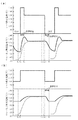
図1〜図4にて説明したものとほぼ同様の構成の加熱処理装置1を用いてウエハWの加熱処理を行い、ウエハW平均温度及びウエハWの先後端間の温度差の経時変化を確認した。実験1では、熱板34、35が130℃の一定温度に加熱された加熱室3内に、12インチのウエハWを30cm/秒の速さで搬入し、上述の各温度の経時変化を計測した。
実験1と同様の加熱処理装置1を用い、熱板34、35の温度を変化させて搬入直後のウエハWの先後端間の温度差の変化を計測した。この他の条件は実験1と同様である。
(実施例) 熱板34、35の温度を105℃とした。
(比較例1)熱板34、35の温度を115℃とした。
(比較例2)熱板34、35の温度を130℃とした。
1 加熱処理装置
2 冷却機構
3 加熱室
4 冷却プレート
5 搬送手段
7 制御部
10 処理容器
10a 搬入出口
10c シャッタ
11 基台
12 ガス吐出部
12a 吐出口
13 ガス供給源
13a ガス供給管
14 伝熱板
14a ヒートパイプ
21a、21b
冷却室
22a、22b
冷媒供給管
23a、23b
冷媒排気管
24 噴出し口
25 排気口
26 冷媒供給源
31 開口部
32 側壁部
33 隙間部
34、35 熱板
34a、35a
ヒータ
36 ヒータコントローラ
41 溝部
42 昇降機構
43 支持ピン
44 切り欠き部
51A、51B
ワイヤ
52A、52B
ワイヤ支持部
53 移動機構
54 基体
55A、55B
ガイドレール
56 駆動部
57 ビーズ部材
58 遮蔽板
61 排気部
61a 排気口
62 ファン
63 排気管
Claims (12)
- 処理容器内に設けられ、側方側の開口部よりほぼ水平に搬入された基板の表面に形成されたレジスト膜に対し、露光後の加熱処理をするための加熱室と、
この加熱室内に、基板と対向するように設けられた加熱処理用の熱板と、
この熱板を加熱するための加熱手段と、
前記熱板を冷却するための冷却手段と、
前記処理容器内に設けられ、前記加熱室の開口部と隣接する待機位置と、前記熱板に対向する加熱処理位置と、の間で基板を搬送する搬送手段と、
一の基板の加熱処理を終えた後、次の基板が前記加熱室内に搬入される前に熱板を降温させるように前記冷却手段を制御し、次の基板を前記加熱室内に搬入した後、加熱処理温度まで熱板を昇温するように前記加熱手段を制御する動作を、加熱処理される基板毎に繰り返す制御手段と、を備えたことを特徴とする加熱処理装置。 - 前記制御手段は、基板が前記加熱室内へ搬入された後、前記熱板を加熱処理温度より高い温度まで昇温し、次いで加熱処理温度に維持するように前記加熱手段を制御することを特徴とする請求項1に記載の加熱処理装置。
- 前記制御手段は、加熱室内の基板の温度が前記処理温度より低い予め設定した温度に到達するタイミングにて、前記加熱手段により熱板を加熱する温度を加熱処理温度より高い温度から加熱処理温度に切り替えることを特徴とする請求項2に記載の加熱処理装置。
- 前記熱板とその加熱手段及び冷却手段とは、前記加熱室内の基板の上面側及び下面側に対向する位置に各々設けられていることを特徴とする請求項1ないし3のいずれか一つに記載の加熱処理装置。
- 前記熱板は、カーボン製であることを特徴とする請求項1ないし4のいずれか一つに記載の加熱処理装置。
- 前記基板は、前記搬送装置により前記加熱室内に搬入された高さ位置のまま加熱処理されることを特徴とする請求項1ないし5のいずれか一つに記載の加熱処理装置。
- 前記搬送手段は、複数本のワイヤであることを特徴とする請求項1ないし6のいずれか一つに記載の加熱処理装置。
- 処理容器内に設けられた加熱室の側方側の開口部よりほぼ水平に基板を搬入する工程と、
前記加熱室に設けられた熱板により、前記加熱室に搬入された基板の表面に形成されたレジスト膜に対し、露光後の加熱処理をする工程と、
一の基板の加熱処理を終えた後、次の基板が前記加熱室に搬入される前に熱板を降温させる工程と、
次の基板を前記加熱室内に搬入した後、加熱処理温度まで熱板を昇温する工程と、を含み、これら熱板を降温させる工程、及び熱板を昇温する工程を、加熱処理される基板毎に繰り返すことを特徴とする基板の加熱処理方法。 - 基板を前記加熱室内に搬入する工程の後、この基板を加熱処理する工程の前に、前記熱板を加熱処理温度より高い温度まで昇温し、次いで加熱処理温度に維持する工程を更に含むことを特徴とする請求項8に記載の基板の加熱処理方法。
- 前記熱板の設定温度は、加熱室内の基板の温度が前記処理温度より低い予め設定した温度に到達するタイミングにて、加熱処理温度より高い温度から加熱処理温度に切り替えられることを特徴とする請求項9に記載の基板の加熱処理方法。
- 前記基板を加熱処理する工程は、当該基板を前記加熱室内に搬入した高さ位置のままで行うことを特徴とする請求項8ないし10のいずれか一つに記載の加熱処理方法。
- 処理容器内に設けられ、側方側から基板を搬入出するための開口部と、この基板を下方側から加熱するように設けられた熱板と、を有する加熱室を備えた加熱装置に用いられるコンピュータプログラムを格納した記憶媒体であって、
前記コンピュータプログラムは、請求項8ないし11の何れか一つに記載された加熱処理方法を実施するようにステップ群が組まれていることを特徴とする記憶媒体。
Priority Applications (3)
| Application Number | Priority Date | Filing Date | Title |
|---|---|---|---|
| JP2007021355A JP4840168B2 (ja) | 2007-01-31 | 2007-01-31 | 加熱装置、加熱方法及び記憶媒体 |
| US12/020,898 US20080182217A1 (en) | 2007-01-31 | 2008-01-28 | Heating device, heating method and storage medium |
| KR1020080009606A KR20080071929A (ko) | 2007-01-31 | 2008-01-30 | 가열 장치, 가열 방법 및 기억 매체 |
Applications Claiming Priority (1)
| Application Number | Priority Date | Filing Date | Title |
|---|---|---|---|
| JP2007021355A JP4840168B2 (ja) | 2007-01-31 | 2007-01-31 | 加熱装置、加熱方法及び記憶媒体 |
Publications (2)
| Publication Number | Publication Date |
|---|---|
| JP2008187126A JP2008187126A (ja) | 2008-08-14 |
| JP4840168B2 true JP4840168B2 (ja) | 2011-12-21 |
Family
ID=39668398
Family Applications (1)
| Application Number | Title | Priority Date | Filing Date |
|---|---|---|---|
| JP2007021355A Active JP4840168B2 (ja) | 2007-01-31 | 2007-01-31 | 加熱装置、加熱方法及び記憶媒体 |
Country Status (3)
| Country | Link |
|---|---|
| US (1) | US20080182217A1 (ja) |
| JP (1) | JP4840168B2 (ja) |
| KR (1) | KR20080071929A (ja) |
Families Citing this family (7)
| Publication number | Priority date | Publication date | Assignee | Title |
|---|---|---|---|---|
| JP4519037B2 (ja) * | 2005-08-31 | 2010-08-04 | 東京エレクトロン株式会社 | 加熱装置及び塗布、現像装置 |
| JP5316135B2 (ja) * | 2009-03-19 | 2013-10-16 | ウシオ電機株式会社 | 露光装置 |
| JP4977747B2 (ja) | 2009-12-10 | 2012-07-18 | 東京エレクトロン株式会社 | 基板の処理方法、プログラム、コンピュータ記憶媒体及び基板処理システム |
| JP6240440B2 (ja) * | 2013-08-30 | 2017-11-29 | 東京応化工業株式会社 | チャンバー装置及び加熱方法 |
| JP6211886B2 (ja) * | 2013-10-15 | 2017-10-11 | 東京エレクトロン株式会社 | 加熱処理方法及び加熱処理装置 |
| JP6926765B2 (ja) * | 2017-07-19 | 2021-08-25 | 東京エレクトロン株式会社 | 基板加熱装置及び基板加熱方法 |
| GB2610156A (en) * | 2021-04-29 | 2023-03-01 | Edwards Ltd | Semiconductor processing system |
Family Cites Families (16)
| Publication number | Priority date | Publication date | Assignee | Title |
|---|---|---|---|---|
| JP4330717B2 (ja) * | 1999-08-09 | 2009-09-16 | 東京エレクトロン株式会社 | ホットプレートユニット及びホットプレートユニットの使用方法 |
| JPS5823722B2 (ja) * | 1978-12-25 | 1983-05-17 | ティーディーケイ株式会社 | 電圧非直線性抵抗体磁器の製造法 |
| JPH01111329A (ja) * | 1987-10-26 | 1989-04-28 | Toshiba Corp | レジスト硬化装置の制御装置 |
| JPH0268921A (ja) * | 1988-09-02 | 1990-03-08 | Tokyo Electron Ltd | レジスト処理装置 |
| JPH03201424A (ja) * | 1989-12-28 | 1991-09-03 | Tokyo Erekutoron Kyushu Kk | 温度制御装置 |
| EP0827186A3 (en) * | 1996-08-29 | 1999-12-15 | Tokyo Electron Limited | Substrate treatment system |
| JPH11173774A (ja) * | 1997-12-05 | 1999-07-02 | Komatsu Ltd | プレート形ヒートパイプ及びこれを用いた温度制御装置 |
| JP2001230199A (ja) * | 1999-07-28 | 2001-08-24 | Komatsu Ltd | 半導体基板の温度制御装置及び熱交換プレート |
| US6600138B2 (en) * | 2001-04-17 | 2003-07-29 | Mattson Technology, Inc. | Rapid thermal processing system for integrated circuits |
| US6887803B2 (en) * | 2001-11-08 | 2005-05-03 | Wafermasters, Inc. | Gas-assisted rapid thermal processing |
| KR100935291B1 (ko) * | 2002-11-28 | 2010-01-06 | 도쿄엘렉트론가부시키가이샤 | 기판 처리 시스템 및 도포 현상 장치 |
| JP2005093949A (ja) * | 2003-09-19 | 2005-04-07 | Dainippon Screen Mfg Co Ltd | 温度調整器、温度調整システムおよび基板処理装置 |
| EP1647789A1 (en) * | 2004-10-04 | 2006-04-19 | Ngk Insulators, Ltd. | Continuous heat treatment furnace and heat treatment method |
| JP4852852B2 (ja) * | 2005-02-17 | 2012-01-11 | ウシオ電機株式会社 | 加熱ユニット |
| JP4535499B2 (ja) * | 2005-04-19 | 2010-09-01 | 東京エレクトロン株式会社 | 加熱装置、塗布、現像装置及び加熱方法 |
| JP4606355B2 (ja) * | 2006-03-14 | 2011-01-05 | 東京エレクトロン株式会社 | 熱処理装置、熱処理方法及び記憶媒体 |
-
2007
- 2007-01-31 JP JP2007021355A patent/JP4840168B2/ja active Active
-
2008
- 2008-01-28 US US12/020,898 patent/US20080182217A1/en not_active Abandoned
- 2008-01-30 KR KR1020080009606A patent/KR20080071929A/ko active Search and Examination
Also Published As
| Publication number | Publication date |
|---|---|
| JP2008187126A (ja) | 2008-08-14 |
| US20080182217A1 (en) | 2008-07-31 |
| KR20080071929A (ko) | 2008-08-05 |
Similar Documents
| Publication | Publication Date | Title |
|---|---|---|
| JP4788610B2 (ja) | 加熱装置、塗布、現像装置、加熱方法及び記憶媒体 | |
| JP4840168B2 (ja) | 加熱装置、加熱方法及び記憶媒体 | |
| US7797855B2 (en) | Heating apparatus, and coating and developing apparatus | |
| JP5195711B2 (ja) | 基板冷却装置、基板冷却方法及び記憶媒体 | |
| JP5101665B2 (ja) | 基板載置台、基板処理装置および基板処理システム | |
| JP4699283B2 (ja) | 熱処理板の温度制御方法、プログラム及び熱処理板の温度制御装置 | |
| KR102503838B1 (ko) | 기판 가열 장치 | |
| KR101227809B1 (ko) | 기판 배치대의 강온 방법, 컴퓨터 판독 가능한 기억 매체, 및 기판 처리 시스템 | |
| JP2006273563A (ja) | ロードロック装置,処理システム及び処理方法 | |
| KR20070122390A (ko) | 기판 처리 방법 및 장치 | |
| KR101667434B1 (ko) | 열 처리 장치, 열 처리 방법 및 기억 매체 | |
| JP3910791B2 (ja) | 基板の熱処理方法及び基板の熱処理装置 | |
| JP6447328B2 (ja) | 加熱装置 | |
| JP2013026509A (ja) | 熱処理装置 | |
| US20060110944A1 (en) | Dummy substrate for thermal reactor | |
| JP4519036B2 (ja) | 加熱装置、塗布、現像装置及び加熱方法 | |
| JP2004235469A (ja) | 熱的処理方法および熱的処理装置 | |
| JP7200638B2 (ja) | 熱処理装置及び熱処理方法 | |
| JPH1163838A (ja) | ハイブリッド型熱処理装置 | |
| KR102282145B1 (ko) | 기판 처리 장치 및 방법 | |
| JPH1022189A (ja) | 基板熱処理装置 | |
| CN109285797B (zh) | 基片加热装置和基片加热方法 | |
| JP2003124134A (ja) | 加熱処理装置および加熱処理方法 | |
| JP2001230201A (ja) | 加熱・冷却処理装置及び方法,基板処理装置 | |
| JP2008166658A (ja) | 熱処理装置 |
Legal Events
| Date | Code | Title | Description |
|---|---|---|---|
| A621 | Written request for application examination |
Free format text: JAPANESE INTERMEDIATE CODE: A621 Effective date: 20090209 |
|
| A131 | Notification of reasons for refusal |
Free format text: JAPANESE INTERMEDIATE CODE: A131 Effective date: 20110412 |
|
| A521 | Request for written amendment filed |
Free format text: JAPANESE INTERMEDIATE CODE: A523 Effective date: 20110613 |
|
| TRDD | Decision of grant or rejection written | ||
| A01 | Written decision to grant a patent or to grant a registration (utility model) |
Free format text: JAPANESE INTERMEDIATE CODE: A01 Effective date: 20110906 |
|
| A01 | Written decision to grant a patent or to grant a registration (utility model) |
Free format text: JAPANESE INTERMEDIATE CODE: A01 |
|
| A61 | First payment of annual fees (during grant procedure) |
Free format text: JAPANESE INTERMEDIATE CODE: A61 Effective date: 20110919 |
|
| R150 | Certificate of patent or registration of utility model |
Ref document number: 4840168 Country of ref document: JP Free format text: JAPANESE INTERMEDIATE CODE: R150 Free format text: JAPANESE INTERMEDIATE CODE: R150 |
|
| FPAY | Renewal fee payment (event date is renewal date of database) |
Free format text: PAYMENT UNTIL: 20141014 Year of fee payment: 3 |
|
| R250 | Receipt of annual fees |
Free format text: JAPANESE INTERMEDIATE CODE: R250 |
|
| R250 | Receipt of annual fees |
Free format text: JAPANESE INTERMEDIATE CODE: R250 |
|
| R250 | Receipt of annual fees |
Free format text: JAPANESE INTERMEDIATE CODE: R250 |
|
| R250 | Receipt of annual fees |
Free format text: JAPANESE INTERMEDIATE CODE: R250 |
|
| R250 | Receipt of annual fees |
Free format text: JAPANESE INTERMEDIATE CODE: R250 |