JP4806803B2 - 金属−セラミックス接合基板およびその製造方法 - Google Patents
金属−セラミックス接合基板およびその製造方法 Download PDFInfo
- Publication number
- JP4806803B2 JP4806803B2 JP2003360846A JP2003360846A JP4806803B2 JP 4806803 B2 JP4806803 B2 JP 4806803B2 JP 2003360846 A JP2003360846 A JP 2003360846A JP 2003360846 A JP2003360846 A JP 2003360846A JP 4806803 B2 JP4806803 B2 JP 4806803B2
- Authority
- JP
- Japan
- Prior art keywords
- metal
- substrate
- ceramic
- ceramic substrate
- metal base
- Prior art date
- Legal status (The legal status is an assumption and is not a legal conclusion. Google has not performed a legal analysis and makes no representation as to the accuracy of the status listed.)
- Expired - Lifetime
Links
Images


Classifications
-
- H—ELECTRICITY
- H01—ELECTRIC ELEMENTS
- H01L—SEMICONDUCTOR DEVICES NOT COVERED BY CLASS H10
- H01L23/00—Details of semiconductor or other solid state devices
- H01L23/12—Mountings, e.g. non-detachable insulating substrates
- H01L23/14—Mountings, e.g. non-detachable insulating substrates characterised by the material or its electrical properties
- H01L23/142—Metallic substrates having insulating layers
-
- H—ELECTRICITY
- H01—ELECTRIC ELEMENTS
- H01L—SEMICONDUCTOR DEVICES NOT COVERED BY CLASS H10
- H01L23/00—Details of semiconductor or other solid state devices
- H01L23/12—Mountings, e.g. non-detachable insulating substrates
- H01L23/13—Mountings, e.g. non-detachable insulating substrates characterised by the shape
-
- H—ELECTRICITY
- H01—ELECTRIC ELEMENTS
- H01L—SEMICONDUCTOR DEVICES NOT COVERED BY CLASS H10
- H01L23/00—Details of semiconductor or other solid state devices
- H01L23/34—Arrangements for cooling, heating, ventilating or temperature compensation ; Temperature sensing arrangements
- H01L23/36—Selection of materials, or shaping, to facilitate cooling or heating, e.g. heatsinks
- H01L23/373—Cooling facilitated by selection of materials for the device or materials for thermal expansion adaptation, e.g. carbon
- H01L23/3735—Laminates or multilayers, e.g. direct bond copper ceramic substrates
-
- H—ELECTRICITY
- H01—ELECTRIC ELEMENTS
- H01L—SEMICONDUCTOR DEVICES NOT COVERED BY CLASS H10
- H01L2924/00—Indexing scheme for arrangements or methods for connecting or disconnecting semiconductor or solid-state bodies as covered by H01L24/00
- H01L2924/0001—Technical content checked by a classifier
- H01L2924/0002—Not covered by any one of groups H01L24/00, H01L24/00 and H01L2224/00
-
- Y—GENERAL TAGGING OF NEW TECHNOLOGICAL DEVELOPMENTS; GENERAL TAGGING OF CROSS-SECTIONAL TECHNOLOGIES SPANNING OVER SEVERAL SECTIONS OF THE IPC; TECHNICAL SUBJECTS COVERED BY FORMER USPC CROSS-REFERENCE ART COLLECTIONS [XRACs] AND DIGESTS
- Y10—TECHNICAL SUBJECTS COVERED BY FORMER USPC
- Y10T—TECHNICAL SUBJECTS COVERED BY FORMER US CLASSIFICATION
- Y10T428/00—Stock material or miscellaneous articles
- Y10T428/12—All metal or with adjacent metals
- Y10T428/12493—Composite; i.e., plural, adjacent, spatially distinct metal components [e.g., layers, joint, etc.]
- Y10T428/12535—Composite; i.e., plural, adjacent, spatially distinct metal components [e.g., layers, joint, etc.] with additional, spatially distinct nonmetal component
- Y10T428/12576—Boride, carbide or nitride component
-
- Y—GENERAL TAGGING OF NEW TECHNOLOGICAL DEVELOPMENTS; GENERAL TAGGING OF CROSS-SECTIONAL TECHNOLOGIES SPANNING OVER SEVERAL SECTIONS OF THE IPC; TECHNICAL SUBJECTS COVERED BY FORMER USPC CROSS-REFERENCE ART COLLECTIONS [XRACs] AND DIGESTS
- Y10—TECHNICAL SUBJECTS COVERED BY FORMER USPC
- Y10T—TECHNICAL SUBJECTS COVERED BY FORMER US CLASSIFICATION
- Y10T428/00—Stock material or miscellaneous articles
- Y10T428/12—All metal or with adjacent metals
- Y10T428/12493—Composite; i.e., plural, adjacent, spatially distinct metal components [e.g., layers, joint, etc.]
- Y10T428/12535—Composite; i.e., plural, adjacent, spatially distinct metal components [e.g., layers, joint, etc.] with additional, spatially distinct nonmetal component
- Y10T428/12611—Oxide-containing component
-
- Y—GENERAL TAGGING OF NEW TECHNOLOGICAL DEVELOPMENTS; GENERAL TAGGING OF CROSS-SECTIONAL TECHNOLOGIES SPANNING OVER SEVERAL SECTIONS OF THE IPC; TECHNICAL SUBJECTS COVERED BY FORMER USPC CROSS-REFERENCE ART COLLECTIONS [XRACs] AND DIGESTS
- Y10—TECHNICAL SUBJECTS COVERED BY FORMER USPC
- Y10T—TECHNICAL SUBJECTS COVERED BY FORMER US CLASSIFICATION
- Y10T428/00—Stock material or miscellaneous articles
- Y10T428/24—Structurally defined web or sheet [e.g., overall dimension, etc.]
- Y10T428/24802—Discontinuous or differential coating, impregnation or bond [e.g., artwork, printing, retouched photograph, etc.]
- Y10T428/24926—Discontinuous or differential coating, impregnation or bond [e.g., artwork, printing, retouched photograph, etc.] including ceramic, glass, porcelain or quartz layer
Description
図1および図2は、本発明による金属−セラミックス接合基板の第1の実施の形態を示している。図1および図2に示すように、本実施の形態の金属−セラミックス接合基板10は、略矩形の平板状のセラミックス基板12と、このセラミックス基板の一方の面に接合し、セラミックス基板12より小さい略矩形の平板状の少なくとも1枚(図1および図2では1枚のみを示す)の回路用金属板14と、セラミックス基板12の他方の面に接合した平面形状が略矩形の放熱用金属ベース板16とから構成されている。本実施の形態では、セラミックス基板12は、約半分の厚さ分だけ金属ベース板16に埋め込まれて金属ベース板16と平行に配置され、金属板14と金属ベース板16とを所定の距離だけ離間させている。
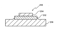
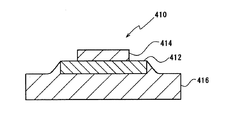
図4は、本発明による金属−セラミックス接合基板の第2の実施の形態を示している。図4に示すように、本実施の形態の金属−セラミックス接合基板110は、略矩形の平板状のセラミックス基板112と、このセラミックス基板の一方の面に接合し、セラミックス基板112より小さい略矩形の平板状の少なくとも1枚(図4では1枚のみを示す)の回路用金属板114と、セラミックス基板112の他方の面に接合した平面形状が略矩形の放熱用金属ベース板116とから構成されている。本実施の形態では、セラミックス基板112は、全ての厚さ分だけ金属ベース板116に埋め込まれて金属ベース板116と平行に配置され、金属板114と金属ベース板116とを所定の距離だけ離間させている。また、セラミックス基板112の金属板114側の面と金属ベース板116の金属板114側の露出面が同一の高さになっている。
第1の実施の形態の金属−セラミックス接合基板の製造方法と同様の方法により、36mm×40mm×0.635mmの窒化アルミニウム基板の一方の面に厚さ0.4mmの3枚のアルミニウム板を接合するとともに、窒化アルミニウム基板が0.3mm程度の厚さ分だけアルミニウムベース板に埋め込まれるように、窒化アルミニウム基板の他方の面に厚さ5mmでのアルミニウムベース板を接合し、第1の実施の形態の金属−セラミックス接合基板と同様の形状の金属−セラミックス接合基板を得た。この金属−セラミックス接合基板に対して、20℃×10分→−40℃×30分→20℃×10分→125℃×30分を1サイクルとするヒートサイクルを3000回行った後に、窒化アルミニウム基板の下側のアルミニウムベース板に亀裂が確認されず、同様のヒートサイクルを5000回行った後にも亀裂が確認されなかった。
第2の実施の形態の金属−セラミックス接合基板の製造方法と同様の方法により、36mm×40mm×0.635mmの窒化アルミニウム基板の窒化アルミニウム基板の一方の面に厚さ0.4mmの3枚のアルミニウム板を接合するとともに、窒化アルミニウム基板が全ての厚さ分だけアルミニウムベース板に埋め込まれるように、窒化アルミニウム基板の他方の面に厚さ5mmでのアルミニウムベース板を接合し、第2の実施の形態の金属−セラミックス接合基板と同様の形状の金属−セラミックス接合基板を得た。この金属−セラミックス接合基板に対して、実施例1と同様のヒートサイクルを3000回行った後に、窒化アルミニウム基板の下側のアルミニウムベース板に亀裂が確認されず、同様のヒートサイクルを5000回行った後にも亀裂が確認されなかった。
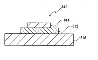
図10に示すように、第1および第2の実施の形態と同様に溶湯法によって、36mm×40mm×0.635mmの窒化アルミニウム基板612の一方の面に厚さ0.4mmの3枚(図5では1枚のみを示す)のアルミニウム板614を接合するとともに、他方の面に厚さ5mmのアルミニウムベース板616を接合し、金属−セラミックス接合基板610を得た。この金属−セラミックス接合基板に対して、実施例1と同様のヒートサイクルを3000回行った後に、窒化アルミニウム基板の下側のアルミニウムベース板に長さ3mmの亀裂が生じた。
12、112、212、312、412、512 セラミックス基板
14、114、214、314、414、514 回路用金属板
16、116、216、316、416、516 放熱用金属ベース板
20、120 鋳型
22、122 下側鋳型部材
22a セラミックス基板保持部
22b、122b 回路用金属板形成部
24、124 上側鋳型部材
24a、124a 金属ベース板形成部
612 窒化アルミニウム基板
614 アルミニウム板
616 アルミニウムベース板
Claims (1)
- 内部にセラミックス基板を配置した鋳型内に金属溶湯を注湯してセラミックス基板の両面に接触させた後に冷却して固化させることにより、セラミックス基板の一方の面に金属板が直接接合するとともに他方の面に放熱用金属ベース部材が直接接合した金属−セラミックス接合基板を製造する方法において、セラミックス基板の一方の面が放熱用金属ベース部材と接触せず且つ他方の面が放熱用金属ベース部材に直接接合するとともにセラミックス基板の側面の少なくとも一部が放熱用金属ベース部材に直接接合するように、セラミックス基板を放熱用金属ベース部材に直接接合することを特徴とする、金属−セラミックス接合基板の製造方法。
Priority Applications (3)
| Application Number | Priority Date | Filing Date | Title |
|---|---|---|---|
| JP2003360846A JP4806803B2 (ja) | 2003-10-21 | 2003-10-21 | 金属−セラミックス接合基板およびその製造方法 |
| US10/969,360 US7122243B2 (en) | 2003-10-21 | 2004-10-19 | Metal/ceramic bonding substrate and method for producing same |
| EP04024974.0A EP1526569B1 (en) | 2003-10-21 | 2004-10-20 | Metal/ceramic bonding substrate and method for producing same |
Applications Claiming Priority (1)
| Application Number | Priority Date | Filing Date | Title |
|---|---|---|---|
| JP2003360846A JP4806803B2 (ja) | 2003-10-21 | 2003-10-21 | 金属−セラミックス接合基板およびその製造方法 |
Publications (2)
| Publication Number | Publication Date |
|---|---|
| JP2005129577A JP2005129577A (ja) | 2005-05-19 |
| JP4806803B2 true JP4806803B2 (ja) | 2011-11-02 |
Family
ID=34386480
Family Applications (1)
| Application Number | Title | Priority Date | Filing Date |
|---|---|---|---|
| JP2003360846A Expired - Lifetime JP4806803B2 (ja) | 2003-10-21 | 2003-10-21 | 金属−セラミックス接合基板およびその製造方法 |
Country Status (3)
| Country | Link |
|---|---|
| US (1) | US7122243B2 (ja) |
| EP (1) | EP1526569B1 (ja) |
| JP (1) | JP4806803B2 (ja) |
Families Citing this family (10)
| Publication number | Priority date | Publication date | Assignee | Title |
|---|---|---|---|---|
| JP4543279B2 (ja) * | 2004-03-31 | 2010-09-15 | Dowaメタルテック株式会社 | アルミニウム接合部材の製造方法 |
| JP2007294891A (ja) * | 2006-03-30 | 2007-11-08 | Dowa Metaltech Kk | 放熱器 |
| WO2008123172A1 (ja) * | 2007-03-27 | 2008-10-16 | Ngk Insulators, Ltd. | ヒートスプレッダモジュール、ヒートシンク及びそれらの製法 |
| JP2008283067A (ja) * | 2007-05-11 | 2008-11-20 | Denso Corp | Al−AlN複合材料及びその製造方法並びに熱交換器 |
| JP2012142371A (ja) * | 2010-12-28 | 2012-07-26 | Mitsubishi Electric Corp | 半導体パッケージ |
| KR101255944B1 (ko) * | 2011-07-20 | 2013-04-23 | 삼성전기주식회사 | 전력 모듈 패키지용 기판 및 그 제조방법 |
| CN106102329B (zh) * | 2016-08-22 | 2019-07-26 | 景旺电子科技(龙川)有限公司 | 一种嵌陶瓷片金属基印制电路板制作方法 |
| US11232991B2 (en) * | 2017-02-23 | 2022-01-25 | Mitsubishi Electric Corporation | Semiconductor apparatus |
| JP2022048812A (ja) * | 2020-09-15 | 2022-03-28 | Dowaメタルテック株式会社 | 放熱部材およびその製造方法 |
| TWI790671B (zh) * | 2021-07-04 | 2023-01-21 | 郭明騰 | 光源模組 |
Family Cites Families (16)
| Publication number | Priority date | Publication date | Assignee | Title |
|---|---|---|---|---|
| JPS63271944A (ja) * | 1987-04-28 | 1988-11-09 | Sumitomo Electric Ind Ltd | 半導体装置 |
| JP2504610B2 (ja) * | 1990-07-26 | 1996-06-05 | 株式会社東芝 | 電力用半導体装置 |
| US5570502A (en) * | 1991-04-08 | 1996-11-05 | Aluminum Company Of America | Fabricating metal matrix composites containing electrical insulators |
| US5602720A (en) * | 1993-06-25 | 1997-02-11 | Sumitomo Electric Industries, Ltd. | Mounting structure for semiconductor device having low thermal resistance |
| US5965193A (en) * | 1994-04-11 | 1999-10-12 | Dowa Mining Co., Ltd. | Process for preparing a ceramic electronic circuit board and process for preparing aluminum or aluminum alloy bonded ceramic material |
| JPH08191120A (ja) * | 1995-01-10 | 1996-07-23 | Hitachi Ltd | パワー半導体素子用基板とその製造方法 |
| JPH08330507A (ja) * | 1995-05-30 | 1996-12-13 | Motorola Inc | ハイブリッド・マルチチップ・モデュールおよびその製造方法 |
| JP3635379B2 (ja) * | 1995-08-04 | 2005-04-06 | 同和鉱業株式会社 | 金属−セラミックス複合基板 |
| WO1998008256A1 (en) * | 1996-08-20 | 1998-02-26 | Kabushiki Kaisha Toshiba | Silicon nitride circuit board and semiconductor module |
| US5944097A (en) * | 1997-05-06 | 1999-08-31 | Northrop Grumman Corporation | Composite substrate carrier for high power electronic devices |
| US6245442B1 (en) * | 1997-05-28 | 2001-06-12 | Kabushiki Kaisha Toyota Chuo | Metal matrix composite casting and manufacturing method thereof |
| JP3449683B2 (ja) * | 1997-12-01 | 2003-09-22 | 電気化学工業株式会社 | セラミックス回路基板とその製造方法 |
| JP4756200B2 (ja) | 2000-09-04 | 2011-08-24 | Dowaメタルテック株式会社 | 金属セラミックス回路基板 |
| JP2003229531A (ja) * | 2002-02-05 | 2003-08-15 | Sanyo Electric Co Ltd | 混成集積回路装置およびその製造方法 |
| JP4133170B2 (ja) * | 2002-09-27 | 2008-08-13 | Dowaホールディングス株式会社 | アルミニウム−セラミックス接合体 |
| US6933443B2 (en) * | 2004-01-28 | 2005-08-23 | Infineon Technologies North America Corp. | Method for bonding ceramic to copper, without creating a bow in the copper |
-
2003
- 2003-10-21 JP JP2003360846A patent/JP4806803B2/ja not_active Expired - Lifetime
-
2004
- 2004-10-19 US US10/969,360 patent/US7122243B2/en active Active
- 2004-10-20 EP EP04024974.0A patent/EP1526569B1/en active Active
Also Published As
| Publication number | Publication date |
|---|---|
| EP1526569A2 (en) | 2005-04-27 |
| EP1526569A3 (en) | 2007-07-18 |
| US7122243B2 (en) | 2006-10-17 |
| US20050084704A1 (en) | 2005-04-21 |
| JP2005129577A (ja) | 2005-05-19 |
| EP1526569B1 (en) | 2019-10-02 |
Similar Documents
| Publication | Publication Date | Title |
|---|---|---|
| US8039757B2 (en) | Electronic part mounting substrate and method for producing same | |
| JP6224960B2 (ja) | 放熱板およびその製造方法 | |
| JP5837754B2 (ja) | 金属−セラミックス接合基板およびその製造方法 | |
| JP4806803B2 (ja) | 金属−セラミックス接合基板およびその製造方法 | |
| JP5619437B2 (ja) | 金属−セラミックス接合基板の製造方法 | |
| JP2017212316A (ja) | 金属−セラミックス接合基板およびその製造方法 | |
| JP2008218938A (ja) | 金属−セラミックス接合基板 | |
| JP4565249B2 (ja) | 金属−セラミックス接合基板およびその製造方法 | |
| JP2010040881A (ja) | 位置決め治具および半導体装置の製造方法 | |
| JP4496404B2 (ja) | 金属−セラミックス接合基板およびその製造方法 | |
| JP5631446B2 (ja) | 金属−セラミックス接合基板の製造方法 | |
| JP5176042B2 (ja) | 電子部品搭載基板の製造装置および製造方法 | |
| JP5389595B2 (ja) | 金属−セラミックス接合基板及びその製造方法 | |
| JP2017228551A (ja) | 金属−セラミックス接合基板およびその製造方法 | |
| JP7157609B2 (ja) | 金属-セラミックス接合基板およびその製造方法 | |
| JP5380734B2 (ja) | アルミニウム接合部材 | |
| JP2011073194A (ja) | 金属−セラミックス接合基板およびその製造方法 | |
| JP7422608B2 (ja) | 金属-セラミックス接合基板およびその製造方法 | |
| JP7267030B2 (ja) | 金属-セラミックス接合基板およびその製造方法 | |
| JP2023074714A (ja) | 金属-セラミックス接合基板およびその製造方法 | |
| JP2022157227A (ja) | 金属-セラミックス接合基板およびその製造方法 | |
| JP2022171255A (ja) | 金属-セラミックス接合基板およびその製造方法 |
Legal Events
| Date | Code | Title | Description |
|---|---|---|---|
| A621 | Written request for application examination |
Free format text: JAPANESE INTERMEDIATE CODE: A621 Effective date: 20060725 |
|
| A977 | Report on retrieval |
Free format text: JAPANESE INTERMEDIATE CODE: A971007 Effective date: 20071221 |
|
| A131 | Notification of reasons for refusal |
Free format text: JAPANESE INTERMEDIATE CODE: A131 Effective date: 20080108 |
|
| A521 | Request for written amendment filed |
Free format text: JAPANESE INTERMEDIATE CODE: A523 Effective date: 20080304 |
|
| A02 | Decision of refusal |
Free format text: JAPANESE INTERMEDIATE CODE: A02 Effective date: 20090616 |
|
| A521 | Request for written amendment filed |
Free format text: JAPANESE INTERMEDIATE CODE: A523 Effective date: 20090909 |
|
| A521 | Request for written amendment filed |
Free format text: JAPANESE INTERMEDIATE CODE: A523 Effective date: 20090914 |
|
| A911 | Transfer to examiner for re-examination before appeal (zenchi) |
Free format text: JAPANESE INTERMEDIATE CODE: A911 Effective date: 20091215 |
|
| A912 | Re-examination (zenchi) completed and case transferred to appeal board |
Free format text: JAPANESE INTERMEDIATE CODE: A912 Effective date: 20100122 |
|
| A521 | Request for written amendment filed |
Free format text: JAPANESE INTERMEDIATE CODE: A523 Effective date: 20110601 |
|
| A711 | Notification of change in applicant |
Free format text: JAPANESE INTERMEDIATE CODE: A712 Effective date: 20110726 |
|
| A01 | Written decision to grant a patent or to grant a registration (utility model) |
Free format text: JAPANESE INTERMEDIATE CODE: A01 |
|
| A61 | First payment of annual fees (during grant procedure) |
Free format text: JAPANESE INTERMEDIATE CODE: A61 Effective date: 20110727 |
|
| A521 | Request for written amendment filed |
Free format text: JAPANESE INTERMEDIATE CODE: A821 Effective date: 20110726 |
|
| FPAY | Renewal fee payment (event date is renewal date of database) |
Free format text: PAYMENT UNTIL: 20140826 Year of fee payment: 3 |
|
| R150 | Certificate of patent or registration of utility model |
Ref document number: 4806803 Country of ref document: JP Free format text: JAPANESE INTERMEDIATE CODE: R150 Free format text: JAPANESE INTERMEDIATE CODE: R150 |
|
| R250 | Receipt of annual fees |
Free format text: JAPANESE INTERMEDIATE CODE: R250 |
|
| R250 | Receipt of annual fees |
Free format text: JAPANESE INTERMEDIATE CODE: R250 |
|
| R250 | Receipt of annual fees |
Free format text: JAPANESE INTERMEDIATE CODE: R250 |
|
| R250 | Receipt of annual fees |
Free format text: JAPANESE INTERMEDIATE CODE: R250 |
|
| R250 | Receipt of annual fees |
Free format text: JAPANESE INTERMEDIATE CODE: R250 |
|
| R250 | Receipt of annual fees |
Free format text: JAPANESE INTERMEDIATE CODE: R250 |
|
| R250 | Receipt of annual fees |
Free format text: JAPANESE INTERMEDIATE CODE: R250 |
|
| R250 | Receipt of annual fees |
Free format text: JAPANESE INTERMEDIATE CODE: R250 |
|
| R250 | Receipt of annual fees |
Free format text: JAPANESE INTERMEDIATE CODE: R250 |