JP4806803B2 - Metal-ceramic bonding substrate and manufacturing method thereof - Google Patents
Metal-ceramic bonding substrate and manufacturing method thereof Download PDFInfo
- Publication number
- JP4806803B2 JP4806803B2 JP2003360846A JP2003360846A JP4806803B2 JP 4806803 B2 JP4806803 B2 JP 4806803B2 JP 2003360846 A JP2003360846 A JP 2003360846A JP 2003360846 A JP2003360846 A JP 2003360846A JP 4806803 B2 JP4806803 B2 JP 4806803B2
- Authority
- JP
- Japan
- Prior art keywords
- metal
- substrate
- ceramic
- ceramic substrate
- metal base
- Prior art date
- Legal status (The legal status is an assumption and is not a legal conclusion. Google has not performed a legal analysis and makes no representation as to the accuracy of the status listed.)
- Expired - Lifetime
Links
Images


Classifications
-
- H—ELECTRICITY
- H01—ELECTRIC ELEMENTS
- H01L—SEMICONDUCTOR DEVICES NOT COVERED BY CLASS H10
- H01L23/00—Details of semiconductor or other solid state devices
- H01L23/12—Mountings, e.g. non-detachable insulating substrates
- H01L23/14—Mountings, e.g. non-detachable insulating substrates characterised by the material or its electrical properties
- H01L23/142—Metallic substrates having insulating layers
-
- H—ELECTRICITY
- H01—ELECTRIC ELEMENTS
- H01L—SEMICONDUCTOR DEVICES NOT COVERED BY CLASS H10
- H01L23/00—Details of semiconductor or other solid state devices
- H01L23/12—Mountings, e.g. non-detachable insulating substrates
- H01L23/13—Mountings, e.g. non-detachable insulating substrates characterised by the shape
-
- H—ELECTRICITY
- H01—ELECTRIC ELEMENTS
- H01L—SEMICONDUCTOR DEVICES NOT COVERED BY CLASS H10
- H01L23/00—Details of semiconductor or other solid state devices
- H01L23/34—Arrangements for cooling, heating, ventilating or temperature compensation ; Temperature sensing arrangements
- H01L23/36—Selection of materials, or shaping, to facilitate cooling or heating, e.g. heatsinks
- H01L23/373—Cooling facilitated by selection of materials for the device or materials for thermal expansion adaptation, e.g. carbon
- H01L23/3735—Laminates or multilayers, e.g. direct bond copper ceramic substrates
-
- H—ELECTRICITY
- H01—ELECTRIC ELEMENTS
- H01L—SEMICONDUCTOR DEVICES NOT COVERED BY CLASS H10
- H01L2924/00—Indexing scheme for arrangements or methods for connecting or disconnecting semiconductor or solid-state bodies as covered by H01L24/00
- H01L2924/0001—Technical content checked by a classifier
- H01L2924/0002—Not covered by any one of groups H01L24/00, H01L24/00 and H01L2224/00
-
- Y—GENERAL TAGGING OF NEW TECHNOLOGICAL DEVELOPMENTS; GENERAL TAGGING OF CROSS-SECTIONAL TECHNOLOGIES SPANNING OVER SEVERAL SECTIONS OF THE IPC; TECHNICAL SUBJECTS COVERED BY FORMER USPC CROSS-REFERENCE ART COLLECTIONS [XRACs] AND DIGESTS
- Y10—TECHNICAL SUBJECTS COVERED BY FORMER USPC
- Y10T—TECHNICAL SUBJECTS COVERED BY FORMER US CLASSIFICATION
- Y10T428/00—Stock material or miscellaneous articles
- Y10T428/12—All metal or with adjacent metals
- Y10T428/12493—Composite; i.e., plural, adjacent, spatially distinct metal components [e.g., layers, joint, etc.]
- Y10T428/12535—Composite; i.e., plural, adjacent, spatially distinct metal components [e.g., layers, joint, etc.] with additional, spatially distinct nonmetal component
- Y10T428/12576—Boride, carbide or nitride component
-
- Y—GENERAL TAGGING OF NEW TECHNOLOGICAL DEVELOPMENTS; GENERAL TAGGING OF CROSS-SECTIONAL TECHNOLOGIES SPANNING OVER SEVERAL SECTIONS OF THE IPC; TECHNICAL SUBJECTS COVERED BY FORMER USPC CROSS-REFERENCE ART COLLECTIONS [XRACs] AND DIGESTS
- Y10—TECHNICAL SUBJECTS COVERED BY FORMER USPC
- Y10T—TECHNICAL SUBJECTS COVERED BY FORMER US CLASSIFICATION
- Y10T428/00—Stock material or miscellaneous articles
- Y10T428/12—All metal or with adjacent metals
- Y10T428/12493—Composite; i.e., plural, adjacent, spatially distinct metal components [e.g., layers, joint, etc.]
- Y10T428/12535—Composite; i.e., plural, adjacent, spatially distinct metal components [e.g., layers, joint, etc.] with additional, spatially distinct nonmetal component
- Y10T428/12611—Oxide-containing component
-
- Y—GENERAL TAGGING OF NEW TECHNOLOGICAL DEVELOPMENTS; GENERAL TAGGING OF CROSS-SECTIONAL TECHNOLOGIES SPANNING OVER SEVERAL SECTIONS OF THE IPC; TECHNICAL SUBJECTS COVERED BY FORMER USPC CROSS-REFERENCE ART COLLECTIONS [XRACs] AND DIGESTS
- Y10—TECHNICAL SUBJECTS COVERED BY FORMER USPC
- Y10T—TECHNICAL SUBJECTS COVERED BY FORMER US CLASSIFICATION
- Y10T428/00—Stock material or miscellaneous articles
- Y10T428/24—Structurally defined web or sheet [e.g., overall dimension, etc.]
- Y10T428/24802—Discontinuous or differential coating, impregnation or bond [e.g., artwork, printing, retouched photograph, etc.]
- Y10T428/24926—Discontinuous or differential coating, impregnation or bond [e.g., artwork, printing, retouched photograph, etc.] including ceramic, glass, porcelain or quartz layer
Description
本発明は、金属−セラミックス接合基板およびその製造方法に関し、特に、セラミックス基板に一方の面に回路用金属板が接合するとともに他方の面に放熱用金属ベース板が接合した金属−セラミックス接合基板およびその製造方法に関する。 The present invention relates to a metal / ceramic bonding substrate and a method for manufacturing the same, and more particularly to a metal / ceramic bonding substrate in which a circuit metal plate is bonded to one surface of a ceramic substrate and a heat dissipation metal base plate is bonded to the other surface. It relates to the manufacturing method.
近年、電気自動車、電車、工作機械などの大電流を制御するためのパワーモジュールの絶縁基板として、セラミックス基板に一方の面に回路用金属板が接合するとともに他方の面に平板状の放熱用金属ベース板が接合した金属−セラミックス接合基板が使用されている(例えば、特許文献1参照)。 In recent years, as a power module insulation board for controlling large currents of electric vehicles, trains, machine tools, etc., a metal plate for circuit is bonded to one side of a ceramic substrate and a flat plate for heat dissipation is used on the other side. A metal / ceramic bonding substrate to which a base plate is bonded is used (see, for example, Patent Document 1).
しかし、従来の金属−セラミックス接合基板では、ヒートサイクルに対する信頼性が必ずしも十分ではない場合があった。 However, the conventional metal / ceramic bonding substrate may not always have sufficient reliability with respect to the heat cycle.
したがって、本発明は、このような従来の問題点に鑑み、ヒートサイクルに対する信頼性を向上させることができる、金属−セラミックス接合基板およびその製造方法を提供することを目的とする。 Therefore, in view of such a conventional problem, an object of the present invention is to provide a metal / ceramic bonding substrate and a method for manufacturing the same, which can improve reliability with respect to heat cycle.
本発明者らは、上記課題を解決するために鋭意研究した結果、セラミックス基板の一方の面に金属板が接合するとともに他方の面に金属ベース部材が接合した金属−セラミックス接合基板において、セラミックス基板の少なくとも一部を金属ベース部材に埋め込むことにより、ヒートサイクルに対する信頼性を向上させることができることを見出し、本発明を完成するに至った。 As a result of intensive studies to solve the above problems, the present inventors have found that a ceramic substrate is a metal-ceramic bonding substrate in which a metal plate is bonded to one surface of a ceramic substrate and a metal base member is bonded to the other surface. It has been found that by embedding at least a part of the metal base member in the metal base member, the reliability with respect to the heat cycle can be improved, and the present invention has been completed.
すなわち、本発明による金属−セラミックス接合基板は、セラミックス基板の一方の面に金属板が接合するとともに他方の面に金属ベース部材が接合した金属−セラミックス接合基板において、セラミックス基板の少なくとも一部が金属ベース部材に埋め込まれていることを特徴とする。この金属−セラミックス接合基板において、セラミックス基板の一部が金属ベース部材に埋め込まれ、セラミックス基板が金属ベース部材と略平行に配置されているのが好ましい。あるいは、セラミックス基板の全ての部分を金属ベース部材に埋め込み、セラミックス基板を金属ベース部材と略平行に配置してもよい。 That is, the metal-ceramic bonding substrate according to the present invention is a metal-ceramic bonding substrate in which a metal plate is bonded to one surface of the ceramic substrate and a metal base member is bonded to the other surface, and at least a part of the ceramic substrate is metal. It is embedded in the base member. In this metal-ceramic bonding substrate, it is preferable that a portion of the ceramic substrate is embedded in the metal base member, and the ceramic substrate is disposed substantially parallel to the metal base member. Alternatively, all parts of the ceramic substrate may be embedded in the metal base member, and the ceramic substrate may be disposed substantially parallel to the metal base member.
また、本発明による金属−セラミックス接合基板は、セラミックス基板の一方の面に金属板が接合するとともに他方の面に金属ベース部材が接合した金属−セラミックス接合基板において、セラミックス基板の側面の少なくとも一部が金属ベース部材に接合していることを特徴とする。この金属−セラミックス接合基板において、セラミックス基板の側面の一部が金属ベース部材に接合し、セラミックス基板が金属ベース部材と略平行に配置されているのが好ましい。あるいは、セラミックス基板の側面の全面を金属ベース部材に接合し、セラミックス基板を金属ベース部材と略平行に配置してもよい。 The metal-ceramic bonding substrate according to the present invention is a metal-ceramic bonding substrate in which a metal plate is bonded to one surface of the ceramic substrate and a metal base member is bonded to the other surface, and at least a part of the side surface of the ceramic substrate. Is bonded to the metal base member. In this metal-ceramic bonding substrate, it is preferable that a part of the side surface of the ceramic substrate is bonded to the metal base member, and the ceramic substrate is arranged substantially parallel to the metal base member. Alternatively, the entire side surface of the ceramic substrate may be bonded to the metal base member, and the ceramic substrate may be disposed substantially parallel to the metal base member.
また、上記の金属−セラミックス接合基板において、金属板がセラミックス基板を介して金属ベース部材から所定の距離だけ離間しているのが好ましい。 In the metal-ceramic bonding substrate, the metal plate is preferably separated from the metal base member by a predetermined distance via the ceramic substrate.
また、本発明による金属−セラミックス接合基板の製造方法は、セラミックス基板の一方の面に金属板が接合するとともに他方の面に金属ベース部材が接合した金属−セラミックス接合基板の製造方法において、セラミックス基板の少なくとも一部が金属ベース部材に埋め込まれるように、あるいは、セラミックス基板の他方の面が金属ベース部材に接合するとともにセラミックス基板の側面の少なくとも一部が金属ベース部材に接合するように、セラミックス基板を金属ベース部材に接合することを特徴とする。これらの金属−セラミックス接合基板の製造方法において、金属板および金属ベース部材の少なくとも一方とセラミックス基板との間の接合が溶湯接合法によって行われるのが好ましい。 The method for manufacturing a metal / ceramic bonding substrate according to the present invention includes a method for manufacturing a metal / ceramic bonding substrate in which a metal plate is bonded to one surface of a ceramic substrate and a metal base member is bonded to the other surface. The ceramic substrate so that at least a part of the ceramic substrate is embedded in the metal base member, or the other surface of the ceramic substrate is bonded to the metal base member and at least a part of the side surface of the ceramic substrate is bonded to the metal base member. Is bonded to a metal base member. In these metal-ceramic bonding substrate manufacturing methods, it is preferable that bonding between at least one of the metal plate and the metal base member and the ceramic substrate is performed by a molten metal bonding method.
さらに、本発明によるパワーモジュールは、上記のいずれかの金属−セラミックス接合基板を用いたことを特徴とする。 Furthermore, the power module according to the present invention is characterized by using any one of the metal-ceramic bonding substrates described above.
本発明によれば、セラミックス基板の一方の面に金属板が接合するとともに他方の面に金属ベース部材が接合した金属−セラミックス接合基板において、セラミックス基板の少なくとも一部を金属ベース部材に埋め込むことにより、ヒートサイクルに対する信頼性を向上させることができる。 According to the present invention, in a metal-ceramic bonding substrate in which a metal plate is bonded to one surface of a ceramic substrate and a metal base member is bonded to the other surface, at least a part of the ceramic substrate is embedded in the metal base member. The reliability with respect to the heat cycle can be improved.
また、従来の金属−セラミックス接合基板と比べて、ヒートサイクル後の金属ベース板のクラックの発生を抑制することができるので、クラックの発生による放熱性の低下を防止することができる。 Moreover, since generation | occurrence | production of the crack of the metal base board after a heat cycle can be suppressed compared with the conventional metal-ceramics bonding board | substrate, the fall of the heat dissipation by generation | occurrence | production of a crack can be prevented.
本発明による金属−セラミックス接合基板の実施の形態では、セラミックス基板の一方の面に金属板が接合するとともに他方の面に金属ベース部材が接合した金属−セラミックス接合基板において、セラミックス基板の少なくとも一部が金属ベース部材に埋め込まれている。 In an embodiment of a metal / ceramic bonding substrate according to the present invention, in a metal / ceramic bonding substrate in which a metal plate is bonded to one surface of a ceramic substrate and a metal base member is bonded to the other surface, at least a part of the ceramic substrate. Is embedded in the metal base member.
なお、セラミックス基板としては、AlN、Al2O3、Si3N4またはSiCを主成分とするセラミックス基板を使用するのが好ましい。また、金属板としては、電気特性や熱伝導性の観点から、アルミニウム、銅またはこれらの合金からなる金属板を使用するのが好ましい。 Incidentally, as the ceramic substrate, AlN, Al 2 O 3, Si 3 preferably used a ceramic substrate mainly composed of N 4 or SiC. Moreover, as a metal plate, it is preferable to use the metal plate which consists of aluminum, copper, or these alloys from an electrical property or a heat conductive viewpoint.
以下、添付図面を参照して、本発明による金属−セラミックス接合基板およびその製造方法の実施の形態について詳細に説明する。 Embodiments of a metal / ceramic bonding substrate and a method for manufacturing the same according to the present invention will be described below in detail with reference to the accompanying drawings.
[第1の実施の形態]
図1および図2は、本発明による金属−セラミックス接合基板の第1の実施の形態を示している。図1および図2に示すように、本実施の形態の金属−セラミックス接合基板10は、略矩形の平板状のセラミックス基板12と、このセラミックス基板の一方の面に接合し、セラミックス基板12より小さい略矩形の平板状の少なくとも1枚(図1および図2では1枚のみを示す)の回路用金属板14と、セラミックス基板12の他方の面に接合した平面形状が略矩形の放熱用金属ベース板16とから構成されている。本実施の形態では、セラミックス基板12は、約半分の厚さ分だけ金属ベース板16に埋め込まれて金属ベース板16と平行に配置され、金属板14と金属ベース板16とを所定の距離だけ離間させている。
[First Embodiment]
1 and 2 show a first embodiment of a metal / ceramic bonding substrate according to the present invention. As shown in FIGS. 1 and 2, a metal /
この実施の形態の金属−セラミックス接合基板10は、例えば、図3に示す鋳型20を用意し、この鋳型20の内部にセラミックス基板12を配置させ、鋳型20の内部に金属溶湯を注湯してセラミックス基板12の両面に接触させた後に冷却して固化させることにより、セラミックス基板12の一方の面に回路用金属板14を接合するとともに他方の面に放熱用金属ベース板16を接合することによって製造することができる。
The metal-
図3に示すように、鋳型20は、平面形状が略矩形のカーボンまたは多孔性金属などの通気性材料からなる下側鋳型部材22と上側鋳型部材24から構成されている。下側鋳型部材22の上面の略中央部には、セラミックス基板12と略等しい平面形状および面積でセラミックス基板12の厚さの約半分の深さのセラミックス基板保持部22aとしての凹部が形成され、このセラミックス基板保持部22aの底面の略中央部には、回路用金属板14と略等しい形状および大きさの回路用金属板形成部22bとしての凹部が形成されている。上側鋳型部材24の内部には、放熱用金属ベース板16と略等しい形状および大きさの金属ベース板形成部24aが形成されている。なお、上側鋳型部材24には、金属溶湯を鋳型20内に注湯するための(図示しない)注湯口が形成されている。また、下側鋳型部材22には、金属ベース板形成部24aと回路用金属板形成部22bとの間に延びる(図示しない)注湯流路が形成され、セラミックス基板保持部22a内にセラミックス基板12を収容したときにも金属ベース板形成部24aと回路用金属板形成部22bとの間が連通するようになっている。
As shown in FIG. 3, the
この鋳型20の下側鋳型部材22のセラミックス基板保持部22a内にセラミックス基板12を収容し、下側鋳型部材22の上に上側鋳型部材24を配置して固定した後、金属ベース板形成部24a内にアルミニウム溶湯などの金属溶湯を注湯し、溶湯流路を介して回路用金属板形成部22bまで金属溶湯を充填し、その後、冷却して金属溶湯を固化させることにより、図1および図2に示す金属−セラミックス接合基板10が得られる。
The
[第2の実施の形態]
図4は、本発明による金属−セラミックス接合基板の第2の実施の形態を示している。図4に示すように、本実施の形態の金属−セラミックス接合基板110は、略矩形の平板状のセラミックス基板112と、このセラミックス基板の一方の面に接合し、セラミックス基板112より小さい略矩形の平板状の少なくとも1枚(図4では1枚のみを示す)の回路用金属板114と、セラミックス基板112の他方の面に接合した平面形状が略矩形の放熱用金属ベース板116とから構成されている。本実施の形態では、セラミックス基板112は、全ての厚さ分だけ金属ベース板116に埋め込まれて金属ベース板116と平行に配置され、金属板114と金属ベース板116とを所定の距離だけ離間させている。また、セラミックス基板112の金属板114側の面と金属ベース板116の金属板114側の露出面が同一の高さになっている。
[Second Embodiment]
FIG. 4 shows a second embodiment of the metal / ceramic bonding substrate according to the present invention. As shown in FIG. 4, the metal /
この実施の形態の金属−セラミックス接合基板110は、例えば、図5に示す鋳型120を用意し、この鋳型120の内部にセラミックス基板112を配置させ、鋳型120の内部に金属溶湯を注湯してセラミックス基板112の両面に接触させた後に冷却して固化させることにより、セラミックス基板112の一方の面に回路用金属板114を接合するとともに他方の面に放熱用金属ベース板116を接合することによって製造することができる。
The metal-
図5に示すように、鋳型120は、平面形状が略矩形のカーボンまたは多孔性金属などの通気性材料からなる下側鋳型部材122と上側鋳型部材124から構成されている。下側鋳型部材122の上面の略中央部には、回路用金属板114と略等しい形状および大きさの回路用金属板形成部122bとしての凹部が形成され、この回路用金属板形成部122bの上にセラミックス基板112が配置されるようになっている。また、上側鋳型部材124の内部には、セラミックス基板112が埋め込まれる放熱用金属ベース板116と略等しい形状および大きさの金属ベース板形成部124aが形成されている。なお、上側鋳型部材124には、金属溶湯を鋳型120内に注湯するための(図示しない)注湯口が形成されている。また、下側鋳型部材122には、金属ベース板形成部124aと回路用金属板形成部122bとの間に延びる(図示しない)注湯流路が形成され、回路用金属板形成部122bの上にセラミックス基板112が配置されたときにも金属ベース板形成部124aと回路用金属板形成部122bとの間が連通するようになっている。
As shown in FIG. 5, the
なお、下側鋳型部材122の上面のセラミックス基板112の各側面に対応する部分に、セラミックス基板112の位置決め用の(図示しない)微小の突起またはリブを設け、これらの突起またはリブに囲まれた領域内にセラミックス基板112を配置するのが好ましい。また、これらの突起またはリブは、ヒートサイクル後にクラックが発生し易いセラミックス基板112の角部が放熱用金属ベース板116で覆われるように、セラミックス基板112の角部に対応する部分を除いた各側面の略中央に対応する部分に設けるのが好ましい。
In addition, minute projections or ribs (not shown) for positioning the
この鋳型120の下側鋳型部材22の回路用金属板形成部122bの上の所定の位置にセラミックス基板112を配置させ、下側鋳型部材122の上に上側鋳型部材124を配置して固定した後、金属ベース板形成部124a内にアルミニウム溶湯などの金属溶湯を注湯し、溶湯流路を介して回路用金属板形成部122bまで金属溶湯を充填し、その後、冷却して金属溶湯を固化させることにより、図4に示す金属−セラミックス接合基板110が得られる。
After the
このようにして製造した第1または第2の実施の形態の金属−セラミックス接合基板は、回路用金属板に回路パターンを形成した後、パワーモジュール用のセラミックス回路基板や、半導体実装用のセラミックス回路基板として使用することができる。例えば、このようにして製造された金属−セラミックス接合回路基板を用いて、Siチップなどの半導体チップの半田付け、アルミワイヤのボンディングなどによる配線、プラスチックパッケージの接着などのアセンブリ工程を経て、ヒートサイクルに対する信頼性の高いパワーモジュールを得ることができる。 The metal-ceramic bonding substrate according to the first or second embodiment manufactured in this way is formed with a circuit pattern on a circuit metal plate, and then a ceramic circuit substrate for a power module or a ceramic circuit for semiconductor mounting. It can be used as a substrate. For example, the metal-ceramic bonding circuit board manufactured in this way is used for heat cycle through assembly processes such as soldering of semiconductor chips such as Si chips, wiring by bonding of aluminum wires, and adhesion of plastic packages. A highly reliable power module can be obtained.
なお、上記の第1および第2の実施の形態では、金属−セラミックス接合基板を溶湯法によって製造する場合について説明したが、本発明による金属−セラミックス接合基板は、ろう接法や直接接合法などの他の方法によって製造してもよい。 In the first and second embodiments described above, the case where the metal / ceramic bonding substrate is manufactured by the molten metal method has been described. However, the metal / ceramic bonding substrate according to the present invention includes a brazing method and a direct bonding method. It may be manufactured by other methods.
また、上記の第1および第2の実施の形態では、放熱用金属ベース板の形状が略平板状であり、そのセラミックス基板と反対側の面(裏面)が平面状であったが、本発明による金属−セラミックス接合基板では、裏面にフィンが形成されたフィン付ベース板や内部に水冷用の水路が設けられた水冷ベース板などを放熱用金属ベース板として使用してもよい。このような金属ベース板を使用しても、上記の第1および第2の実施の形態と同様の効果が得られる。また、上記の第1および第2の実施の形態では、回路用金属板が1枚の場合について図示して説明したが、回路用金属板が複数の場合でも同様の効果が得られる。 In the first and second embodiments described above, the shape of the metal base plate for heat dissipation is substantially flat, and the surface (back surface) opposite to the ceramic substrate is planar. In the metal-ceramic bonding substrate according to, a fin-equipped base plate with fins formed on the back surface, a water-cooled base plate with water-cooling water channels provided therein, or the like may be used as the heat-dissipating metal base plate. Even if such a metal base plate is used, the same effects as those of the first and second embodiments can be obtained. In the first and second embodiments described above, the case where there is one circuit metal plate is illustrated and described, but the same effect can be obtained even when there are a plurality of circuit metal plates.
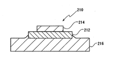
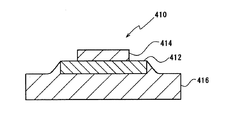
また、上記の第1および第2の実施の形態では、放熱用金属ベース板の金属板側の面のセラミックス基板のまわりの部分が平面であったが、本発明による金属−セラミックス接合基板では、図6〜図9に示すように、放熱用金属ベース板がセラミックス基板の周囲を取り囲んでセラミックス基板の側面の一部または全部に接合するように、放熱用金属ベース板の金属板側の面に滑らかな隆起部または階段状の隆起部を設けてもよい。このように、セラミックス基板の側面の少なくとも一部が放熱用金属ベース板に接合していれば、上記の第1および第2の実施の形態と同様の効果が得られる。なお、図6〜図9において、参照符号210、310、410および510は金属−セラミックス接合基板、参照符号212、312、412および512はセラミックス基板、参照符号214、314、414および514は回路用金属板、参照符号216、316、416および516は放熱用金属ベース板を示す。
In the first and second embodiments described above, the portion around the ceramic substrate on the metal plate side surface of the heat radiating metal base plate is a flat surface. However, in the metal-ceramic bonding substrate according to the present invention, As shown in FIG. 6 to FIG. 9, on the surface of the metal plate side of the heat dissipation metal base plate so that the metal base plate for heat dissipation surrounds the periphery of the ceramic substrate and is joined to part or all of the side surface of the ceramic substrate. A smooth ridge or stepped ridge may be provided. Thus, if at least a part of the side surface of the ceramic substrate is bonded to the metal base plate for heat dissipation, the same effect as the first and second embodiments can be obtained. 6 to 9,
[実施例1]
第1の実施の形態の金属−セラミックス接合基板の製造方法と同様の方法により、36mm×40mm×0.635mmの窒化アルミニウム基板の一方の面に厚さ0.4mmの3枚のアルミニウム板を接合するとともに、窒化アルミニウム基板が0.3mm程度の厚さ分だけアルミニウムベース板に埋め込まれるように、窒化アルミニウム基板の他方の面に厚さ5mmでのアルミニウムベース板を接合し、第1の実施の形態の金属−セラミックス接合基板と同様の形状の金属−セラミックス接合基板を得た。この金属−セラミックス接合基板に対して、20℃×10分→−40℃×30分→20℃×10分→125℃×30分を1サイクルとするヒートサイクルを3000回行った後に、窒化アルミニウム基板の下側のアルミニウムベース板に亀裂が確認されず、同様のヒートサイクルを5000回行った後にも亀裂が確認されなかった。
[Example 1]
Three aluminum plates having a thickness of 0.4 mm are bonded to one surface of a 36 mm × 40 mm × 0.635 mm aluminum nitride substrate by a method similar to the method for manufacturing the metal / ceramic bonding substrate of the first embodiment. In addition, an aluminum base plate having a thickness of 5 mm is joined to the other surface of the aluminum nitride substrate so that the aluminum nitride substrate is embedded in the aluminum base plate by a thickness of about 0.3 mm. A metal-ceramic bonding substrate having the same shape as that of the metal-ceramic bonding substrate in the form was obtained. The metal-ceramic bonding substrate was subjected to a heat cycle 3000 times of 20 ° C. × 10 minutes → −40 ° C. × 30 minutes → 20 ° C. × 10 minutes → 125 ° C. × 30 minutes, and then aluminum nitride. No crack was confirmed in the aluminum base plate on the lower side of the substrate, and no crack was confirmed even after 5000 heat cycles were performed.
[実施例2]
第2の実施の形態の金属−セラミックス接合基板の製造方法と同様の方法により、36mm×40mm×0.635mmの窒化アルミニウム基板の窒化アルミニウム基板の一方の面に厚さ0.4mmの3枚のアルミニウム板を接合するとともに、窒化アルミニウム基板が全ての厚さ分だけアルミニウムベース板に埋め込まれるように、窒化アルミニウム基板の他方の面に厚さ5mmでのアルミニウムベース板を接合し、第2の実施の形態の金属−セラミックス接合基板と同様の形状の金属−セラミックス接合基板を得た。この金属−セラミックス接合基板に対して、実施例1と同様のヒートサイクルを3000回行った後に、窒化アルミニウム基板の下側のアルミニウムベース板に亀裂が確認されず、同様のヒートサイクルを5000回行った後にも亀裂が確認されなかった。
[Example 2]
By a method similar to the method of manufacturing the metal / ceramic bonding substrate of the second embodiment, three sheets of 0.4 mm thick are formed on one surface of an aluminum nitride substrate of 36 mm × 40 mm × 0.635 mm. In the second embodiment, the aluminum plate is bonded, and an aluminum base plate having a thickness of 5 mm is bonded to the other surface of the aluminum nitride substrate so that the aluminum nitride substrate is embedded in the aluminum base plate by the entire thickness. A metal-ceramic bonding substrate having the same shape as that of the metal-ceramic bonding substrate of the form was obtained. After the same heat cycle as in Example 1 was performed 3000 times on this metal-ceramic bonding substrate, no crack was confirmed in the lower aluminum base plate of the aluminum nitride substrate, and the same heat cycle was performed 5000 times. No cracks were observed after a while.
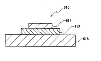
[比較例]
図10に示すように、第1および第2の実施の形態と同様に溶湯法によって、36mm×40mm×0.635mmの窒化アルミニウム基板612の一方の面に厚さ0.4mmの3枚(図5では1枚のみを示す)のアルミニウム板614を接合するとともに、他方の面に厚さ5mmのアルミニウムベース板616を接合し、金属−セラミックス接合基板610を得た。この金属−セラミックス接合基板に対して、実施例1と同様のヒートサイクルを3000回行った後に、窒化アルミニウム基板の下側のアルミニウムベース板に長さ3mmの亀裂が生じた。
[Comparative example]
As shown in FIG. 10, three pieces of 0.4 mm thick (FIG. 10) are formed on one surface of an
10、110、210、310、410、510、610 金属−セラミックス接合基板
12、112、212、312、412、512 セラミックス基板
14、114、214、314、414、514 回路用金属板
16、116、216、316、416、516 放熱用金属ベース板
20、120 鋳型
22、122 下側鋳型部材
22a セラミックス基板保持部
22b、122b 回路用金属板形成部
24、124 上側鋳型部材
24a、124a 金属ベース板形成部
612 窒化アルミニウム基板
614 アルミニウム板
616 アルミニウムベース板
10, 110, 210, 310, 410, 510, 610 Metal-
Claims (1)
Priority Applications (3)
| Application Number | Priority Date | Filing Date | Title |
|---|---|---|---|
| JP2003360846A JP4806803B2 (en) | 2003-10-21 | 2003-10-21 | Metal-ceramic bonding substrate and manufacturing method thereof |
| US10/969,360 US7122243B2 (en) | 2003-10-21 | 2004-10-19 | Metal/ceramic bonding substrate and method for producing same |
| EP04024974.0A EP1526569B1 (en) | 2003-10-21 | 2004-10-20 | Metal/ceramic bonding substrate and method for producing same |
Applications Claiming Priority (1)
| Application Number | Priority Date | Filing Date | Title |
|---|---|---|---|
| JP2003360846A JP4806803B2 (en) | 2003-10-21 | 2003-10-21 | Metal-ceramic bonding substrate and manufacturing method thereof |
Publications (2)
| Publication Number | Publication Date |
|---|---|
| JP2005129577A JP2005129577A (en) | 2005-05-19 |
| JP4806803B2 true JP4806803B2 (en) | 2011-11-02 |
Family
ID=34386480
Family Applications (1)
| Application Number | Title | Priority Date | Filing Date |
|---|---|---|---|
| JP2003360846A Expired - Lifetime JP4806803B2 (en) | 2003-10-21 | 2003-10-21 | Metal-ceramic bonding substrate and manufacturing method thereof |
Country Status (3)
| Country | Link |
|---|---|
| US (1) | US7122243B2 (en) |
| EP (1) | EP1526569B1 (en) |
| JP (1) | JP4806803B2 (en) |
Families Citing this family (10)
| Publication number | Priority date | Publication date | Assignee | Title |
|---|---|---|---|---|
| JP4543279B2 (en) * | 2004-03-31 | 2010-09-15 | Dowaメタルテック株式会社 | Manufacturing method of aluminum joining member |
| JP2007294891A (en) * | 2006-03-30 | 2007-11-08 | Dowa Metaltech Kk | Heat sink |
| WO2008123172A1 (en) * | 2007-03-27 | 2008-10-16 | Ngk Insulators, Ltd. | Heat spreader module, heat sink and method for manufacturing the heat spreader module and the heat sink |
| JP2008283067A (en) * | 2007-05-11 | 2008-11-20 | Denso Corp | Al-aln composite material, manufacturing method thereof and heat exchanger |
| JP2012142371A (en) * | 2010-12-28 | 2012-07-26 | Mitsubishi Electric Corp | Semiconductor package |
| KR101255944B1 (en) * | 2011-07-20 | 2013-04-23 | 삼성전기주식회사 | Substrate for Power Module Package and Method for Manufacturing the same |
| CN106102329B (en) * | 2016-08-22 | 2019-07-26 | 景旺电子科技(龙川)有限公司 | A kind of embedding potsherd metal base printed circuit board production method |
| JP6769541B2 (en) * | 2017-02-23 | 2020-10-14 | 三菱電機株式会社 | Semiconductor device |
| JP2022048812A (en) * | 2020-09-15 | 2022-03-28 | Dowaメタルテック株式会社 | Heat dissipation member and method for manufacturing the same |
| TWI790671B (en) * | 2021-07-04 | 2023-01-21 | 郭明騰 | Light source module |
Family Cites Families (16)
| Publication number | Priority date | Publication date | Assignee | Title |
|---|---|---|---|---|
| JPS63271944A (en) * | 1987-04-28 | 1988-11-09 | Sumitomo Electric Ind Ltd | Semiconductor device |
| JP2504610B2 (en) * | 1990-07-26 | 1996-06-05 | 株式会社東芝 | Power semiconductor device |
| US5570502A (en) * | 1991-04-08 | 1996-11-05 | Aluminum Company Of America | Fabricating metal matrix composites containing electrical insulators |
| US5602720A (en) * | 1993-06-25 | 1997-02-11 | Sumitomo Electric Industries, Ltd. | Mounting structure for semiconductor device having low thermal resistance |
| US5965193A (en) * | 1994-04-11 | 1999-10-12 | Dowa Mining Co., Ltd. | Process for preparing a ceramic electronic circuit board and process for preparing aluminum or aluminum alloy bonded ceramic material |
| JPH08191120A (en) * | 1995-01-10 | 1996-07-23 | Hitachi Ltd | Power semiconductor element substrate and manufacture thereof |
| DE69603664T2 (en) * | 1995-05-30 | 2000-03-16 | Motorola Inc | Hybrid multichip module and method for its manufacture |
| JP3635379B2 (en) * | 1995-08-04 | 2005-04-06 | 同和鉱業株式会社 | Metal-ceramic composite substrate |
| WO1998008256A1 (en) * | 1996-08-20 | 1998-02-26 | Kabushiki Kaisha Toshiba | Silicon nitride circuit board and semiconductor module |
| US5944097A (en) * | 1997-05-06 | 1999-08-31 | Northrop Grumman Corporation | Composite substrate carrier for high power electronic devices |
| US6245442B1 (en) * | 1997-05-28 | 2001-06-12 | Kabushiki Kaisha Toyota Chuo | Metal matrix composite casting and manufacturing method thereof |
| JP3449683B2 (en) * | 1997-12-01 | 2003-09-22 | 電気化学工業株式会社 | Ceramic circuit board and method of manufacturing the same |
| JP4756200B2 (en) | 2000-09-04 | 2011-08-24 | Dowaメタルテック株式会社 | Metal ceramic circuit board |
| JP2003229531A (en) * | 2002-02-05 | 2003-08-15 | Sanyo Electric Co Ltd | Hybrid integrated circuit device and method for manufacturing same |
| JP4133170B2 (en) * | 2002-09-27 | 2008-08-13 | Dowaホールディングス株式会社 | Aluminum-ceramic bonded body |
| US6933443B2 (en) * | 2004-01-28 | 2005-08-23 | Infineon Technologies North America Corp. | Method for bonding ceramic to copper, without creating a bow in the copper |
-
2003
- 2003-10-21 JP JP2003360846A patent/JP4806803B2/en not_active Expired - Lifetime
-
2004
- 2004-10-19 US US10/969,360 patent/US7122243B2/en active Active
- 2004-10-20 EP EP04024974.0A patent/EP1526569B1/en active Active
Also Published As
| Publication number | Publication date |
|---|---|
| US7122243B2 (en) | 2006-10-17 |
| EP1526569A2 (en) | 2005-04-27 |
| EP1526569A3 (en) | 2007-07-18 |
| EP1526569B1 (en) | 2019-10-02 |
| US20050084704A1 (en) | 2005-04-21 |
| JP2005129577A (en) | 2005-05-19 |
Similar Documents
| Publication | Publication Date | Title |
|---|---|---|
| US8039757B2 (en) | Electronic part mounting substrate and method for producing same | |
| JP6224960B2 (en) | Heat sink and manufacturing method thereof | |
| JP5837754B2 (en) | Metal-ceramic bonding substrate and manufacturing method thereof | |
| JP4806803B2 (en) | Metal-ceramic bonding substrate and manufacturing method thereof | |
| JP5619437B2 (en) | Method for producing metal / ceramic bonding substrate | |
| JP2017212316A (en) | Metal-ceramic bonding substrate and manufacturing method thereof | |
| JP2008218938A (en) | Metal-ceramics bonded substrate | |
| JP4565249B2 (en) | Metal-ceramic bonding substrate and manufacturing method thereof | |
| JP2010040881A (en) | Positioning tool and method for manufacturing semiconductor device | |
| JP4496404B2 (en) | Metal-ceramic bonding substrate and manufacturing method thereof | |
| JP5631446B2 (en) | Method for producing metal / ceramic bonding substrate | |
| JP5176042B2 (en) | Electronic component mounting board manufacturing apparatus and manufacturing method | |
| JP5389595B2 (en) | Metal-ceramic bonding substrate and manufacturing method thereof | |
| JP2017228551A (en) | Metal-ceramic combining substrate and manufacturing method thereof | |
| JP7157609B2 (en) | METAL-CERAMIC BONDING SUBSTRATE AND MANUFACTURING METHOD THEREOF | |
| JP5380734B2 (en) | Aluminum joint member | |
| JP2011073194A (en) | Metal-ceramics joint base and method of manufacturing the same | |
| JP7422608B2 (en) | Metal-ceramic bonded substrate and its manufacturing method | |
| JP7267030B2 (en) | METAL-CERAMIC BONDING SUBSTRATE AND MANUFACTURING METHOD THEREOF | |
| JP2023074714A (en) | Metal-ceramic bonded substrate and manufacturing method thereof | |
| JP2022157227A (en) | Metal-ceramic bonded substrate and manufacturing method thereof |
Legal Events
| Date | Code | Title | Description |
|---|---|---|---|
| A621 | Written request for application examination |
Free format text: JAPANESE INTERMEDIATE CODE: A621 Effective date: 20060725 |
|
| A977 | Report on retrieval |
Free format text: JAPANESE INTERMEDIATE CODE: A971007 Effective date: 20071221 |
|
| A131 | Notification of reasons for refusal |
Free format text: JAPANESE INTERMEDIATE CODE: A131 Effective date: 20080108 |
|
| A521 | Request for written amendment filed |
Free format text: JAPANESE INTERMEDIATE CODE: A523 Effective date: 20080304 |
|
| A02 | Decision of refusal |
Free format text: JAPANESE INTERMEDIATE CODE: A02 Effective date: 20090616 |
|
| A521 | Request for written amendment filed |
Free format text: JAPANESE INTERMEDIATE CODE: A523 Effective date: 20090909 |
|
| A521 | Request for written amendment filed |
Free format text: JAPANESE INTERMEDIATE CODE: A523 Effective date: 20090914 |
|
| A911 | Transfer to examiner for re-examination before appeal (zenchi) |
Free format text: JAPANESE INTERMEDIATE CODE: A911 Effective date: 20091215 |
|
| A912 | Re-examination (zenchi) completed and case transferred to appeal board |
Free format text: JAPANESE INTERMEDIATE CODE: A912 Effective date: 20100122 |
|
| A521 | Request for written amendment filed |
Free format text: JAPANESE INTERMEDIATE CODE: A523 Effective date: 20110601 |
|
| A711 | Notification of change in applicant |
Free format text: JAPANESE INTERMEDIATE CODE: A712 Effective date: 20110726 |
|
| A01 | Written decision to grant a patent or to grant a registration (utility model) |
Free format text: JAPANESE INTERMEDIATE CODE: A01 |
|
| A61 | First payment of annual fees (during grant procedure) |
Free format text: JAPANESE INTERMEDIATE CODE: A61 Effective date: 20110727 |
|
| A521 | Request for written amendment filed |
Free format text: JAPANESE INTERMEDIATE CODE: A821 Effective date: 20110726 |
|
| FPAY | Renewal fee payment (event date is renewal date of database) |
Free format text: PAYMENT UNTIL: 20140826 Year of fee payment: 3 |
|
| R150 | Certificate of patent or registration of utility model |
Ref document number: 4806803 Country of ref document: JP Free format text: JAPANESE INTERMEDIATE CODE: R150 Free format text: JAPANESE INTERMEDIATE CODE: R150 |
|
| R250 | Receipt of annual fees |
Free format text: JAPANESE INTERMEDIATE CODE: R250 |
|
| R250 | Receipt of annual fees |
Free format text: JAPANESE INTERMEDIATE CODE: R250 |
|
| R250 | Receipt of annual fees |
Free format text: JAPANESE INTERMEDIATE CODE: R250 |
|
| R250 | Receipt of annual fees |
Free format text: JAPANESE INTERMEDIATE CODE: R250 |
|
| R250 | Receipt of annual fees |
Free format text: JAPANESE INTERMEDIATE CODE: R250 |
|
| R250 | Receipt of annual fees |
Free format text: JAPANESE INTERMEDIATE CODE: R250 |
|
| R250 | Receipt of annual fees |
Free format text: JAPANESE INTERMEDIATE CODE: R250 |
|
| R250 | Receipt of annual fees |
Free format text: JAPANESE INTERMEDIATE CODE: R250 |
|
| R250 | Receipt of annual fees |
Free format text: JAPANESE INTERMEDIATE CODE: R250 |