JP5389595B2 - Metal-ceramic bonding substrate and manufacturing method thereof - Google Patents
Metal-ceramic bonding substrate and manufacturing method thereof Download PDFInfo
- Publication number
- JP5389595B2 JP5389595B2 JP2009228655A JP2009228655A JP5389595B2 JP 5389595 B2 JP5389595 B2 JP 5389595B2 JP 2009228655 A JP2009228655 A JP 2009228655A JP 2009228655 A JP2009228655 A JP 2009228655A JP 5389595 B2 JP5389595 B2 JP 5389595B2
- Authority
- JP
- Japan
- Prior art keywords
- metal
- ceramic
- substrate
- base plate
- plate
- Prior art date
- Legal status (The legal status is an assumption and is not a legal conclusion. Google has not performed a legal analysis and makes no representation as to the accuracy of the status listed.)
- Active
Links
Images


Landscapes
- Insulated Metal Substrates For Printed Circuits (AREA)
Description
本発明は、金属−セラミックス接合基板及びその製造方法に関し、セラミックス基板の一方の面に電子部品搭載用の金属板(回路板)が形成され、他方の面に放熱用の金属ベース板が形成された金属−セラミックス接合基板およびその製造方法に関する。 The present invention relates to a metal / ceramic bonding substrate and a method for manufacturing the same, wherein a metal plate (circuit board) for mounting an electronic component is formed on one surface of the ceramic substrate, and a metal base plate for heat dissipation is formed on the other surface. The present invention relates to a metal-ceramic bonding substrate and a method for manufacturing the same.
電気自動車、電車、工作機械などの大電流を制御するために使用されている従来のパワーモジュールでは、ベース板と呼ばれている金属板または複合材の一方の面に金属−セラミックス絶縁基板が半田付け等により固定され、この金属−セラミックス接合基板の金属回路板上に半導体チップが半田付けにより固定されている。また、ベース板の他方の面(裏面)には、ねじ止めなどにより熱伝導グリースを介して金属製の放熱フィンや冷却ジャケットが取り付けられている。 In conventional power modules used to control large currents in electric vehicles, trains, machine tools, etc., a metal-ceramic insulating substrate is soldered to one side of a metal plate or composite material called a base plate. The semiconductor chip is fixed on the metal circuit board of the metal-ceramic bonding substrate by soldering. Further, a metal radiating fin or a cooling jacket is attached to the other surface (back surface) of the base plate through heat conductive grease by screwing or the like.
この金属−セラミックス接合基板は、セラミックス基板の両面に異なる厚さの金属板(回路板とベース板)が接合されるため、接合後に大きな反りが生じやすい。また、金属−セラミックス接合基板への半導体チップの半田付けは加熱により行われるため、半田付けの際に接合部材間の熱膨張係数の差により回路板およびベース板の反りが生じ易い。
さらに、半導体チップから発生した熱は、金属−セラミックス接合基板と半田とベース板を介して放熱フィンや冷却ジャケットにより空気や冷却水に逃がされるため、半田付けの際にベース板の反りが生じると、放熱フィンや冷却ジャケットをベース板に取り付けたときのクリアランスが大きくなり、放熱性が極端に低下する。
また、実質的に反りのない金属−セラミックス接合基板が得られたとしても、熱衝撃が繰り返された場合、反りが大きくなっていくことも知られている。
これらの問題を解決するため、窒化アルミニウム基板の一方の面にAl又はAl合金の回路が、また他方の面には必要に応じて放熱板が形成されてなる回路基板において、上記窒化アルミニウム基板が、Al板又Al合金板を介して接合された窒化アルミニウム基板の多層構造体である回路基板が提案されている。これにより、機械的、熱的かつ絶縁的に高信頼性があり、パワーモジュール用として好適な回路基板が提供されるとの開示がある。(例えば、特許文献1参照)。
また、回路板、第1のセラミックス板、熱拡散板、第2のセラミックス板および放熱(ベース)板の積層体により形成したことを特徴とする絶縁回路基板が提案されている。この熱拡散板の効果は回路板上に実装した半導体パワー素子の熱を熱拡散板で横方向に広げることにあり回路基板自体の熱抵抗を低減でき、且つ半導体パワー素子の通電路とするものである。また、前記第2のセラミックス板は熱拡散板と放熱板で完全に覆うようにしても良いとの開示がある。また、セラミックス板と熱拡散板或いは放熱板を、接合材(ろう材など)を使用せず、最初に金型内の所定の位置へ第1のセラミックス板と第2のセラミックス板をセットし、次に回路板、熱拡散板及び放熱板となる溶融Alあるいは溶融Al合金を金型内に高圧注入した後冷却し固体化して接合し、金型から取り出すことによって、回路基板を得ることが開示されている(例えば特許文献2参照)。
In this metal / ceramic bonding substrate, since metal plates (circuit board and base plate) having different thicknesses are bonded to both surfaces of the ceramic substrate, large warpage is likely to occur after bonding. Further, since the soldering of the semiconductor chip to the metal / ceramic bonding substrate is performed by heating, the circuit board and the base board are likely to be warped due to the difference in thermal expansion coefficient between the bonding members during the soldering.
Furthermore, the heat generated from the semiconductor chip is released to the air and cooling water by the heat radiation fins and the cooling jacket through the metal-ceramic bonding substrate, the solder and the base plate, so that the base plate warps during soldering. , The clearance when radiating fins and cooling jackets are attached to the base plate is increased, and the heat dissipation is extremely reduced.
It is also known that even if a metal-ceramic bonding substrate substantially free of warpage is obtained, the warpage increases as the thermal shock is repeated.
In order to solve these problems, a circuit board in which an Al or Al alloy circuit is formed on one surface of an aluminum nitride substrate and a heat sink is formed on the other surface as necessary. There has been proposed a circuit board which is a multilayer structure of aluminum nitride substrates joined via an Al plate or an Al alloy plate. As a result, there is disclosed that a circuit board having high reliability mechanically, thermally and insulatively and suitable for a power module is provided. (For example, refer to Patent Document 1).
In addition, an insulating circuit board characterized by being formed of a laminate of a circuit board, a first ceramic board, a heat diffusion board, a second ceramic board, and a heat dissipation (base) board has been proposed. The effect of this heat diffusing plate is to spread the heat of the semiconductor power element mounted on the circuit board in the lateral direction with the heat diffusing plate, so that the thermal resistance of the circuit board itself can be reduced, and the current path of the semiconductor power element is used. It is. Further, it is disclosed that the second ceramic plate may be completely covered with a heat diffusion plate and a heat radiating plate. Moreover, the ceramic plate and the heat diffusion plate or the heat radiating plate are not used with a bonding material (such as a brazing material), but the first ceramic plate and the second ceramic plate are first set at predetermined positions in the mold, Next, it is disclosed that a circuit board is obtained by injecting molten Al or molten Al alloy to be a circuit board, a heat diffusing plate and a heat radiating plate into a mold at high pressure, cooling, solidifying and joining, and taking out from the mold. (See, for example, Patent Document 2).
しかし、金属とセラミックス基板を接合材(ろう材)により接合して多層構造にする方法では、セラミックス基板を熱伝導度の高い窒化アルミニウム等(例えば特許文献1によると170/mK)を使用したとしても、金属ベース板として使用されるCuやAlよりも熱伝導が低く放熱性の妨げになる。また、仮に金属ベース板と同等以上の熱伝導率を有するセラミックス基板を準備すると、そのセラミックス基板は非常に高価であり工業的に量産する部材として使用は困難である。また、ろう材により多層構造体を接合するには従来技術では考えられない高い圧力をかける必要があり、また積層工程が必要となり製造コストが高くなる恐れがある。
また、鋳型内に第1のセラミックス基板と第2のセラミックス基板をセットし、溶融Alまたは溶融Al合金を金型内に高圧で注入して金属−セラミックス接合基板を作製する方法は、金型内でのセラミックス基板の保持が困難で、適正な位置にセラミックス基板が形成できない恐れがある。よって、第2のセラミックス基板を熱拡散板と放熱板で完全に位置精度良く覆うようにするのは困難であり、よって反りの制御も困難でばらつきが伴い信頼性が低下するおそれがある。
However, in the method of joining a metal and a ceramic substrate with a bonding material (brazing material) to form a multilayer structure, the ceramic substrate is made of aluminum nitride or the like having high thermal conductivity (for example, 170 / mK according to Patent Document 1). However, heat conduction is lower than Cu and Al used as a metal base plate, which hinders heat dissipation. If a ceramic substrate having a thermal conductivity equal to or higher than that of a metal base plate is prepared, the ceramic substrate is very expensive and difficult to use as a member for industrial mass production. Moreover, in order to join a multilayer structure with a brazing material, it is necessary to apply a high pressure that cannot be considered in the prior art, and a laminating process is required, which may increase the manufacturing cost.
In addition, a method for preparing a metal-ceramic bonding substrate by setting a first ceramic substrate and a second ceramic substrate in a mold and injecting molten Al or molten Al alloy into a mold at a high pressure It is difficult to hold the ceramic substrate on the substrate, and the ceramic substrate may not be formed at an appropriate position. Therefore, it is difficult to completely cover the second ceramic substrate with the heat diffusing plate and the heat radiating plate with high positional accuracy. Therefore, it is difficult to control the warp and there is a possibility that the reliability is lowered due to variations.
したがって、本発明は、このような従来の問題点に鑑み、放熱性が高く、反り及び反りのばらつきが小さく、且つ低コストで作製できる金属−セラミックス接合基板とその製造方法を提供することを目的とする。 Accordingly, the present invention has been made in view of such conventional problems, and an object of the present invention is to provide a metal / ceramic bonding substrate having high heat dissipation, small warpage and warpage variation, and capable of being manufactured at low cost, and a method for manufacturing the same. And
本発明者らは上記課題を解決するために鋭意研究を行った結果、セラミックス基板の一方の面に金属板の一方の面が接合するとともに、前記セラミックス基板の他方の面に金属ベース板の一方の面が接合した金属−セラミックス接合基板において、前記金属ベース板に少なくとも1個以上の強化材が接合され、且つ前記強化材の一部が前記金属ベース板から露出している金属−セラミックス接合基板とすることにより、反り及び反りのばらつきを小さく制御することができることを見出し本発明の完成に至った。また、前記強化材の一部を鋳型に支持されるように設置した後、金属溶湯を注入して冷却凝固する方法で金属−セラミックス接合基板を製造するのが好ましい。 As a result of diligent research to solve the above problems, the present inventors have joined one surface of the metal plate to one surface of the ceramic substrate and one of the metal base plates to the other surface of the ceramic substrate. In the metal-ceramic bonding substrate in which the surfaces are bonded, at least one reinforcing material is bonded to the metal base plate, and a part of the reinforcing material is exposed from the metal base plate. As a result, it has been found that warpage and variations in warpage can be controlled small, and the present invention has been completed. Moreover, it is preferable to manufacture a metal-ceramic bonding substrate by a method in which a part of the reinforcing material is installed so as to be supported by a mold, and then a molten metal is injected and cooled and solidified.
本発明はセラミックス基板の一方の面に金属板の一方の面が接合するとともに、前記セラミックス基板の他方の面に金属ベース板の一方の面が接合した金属−セラミックス接合基板において、前記金属ベース板に少なくとも1個以上の強化材が接合され、且つ前記強化材の一部が前記金属ベース板から露出していることを特徴とする、金属−セラミックス接合基板である。
また、前記金属ベース板の一方の面から厚さ方向に垂直に透過してみたときの前記金属ベース板の一方の面の面積における前記強化材の占める部分の面積が、前記金属ベース板の一方の面の面積よりも小さいことが好ましく、前記セラミックス基板の一方の面から厚さ方向に垂直に透過してみたときの前記セラミックス基板の一方の面の面積における前記強化材の占める部分の面積が、前記セラミックス基板の一方の面の面積よりも小さいことが好ましい。
また、前記強化材が複数個あり、それぞれの前記強化材の一部が前記金属ベース板から露出していることが好ましく、前記強化材が板状または棒状であることが好ましく、前記強化材が複数個あり、前記金属ベース板の一方の面から厚さ方向に垂直に透過して見たとき、前記強化材が格子状をなしていることが好ましい。
さらに、前記金属ベース板がアルミニウムまたはアルミニウム合金であることが好ましく、前記強化材の材質がセラミックスであることが好ましく、前記強化材の材質がアルミナ、窒化アルミニウム、窒化珪素、炭化珪素から選ばれる少なくとも1つの原料からなるセラミックスであることが好ましく、前記金属板がアルミニウムまたはアルミニウム合金であることが好ましく、前記セラミックス基板がアルミナ、窒化アルミニウム、窒化珪素、炭化珪素から選ばれる少なくとも1つの原料からなるセラミックスであることが好ましい。
さらに、前記強化材が複数個あり、それらが略同一平面上に接合されていることが好ましく、前記強化材が複数個あり、それらが略平行に接合されていることが好ましい。
The present invention provides a metal-ceramic bonding substrate in which one surface of a metal plate is bonded to one surface of a ceramic substrate and one surface of a metal base plate is bonded to the other surface of the ceramic substrate. The metal-ceramic bonding substrate is characterized in that at least one reinforcing material is bonded to the metal base plate, and a part of the reinforcing material is exposed from the metal base plate.
The area occupied by the reinforcing material in the area of one surface of the metal base plate when viewed perpendicularly in the thickness direction from one surface of the metal base plate is one of the metal base plates. Preferably, the area occupied by the reinforcing material in the area of one surface of the ceramic substrate when viewed perpendicularly in the thickness direction from one surface of the ceramic substrate is preferably smaller than the area of the surface of the ceramic substrate. The area of one surface of the ceramic substrate is preferably smaller.
Moreover, it is preferable that there are a plurality of the reinforcing materials, and that a part of each of the reinforcing materials is exposed from the metal base plate, the reinforcing material is preferably plate-shaped or rod-shaped, and the reinforcing material is It is preferable that the reinforcing material has a lattice shape when viewed through one surface of the metal base plate perpendicularly in the thickness direction.
Further, the metal base plate is preferably aluminum or an aluminum alloy, the material of the reinforcing material is preferably ceramics, and the material of the reinforcing material is at least selected from alumina, aluminum nitride, silicon nitride, and silicon carbide. Preferably, the ceramic is made of one raw material, the metal plate is preferably aluminum or an aluminum alloy, and the ceramic substrate is made of at least one raw material selected from alumina, aluminum nitride, silicon nitride, and silicon carbide. It is preferable that
Furthermore, it is preferable that there are a plurality of the reinforcing materials and they are joined on substantially the same plane, and it is preferable that there are a plurality of the reinforcing materials and they are joined substantially in parallel.
また、製造方法に係わる本発明は、注湯口を備えた鋳型内にセラミックス基板と1個以上の強化材を設置した後、前記セラミックス基板および前記強化材に接触するように金属溶湯を注湯口から鋳型内に注湯し、鋳型を冷却して溶湯を固化させることにより、前記セラミックス基板の一方の面に金属板の一方の面を接合し、前記セラミックス基板の他方の面に金属ベース板の一方の面を接合する金属−セラミックス接合基板の製造方法において、前記強化材の一部が鋳型に支持されるように設置することを特徴とする金属−セラミックス接合基板の製造方法である。
前記支持が挟持によるものであることが好ましく、前記セラミックス基板に前記金属板と前記金属ベース板を接合した金属−セラミックス接合基板を鋳型から取り出し、前記強化材の一部を除去することがさらに好ましい。
前記金属溶湯がアルミニウムまたはアルミニウム合金であることが好ましく、注湯する前記金属溶湯は、酸化皮膜を除去したものであることが好ましく、前記金属溶湯は1〜100kPaの圧力で注湯されることがさらに好ましい。
In addition, the present invention related to the manufacturing method may be configured such that, after a ceramic substrate and one or more reinforcing materials are installed in a mold having a pouring port, the molten metal is introduced from the pouring port so as to contact the ceramic substrate and the reinforcing material. By pouring into the mold and cooling the mold to solidify the molten metal, one surface of the metal plate is joined to one surface of the ceramic substrate, and one of the metal base plates is bonded to the other surface of the ceramic substrate. In the method for manufacturing a metal / ceramic bonding substrate for bonding the surfaces, a part of the reinforcing material is installed so as to be supported by a mold.
It is preferable that the support is by clamping, and it is further preferable that a metal-ceramic bonding substrate in which the metal plate and the metal base plate are bonded to the ceramic substrate is taken out from a mold and a part of the reinforcing material is removed. .
The molten metal is preferably aluminum or an aluminum alloy, the molten metal to be poured is preferably one from which an oxide film has been removed, and the molten metal is poured at a pressure of 1 to 100 kPa. Further preferred.
本発明によると、放熱性が高く、反りが小さく、且つ低コストの金属−セラミックス基板とその製造方法を提供することができる。 According to the present invention, it is possible to provide a metal-ceramics substrate with high heat dissipation, low warpage, and low cost, and a method for manufacturing the same.
(第1の実施の形態)
第1の実施の形態について図1、図2、図3を用いて説明する。
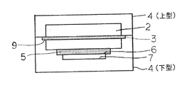
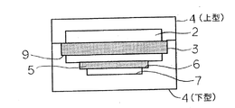
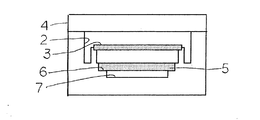
図3は本発明の金属−セラミックス基板を製造するための鋳型4であり上型、下型に分離できるようになっている。また、図3は鋳型4内にセラミックス基板5と強化材3であるセラミックス板材が設置された状態を示している。鋳型4の内部に金属ベース板1を形成するための金属ベース板1形成用の空洞部2が形成され、この空洞部2の側面の高さ方向(金属ベース板1の厚さ方向)の略中央部に強化材3である7個のセラミックス板材が空洞部2を横断してそれぞれの強化材3の一部(両端)が鋳型4の支持部9で挟持されるように形成され、さらに前記空洞部2の底面にセラミックス基板5を収容するための凹部6(ただし、図3はセラミックス基板5がすでに収容されている)が形成され、凹部6の底面に回路パターンである金属板8を形成するための凹部7(回路パターン用金属板形成用空洞部)が形成されたカーボン製の鋳型4を用意した。
なお、前記強化材3を挟持する支持部9は、金属ベース板1を形成するための空洞部2の側面(金属ベース板1の厚さ方向)の中央部に強化材3が挟持される構造、具体的には強化材3の断面の形状に略対応する穴がこの空洞部2の側面に形成されてたものであり、強化材3の数に応じて穴状の支持部9が形成されている。図3の場合は、金属ベース板1の幅方向及び厚さ方向の中央に1個の強化材3が鋳型4内に設置されるための挟持部9と、その両側に等間隔で支持部9が3個ずつ略平行に並んだものとなっている。
また、この強化材3を挟持する支持部9は鋳型4の上型鋳型と下型鋳型により形成されるようになっており、これにより、強化材3を下型の支持部9に設置した(置いた)後、上型を下型にのせることにより、強化材3が前記空洞部2を横断した状態に、所定の位置に精度良く設置(固定)することができる。なお、支持部9は上型、下型のいずれに設けてもかまわず、両方に設けてもかまわないし、適当な支持部材で形成しても良い。
また、この鋳型には、溶湯を鋳型4内に注湯するための注湯口(図示しない)が形成されているとともに、空洞部2(金属ベース板形成部)と凹部7(回路パターン用金属板形成部)との間に延びる溶湯流路(図示しない)が形成され、凹部6にセラミックス基板5を収容したときにも空洞部2(金属ベース板形成部)と凹部7(回路パターン用金属板形成部)との間が連通するようになっている。
(First embodiment)
A first embodiment will be described with reference to FIGS. 1, 2, and 3. FIG.
FIG. 3 shows a
In addition, the
Further, the
The mold has a pouring port (not shown) for pouring molten metal into the
この鋳型4の凹部6(セラミックス基板5収容部)内にセラミックス基板5を収容し、前記強化材3の支持部9に7本の強化材3を設置した後、前記鋳型4を接合炉(図示しない)内に移動させ、この炉内を窒素雰囲気にして酸素濃度を100ppm以下、好ましくは10ppm以下まで低下させ、ヒーターの温度制御によって鋳型4を注湯温度である例えば600〜800℃まで加熱した。
また、例えばアルミニウムである金属溶湯を、注湯温度まで加熱して得られた予め計量された金属溶湯を、狭隘部を有するノズル(図示しない)を通して酸化皮膜を取り除きながら、窒素ガスによって10kPaの圧力で加圧して、上記注湯口より加熱した鋳型内に流し込んだ。酸化皮膜を除去しながら注湯する、いわゆる溶湯接合以外の方法では、金属とセラミックスとの間で大きな接合欠陥が発生するおそれがある。
このようにして金属溶湯を流し込んだ後、ガス加圧ノズル(図示しない)から注湯口に窒素ガスを吹き込むことによって、鋳型4内のアルミニウム合金溶湯を10kPaの圧力で加圧したまま冷却して凝固させることが好ましい。
なお、ガスの注湯時や加圧時の圧力は1〜100kPaであるのが好ましく、3〜80kPaがさらに好ましく、5〜30kPaであることが最も好ましい。圧力が低すぎると金属溶湯が鋳型内に入りづらくなり、高すぎると強化材の位置がずれるおそれがあり、また鋳型が破壊される恐れがある。特に1MPa以上の高圧な場合は、カーボン製の鋳型4が破壊したり、強化材3やセラミックス基板5が、鋳型4内の所定位置からずれる恐れがある。
The
Further, for example, the pressure of 10 kPa is applied by nitrogen gas while removing the oxide film through a nozzle (not shown) having a narrow portion of a previously measured metal melt obtained by heating a metal melt of aluminum, for example, to a pouring temperature. And was poured into the heated mold from the pouring spout. In a method other than so-called melt bonding, in which the molten metal is poured while removing the oxide film, there is a possibility that a large bonding defect occurs between the metal and the ceramic.
After pouring the molten metal in this way, nitrogen gas is blown into the pouring port from a gas pressurizing nozzle (not shown) to cool and solidify the molten aluminum alloy in the
The pressure at the time of pouring or pressurizing the gas is preferably 1 to 100 kPa, more preferably 3 to 80 kPa, and most preferably 5 to 30 kPa. If the pressure is too low, it is difficult for the molten metal to enter the mold, and if it is too high, the position of the reinforcing material may be shifted, and the mold may be destroyed. In particular, when the pressure is 1 MPa or higher, the
このようにして、セラミックス基板の一方の面に金属板の一方の面が接合し、前記セラミックス基板の他方の面に金属ベース板の一方の面が接合した金属−セラミックス接合体を製造した。また、この金属ベース板の内部には7個の強化材3が貫通した状態となっている。なお、強化材3は1個でも良いし、複数の適当な個数でもよく、それは鋳型4の支持部9などを変更するなどによって対応できる。
この金属−セラミックス接合基板を鋳型から取り出し、金属ベース板1から飛び出した部分の強化材3(セラミックス板材)を除去した。強化材3の一部(端部)の除去は、既知の切断、ブレークなどで行えば良い。このようにして、本発明の金属−セラミックス接合基板を作製した。鋳型で強化材を支持することにより,金属ベース板1内の強化材3の位置(面方向の位置,厚さ方向の位置)を精密に制御、固定できるようになり,反りばらつきを抑制する制御ができるようになった。
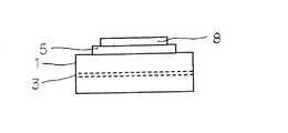
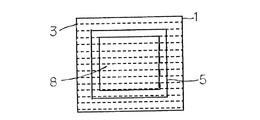
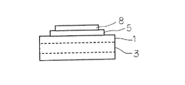
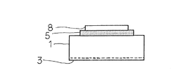
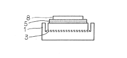
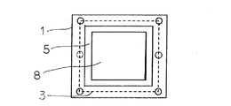
図1は本発明の金属−セラミックス接合基板の中央部の断面図、図2は上面図である。なおセラミックス基板5は複数であっても良い。図4は本発明の比較例1に対応する金属−セラミックス接合基板の模式断面図、図5は本発明の比較例1に対応する金属−セラミックス接合基板の模式平面図、図6は本発明の比較例1に対応する金属−セラミックス接合基板のための鋳型の模式断面図である。
In this way, a metal-ceramic bonding body was produced in which one surface of the metal plate was bonded to one surface of the ceramic substrate, and one surface of the metal base plate was bonded to the other surface of the ceramic substrate. In addition, seven reinforcing
The metal-ceramic bonding substrate was taken out from the mold, and the reinforcing material 3 (ceramic plate material) at the portion protruding from the
FIG. 1 is a sectional view of a central portion of a metal / ceramic bonding substrate of the present invention, and FIG. 2 is a top view. A plurality of
(第2の実施の形態)
第2の実施の形態について、図7、図8、図9を用いて説明する。
第1の実施の形態とほぼ同じで、強化材3も同様のセラミックス板材であるが、セラミックス板材が立てた状態(厚さ方向である側面が底面となる)である点のみが異なる。
セラミックス板材のサイズにもよるが、一般に厚さは幅に比べて小さいため、第1の実施の形態と同体積のセラミックス板材であれば、より厚さ方向の放熱に対し特に優れ、反りの抑制にもより優れる。すなわち金属−セラミックス接合基板の構造からも明らかなとおり、第1の実施の形態と比較して、厚さ方向に放熱をさえぎる強化材3の面積がより小さいことからあきらかで、また金属ベース板1の反りに対し強化材3が曲がりにくいことは厚さ方向の強化材3の寸法が大きいことからあきらかである。さらに強化材3の使用量を減らせるので、コストにも優れる。
(Second Embodiment)
A second embodiment will be described with reference to FIGS. 7, 8, and 9. FIG.
It is substantially the same as the first embodiment, and the reinforcing
Although it depends on the size of the ceramic plate, the thickness is generally smaller than the width. Therefore, if the ceramic plate has the same volume as the first embodiment, it is particularly excellent for heat dissipation in the thickness direction and suppresses warpage. Even better. That is, as apparent from the structure of the metal / ceramic bonding substrate, the area of the reinforcing
(第3の実施の形態)
第3の実施の形態について、図10、図11、図12を用いて説明する。
内部に金属ベース板1を形成するための空洞部2(金属ベース板形成部)が形成され、強化材3であるセラミックス板材を6本挟持する支持部9を有し、且つ図12に示すように該セラミックス板材3本が間隔をあけて配置され、残りの3本が前記3本の強化材3について、垂直(直角)な方向に間隔をあけて配置され挟持される支持部9を有するカーボン製の鋳型を用意した以外は第1の実施の形態と同じものである。
図10と図11に示す第3の実施の形態の金属−セラミックス接合基板の構造の通り、金属ベース板1の長さ方向に平行な方向(金属ベース板1の一辺に平行な方向、図11の左右方向)および幅方向(金属ベース板1の前記一辺に垂直な方向、図11の上下方向)に平行な方向のいずれにも方向にもセラミックス板材の強化材3が平行方向に接合されている。よって、金属ベース板の長さ方向に平行な方向と幅方向に平行な方向の両方向について反りを抑制する効果がある。
(Third embodiment)
A third embodiment will be described with reference to FIGS. 10, 11, and 12. FIG.
A hollow portion 2 (metal base plate forming portion) for forming the
As shown in the structure of the metal / ceramic bonding substrate of the third embodiment shown in FIGS. 10 and 11, the direction parallel to the length direction of the metal base plate 1 (the direction parallel to one side of the
(第4の実施の形態)
第4の実施の形態について、図13、図14、図15を用いて説明する。
強化材3のセラミックス板材が金属ベース板の他方の面(底面)に接合していること、強化材3が1個であること以外は、第1の実施の形態と同様の方法で、図13、図14に示す金属−セラミックス接合基板を作成することができる。鋳型4もそれに対応した図15に示すものとなる。
(Fourth embodiment)
A fourth embodiment will be described with reference to FIGS. 13, 14, and 15. FIG.
13 except that the ceramic plate material of the reinforcing
(第5の実施の形態)
第5の実施の形態について、図16、図17、図18を用いて説明する。
強化材3のセラミックス板材が金属ベース板1を形成する空洞2に、図18に示されるように第1の実施の形態と同様に強化材3が7個平行に設置されているのに加え、前記強化材3の長手方向と直角方向で且つ金属ベース板1の底面に近い方に1個の強化材3が鋳型4に設置されている以外は、第1の実施の形態と同様の方法で、図16、図17に示す金属−セラミックス接合基板を作成することができる。鋳型4もそれに対応した図18に示すものとなる。
(Fifth embodiment)
A fifth embodiment will be described with reference to FIGS. 16, 17, and 18. FIG.
In addition to the seven reinforcing
(第6の実施の形態)
第6の実施の形態について、図19、図20.図21を用いて説明する。
強化材3のセラミックス板材が金属ベース板1の周囲に、図21に示されるようにセラミックス板材を立てた状態で金属ベース板1の周囲に設置した以外は、第2の実施の形態と同様の方法で、図19、図20に示す金属−セラミックス接合基板を作成することができる。鋳型4もそれに対応した図21に示すものとなる。なお支持部9は図示していない。
(Sixth embodiment)
The sixth embodiment will be described with reference to FIGS. This will be described with reference to FIG.
The ceramic plate material of the reinforcing
(第7の実施の形態)
第7の実施の形態について、図22、図23、図24を用いて説明する。
強化材3のセラミックス板材が金属ベース板1の内部に、図24に示されるように1個のセラミックス板材を鋳型4で支持して配置する以外は、第1の実施の形態と同様の方法で、図22、図23に示す金属−セラミックス接合基板を作成することができる。鋳型4もそれに対応した図24に示すものとなる。
(Seventh embodiment)
A seventh embodiment will be described with reference to FIGS. 22, 23, and 24. FIG.
Except that the ceramic plate material of the reinforcing
ここで、本発明の金属−セラミックス基板は、セラミックス基板5の一方の面に金属板8の一方の面が接合するとともに、前記セラミックス基板5の他方の面に金属ベース板1の一方の面が接合した金属−セラミックス接合基板において、前記金属ベース板1に少なくとも1個以上の強化材3が接合され、且つ前記強化材の一部が前記金属ベース板1から露出している金属−セラミックス接合基板である。
前述の通り、本発明の鋳型で強化材3を支持することにより,作製された金属−セラミックス接合基板の金属ベース板1の一部に強化材3が露出した状態となる。また、金属ベース板3内の強化材3の位置(面方向の位置,厚さ方向の位置)を精密に制御できるようになり,反り制御ができるようになった。強化材3の接合や位置のよって放熱性が妨げられるが,本発明は強化材の配置、位置を精密に制御することによって反りの制御と放熱性確保の両立が得られた。
Here, in the metal-ceramic substrate of the present invention, one surface of the
As described above, by supporting the reinforcing
また、前記強化材の一部を鋳型に支持されるように設置した後、金属溶湯を注入して冷却凝固する方法、いわゆる溶湯接合法で金属−セラミックス接合基板を製造するのがよい。溶湯接合法によると、比較的低圧で注湯でき金属溶湯と強化材(例えばセラミックス板材や棒材)とがほとんど接合欠陥なしに接合することができ、金属溶湯は低圧なので前記強化材の初期の配置がずれる恐れがない。 In addition, it is preferable to manufacture a metal / ceramic bonding substrate by a method in which a part of the reinforcing material is installed so as to be supported by a mold and then a molten metal is injected and cooled and solidified, that is, a so-called molten bonding method. According to the molten metal joining method, the molten metal can be poured at a relatively low pressure, and the molten metal and the reinforcing material (for example, a ceramic plate or bar) can be joined with almost no joint defects. There is no risk of dislocation.
また、前記金属ベース板の一方の面から厚さ方向に垂直に透過してみたときの前記金属ベース板の一方の面の面積における前記強化材の占める部分の面積が、前記金属ベース板の一方の面の面積よりも小さいことが好ましく、前記セラミックス基板の一方の面から厚さ方向に垂直に透過してみたときの前記セラミックス基板の一方の面の面積における前記強化材の占める部分の面積が、前記セラミックス基板の一方の面の面積よりも小さいことが好ましい。 The area occupied by the reinforcing material in the area of one surface of the metal base plate when viewed perpendicularly in the thickness direction from one surface of the metal base plate is one of the metal base plates. Preferably, the area occupied by the reinforcing material in the area of one surface of the ceramic substrate when viewed perpendicularly in the thickness direction from one surface of the ceramic substrate is preferably smaller than the area of the surface of the ceramic substrate. The area of one surface of the ceramic substrate is preferably smaller.
回路用金属板上にはパワー素子などが搭載され、その素子の発熱による熱が下方の絶縁性のセラミックス基板(アルミナ基板、窒化アルミニウム基板、窒化珪素基板など)、金属ベース板に伝導させ、放熱する。
金属−セラミックス接合基板においては、金属とセラミックスとの熱膨張係数の違いにより接合時、あるいは金属−セラミックス接合基板にパワー素子などを搭載する熱処理時、実使用時などにおいて熱応力が発生し、金属−セラミックス基板が大きく反る。この反りを抑制するために、強化材として、例えばセラミックス基板に熱膨張係数が近いセラミックスや低熱膨張金属(Moなど)を金属ベース板中に接合する。
しかしながら、強化材は金属ベース板より熱伝導率が小さいことがほとんどで、また熱伝導率が同等以上の強化材(例えば高純度窒化アルミニウム基板)などは非常に高価でありパワーモジュールなどに使用するにはコストが全く適合しない。
本発明は前記金属ベースの一方の面から厚さ方向に垂直に透過してみたときの前記金属ベース板の一方の面の面積における前記強化材の占める部分の面積が、前記金属ベース板の一方の面の面積よりも小さくし、前記セラミックス基板の一方の面から厚さ方向に垂直に透過してみたときの前記セラミックス基板の一方の面の面積における前記強化材の占める部分の面積が、前記セラミックス基板の一方の面の面積よりも小さくするように強化材を配置し接合することにより、すなわち特に板材や棒材の金属ベース板への接合する位置や大きさを正確、精密にすることで、強化材が熱伝導に劣るものでも、熱伝導率をほぼ低下させることなく且つ反りが充分に少ない金属−セラミックス接合基板を提供できる。
A power element or the like is mounted on the circuit metal plate, and the heat generated by the element is conducted to the insulating ceramic substrate (alumina substrate, aluminum nitride substrate, silicon nitride substrate, etc.) and the metal base plate below to dissipate heat. To do.
In metal-ceramic bonding substrates, thermal stress occurs during bonding, due to the difference in thermal expansion coefficient between metal and ceramics, during heat treatment for mounting power elements etc. on metal-ceramic bonding substrates, and during actual use. -The ceramic substrate warps greatly. In order to suppress this warpage, as a reinforcing material, for example, a ceramic or a low thermal expansion metal (such as Mo) having a thermal expansion coefficient close to that of the ceramic substrate is bonded to the metal base plate.
However, most of the reinforcing materials have a lower thermal conductivity than the metal base plate, and reinforcing materials (for example, high-purity aluminum nitride substrates) having the same or higher thermal conductivity are very expensive and used for power modules and the like. The cost does not fit at all.
In the present invention, the area occupied by the reinforcing material in the area of one surface of the metal base plate when viewed perpendicularly in the thickness direction from one surface of the metal base is one of the metal base plates. The area occupied by the reinforcing material in the area of one surface of the ceramic substrate when viewed perpendicularly in the thickness direction from one surface of the ceramic substrate is smaller than the area of the surface of the ceramic substrate, By arranging and joining reinforcing materials so that they are smaller than the area of one side of the ceramic substrate, that is, by accurately and precisely adjusting the position and size of the plates and bars to the metal base plate Even if the reinforcing material is inferior in heat conduction, it is possible to provide a metal / ceramic bonding substrate with substantially no warpage and substantially no reduction in heat conductivity.
また、前記強化材が複数個あり、それぞれの前記強化材の一部が前記金属ベース板から露出していることが好ましく、前記強化材が板状または棒状であることが好ましく、前記強化材が複数個あり、前記金属ベース板の一方の面から厚さ方向に垂直に透過して見たとき、前記強化材が格子状をなしていることが好ましい。 Moreover, it is preferable that there are a plurality of the reinforcing materials, and that a part of each of the reinforcing materials is exposed from the metal base plate, the reinforcing material is preferably plate-shaped or rod-shaped, and the reinforcing material is It is preferable that the reinforcing material has a lattice shape when viewed through one surface of the metal base plate perpendicularly in the thickness direction.
さらに、前記金属ベース板がアルミニウムまたはアルミニウム合金であることが電気伝導性、熱伝導率、セラミックス基板との接合の信頼性の観点で好ましく、前記強化材の材質がセラミックスであることが好ましく、前記強化材の材質がアルミナ、窒化アルミニウム、窒化珪素、炭化珪素から選ばれる少なくとも1つの原料からなるセラミックスであることが好ましく、前記金属板が電気伝導性、熱伝導率、セラミックス基板との接合の信頼性の観点でアルミニウムまたはアルミニウム合金であることが好ましい。 Further, the metal base plate is preferably aluminum or an aluminum alloy from the viewpoint of electrical conductivity, thermal conductivity, and reliability of bonding with a ceramic substrate, and the material of the reinforcing material is preferably ceramic, The reinforcing material is preferably a ceramic made of at least one raw material selected from alumina, aluminum nitride, silicon nitride, and silicon carbide, and the metal plate has electrical conductivity, thermal conductivity, and reliability of bonding with the ceramic substrate. From the viewpoint of safety, aluminum or an aluminum alloy is preferable.
さらに、前記セラミックス基板がアルミナ、窒化アルミニウム、窒化珪素、炭化珪素から選ばれる少なくとも1つの原料からなるセラミックスであることが好ましく、前記強化材が複数個あり、それらが略同一平面上に接合されていることが設置のしやすさのため好ましく、前記強化材が複数個あり、それらが略平行に接合されているのが好ましい。 Furthermore, the ceramic substrate is preferably a ceramic made of at least one raw material selected from alumina, aluminum nitride, silicon nitride, and silicon carbide. There are a plurality of the reinforcing materials, and they are bonded on substantially the same plane. It is preferable for ease of installation, and there are a plurality of the reinforcing materials, and it is preferable that they are joined substantially in parallel.
なお、本発明は前記実施の形態のみにとらわれるものではない。 The present invention is not limited to the above embodiment.
以下、本発明による金属−セラミックス接合基板の製造方法の実施例について詳細に説明する。 Examples of the method for producing a metal / ceramic bonding substrate according to the present invention will be described in detail below.
[実施例1]
(図1〜3参照)
まず、内部に70mm×70mm×5mmの大きさのベース板を形成するための空洞部(金属ベース板形成部)が形成され、この空洞部の側面の高さ方向(金属ベース板の厚さ方向)の中央部に80mm×5mm×0.6mmの強化材であるセラミックス板材7本が空洞部を横断してそれぞれのセラミックス板材の両端5mmが鋳型で狭持されるように形成され、さらに前記空洞部の底面に50mm×50mm×0.6mmの大きさのセラミックス基板を収容するための凹部(セラミックス基板収容部)が形成され、これらの凹部の底面に48mm×48mm×0.6mmの大きさの回路パターン用金属板を形成するための凹部(回路パターン用金属板形成部)が形成されたカーボン製の鋳型を用意した。なお、前記セラミックス板材の狭持部は、ベース板を形成するための空間の横方向(ベース板の幅方向)の中心に1本狭持される構造、すなわち略5mm幅で高さ略0.6mm、深さ略5mmの穴がこの空間部の側面に形成されており、この中心の1本から隙間5mmを空けて等間隔に略並行に、且つ同一平面状に挟持する同様の穴が形成されている。また、このセラミックス板材を挟持する穴は、鋳型が上型と下型に分離できるようになっており、上型と下型を組み合わせることで形成される。セラミックス板材をこの穴に入れて前記空間を横断した状態とすることができる。
また、この鋳型には、溶湯を鋳型内に注湯するための注湯口が形成されているとともに、金属ベース板形成部と回路パターン用金属板形成部との間に延びる溶湯流路が形成され、セラミックス基板収容部内にセラミックス基板を収容したときにもベース板形成部と回路パターン用金属板形成部との間が連通するようになっている。
[Example 1]
(See Figures 1-3)
First, a hollow portion (metal base plate forming portion) for forming a base plate having a size of 70 mm × 70 mm × 5 mm is formed inside, and the height direction of the side surface of this hollow portion (thickness direction of the metal base plate) 7) are formed so that seven ceramic plate members, which are 80 mm × 5 mm × 0.6 mm reinforcing materials, cross the cavity and 5 mm on both ends of each ceramic plate are sandwiched between molds. Recesses (ceramic substrate accommodation portions) for accommodating ceramic substrates having a size of 50 mm × 50 mm × 0.6 mm are formed on the bottom surfaces of the portions, and the bottom surfaces of these recesses have a size of 48 mm × 48 mm × 0.6 mm. A carbon mold having a recess (circuit pattern metal plate forming portion) for forming a circuit pattern metal plate was prepared. In addition, the sandwiching portion of the ceramic plate material is structured such that one is sandwiched in the center in the lateral direction of the space for forming the base plate (the width direction of the base plate), that is, approximately 5 mm wide and approximately 0. A hole of 6 mm and a depth of about 5 mm is formed in the side surface of this space portion, and a similar hole is formed that is sandwiched in the same plane with a gap of 5 mm from one of the centers, at approximately equal intervals. Has been. Further, the hole for sandwiching the ceramic plate material is configured such that the mold can be separated into an upper mold and a lower mold, and is formed by combining the upper mold and the lower mold. A ceramic plate material can be put in this hole to cross the space.
The mold has a pouring port for pouring the molten metal into the mold, and a molten metal flow path extending between the metal base plate forming portion and the circuit pattern metal plate forming portion. Even when the ceramic substrate is accommodated in the ceramic substrate accommodating portion, the base plate forming portion and the circuit pattern metal plate forming portion communicate with each other.
この鋳型のセラミックス基板収容部内に50mm×50mm×0.6mmの大きさの窒化アルミニウム基板を収容し、前記セラミックス板材の収容部(穴)に80mm×5mm×0.6mmの窒化アルミニウム板材7本を炉内に入れ、この炉内を窒素雰囲気にして酸素濃度を4ppmまで低下させ、ヒーターの温度制御によって鋳型を730℃まで加熱した。 An aluminum nitride substrate having a size of 50 mm × 50 mm × 0.6 mm is accommodated in the ceramic substrate accommodating portion of this mold, and seven 80 mm × 5 mm × 0.6 mm aluminum nitride plates are accommodated in the ceramic plate accommodating portion (hole). The furnace was placed in a furnace, the inside of the furnace was placed in a nitrogen atmosphere, the oxygen concentration was lowered to 4 ppm, and the mold was heated to 730 ° C. by controlling the temperature of the heater.
また、アルミニウムを740℃まで加熱して得られた予め計量されたアルミニウム合金溶湯を、狭隘部を有するノズルを通して酸化皮膜を取り除きながら、窒素ガスによって10kPaの圧力で加圧して、上記注湯口より加熱した鋳型内に流し込んだ。 Further, a pre-weighed aluminum alloy melt obtained by heating aluminum to 740 ° C. is pressurized with nitrogen gas at a pressure of 10 kPa while removing the oxide film through a nozzle having a narrow portion, and heated from the pouring port. Poured into the mold.
このようにしてアルミニウム溶湯を流し込んだ後、ガス加圧ノズルから注湯口に窒素ガスを吹き込むことによって、鋳型内のアルミニウム合金溶湯を10kPaの圧力で加圧したまま冷却して凝固させた。 After pouring the molten aluminum in this way, nitrogen gas was blown into the pouring port from the gas pressurizing nozzle, whereby the molten aluminum alloy in the mold was cooled and solidified while being pressurized at a pressure of 10 kPa.
このようにして、70mm×70mm×5mmの大きさのアルミニウムからなる金属ベース板上に、50mm×50mm×0.6mmの大きさの窒化アルミニウム基板が接合し、これらの窒化アルミニウム基板上にそれぞれ48mm×48mm×0.6mmの大きさの回路パターン用アルミニウム金属板が接合した金属−セラミックス接合体を製造した。また、この金属ベース板の内部には80mm×5mm×0.6mmのセラミックス板材7本が貫通した状態となっている。 In this way, an aluminum nitride substrate having a size of 50 mm × 50 mm × 0.6 mm is bonded onto a metal base plate made of aluminum having a size of 70 mm × 70 mm × 5 mm, and each of these aluminum nitride substrates has a thickness of 48 mm. A metal-ceramic bonded body in which an aluminum metal plate for circuit pattern having a size of × 48 mm × 0.6 mm was bonded was manufactured. In addition, seven 80 mm × 5 mm × 0.6 mm ceramic plate materials penetrate through the metal base plate.
この金属−セラミックス接合基板を鋳型から取り出し、金属ベース板から飛び出した部分のセラミックス板材を切断除去した。このようにして、アルミニウムベース板上にセラミックス基板が接合し、その上にアルミニウム回路板が接合した金属−セラミックス接合基板を作製した。 The metal-ceramic bonding substrate was taken out from the mold, and the ceramic plate material of the portion protruding from the metal base plate was cut and removed. In this manner, a metal / ceramic bonding substrate in which a ceramic substrate was bonded onto an aluminum base plate and an aluminum circuit plate was bonded thereon was produced.
この金属−セラミックス接合基板の回路用金属板の表面の反り量を、金属板の中央部をセラミックス板材の長手と平行方向、直角方向についてスパン45mmとしてレーザー変位計で測定し、下側に反ったもの(凹状)を正(+)とし、上側に反ったもの(凸状)を負(−)とした。
セラミックス板材の長手と平行方向のときの反り量は−36μm、直角方向のときの反り量は−198μmであった。
The amount of warpage of the surface of the metal plate for circuit of this metal-ceramic bonding substrate was measured with a laser displacement meter with the central portion of the metal plate being parallel to the longitudinal direction of the ceramic plate material and a span of 45 mm in the perpendicular direction, and warped downward. The thing (concave shape) was positive (+), and the one warped upward (convex shape) was negative (-).
The amount of warpage when the ceramic plate was parallel to the longitudinal direction was −36 μm, and the amount of warpage when the ceramic plate was perpendicular was −198 μm.
さらに410℃×10分を1回とする通炉試験を1回、3回、5回、10回としたときの反り量を測定した。
通炉が1回終わったとき、セラミックス板材の長手と平行方向のときの反り量は−33μm、直角方向のときの反り量は−264μmであった。
通炉が3回終わったとき、セラミックス板材の長手と平行方向のときの反り量は−57μm、直角方向のときの反り量は−309μmであった。
通炉が5回終わったとき、セラミックス板材の長手と平行方向のときの反り量は−69μm、直角方向のときの反り量は−342μmであった。
通炉が10回終わったとき、セラミックス板材の長手と平行方向のときの反り量は−90μm、直角方向のときの反り量は−390μmであった。
Furthermore, the amount of warpage was measured when the furnace test with 410 ° C. × 10 minutes once was performed once, three times, five times, and ten times.
When the furnace passed once, the warpage amount in the direction parallel to the longitudinal direction of the ceramic plate was −33 μm, and the warpage amount in the perpendicular direction was −264 μm.
When the furnace passed three times, the warpage amount in the direction parallel to the length of the ceramic plate was −57 μm, and the warpage amount in the perpendicular direction was −309 μm.
When the furnace passed five times, the warpage amount in the direction parallel to the longitudinal direction of the ceramic plate was −69 μm, and the warpage amount in the perpendicular direction was −342 μm.
When the furnace passed 10 times, the warpage amount in the direction parallel to the longitudinal direction of the ceramic plate was −90 μm, and the warpage amount in the perpendicular direction was −390 μm.
また、通炉試験後もセラミックス基板の割れなどの不具合はなく、絶縁性などの電気性能も良好であった。金属板とセラミックス基板、金属ベース板とセラミックス基板、金属ベース板とセラミックス板材のそれぞれの接合も特に欠陥はなく良好であった。 Moreover, after the furnace test, there were no problems such as cracking of the ceramic substrate, and the electrical performance such as insulation was good. The bonding of the metal plate and the ceramic substrate, the metal base plate and the ceramic substrate, and the metal base plate and the ceramic plate material was also good with no defects.
[実施例2]
前記金属ベース板用の空洞部の側面の高さ方向(金属ベース板の厚さ方向)と幅方向の中央部に80mm×50mm×0.6mmの強化材であるセラミックス板材1本が、空洞部を横断してセラミックス板材の両端5mmが鋳型で狭持されるように形成されたカーボン製の鋳型を用意し、すなわち略50mm幅で高さ略0.6mm、深さ略5mmの穴がこの空間部の側面に形成した以外は実施例1と同様の方法で金属−セラミックス接合基板を作成した。
この金属−セラミックス接合基板の回路用金属板の表面の反り量を、実施例1と同様に測定したところ、セラミックス板材の長手と平行方向のときの反り量は−36μm、直角方向のときの反り量は−45μmであった。
さらに実施例1と同様の通炉試験を1回、3回、5回、10回としたときの反り量を測定した。
通炉が1回終わったとき、セラミックス板材の長手と平行方向のときの反り量は−42μm、直角方向のときの反り量は−42μmであった。
通炉が3回終わったとき、セラミックス板材の長手と平行方向のときの反り量は−18μm、直角方向のときの反り量は−18μmであった。
通炉が5回終わったとき、セラミックス板材の長手と平行方向のときの反り量は−30μm、直角方向のときの反り量は−27μmであった。
通炉が10回終わったとき、セラミックス板材の長手と平行方向のときの反り量は−63μm、直角方向のときの反り量は−63μmであった。
[Example 2]
A ceramic plate material, which is a reinforcing material of 80 mm × 50 mm × 0.6 mm, is provided at the center in the height direction (thickness direction of the metal base plate) and the width direction of the side surface of the cavity for the metal base plate. A carbon mold is prepared so that both ends of the ceramic plate material are sandwiched between the molds, that is, a hole having a width of about 50 mm, a height of about 0.6 mm, and a depth of about 5 mm. A metal / ceramic bonding substrate was prepared in the same manner as in Example 1 except that the metal-ceramic bonding substrate was formed on the side surface of the part.
The amount of warpage of the surface of the metal plate for circuit of this metal-ceramic bonding substrate was measured in the same manner as in Example 1. As a result, the amount of warpage in the direction parallel to the longitudinal direction of the ceramic plate was -36 μm, and the amount of warpage in the right-angle direction. The amount was -45 μm.
Further, the amount of warpage was measured when the furnace test similar to that in Example 1 was performed once, three times, five times, and ten times.
When the furnace passed once, the warpage amount in the direction parallel to the longitudinal direction of the ceramic plate was −42 μm, and the warpage amount in the perpendicular direction was −42 μm.
When the furnace passed three times, the warpage amount in the direction parallel to the longitudinal direction of the ceramic plate material was -18 μm, and the warpage amount in the right-angle direction was −18 μm.
When the furnace passed five times, the warpage amount in the direction parallel to the longitudinal direction of the ceramic plate was −30 μm, and the warpage amount in the perpendicular direction was −27 μm.
When the furnace passed 10 times, the warpage amount in the direction parallel to the longitudinal direction of the ceramic plate was −63 μm, and the warpage amount in the perpendicular direction was −63 μm.
[比較例1]
(図4〜6参照)
前記金属ベース板用の空洞部に強化材であるセラミックス板材を挟持される穴を前記鋳型に設けておらず、セラミックス板材の強化材を接合しなかった以外は実施例1と同様の方法で金属−セラミックス接合基板を作成した。
この金属−セラミックス接合基板の回路用金属板の表面の反り量を、実施例1と同様に測定したところ、セラミックス板材の長手と平行方向のときの反り量は−231μm、直角方向のときの反り量は−201μmであった。
さらに実施例1と同様の通炉試験を1回、3回、5回、10回としたときの反り量を測定した。
通炉が1回終わったとき、セラミックス板材の長手と平行方向のときの反り量は−273μm、直角方向のときの反り量は−252μmであった。
通炉が3回終わったとき、セラミックス板材の長手と平行方向のときの反り量は−321μm、直角方向のときの反り量は−294μmであった。
通炉が5回終わったとき、セラミックス板材の長手と平行方向のときの反り量は−351μm、直角方向のときの反り量は−333μmであった。
通炉が10回終わったとき、セラミックス板材の長手と平行方向のときの反り量は−399μm、直角方向のときの反り量は−393μmであった。
[Comparative Example 1]
(See Figures 4-6)
The metal base plate was made of a metal in the same manner as in Example 1 except that the cavity for sandwiching the ceramic plate material as a reinforcing material was not provided in the mold and the ceramic plate reinforcing material was not joined. -A ceramic bonded substrate was prepared.
The amount of warpage of the surface of the metal plate for circuit of this metal-ceramic bonding substrate was measured in the same manner as in Example 1. As a result, the amount of warpage in the direction parallel to the longitudinal direction of the ceramic plate was -231 μm, and the amount of warpage in the perpendicular direction. The amount was -201 μm.
Further, the amount of warpage was measured when the furnace test similar to that in Example 1 was performed once, three times, five times, and ten times.
When the furnace passed once, the warpage amount in the direction parallel to the longitudinal direction of the ceramic plate material was −273 μm, and the warpage amount in the perpendicular direction was −252 μm.
When the furnace passed three times, the warpage amount in the direction parallel to the length of the ceramic plate was −321 μm, and the warpage amount in the perpendicular direction was −294 μm.
When the furnace passed 5 times, the warpage amount in the direction parallel to the longitudinal direction of the ceramic plate was −351 μm, and the warpage amount in the perpendicular direction was −333 μm.
When the furnace passed 10 times, the warpage amount in the direction parallel to the longitudinal direction of the ceramic plate was -399 μm, and the warpage amount in the perpendicular direction was −393 μm.
[実施例3]
実施例1と同様の条件で金属−セラミックス接合基板を作製した。
この金属−セラミックス接合基板の回路用金属板の表面の反り量を、実施例1と同様に測定した結果、セラミックス板材の長手と平行方向のときの反り量は−45μm、直角方向のときの反り量は−201μmであった。
また、金属−セラミックス基板の金属ベース板の表面の反り量についても測定した。金属ベース板の中央部をセラミックス板材の長手と平行方向、直角方向についてスパン60mmとしてレーザー変位計で測定し、上側に反ったもの(凸状)を正(+)とし、下側に反ったもの(凹状)を負(−)とした。その結果、セラミックス板材の長手と平行方向のときの反り量は−84μm、直角方向のときの反り量は−336μmであった。
[Example 3]
A metal / ceramic bonding substrate was produced under the same conditions as in Example 1.
As a result of measuring the warpage amount of the surface of the metal plate for circuit of this metal-ceramic bonding substrate in the same manner as in Example 1, the warpage amount in the direction parallel to the longitudinal direction of the ceramic plate material was −45 μm, and the warpage in the perpendicular direction. The amount was -201 μm.
Further, the amount of warpage of the surface of the metal base plate of the metal-ceramic substrate was also measured. The center part of the metal base plate is measured with a laser displacement meter with a span of 60 mm in the direction parallel to the longitudinal direction of the ceramic plate material, and the direction perpendicular to it, and the one that warps upward (convex shape) is positive (+) and warps downward The (concave shape) was negative (-). As a result, the warpage amount in the direction parallel to the longitudinal direction of the ceramic plate was −84 μm, and the warpage amount in the perpendicular direction was −336 μm.
[実施例4]
金属ベース板を形成するための空洞部の側面に強化材であるセラミックス板材6本が空洞部を横断し、前記セラミックス板材の挟持部は、ベース板を形成するための空間の横方向(ベース板の幅方向)の端から2.5mmの距離のところに1本挟持され、すなわち略5mm幅で高さ略0.6mm、深さ略5mmの穴がこの空間部の側面に形成されており、この1本から5mm間隔で5本のセラミックス板材に対応する穴が略並行に形成され、且つ同一平面状に狭持する同様の穴が形成され、セラミックス板材を6本鋳型に設置し、金属ベース板に接合した以外は、実施例1と同様の条件で金属−セラミックス接合基板を作製した。
この金属−セラミックス接合基板の回路用金属板の表面の反り量を、実施例1と同様に測定した結果、セラミックス板材の長手と平行方向のときの反り量は−51μm、直角方向のときの反り量は−219μmであった。
また、金属−セラミックス基板の金属ベース板の表面の反り量についても実施例3と同様に測定した結果、セラミックス板材の長手と平行方向のときの反り量は−84μm、直角方向のときの反り量は−381μmであった。
[Example 4]
Six ceramic plate members, which are reinforcing materials, cross the cavity portion on the side surface of the cavity portion for forming the metal base plate, and the sandwiching portion of the ceramic plate material is a lateral direction of the space for forming the base plate (base plate One hole is sandwiched at a distance of 2.5 mm from the end of the width direction), that is, a hole having a width of about 5 mm, a height of about 0.6 mm, and a depth of about 5 mm is formed on the side surface of the space portion. Holes corresponding to five ceramic plates at intervals of 1 to 5 mm are formed substantially in parallel, and similar holes are formed so as to be held in the same plane. A metal / ceramic bonding substrate was produced under the same conditions as in Example 1 except that the substrate was bonded to the plate.
The amount of warpage of the surface of the metal plate for circuit of this metal-ceramic bonding substrate was measured in the same manner as in Example 1. As a result, the amount of warpage in the direction parallel to the longitudinal direction of the ceramic plate was -51 μm, and the amount of warpage in the perpendicular direction. The amount was -219 μm.
Further, the amount of warpage of the surface of the metal base plate of the metal-ceramic substrate was also measured in the same manner as in Example 3. As a result, the amount of warpage in the direction parallel to the longitudinal direction of the ceramic plate was -84 μm, and the amount of warpage in the right-angle direction. Was −381 μm.
[実施例5]
実施例3と同様に金属−セラミックス接合基板を作製した。
この金属−セラミックス接合基板の回路用金属板の表面の反り量を、実施例1と同様に測定した結果、セラミックス板材の長手と平行方向のときの反り量は−27μm、直角方向のときの反り量は−45μmであった。
また、金属−セラミックス基板の金属ベース板の表面の反り量についても実施例3と同様に測定した結果、セラミックス板材の長手と平行方向のときの反り量は−33μm、直角方向のときの反り量は−78μmであった。
[Example 5]
A metal / ceramic bonding substrate was prepared in the same manner as in Example 3.
The amount of warpage of the surface of the metal plate for circuit of this metal-ceramic bonding substrate was measured in the same manner as in Example 1. As a result, the amount of warpage in the direction parallel to the longitudinal direction of the ceramic plate was −27 μm, and the amount of warpage in the right-angle direction. The amount was -45 μm.
Further, the amount of warpage of the surface of the metal base plate of the metal-ceramic substrate was measured in the same manner as in Example 3. As a result, the amount of warpage in the direction parallel to the longitudinal direction of the ceramic plate was -33 μm, and the amount of warpage in the direction perpendicular to the ceramic plate. Was −78 μm.
[実施例6]
セラミックス板材が金属ベース板のセラミックス基板接合側と反対の表面に露出し、その表面と略同一平面に接合されるように、鋳型の挟持する穴を設けた以外は、実施例3と同様の方法で金属−セラミックス接合基板を作製した。
この金属−セラミックス接合基板の回路用金属板の表面の反り量を、実施例1と同様に測定した結果、セラミックス板材の長手と平行方向のときの反り量は−33μm、直角方向のときの反り量は−264μmであった。
また、金属−セラミックス基板の金属ベース板の表面の反り量についても実施例3と同様に測定した結果、セラミックス板材の長手と平行方向のときの反り量は−39μm、直角方向のときの反り量は−447μmであった。
[Example 6]
The same method as in Example 3 except that a hole for holding the mold is provided so that the ceramic plate material is exposed on the surface opposite to the ceramic substrate bonding side of the metal base plate and is bonded to the surface substantially in the same plane. A metal-ceramic bonding substrate was prepared.
The amount of warpage of the surface of the metal plate for circuit of this metal-ceramic bonding substrate was measured in the same manner as in Example 1. As a result, the amount of warpage in the direction parallel to the longitudinal direction of the ceramic plate was −33 μm, and the amount of warpage in the direction perpendicular to the ceramic plate. The amount was -264 μm.
Further, the amount of warpage of the surface of the metal base plate of the metal-ceramic substrate was also measured in the same manner as in Example 3. As a result, the amount of warpage in the direction parallel to the longitudinal direction of the ceramic plate was -39 μm, and the amount of warpage in the right-angle direction. Was −447 μm.
[実施例7]
前記金属ベース板用の空洞部の側面の高さ方向(金属ベース板の厚さ方向)と幅方向の中央部に80mm×60mm×0.6mmの強化材であるセラミックス板材1本が、空洞部を横断してセラミックス板材の両端5mmが鋳型で挟持されるように形成されたカーボン製の鋳型を用意し、すなわち略60mm幅で高さ略0.6mm、深さ略5mmの穴がこの空間部の側面に形成した以外は実施例1と同様の方法で金属−セラミックス接合基板を作成した。
この金属−セラミックス接合基板の回路用金属板の表面の反り量を、実施例1と同様に測定した結果、セラミックス板材の長手と平行方向のときの反り量は−21μm、直角方向のときの反り量は−21μmであった。
また、金属−セラミックス基板の金属ベース板の表面の反り量についても実施例3と同様に測定した結果、セラミックス板材の長手と平行方向のときの反り量は−30μm、直角方向のときの反り量は−39μmであった。
[Example 7]
One ceramic plate material, which is a reinforcing material of 80 mm × 60 mm × 0.6 mm, is provided at the center in the height direction (thickness direction of the metal base plate) and the width direction of the side surface of the cavity for the metal base plate. A carbon mold is prepared so that both ends of the ceramic plate are sandwiched between the molds, that is, a hole having a width of about 60 mm, a height of about 0.6 mm, and a depth of about 5 mm. A metal / ceramic bonding substrate was prepared in the same manner as in Example 1 except that it was formed on the side surface.
As a result of measuring the warpage amount of the metal plate for circuit of this metal-ceramic bonding substrate in the same manner as in Example 1, the warpage amount in the direction parallel to the longitudinal direction of the ceramic plate material was −21 μm, and the warpage in the right angle direction. The amount was -21 μm.
Further, the amount of warpage of the surface of the metal base plate of the metal-ceramic substrate was also measured in the same manner as in Example 3. As a result, the amount of warpage in the direction parallel to the longitudinal direction of the ceramic plate was -30 μm, and the amount of warpage in the direction perpendicular to the ceramic plate. Was −39 μm.
[実施例8]
(図13〜15参照)
セラミックス板材が金属ベース板のセラミックス基板接合側と反対の表面に露出し、その表面と略同一平面に接合されるように、鋳型の狭持する穴を設けた以外は、実施例7と同様の方法で金属−セラミックス接合基板を作製した。
この金属−セラミックス接合基板の回路用金属板の表面の反り量を、実施例1と同様に測定した結果、セラミックス板材の長手と平行方向のときの反り量は−45μm、直角方向のときの反り量は−15μmであった。
また、金属−セラミックス基板の金属ベース板の表面の反り量についても実施例3と同様に測定した結果、セラミックス板材の長手と平行方向のときの反り量は−72μm、直角方向のときの反り量は−42μmであった。
[Example 8]
(See Figs. 13-15)
The same as in Example 7 except that a hole for holding the mold is provided so that the ceramic plate material is exposed on the surface opposite to the ceramic substrate bonding side of the metal base plate and bonded to the surface substantially in the same plane. A metal-ceramic bonding substrate was produced by the method.
As a result of measuring the warpage amount of the surface of the metal plate for circuit of this metal-ceramic bonding substrate in the same manner as in Example 1, the warpage amount in the direction parallel to the longitudinal direction of the ceramic plate material was −45 μm, and the warpage in the perpendicular direction. The amount was −15 μm.
Further, the amount of warpage of the surface of the metal base plate of the metal-ceramic substrate was measured in the same manner as in Example 3. As a result, the amount of warpage in the direction parallel to the length of the ceramic plate was -72 μm, and the amount of warpage in the direction perpendicular to the ceramic plate. Was −42 μm.
[比較例2]
比較例1と同様に金属−セラミックス接合基板を作製した。
この金属−セラミックス接合基板の回路用金属板の表面の反り量を、実施例1と同様に測定した結果、セラミックス板材の長手と平行方向のときの反り量は−213μm、直角方向のときの反り量は−177μmであった。
また、金属−セラミックス基板の金属ベース板の表面の反り量についても実施例3と同様に測定した結果、セラミックス板材の長手と平行方向のときの反り量は−387μm、直角方向のときの反り量は−345μmであった。
[Comparative Example 2]
A metal / ceramic bonding substrate was prepared in the same manner as in Comparative Example 1.
As a result of measuring the warpage amount of the metal plate for circuit of this metal-ceramic bonding substrate in the same manner as in Example 1, the warpage amount in the direction parallel to the longitudinal direction of the ceramic plate material was −213 μm, and the warpage in the right angle direction. The amount was -177 μm.
Further, the amount of warpage of the surface of the metal base plate of the metal-ceramic substrate was also measured in the same manner as in Example 3. As a result, the amount of warpage in the direction parallel to the longitudinal direction of the ceramic plate was -387 μm, and the amount of warpage in the perpendicular direction. Was −345 μm.
[実施例9]
内部に70mm×70mm×4mmの大きさのベース板を形成するための空洞部(金属ベース板形成部)が形成され、この空洞部の側面の高さ方向(金属ベース板の厚さ方向)の中央部に80mm×10mm×0.6mmの強化材であるセラミックス板材3本が空洞部を横断してそれぞれのセラミックス板材の両端5mmが鋳型で狭持されるように形成されたカーボン製の鋳型を用意した以外は実施例1と同様に金属−セラミックス接合基板を作製した。
これにより70mm×70mm×4mmの大きさのアルミニウムからなる金属ベース板上に、50mm×50mm×0.6mmの大きさの窒化アルミニウム基板が接合し、これらの窒化アルミニウム基板上にそれぞれ48mm×48mm×0.4mmの大きさの回路パターン用アルミニウム金属板が接合した金属−セラミックス接合体が得られた。また、この金属ベース板の内部には強化材である80mm×10mm×0.6mmのセラミックス板材3本が形成されている。
また、金属−セラミックス基板の金属ベース板の表面の反り量についても実施例3と同様に測定した結果、セラミックス板材の長手と平行方向のときの反り量は−30μmであった。
[Example 9]
A hollow portion (metal base plate forming portion) for forming a base plate having a size of 70 mm × 70 mm × 4 mm is formed inside, and the height direction of the side surface of the hollow portion (thickness direction of the metal base plate) is formed. A carbon mold formed in such a manner that three ceramic plate members, which are 80 mm × 10 mm × 0.6 mm reinforcing materials, cross the hollow portion and 5 mm on both ends of each ceramic plate material is held between the molds in the center. A metal / ceramic bonding substrate was produced in the same manner as in Example 1 except that it was prepared.
As a result, an aluminum nitride substrate having a size of 50 mm × 50 mm × 0.6 mm is bonded onto a metal base plate made of aluminum having a size of 70 mm × 70 mm × 4 mm, and 48 mm × 48 mm × on each of these aluminum nitride substrates. A metal-ceramic bonding body in which an aluminum metal plate for circuit patterns having a size of 0.4 mm was bonded was obtained. In addition, three ceramic plate members of 80 mm × 10 mm × 0.6 mm, which are reinforcing materials, are formed inside the metal base plate.
Further, the amount of warpage of the surface of the metal base plate of the metal-ceramic substrate was also measured in the same manner as in Example 3. As a result, the amount of warpage in the direction parallel to the longitudinal direction of the ceramic plate material was −30 μm.
[実施例10]
金属ベース板を形成するための空洞部の側面の高さ方向(金属ベース板の厚さ方向)の中央部に80mm×3mm×0.6mmの強化材であるセラミックス板材3本が空洞部を横断してそれぞれのセラミックス板材の両端5mmが鋳型で挟持されるように形成され、前記セラミックス板材の挟持部は、ベース板を形成するための空間の横方向(ベース板の幅方向)の中心に1本挟持される構造、すなわち略0.6mm幅で高さ略3mm、深さ略5mmの穴がこの空間部の側面に形成されており、この中心の1本から20mm間隔に略並行に、且つ同一平面状に挟持する同様の穴が形成されたカーボン製の鋳型を用意した以外は実施例1と同様に金属−セラミックス接合基板を作製した。
これにより70mm×70mm×4mmの大きさのアルミニウムからなる金属ベース板上に、50mm×50mm×0.6mmの大きさの窒化アルミニウム基板が接合し、これらの窒化アルミニウム基板上にそれぞれ48mm×48mm×0.4mmの大きさの回路パターン用アルミニウム金属板が接合した金属−セラミックス接合体が得られた。また、この金属ベース板の内部には強化材である80mm×3mm×0.6mmのセラミックス板材3本が、80mm×0.6mmの面を上にした状態で(セラミックス基板を立てた状態)形成されている。
また、金属−セラミックス基板の金属ベース板の表面の反り量についても実施例3と同様に測定した結果、セラミックス板材の長手と平行方向のときの反り量は−25μmであった。
[Example 10]
Three ceramic plate materials, which are 80 mm x 3 mm x 0.6 mm reinforcements, cross the cavity at the center in the height direction (thickness direction of the metal base plate) of the side surface of the cavity for forming the metal base plate. Each ceramic plate is formed so that both ends 5 mm are clamped by a mold, and the sandwiching portion of the ceramic plate is 1 in the center in the lateral direction of the space for forming the base plate (the width direction of the base plate). A structure sandwiched between the holes, that is, a hole having a width of approximately 0.6 mm, a height of approximately 3 mm, and a depth of approximately 5 mm is formed in a side surface of the space portion, and approximately parallel to a distance of 20 mm from one of the centers. A metal / ceramic bonding substrate was prepared in the same manner as in Example 1 except that a carbon mold in which similar holes were formed to be held in the same plane was prepared.
As a result, an aluminum nitride substrate having a size of 50 mm × 50 mm × 0.6 mm is bonded onto a metal base plate made of aluminum having a size of 70 mm × 70 mm × 4 mm, and 48 mm × 48 mm × on each of these aluminum nitride substrates. A metal-ceramic bonding body in which an aluminum metal plate for circuit patterns having a size of 0.4 mm was bonded was obtained. In addition, three 80 mm × 3 mm × 0.6 mm ceramic plate members, which are reinforcing materials, are formed inside the metal base plate with the 80 mm × 0.6 mm surface facing up (ceramic substrate upright). Has been.
Further, the amount of warpage of the surface of the metal base plate of the metal-ceramic substrate was measured in the same manner as in Example 3. As a result, the amount of warpage when the length of the ceramic plate was parallel to the longitudinal direction was -25 μm.
[実施例11]
内部に70mm×70mm×8mmの大きさのベース板を形成するための空洞部(金属ベース板形成部)が形成されたカーボン製の鋳型を用意した以外は実施例9と同様に金属−セラミックス接合基板を作製した。
これにより70mm×70mm×8mmの大きさのアルミニウムからなる金属ベース板上に、50mm×50mm×0.6mmの大きさの窒化アルミニウム基板が接合し、これらの窒化アルミニウム基板上にそれぞれ48mm×48mm×0.4mmの大きさの回路パターン用アルミニウム金属板が接合した金属−セラミックス接合体が得られた。また、この金属ベース板の内部には強化材である80mm×10mm×0.6mmのセラミックス板材3本が形成されている。
また、金属−セラミックス基板の金属ベース板の表面の反り量についても実施例3と同様に測定した結果、セラミックス板材の長手と平行方向のときの反り量は−35μmであった。
[Example 11]
Metal-ceramic bonding as in Example 9 except that a carbon mold having a hollow portion (metal base plate forming portion) for forming a base plate having a size of 70 mm × 70 mm × 8 mm formed therein was prepared. A substrate was produced.
As a result, an aluminum nitride substrate having a size of 50 mm × 50 mm × 0.6 mm is bonded onto a metal base plate made of aluminum having a size of 70 mm × 70 mm × 8 mm, and 48 mm × 48 mm × on each of these aluminum nitride substrates. A metal-ceramic bonding body in which an aluminum metal plate for circuit patterns having a size of 0.4 mm was bonded was obtained. In addition, three ceramic plate members of 80 mm × 10 mm × 0.6 mm, which are reinforcing materials, are formed inside the metal base plate.
Further, the amount of warpage of the surface of the metal base plate of the metal-ceramic substrate was measured in the same manner as in Example 3. As a result, the amount of warpage in the direction parallel to the length of the ceramic plate was -35 μm.
[実施例12]
(図7〜9参照)
内部に70mm×70mm×8mmの大きさのベース板を形成するための空洞部(金属ベース板形成部)が形成されたカーボン製の鋳型を用意した以外は実施例10と同様に金属−セラミックス接合基板を作製した。
これにより70mm×70mm×8mmの大きさのアルミニウムからなる金属ベース板上に、50mm×50mm×0.6mmの大きさの窒化アルミニウム基板が接合し、これらの窒化アルミニウム基板上にそれぞれ48mm×48mm×0.4mmの大きさの回路パターン用アルミニウム金属板が接合した金属−セラミックス接合体が得られた。また、この金属ベース板の内部には強化材である80mm×3mm×0.6mmのセラミックス板材3本が、80mm×0.6mmの面を上にした状態で(セラミックス基板を立てた状態)形成されている。
また、金属−セラミックス基板の金属ベース板の表面の反り量についても実施例3と同様に測定した結果、セラミックス板材の長手と平行方向のときの反り量は−38μmであった。
[Example 12]
(See Figures 7-9)
Metal-ceramic bonding as in Example 10 except that a carbon mold having a hollow portion (metal base plate forming portion) formed therein for forming a base plate having a size of 70 mm × 70 mm × 8 mm was prepared. A substrate was produced.
As a result, an aluminum nitride substrate having a size of 50 mm × 50 mm × 0.6 mm is bonded onto a metal base plate made of aluminum having a size of 70 mm × 70 mm × 8 mm, and 48 mm × 48 mm × on each of these aluminum nitride substrates. A metal-ceramic bonding body in which an aluminum metal plate for circuit patterns having a size of 0.4 mm was bonded was obtained. In addition, three 80 mm × 3 mm × 0.6 mm ceramic plate members, which are reinforcing materials, are formed inside the metal base plate with the 80 mm × 0.6 mm surface facing up (ceramic substrate upright). Has been.
Further, the amount of warpage of the surface of the metal base plate of the metal-ceramic substrate was measured in the same manner as in Example 3. As a result, the amount of warpage in the direction parallel to the longitudinal direction of the ceramic plate was -38 μm.
[実施例13]
(図10〜12参照)
内部に70mm×70mm×8mmの大きさのベース板を形成するための空洞部(金属ベース板形成部)が形成され、強化材である80mm×3mm×0.6mmのセラミックス板材を6本狭持する穴を有し、且つ該セラミックス板材3本が20mmの間隔をあけて配置され、残りの3本が前記3本のセラミックス板材3本に垂直な方向に20mmの間隔を開けて配置され狭持される穴を有するカーボン製の鋳型を用意した以外は実施例12と同様に金属−セラミックス接合基板を作製した。
これにより70mm×70mm×8mmの大きさのアルミニウムからなる金属ベース板上に、50mm×50mm×0.6mmの大きさの窒化アルミニウム基板が接合し、これらの窒化アルミニウム基板上にそれぞれ48mm×48mm×0.4mmの大きさの回路パターン用アルミニウム金属板が接合した金属−セラミックス接合体が得られた。また、この金属ベース板の内部には強化材である80mm×3mm×0.6mmのセラミックス板材3本が、80mm×0.6mmの面を上にした状態で(セラミックス基板を立てた状態)セラミックス基板の下部に形成され、且つ前記3本に垂直な方向でベース板表面に近い側にセラミックス板材3本が形成されている。
また、金属−セラミックス基板の金属ベース板の表面の反り量についても実施例3と同様に測定した結果、セラミックス板材の長手と平行方向のときの反り量は−36μmであり、直角方向のときの反り量は−38μmであった。
[Example 13]
(See Figs. 10-12)
A hollow part (metal base plate forming part) for forming a base plate having a size of 70 mm × 70 mm × 8 mm is formed inside, and six ceramic plate members of 80 mm × 3 mm × 0.6 mm as reinforcing materials are sandwiched. The three ceramic plate members are arranged with an interval of 20 mm, and the remaining three are arranged with a gap of 20 mm in a direction perpendicular to the three ceramic plate members. A metal / ceramic bonding substrate was prepared in the same manner as in Example 12 except that a carbon mold having holes to be prepared was prepared.
As a result, an aluminum nitride substrate having a size of 50 mm × 50 mm × 0.6 mm is bonded onto a metal base plate made of aluminum having a size of 70 mm × 70 mm × 8 mm, and 48 mm × 48 mm × on each of these aluminum nitride substrates. A metal-ceramic bonding body in which an aluminum metal plate for circuit patterns having a size of 0.4 mm was bonded was obtained. In addition, inside the metal base plate, three ceramic plate members of 80 mm × 3 mm × 0.6 mm, which are reinforcing materials, are placed with the 80 mm × 0.6 mm face up (ceramic substrate upright) ceramics Three ceramic plate members are formed on the side close to the surface of the base plate in a direction perpendicular to the three and formed in the lower part of the substrate.
Further, the amount of warpage of the surface of the metal base plate of the metal-ceramic substrate was measured in the same manner as in Example 3. As a result, the amount of warpage in the direction parallel to the longitudinal direction of the ceramic plate was −36 μm, The amount of warpage was −38 μm.
[実施例14]
金属ベース板の表面に高さ10mm、ピッチ7mmのフィンを形成する空洞部を設けた鋳型を用意した以外は実施例1と同様の方法で金属−セラミックス接合基板を作製した。
この結果セラミックス板材の長手と平行方向のときの反り量は−30μm、直角方向のときの反り量は−80μmであった。
[Example 14]
A metal / ceramic bonding substrate was produced in the same manner as in Example 1 except that a mold having a hollow portion for forming fins having a height of 10 mm and a pitch of 7 mm was prepared on the surface of the metal base plate.
As a result, the warpage amount in the direction parallel to the longitudinal direction of the ceramic plate was −30 μm, and the warpage amount in the perpendicular direction was −80 μm.
[実施例15]
強化材の50mm×80mm×0.6mmのセラミックス板材(窒化アルミニウム板材)が金属ベース板の他方の面(底面)に接合していること、強化材が1個であること以外は、第1の実施の形態と同様の方法で、図13、図14に示す金属−セラミックス接合基板を作成した。
この結果セラミックス板材の長手と平行方向のときの反り量は−25μm、直角方向のときの反り量は−35μmであった。
[Example 15]
Except that the 50 mm × 80 mm × 0.6 mm ceramic plate (aluminum nitride plate) of the reinforcing material is bonded to the other surface (bottom surface) of the metal base plate, and there is only one reinforcing material. The metal-ceramic bonding substrate shown in FIGS. 13 and 14 was produced by the same method as in the embodiment.
As a result, the warpage amount in the direction parallel to the longitudinal direction of the ceramic plate was −25 μm, and the warpage amount in the perpendicular direction was −35 μm.
[実施例16]
(図16〜18参照)
強化材3のセラミックス板材が金属ベース板を形成する空洞2に、図18に示されるように第1の実施の形態と同様に7個平行に設置されているのに加え、前記強化材3の長手方向と直角方向で且つ金属−ベース板の底面に近い方に50mm×80mm×0.6mmのセラミックス板材(窒化アルミニウム板材)が設置されている以外は、第1の実施の形態と同様の方法で、図16、図17に示す金属−セラミックス接合基板を作成することができる。
この結果、細いセラミックス板材の長手と平行方向のときの反り量は−32μm、直角方向のときの反り量は−22μmであった。
[Example 16]
(See Figs. 16-18)
As shown in FIG. 18, the ceramic plate material of the reinforcing
As a result, the warpage amount in the direction parallel to the longitudinal direction of the thin ceramic plate material was −32 μm, and the warpage amount in the right-angle direction was −22 μm.
[実施例17]
(図19〜21参照)
強化材3の80mm×4mm×0.6mmのセラミックス板材(アルミナ基板)が金属ベース板の周囲に、図21に示されるようにセラミックス板材を立てた状態で金属ベース板の周囲に設置した以外は、第2の実施の形態と同様の方法で、図19、図20に示す金属−セラミックス接合基板を作成することができる。
この結果、一個のセラミックス板材と平行方向のときの反り量は−43μm、直角方向のときの反り量は−38μmであった。
[Example 17]
(See FIGS. 19-21)
Except that the ceramic plate material (alumina substrate) of 80 mm × 4 mm × 0.6 mm of the reinforcing
As a result, the amount of warpage in the direction parallel to one ceramic plate was −43 μm, and the amount of warpage in the direction perpendicular to the plate was −38 μm.
[実施例18]
(図22〜24参照)
強化材3のセラミックス板材が金属ベース板の内部に、図24に示されるように1個のセラミックス板材を鋳型4で支持して配置する以外は、第1の実施の形態と同様の方法で、図22、図23に示す金属−セラミックス接合基板を作成することができる。
この結果、一個のセラミックス板材と平行方向のときの反り量は−30μm、直角方向のときの反り量は−36μmであった。
[Example 18]
(See Figures 22-24)
Except that the ceramic plate material of the reinforcing
As a result, the warpage amount in the direction parallel to one ceramic plate was −30 μm, and the warpage amount in the direction perpendicular to the ceramic plate material was −36 μm.
なお、実施例1、実施例13の金属−セラミックス接合基板の厚さ方向の放熱性を調査したところ、比較例1と比べて、の裏面に放熱される放熱性を100%とすると、実施例はその低下率が3%以下であった。すなわち金属ベース板またはセラミックス基板を前述の通り上から垂直に透過してみたときの強化材の面積が小さければ、放熱性を劣化させることなく、反りも抑制することができる。
なお、強化材を接合する位置によって、実施例のように一方向のみの反りを抑制することも、全方向の反りを抑制することも可能であり、製品の要望にあわせて強化材の配置などを決定すれば良い。また、本発明の金属セラミックス接合基板はパワーモジュールに用いられるのが好ましい。
In addition, when the heat dissipation in the thickness direction of the metal-ceramic bonding substrate of Example 1 and Example 13 was investigated, the heat dissipation to be radiated to the back surface of Comparative Example 1 was 100%. The decrease rate was 3% or less. That is, if the area of the reinforcing material when the metal base plate or the ceramic substrate is transmitted vertically from above as described above is small, the warpage can be suppressed without deteriorating the heat dissipation.
In addition, depending on the position where the reinforcing material is joined, it is possible to suppress warping in only one direction as in the embodiment, or it is possible to suppress warping in all directions. You just have to decide. The metal ceramic bonded substrate of the present invention is preferably used for a power module.
1 金属ベース板
2 空洞部(金属ベース板形成用)
3 強化材
4 鋳型
5 セラミックス基板
6 凹部(セラミックス基板収容部)
7 凹部(金属板形成用空洞部)
8 金属板(回路パターン用)
9 支持部
1
3 Reinforcing
7 Concave (cavity for forming metal plate)
8 Metal plate (for circuit pattern)
9 Supporting part
Claims (12)
Priority Applications (1)
| Application Number | Priority Date | Filing Date | Title |
|---|---|---|---|
| JP2009228655A JP5389595B2 (en) | 2009-09-30 | 2009-09-30 | Metal-ceramic bonding substrate and manufacturing method thereof |
Applications Claiming Priority (1)
| Application Number | Priority Date | Filing Date | Title |
|---|---|---|---|
| JP2009228655A JP5389595B2 (en) | 2009-09-30 | 2009-09-30 | Metal-ceramic bonding substrate and manufacturing method thereof |
Publications (2)
| Publication Number | Publication Date |
|---|---|
| JP2011077389A JP2011077389A (en) | 2011-04-14 |
| JP5389595B2 true JP5389595B2 (en) | 2014-01-15 |
Family
ID=44021039
Family Applications (1)
| Application Number | Title | Priority Date | Filing Date |
|---|---|---|---|
| JP2009228655A Active JP5389595B2 (en) | 2009-09-30 | 2009-09-30 | Metal-ceramic bonding substrate and manufacturing method thereof |
Country Status (1)
| Country | Link |
|---|---|
| JP (1) | JP5389595B2 (en) |
Families Citing this family (6)
| Publication number | Priority date | Publication date | Assignee | Title |
|---|---|---|---|---|
| JP6224960B2 (en) * | 2012-09-27 | 2017-11-01 | Dowaメタルテック株式会社 | Heat sink and manufacturing method thereof |
| US20190350078A1 (en) * | 2017-01-13 | 2019-11-14 | Mitsubishi Electric Corporation | Metal-ceramic bonded substrate, and manufacturing method thereof |
| CN110383467B (en) | 2017-02-23 | 2022-12-30 | 三菱电机株式会社 | Semiconductor device with a plurality of semiconductor chips |
| JP7659377B2 (en) | 2020-09-15 | 2025-04-09 | Dowaメタルテック株式会社 | Heat dissipation member and manufacturing method thereof |
| JP7769511B2 (en) * | 2021-10-29 | 2025-11-13 | Dowaメタルテック株式会社 | Metal-ceramic bonded substrate and manufacturing method thereof |
| JP7769514B2 (en) * | 2021-11-04 | 2025-11-13 | Dowaメタルテック株式会社 | Metal-ceramic bonded substrate and manufacturing method thereof |
Family Cites Families (6)
| Publication number | Priority date | Publication date | Assignee | Title |
|---|---|---|---|---|
| JP2000150743A (en) * | 1998-11-11 | 2000-05-30 | Furukawa Electric Co Ltd:The | Semiconductor device substrate and method of manufacturing the same |
| JP2002231850A (en) * | 2001-01-30 | 2002-08-16 | Kyocera Corp | Wiring board for semiconductor element storage |
| JP2003086747A (en) * | 2001-09-10 | 2003-03-20 | Hitachi Ltd | Insulated circuit board, method of manufacturing the same, and semiconductor power device using the same |
| JP2004343035A (en) * | 2003-04-24 | 2004-12-02 | Ngk Spark Plug Co Ltd | Heat dissipation components, circuit boards and semiconductor devices |
| JP4565249B2 (en) * | 2004-08-26 | 2010-10-20 | Dowaメタルテック株式会社 | Metal-ceramic bonding substrate and manufacturing method thereof |
| WO2008123172A1 (en) * | 2007-03-27 | 2008-10-16 | Ngk Insulators, Ltd. | Heat spreader module, heat sink and method for manufacturing the heat spreader module and the heat sink |
-
2009
- 2009-09-30 JP JP2009228655A patent/JP5389595B2/en active Active
Also Published As
| Publication number | Publication date |
|---|---|
| JP2011077389A (en) | 2011-04-14 |
Similar Documents
| Publication | Publication Date | Title |
|---|---|---|
| US11162745B2 (en) | Heat radiating plate and method for producing same | |
| JP5837754B2 (en) | Metal-ceramic bonding substrate and manufacturing method thereof | |
| JP5389595B2 (en) | Metal-ceramic bonding substrate and manufacturing method thereof | |
| JP4028452B2 (en) | Electronic component mounting substrate and manufacturing method thereof | |
| JP6818768B2 (en) | Metal-ceramic bonded substrate and its manufacturing method | |
| JP5619437B2 (en) | Method for producing metal / ceramic bonding substrate | |
| JP4806803B2 (en) | Metal-ceramic bonding substrate and manufacturing method thereof | |
| JP2007194438A (en) | Thermoelectric element and method of manufacturing thermoelectric module | |
| JP6799392B2 (en) | Metal-ceramic bonded substrate and its manufacturing method | |
| JP7769511B2 (en) | Metal-ceramic bonded substrate and manufacturing method thereof | |
| JP2011073194A (en) | Metal-ceramics joint base and method of manufacturing the same | |
| JP7157609B2 (en) | METAL-CERAMIC BONDING SUBSTRATE AND MANUFACTURING METHOD THEREOF | |
| JP6837365B2 (en) | Metal-ceramic bonding substrate and its manufacturing method | |
| JP7769514B2 (en) | Metal-ceramic bonded substrate and manufacturing method thereof | |
| JP2022157227A (en) | Metal-ceramic bonded substrate and manufacturing method thereof | |
| JP7796512B2 (en) | Metal-ceramic bonded substrate and manufacturing method thereof | |
| JP7267030B2 (en) | METAL-CERAMIC BONDING SUBSTRATE AND MANUFACTURING METHOD THEREOF | |
| JP2024136026A (en) | Mold for manufacturing metal-ceramic bonded substrate, metal-ceramic bonded substrate, and method for manufacturing metal-ceramic bonded substrate | |
| JP2022171241A (en) | Metal-ceramic bonded substrate and manufacturing method for the same |
Legal Events
| Date | Code | Title | Description |
|---|---|---|---|
| A621 | Written request for application examination |
Free format text: JAPANESE INTERMEDIATE CODE: A621 Effective date: 20120730 |
|
| A977 | Report on retrieval |
Free format text: JAPANESE INTERMEDIATE CODE: A971007 Effective date: 20130619 |
|
| A131 | Notification of reasons for refusal |
Free format text: JAPANESE INTERMEDIATE CODE: A131 Effective date: 20130624 |
|
| A521 | Request for written amendment filed |
Free format text: JAPANESE INTERMEDIATE CODE: A523 Effective date: 20130822 |
|
| TRDD | Decision of grant or rejection written | ||
| A01 | Written decision to grant a patent or to grant a registration (utility model) |
Free format text: JAPANESE INTERMEDIATE CODE: A01 Effective date: 20130911 |
|
| A61 | First payment of annual fees (during grant procedure) |
Free format text: JAPANESE INTERMEDIATE CODE: A61 Effective date: 20131009 |
|
| R150 | Certificate of patent or registration of utility model |
Ref document number: 5389595 Country of ref document: JP Free format text: JAPANESE INTERMEDIATE CODE: R150 Free format text: JAPANESE INTERMEDIATE CODE: R150 |
|
| R250 | Receipt of annual fees |
Free format text: JAPANESE INTERMEDIATE CODE: R250 |
|
| R250 | Receipt of annual fees |
Free format text: JAPANESE INTERMEDIATE CODE: R250 |
|
| R250 | Receipt of annual fees |
Free format text: JAPANESE INTERMEDIATE CODE: R250 |
|
| R250 | Receipt of annual fees |
Free format text: JAPANESE INTERMEDIATE CODE: R250 |
|
| R250 | Receipt of annual fees |
Free format text: JAPANESE INTERMEDIATE CODE: R250 |
|
| R250 | Receipt of annual fees |
Free format text: JAPANESE INTERMEDIATE CODE: R250 |
|
| R250 | Receipt of annual fees |
Free format text: JAPANESE INTERMEDIATE CODE: R250 |
|
| R250 | Receipt of annual fees |
Free format text: JAPANESE INTERMEDIATE CODE: R250 |
|
| R250 | Receipt of annual fees |
Free format text: JAPANESE INTERMEDIATE CODE: R250 |
|
| R250 | Receipt of annual fees |
Free format text: JAPANESE INTERMEDIATE CODE: R250 |