JP4565249B2 - Metal-ceramic bonding substrate and manufacturing method thereof - Google Patents
Metal-ceramic bonding substrate and manufacturing method thereof Download PDFInfo
- Publication number
- JP4565249B2 JP4565249B2 JP2004246606A JP2004246606A JP4565249B2 JP 4565249 B2 JP4565249 B2 JP 4565249B2 JP 2004246606 A JP2004246606 A JP 2004246606A JP 2004246606 A JP2004246606 A JP 2004246606A JP 4565249 B2 JP4565249 B2 JP 4565249B2
- Authority
- JP
- Japan
- Prior art keywords
- metal
- ceramic
- substrate
- ceramic substrate
- bonding substrate
- Prior art date
- Legal status (The legal status is an assumption and is not a legal conclusion. Google has not performed a legal analysis and makes no representation as to the accuracy of the status listed.)
- Active
Links
Images

Description
本発明は、金属−セラミックス接合基板およびその製造方法に関し、特に、複数の金属板がセラミックス基板を介して接合された多層構造の金属−セラミックス接合基板およびその製造方法に関する。 The present invention relates to a metal / ceramic bonding substrate and a manufacturing method thereof, and more particularly to a multilayer metal / ceramic bonding substrate in which a plurality of metal plates are bonded via a ceramic substrate and a manufacturing method thereof.
近年、電気自動車、電車、工作機械などの大電流を制御するためのパワーモジュール用の絶縁基板として、セラミックス基板の一方の面に金属回路板が接合するとともに他方の面に放熱用金属ベース板が接合した金属−セラミックス接合基板が使用されている。このような金属−セラミックス接合基板の小型化を図るために、放熱用金属板上にそれぞれセラミックス基板を介して複数のタブ電極付き金属板が積層されたタブ電極付きセラミックス多層基板が提案されている(例えば、特許文献1参照)。また、放熱板上にそれぞれ窒化アルミニウム基板を介してアルミニウムまたはアルミニウム合金からなる複数の金属板が接合されるとともに、その上に窒化アルミニウム基板を介してアルミニウムまたはアルミニウム合金からなる金属回路板が接合された多層構造の回路基板が提案されている(例えば、特許文献2参照)。 In recent years, as an insulating substrate for a power module for controlling a large current of an electric vehicle, a train, a machine tool, etc., a metal circuit board is joined to one surface of a ceramic substrate and a metal base plate for heat dissipation is attached to the other surface. Bonded metal-ceramic bonding substrates are used. In order to reduce the size of the metal-ceramic bonding substrate, a ceramic multilayer substrate with tab electrodes in which a plurality of metal plates with tab electrodes are laminated on a metal plate for heat dissipation via a ceramic substrate has been proposed. (For example, refer to Patent Document 1). In addition, a plurality of metal plates made of aluminum or an aluminum alloy are joined to each of the heat sinks via an aluminum nitride substrate, and a metal circuit board made of aluminum or an aluminum alloy is joined thereto via an aluminum nitride substrate. A multilayer circuit board has been proposed (see, for example, Patent Document 2).
しかし、従来の多層構造の金属−セラミックス接合基板では、アルミニウムまたはアルミニウム合金からなる金属板を使用する場合に、各々のセラミックス基板に印刷したろう材を介して各々のセラミックス基板に金属板を接合しているので、位置精度に劣る場合があり、また、接合後にボイドが生じ易いという問題がある。また、セラミックス基板の両側に接合した金属板の間を接続するバイアコンタクトを形成する場合には、セラミックス基板に形成されたバイアホールに導電ペーストを充填する必要があり、任意の位置にバイアコンタクトを容易に形成することができないという問題もある。 However, in the case of using a metal plate made of aluminum or an aluminum alloy in a conventional multilayer metal-ceramic bonding substrate, the metal plate is bonded to each ceramic substrate via a brazing material printed on each ceramic substrate. Therefore, there are cases where the positional accuracy is inferior, and there is a problem that voids are likely to occur after joining. In addition, when forming via contacts that connect between metal plates bonded on both sides of a ceramic substrate, it is necessary to fill the via holes formed in the ceramic substrate with conductive paste, making it easy to place via contacts at any position. There is also a problem that it cannot be formed.
したがって、本発明は、このような従来の問題点に鑑み、接合ボイドの発生を抑制することができ、位置精度および信頼性が高い、多層構造の金属−セラミックス接合基板およびその製造方法を提供することを目的とする。また、本発明は、任意の位置にバイアコンタクトを容易に形成することができる、多層構造の金属−セラミックス接合基板およびその製造方法を提供することを目的とする。 Therefore, in view of such conventional problems, the present invention provides a multilayer metal-ceramic bonding substrate that can suppress the generation of bonding voids and has high positional accuracy and reliability, and a method for manufacturing the same. For the purpose. Another object of the present invention is to provide a multilayer metal-ceramic bonding substrate and a method for manufacturing the same, in which a via contact can be easily formed at an arbitrary position.
本発明者らは、上記課題を解決するために鋭意研究した結果、鋳型内に複数のセラミックス基板を互いに離間して配置させ、この鋳型内の各々のセラミックス基板に接触するように金属溶湯を注湯した後に金属溶湯を冷却して固化させて、各々のセラミックス基板上に金属板を形成して直接接合することにより、接合ボイドの発生を抑制することができ且つ位置精度および信頼性が高い、多層構造の金属−セラミックス接合基板を製造することができ、また、その製造の際にバイアホール用の貫通穴が形成されたセラミックス基板を使用すれば、多層構造の金属−セラミックス接合基板の任意の位置にバイアコンタクトを容易に形成することができることを見出し、本発明を完成するに至った。 As a result of diligent research to solve the above problems, the present inventors have arranged a plurality of ceramic substrates in a mold so as to be spaced apart from each other, and poured a molten metal so as to contact each ceramic substrate in the mold. By cooling and solidifying the molten metal after hot water, forming a metal plate on each ceramic substrate and directly joining it, it is possible to suppress the generation of joint voids and high positional accuracy and reliability, A metal-ceramic bonding substrate having a multilayer structure can be manufactured, and if a ceramic substrate in which a through hole for a via hole is formed is used at the time of manufacturing, an arbitrary metal-ceramic bonding substrate having a multilayer structure is used. The inventors have found that a via contact can be easily formed at a position, and have completed the present invention.
すなわち、本発明による金属−セラミックス接合基板の製造方法は、複数の金属板がセラミックス基板を介して接合された多層構造の金属−セラミックス接合基板の製造方法において、鋳型内に複数のセラミックス基板を互いに離間して配置させ、この鋳型内の各々のセラミックス基板に接触するように金属溶湯を注湯した後に金属溶湯を冷却して固化させることにより、各々のセラミックス基板上に金属板を形成して直接接合することを特徴とする。 That is, the method for manufacturing a metal / ceramic bonding substrate according to the present invention is a method for manufacturing a metal / ceramic bonding substrate having a multilayer structure in which a plurality of metal plates are bonded via a ceramic substrate. A metal plate is formed on each ceramic substrate directly by pouring the molten metal so as to be in contact with each ceramic substrate in the mold and then cooling and solidifying the molten metal. It is characterized by joining.
この金属−セラミックス接合基板の製造方法において、複数のセラミックス基板の少なくとも1つにバイアホール用の貫通穴が形成されているのが好ましい。また、金属溶湯がアルミニウム溶湯またはアルミニウム合金溶湯であるのが好ましい。さらに、各々のセラミックス基板に金属板が直接接合した多層構造の金属−セラミックス接合基板を鋳型から取り出した後、複数の金属板のうちの最も外側に配置された金属板の表面にエッチングレジストを形成し、エッチングにより最も外側に配置された金属板に回路部を形成するのが好ましい。この場合、回路部にめっきを施すのが好ましい。 In this method of manufacturing a metal / ceramic bonding substrate, it is preferable that a through hole for a via hole is formed in at least one of the plurality of ceramic substrates. The molten metal is preferably a molten aluminum or a molten aluminum alloy. Furthermore, after taking out the multilayer metal-ceramic bonding substrate in which the metal plate is directly bonded to each ceramic substrate from the mold, an etching resist is formed on the surface of the outermost metal plate among the plurality of metal plates. Then, it is preferable to form the circuit portion on the metal plate arranged on the outermost side by etching. In this case, it is preferable to plate the circuit portion.
また、本発明による金属−セラミックス接合基板は、複数の金属板がセラミックス基板を介して接合された多層構造の金属−セラミックス接合基板において、溶湯接合法により各々のセラミックス基板に金属板が直接接合していることを特徴とする。この場合、金属板がアルミニウム板またはアルミニウム合金板であるのが好ましい。あるいは、本発明による金属−セラミックス接合基板は、複数のアルミニウムまたはアルミニウム合金からなる金属板がセラミックス基板を介して接合された多層構造の金属−セラミックス接合基板において、各々のセラミックス基板に金属板が直接接合していることを特徴とする。あるいは、本発明による金属−セラミックス接合基板は、複数の金属板がセラミックス基板を介して接合された多層構造の金属−セラミックス接合基板において、最も外側にセラミックス基板より大きい放熱部が形成されていることを特徴とする。この場合、放熱部の形状が板状またはフィン状であるのが好ましい。 The metal-ceramic bonding substrate according to the present invention is a multi-layer metal-ceramic bonding substrate in which a plurality of metal plates are bonded via a ceramic substrate. The metal plate is directly bonded to each ceramic substrate by a molten metal bonding method. It is characterized by. In this case, the metal plate is preferably an aluminum plate or an aluminum alloy plate. Alternatively, the metal-ceramic bonding substrate according to the present invention is a multi-layer metal-ceramic bonding substrate in which a plurality of metal plates made of aluminum or aluminum alloy are bonded via a ceramic substrate. It is characterized by being joined. Alternatively, in the metal / ceramic bonding substrate according to the present invention, in a metal / ceramic bonding substrate having a multilayer structure in which a plurality of metal plates are bonded via a ceramic substrate, a heat dissipation portion larger than the ceramic substrate is formed on the outermost side. It is characterized by. In this case, it is preferable that the shape of the heat radiating portion is a plate shape or a fin shape.
上記の金属−セラミックス接合基板において、複数のセラミックス基板の少なくとも1つにバイアホールが形成されているのが好ましい。また、複数の金属板のうちの最も外側に配置された金属板の表面に回路部が形成されているのが好ましい。この場合、回路部にめっきが施されているのが好ましい。 In the metal-ceramic bonding substrate, a via hole is preferably formed in at least one of the plurality of ceramic substrates. Moreover, it is preferable that the circuit part is formed in the surface of the metal plate arrange | positioned among the some metal plates at the outermost side. In this case, it is preferable that the circuit portion is plated.
本発明によれば、接合ボイドの発生を抑制することができ且つ位置精度および信頼性が高い、多層構造の金属−セラミックス接合基板を製造することができ、また、その製造の際にバイアホール用の穴が形成されたセラミックス基板を使用すれば、多層構造の金属−セラミックス接合基板の任意の位置にバイアコンタクトを容易に形成することができる。 According to the present invention, it is possible to manufacture a multi-layered metal-ceramic bonding substrate that can suppress the generation of bonding voids and that has high positional accuracy and reliability. If a ceramic substrate having holes formed therein is used, a via contact can be easily formed at an arbitrary position of the metal-ceramic bonding substrate having a multilayer structure.
以下、添付図面を参照して、本発明による金属−セラミックス接合基板およびその製造方法の実施の形態について説明する。 Embodiments of a metal / ceramic bonding substrate and a method for manufacturing the same according to the present invention will be described below with reference to the accompanying drawings.
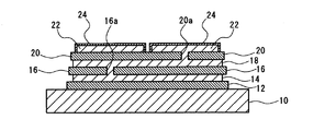
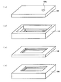
図1に示すように、本発明による金属−セラミックス接合基板の実施の形態は、平面形状が略矩形の放熱用金属ベース板10と、この放熱用金属ベース板10の一方の面に直接接合した平面形状が略矩形の第1のセラミックス基板12と、この第1のセラミックス基板12に直接接合した平面形状が略矩形の第1の金属板14と、この第1の金属板14に直接接合した平面形状が略矩形の第2のセラミックス基板16と、この第2のセラミックス基板16に直接接合した平面形状が略矩形の第2の金属板18と、この第2の金属板18に直接接合した平面形状が略矩形の第3のセラミックス基板20と、この第3のセラミックス基板20に直接接合した平面形状が略矩形の金属回路板22と、この金属回路板22の表面を被覆するめっき部24とから構成されている。
As shown in FIG. 1, in the embodiment of the metal / ceramic bonding substrate according to the present invention, the heat dissipating
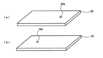
放熱用金属ベース板10と、第1の金属板14と、第2の金属板18と、金属回路板22は、同一の金属材料からなり、アルミニウムまたはアルミニウム合金からなるのが好ましい。また、第2のセラミックス基板16と第3のセラミックス基板20には、それぞれバイアホール用の貫通孔16a、20a(図2(a)および図2(b)参照)が形成されている。これらの貫通孔16a、20a内には、放熱用金属ベース板10などと同じ金属材料が充填されており、それぞれ貫通孔16a、20aの内面に直接接合するとともに、第1の金属板14と第2の金属板18の間および第2の金属板18と金属回路板22の間を接続するバイアコンタクトを形成している。
The heat radiating
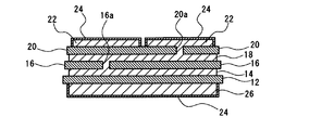
なお、図3に示すように、放熱用金属ベース板10の代わりに、それよりも小さい放熱用金属板26を使用して、この放熱用金属板26の一方の面に第1のセラミックス基板12を直接接合し、他方の面をめっき部24で被覆してもよい。あるいは、図4に示すように、放熱用金属ベース板10の代わりに、冷却フィン付放熱用金属ベース板28を使用してもよい。
As shown in FIG. 3, instead of the heat radiating
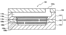
図1に示す実施の形態の金属−セラミックス接合基板は、図5に示すような鋳型100に金属溶湯を流し込んで冷却することにより接合体を製造した後に、エッチングにより金属回路板22を形成し、その表面をニッケルなどでめっきすることによって製造することができる。
The metal-ceramic bonding substrate of the embodiment shown in FIG. 1 forms a
図5および図6(a)〜図6(d)に示すように、鋳型100は、カーボンまたは多孔質金属などの通気性材料からなり、それぞれ平面形状が略矩形の下側鋳型部材102と上側鋳型部材104とから構成されている。下側鋳型部材102に上側鋳型部材104を被せることによって内部に画定される空間の形状および大きさは、図1に示す金属−セラミックス接合基板のエッチング前の形状および大きさに略等しくなっている。
As shown in FIGS. 5 and 6 (a) to 6 (d), the
下側鋳型部材102は、互いに分離可能な底部106と中間部108と上部110とから構成されている。下側鋳型部材102の底部106の上面には、第3のセラミックス基板20と略等しい形状および大きさの第3のセラミックス基板収容部106aが形成され、この第3のセラミックス基板収容部106aの底面には、エッチング前の金属回路板22と略等しい形状および大きさの金属回路板形成部106bが形成されている。下側鋳型部材102の中間部108の略中央部には、中間部108を貫通する略矩形の開口部が形成されている。この開口部の内面には段部が形成され、この開口部の上側の部分が、第2のセラミックス基板16と略等しい形状および大きさの第2のセラミックス基板収容部108aを画定し、下側の部分が、第2の金属板18と略等しい形状および大きさの第2の金属板形成部108bを画定している。下側鋳型部材102の上部110の略中央部には、上部110を貫通する略矩形の開口部が形成されている。この開口部の内面は階段状に形成されており、この開口部の上側の部分が、放熱用金属ベース板10と略等しい形状および大きさの放熱用金属ベース板形成部110aを画定し、中間の部分が、第1のセラミックス基板12と略等しい形状および大きさの第1のセラミックス基板収容部110bを画定し、下側の部分が、第1の金属板14と略等しい形状および大きさの第1の金属板形成部110cを画定している。なお、図5は、セラミックス基板12、16、20が鋳型100内に収容されている状態を示している。
The lower mold member 102 includes a
また、上側鋳型部材104には、金属溶湯を鋳型100内に注湯するための注湯口104aが形成されている。下側鋳型部材102には、放熱用金属ベース板形成部110aに注湯された金属溶湯を第1の金属板形成部110c、第2の金属板形成部108bおよび金属回路板形成部106bに充填するための(図示しない)注湯流路が形成されており、第1、第2および第3のセラミックス基板収容部110b、108a、106aにそれぞれ第1、第2および第3のセラミックス基板12、16、20を収容したときにも放熱用金属ベース板形成部110aが第1の金属板形成部110c、第2の金属板形成部108bおよび金属回路板形成部106bと連通するようになっている。なお、放熱用金属ベース板形成部110aと、第1の金属板形成部110cと、第2の金属板形成部108bと、金属回路板形成部106bとを連通させないで、金属溶湯を充填するための(図示しない)注湯流路を下側鋳型部材102の底部106、中間部108および上部110にそれぞれ形成してもよい。
The
この鋳型100の下側鋳型部材102の底部106の第3のセラミックス基板収容部106a内に第3のセラミックス基板20を収容し、その上に中間部108を載せた後に第2のセラミックス基板収容部108a内に第2のセラミックス基板16を収容し、その上に上部110を載せた後に第1のセラミックス基板収容部110b内に第1のセラミックス基板12を収容し、下側鋳型部材102に上側鋳型部材104を被せた後、注湯口104aから放熱用金属ベース板形成部110a内に金属溶湯を注湯し、(図示しない)溶湯流路を介して第1の金属板形成部110c、第2の金属板形成部108bおよび金属回路板形成部106bまで金属溶湯を充填し、その後、冷却して金属溶湯を固化させることにより、放熱用金属ベース板10、第1、第2および第3のセラミックス基板12、16、20、第1および第2の金属板14、16、およびエッチング前の金属回路板22が一体に接合した金属−セラミックス接合基板を製造することができる。
The third
このように、ろう材を使用しないで、放熱用金属ベース板10と、金属板14、16と、金属回路板22と、複数のセラミックス基板12、16、20とを直接接合して多層構造の金属−セラミックス接合基板を製造することにより、ろう材を使用した場合に生じ易いボイドが生じ難くなり、ろう材を介して金属板を重ねる必要がないので金属板とセラミックス基板の間の位置精度および信頼性を向上させることができる。すなわち、所望の精度の鋳型を設計して作製すれば、所望の精度の多層構造の金属−セラミックス接合基板を量産することができる。また、金属溶湯を鋳型に流し込むだけで多層構造の金属−セラミックス接合基板を製造することができるので、製造コストを低減することができ、生産性にも優れている。さらに、最も外側のセラミックス基板にそのセラミックス基板より大きい放熱部を接合する場合、ろう材を使用して接合すると、ヒートサイクル後にセラミックス基板より大きい放熱部から受ける大きな熱応力によってセラミックス基板にクラックが発生して信頼性を低下させる場合があるが、ろう材を使用しないで直接接合すると、そのようなクラックの発生を防止することができ、板状またはフィン状の放熱部を容易に接合することができる。
Thus, without using a brazing material, the heat dissipating
なお、必要に応じて、放熱用金属ベース板10と金属回路板22をニッケルなどでめっきすれば、半田付け性や耐候性などを向上させることができる。
If necessary, if the
また、セラミックス基板12、16、20は、AlN、Al2O3、Si3N4またはSiCを主成分とする材質からなるのが好ましく、基板の特性やコストなどによって最適な材質を選択すればよい。また、各セラミックス基板12、16、20の材質や形状が同一である必要はなく、溶湯接合法では、セラミックス基板12、16、20の材質や形状に左右されることなく多層構造の金属−セラミックス接合基板を製造することができる。一方、ろう材を使用して多層構造の金属−セラミックス接合基板を製造する場合には、セラミックス基板12、16、20の材質や形状に応じて、ろう材の(組成や形状などの)種類を適当に選択する必要があり、多層構造の金属−セラミックス接合基板の設計が複雑になり、放熱用金属ベース板10と、金属板14、16と、金属回路板22と、複数のセラミックス基板12、16、20とを一度に接合することができない場合がある。
The
以下、本発明による金属−セラミックス接合基板およびその製造方法の実施例について詳細に説明する。 Hereinafter, examples of the metal / ceramic bonding substrate and the manufacturing method thereof according to the present invention will be described in detail.
図5に示す鋳型100と同様のカーボン製の鋳型を用意し、この鋳型の下側鋳型部材の第3のセラミックス基板収容部内に、直径3mmの貫通穴を有し、46mm×46mm×0.635mmの大きさの窒化アルミニウム基板を収容し、第2のセラミックス基板収容部内に、直径3mmの貫通穴を有し、48mm×48mm×0.635mmの大きさの窒化アルミニウム基板を収容し、第1のセラミックス基板収容部内に、50mm×50mm×0.635mmの大きさの窒化アルミニウム基板を収容した。なお、金属回路板形成部の大きさは44mm×44mm×0.5mmであり、第3のセラミックス基板収容部と第2のセラミックス基板収容部の間の第2の金属板形成部の大きさは45mm×45mm×0.5mmであり、第2のセラミックス基板収容部と第1のセラミックス基板収容部の間の第1の金属板形成部の大きさは47mm×47mm×0.5mmであり、第1のセラミックス基板収容部の上の放熱用金属ベース板形成部の大きさは60mm×60mm×6mmである。
A carbon mold similar to the
次に、下側鋳型部材に上側鋳型部材を被せて炉内に入れ、炉内を酸素濃度100ppm以下の窒素雰囲気にした。この状態で750℃まで加熱し、溶融状態のアルミニウムを圧入し、酸化被膜を取り除きながら、鋳型内に流し込んだ。その後、鋳型を冷却してアルミニウムを凝固させ、さらに室温まで冷却した。このようにして接合体を製造し、この接合体を鋳型から取り出した。 Next, the lower mold member was covered with the upper mold member and placed in a furnace, and the furnace was filled with a nitrogen atmosphere having an oxygen concentration of 100 ppm or less. In this state, the mixture was heated to 750 ° C., molten aluminum was pressed into the mold and poured into the mold while removing the oxide film. Thereafter, the mold was cooled to solidify the aluminum, and further cooled to room temperature. In this way, a joined body was produced, and the joined body was taken out from the mold.
その後、回路用アルミニウム板の表面に所定の形状のエッチングレジストを印刷し、塩化第二鉄溶液によってエッチング処理を行って回路パターンを形成しながら、セラミックス基板の端部のアルミニウムを除去した後、レジストを剥離した。このようにして形成したアルミニウム回路板にニッケルめっきを施した。 After that, an etching resist of a predetermined shape is printed on the surface of the circuit aluminum plate, and the aluminum is removed from the edge of the ceramic substrate while forming a circuit pattern by performing an etching process with a ferric chloride solution. Was peeled off. The aluminum circuit board thus formed was subjected to nickel plating.
また、放熱用金属ベース板の裏面をフライス盤により機械加工して1mm研削し、凹凸を50μm以下にした。このようにして得られたサンプルに対して、−40℃で30分間保持、25℃で10分間保持、125℃で30分間保持、25℃で10分間保持を1サイクルとするヒートサイクルを3000回行った後、各々の接合界面を超音波探傷装置によって調べたところ、接合欠陥が認められず、セラミックス基板にもクラックが認められなかった。 Moreover, the back surface of the metal base plate for heat dissipation was machined with a milling machine and ground by 1 mm to make the unevenness 50 μm or less. The sample thus obtained was subjected to a heat cycle of 3000 times with one cycle of holding at −40 ° C. for 30 minutes, holding at 25 ° C. for 10 minutes, holding at 125 ° C. for 30 minutes, and holding at 25 ° C. for 10 minutes. After the inspection, each bonding interface was examined with an ultrasonic flaw detector. As a result, no bonding defect was observed, and no crack was observed in the ceramic substrate.
10 放熱用金属ベース板
12 第1のセラミックス基板
14 第1の金属板
16 第2のセラミックス基板
16a 貫通孔(バイアホール)
18 第2の金属板
20 第3のセラミックス基板
20a 貫通孔(バイアホール)
22 金属回路板
24 めっき部
26 放熱用金属板
28 冷却フィン付放熱用金属ベース板
100 鋳型
102 下側鋳型部材
104 上側鋳型部材
104a 注湯口
106 底部
106a 第3のセラミックス基板収容部
106b 金属回路板形成部
108 中間部
108a 第2のセラミックス基板収容部
108b 第2の金属板形成部
110 上部
110a 放熱用金属ベース板形成部
110b 第1のセラミックス基板収容部
110c 第1の金属板形成部
DESCRIPTION OF
18
22
Claims (4)
Priority Applications (1)
| Application Number | Priority Date | Filing Date | Title |
|---|---|---|---|
| JP2004246606A JP4565249B2 (en) | 2004-08-26 | 2004-08-26 | Metal-ceramic bonding substrate and manufacturing method thereof |
Applications Claiming Priority (1)
| Application Number | Priority Date | Filing Date | Title |
|---|---|---|---|
| JP2004246606A JP4565249B2 (en) | 2004-08-26 | 2004-08-26 | Metal-ceramic bonding substrate and manufacturing method thereof |
Publications (2)
| Publication Number | Publication Date |
|---|---|
| JP2006066595A JP2006066595A (en) | 2006-03-09 |
| JP4565249B2 true JP4565249B2 (en) | 2010-10-20 |
Family
ID=36112800
Family Applications (1)
| Application Number | Title | Priority Date | Filing Date |
|---|---|---|---|
| JP2004246606A Active JP4565249B2 (en) | 2004-08-26 | 2004-08-26 | Metal-ceramic bonding substrate and manufacturing method thereof |
Country Status (1)
| Country | Link |
|---|---|
| JP (1) | JP4565249B2 (en) |
Cited By (3)
| Publication number | Priority date | Publication date | Assignee | Title |
|---|---|---|---|---|
| KR101206918B1 (en) | 2011-04-19 | 2012-11-30 | (주)태린 | Method for joining dissimilar material by high energy density laser with detecting temperature |
| WO2014034245A1 (en) | 2012-08-31 | 2014-03-06 | 三菱マテリアル株式会社 | Power module substrate and power module |
| US9018534B2 (en) | 2011-04-20 | 2015-04-28 | Sotaro Oi | Method of manufacturing power module substrate and power module substrate |
Families Citing this family (10)
| Publication number | Priority date | Publication date | Assignee | Title |
|---|---|---|---|---|
| JP2011073194A (en) * | 2009-09-29 | 2011-04-14 | Dowa Metaltech Kk | Metal-ceramics joint base and method of manufacturing the same |
| JP5389595B2 (en) * | 2009-09-30 | 2014-01-15 | Dowaメタルテック株式会社 | Metal-ceramic bonding substrate and manufacturing method thereof |
| JP5837754B2 (en) * | 2011-03-23 | 2015-12-24 | Dowaメタルテック株式会社 | Metal-ceramic bonding substrate and manufacturing method thereof |
| JP5966275B2 (en) * | 2011-08-10 | 2016-08-10 | 三菱マテリアル株式会社 | Power module substrate manufacturing method |
| JP5831419B2 (en) * | 2012-09-27 | 2015-12-09 | 三菱マテリアル株式会社 | Power module substrate |
| JP6224960B2 (en) * | 2012-09-27 | 2017-11-01 | Dowaメタルテック株式会社 | Heat sink and manufacturing method thereof |
| EP2838325B1 (en) * | 2013-08-16 | 2021-06-16 | NGK Insulators, Ltd. | Ceramic circuit board and electronic device |
| JP6327105B2 (en) | 2014-10-17 | 2018-05-23 | 三菱電機株式会社 | Semiconductor device |
| JP2017212316A (en) * | 2016-05-25 | 2017-11-30 | Dowaホールディングス株式会社 | Metal-ceramic bonding substrate and manufacturing method thereof |
| JP6837365B2 (en) * | 2017-03-28 | 2021-03-03 | 三菱電機株式会社 | Metal-ceramic bonding substrate and its manufacturing method |
Citations (7)
| Publication number | Priority date | Publication date | Assignee | Title |
|---|---|---|---|---|
| JPH1093244A (en) * | 1996-09-18 | 1998-04-10 | Toshiba Corp | Multilayer silicon nitride circuit board |
| JP2001160682A (en) * | 1999-12-01 | 2001-06-12 | Sumitomo Metal Mining Co Ltd | Method of manufacturing multilayer ceramic wiring board |
| JP2001250723A (en) * | 2000-03-07 | 2001-09-14 | Tdk Corp | High-q high-frequency coil and its manufacturing method |
| JP2002283041A (en) * | 2001-03-23 | 2002-10-02 | Taiheiyo Cement Corp | Laminated structural member and its producing method |
| JP2003086747A (en) * | 2001-09-10 | 2003-03-20 | Hitachi Ltd | Insulation circuit board, its manufacturing method and semiconductor power element using the same |
| JP2004105978A (en) * | 2002-09-13 | 2004-04-08 | Dowa Mining Co Ltd | Manufacturing apparatus for metal-ceramic composite member, casting mold for manufacturing, and manufacturing method |
| JP2004115337A (en) * | 2002-09-27 | 2004-04-15 | Dowa Mining Co Ltd | Aluminum-ceramic bonded body |
-
2004
- 2004-08-26 JP JP2004246606A patent/JP4565249B2/en active Active
Patent Citations (7)
| Publication number | Priority date | Publication date | Assignee | Title |
|---|---|---|---|---|
| JPH1093244A (en) * | 1996-09-18 | 1998-04-10 | Toshiba Corp | Multilayer silicon nitride circuit board |
| JP2001160682A (en) * | 1999-12-01 | 2001-06-12 | Sumitomo Metal Mining Co Ltd | Method of manufacturing multilayer ceramic wiring board |
| JP2001250723A (en) * | 2000-03-07 | 2001-09-14 | Tdk Corp | High-q high-frequency coil and its manufacturing method |
| JP2002283041A (en) * | 2001-03-23 | 2002-10-02 | Taiheiyo Cement Corp | Laminated structural member and its producing method |
| JP2003086747A (en) * | 2001-09-10 | 2003-03-20 | Hitachi Ltd | Insulation circuit board, its manufacturing method and semiconductor power element using the same |
| JP2004105978A (en) * | 2002-09-13 | 2004-04-08 | Dowa Mining Co Ltd | Manufacturing apparatus for metal-ceramic composite member, casting mold for manufacturing, and manufacturing method |
| JP2004115337A (en) * | 2002-09-27 | 2004-04-15 | Dowa Mining Co Ltd | Aluminum-ceramic bonded body |
Cited By (6)
| Publication number | Priority date | Publication date | Assignee | Title |
|---|---|---|---|---|
| KR101206918B1 (en) | 2011-04-19 | 2012-11-30 | (주)태린 | Method for joining dissimilar material by high energy density laser with detecting temperature |
| US9018534B2 (en) | 2011-04-20 | 2015-04-28 | Sotaro Oi | Method of manufacturing power module substrate and power module substrate |
| DE102012206276B4 (en) | 2011-04-20 | 2023-02-02 | Mitsubishi Materials Corporation | Method of manufacturing a power module substrate and power module substrate |
| WO2014034245A1 (en) | 2012-08-31 | 2014-03-06 | 三菱マテリアル株式会社 | Power module substrate and power module |
| KR20150052044A (en) | 2012-08-31 | 2015-05-13 | 미쓰비시 마테리알 가부시키가이샤 | Power module substrate and power module |
| US9615442B2 (en) | 2012-08-31 | 2017-04-04 | Mitsubishi Materials Corporation | Power module substrate and power module |
Also Published As
| Publication number | Publication date |
|---|---|
| JP2006066595A (en) | 2006-03-09 |
Similar Documents
| Publication | Publication Date | Title |
|---|---|---|
| JP4565249B2 (en) | Metal-ceramic bonding substrate and manufacturing method thereof | |
| JP4028452B2 (en) | Electronic component mounting substrate and manufacturing method thereof | |
| JP2017212316A (en) | Metal-ceramic bonding substrate and manufacturing method thereof | |
| JP5837754B2 (en) | Metal-ceramic bonding substrate and manufacturing method thereof | |
| JP2010109132A (en) | Thermoelectric module package and method of manufacturing the same | |
| JP2004115337A (en) | Aluminum-ceramic bonded body | |
| JP5619437B2 (en) | Method for producing metal / ceramic bonding substrate | |
| JP2008218938A (en) | Metal-ceramics bonded substrate | |
| JP4496404B2 (en) | Metal-ceramic bonding substrate and manufacturing method thereof | |
| JP4806803B2 (en) | Metal-ceramic bonding substrate and manufacturing method thereof | |
| JP5176042B2 (en) | Electronic component mounting board manufacturing apparatus and manufacturing method | |
| JP5780777B2 (en) | Ceramic circuit board and electronic device using the same | |
| JP5631446B2 (en) | Method for producing metal / ceramic bonding substrate | |
| JP5960522B2 (en) | Ceramic circuit board and electronic device using the same | |
| JP6799392B2 (en) | Metal-ceramic bonded substrate and its manufacturing method | |
| JP2006286754A (en) | Metal-ceramic bonding substrate | |
| JP2011077389A (en) | Metal-ceramic bonded substrate and method of manufacturing the same | |
| JP2006351927A (en) | Semiconductor device, circuit board, and electric connection box | |
| WO2020262015A1 (en) | Metal-ceramic joined substrate and manufacturing method thereof | |
| JP2011073194A (en) | Metal-ceramics joint base and method of manufacturing the same | |
| JP6367701B2 (en) | Circuit board and manufacturing method thereof | |
| JP6317178B2 (en) | Circuit board and electronic device | |
| JP2020050548A (en) | Metal-ceramic bonded substrate, and method of producing the same | |
| JP2016046430A (en) | Circuit board and electronic device | |
| JP7267030B2 (en) | METAL-CERAMIC BONDING SUBSTRATE AND MANUFACTURING METHOD THEREOF |
Legal Events
| Date | Code | Title | Description |
|---|---|---|---|
| A621 | Written request for application examination |
Free format text: JAPANESE INTERMEDIATE CODE: A621 Effective date: 20070625 |
|
| A977 | Report on retrieval |
Free format text: JAPANESE INTERMEDIATE CODE: A971007 Effective date: 20071101 |
|
| A131 | Notification of reasons for refusal |
Free format text: JAPANESE INTERMEDIATE CODE: A131 Effective date: 20100518 |
|
| A521 | Request for written amendment filed |
Free format text: JAPANESE INTERMEDIATE CODE: A523 Effective date: 20100528 |
|
| TRDD | Decision of grant or rejection written | ||
| A01 | Written decision to grant a patent or to grant a registration (utility model) |
Free format text: JAPANESE INTERMEDIATE CODE: A01 Effective date: 20100706 |
|
| A01 | Written decision to grant a patent or to grant a registration (utility model) |
Free format text: JAPANESE INTERMEDIATE CODE: A01 |
|
| A711 | Notification of change in applicant |
Free format text: JAPANESE INTERMEDIATE CODE: A712 Effective date: 20100714 |
|
| A61 | First payment of annual fees (during grant procedure) |
Free format text: JAPANESE INTERMEDIATE CODE: A61 Effective date: 20100715 |
|
| A521 | Request for written amendment filed |
Free format text: JAPANESE INTERMEDIATE CODE: A821 Effective date: 20100714 |
|
| R150 | Certificate of patent or registration of utility model |
Ref document number: 4565249 Country of ref document: JP Free format text: JAPANESE INTERMEDIATE CODE: R150 Free format text: JAPANESE INTERMEDIATE CODE: R150 |
|
| FPAY | Renewal fee payment (event date is renewal date of database) |
Free format text: PAYMENT UNTIL: 20130813 Year of fee payment: 3 |
|
| R250 | Receipt of annual fees |
Free format text: JAPANESE INTERMEDIATE CODE: R250 |
|
| R250 | Receipt of annual fees |
Free format text: JAPANESE INTERMEDIATE CODE: R250 |
|
| R250 | Receipt of annual fees |
Free format text: JAPANESE INTERMEDIATE CODE: R250 |
|
| R250 | Receipt of annual fees |
Free format text: JAPANESE INTERMEDIATE CODE: R250 |
|
| R250 | Receipt of annual fees |
Free format text: JAPANESE INTERMEDIATE CODE: R250 |
|
| R250 | Receipt of annual fees |
Free format text: JAPANESE INTERMEDIATE CODE: R250 |
|
| R250 | Receipt of annual fees |
Free format text: JAPANESE INTERMEDIATE CODE: R250 |
|
| R250 | Receipt of annual fees |
Free format text: JAPANESE INTERMEDIATE CODE: R250 |
|
| R250 | Receipt of annual fees |
Free format text: JAPANESE INTERMEDIATE CODE: R250 |
|
| R250 | Receipt of annual fees |
Free format text: JAPANESE INTERMEDIATE CODE: R250 |
|
| R250 | Receipt of annual fees |
Free format text: JAPANESE INTERMEDIATE CODE: R250 |