WO2014034245A1 - Power module substrate and power module - Google Patents
Power module substrate and power module Download PDFInfo
- Publication number
- WO2014034245A1 WO2014034245A1 PCT/JP2013/067645 JP2013067645W WO2014034245A1 WO 2014034245 A1 WO2014034245 A1 WO 2014034245A1 JP 2013067645 W JP2013067645 W JP 2013067645W WO 2014034245 A1 WO2014034245 A1 WO 2014034245A1
- Authority
- WO
- WIPO (PCT)
- Prior art keywords
- substrate
- ceramic substrate
- power module
- circuit layer
- metal plate
- Prior art date
Links
Images


Classifications
-
- H—ELECTRICITY
- H05—ELECTRIC TECHNIQUES NOT OTHERWISE PROVIDED FOR
- H05K—PRINTED CIRCUITS; CASINGS OR CONSTRUCTIONAL DETAILS OF ELECTRIC APPARATUS; MANUFACTURE OF ASSEMBLAGES OF ELECTRICAL COMPONENTS
- H05K1/00—Printed circuits
- H05K1/02—Details
- H05K1/0201—Thermal arrangements, e.g. for cooling, heating or preventing overheating
- H05K1/0203—Cooling of mounted components
-
- H—ELECTRICITY
- H01—ELECTRIC ELEMENTS
- H01L—SEMICONDUCTOR DEVICES NOT COVERED BY CLASS H10
- H01L23/00—Details of semiconductor or other solid state devices
- H01L23/34—Arrangements for cooling, heating, ventilating or temperature compensation ; Temperature sensing arrangements
- H01L23/36—Selection of materials, or shaping, to facilitate cooling or heating, e.g. heatsinks
- H01L23/373—Cooling facilitated by selection of materials for the device or materials for thermal expansion adaptation, e.g. carbon
- H01L23/3735—Laminates or multilayers, e.g. direct bond copper ceramic substrates
-
- H—ELECTRICITY
- H01—ELECTRIC ELEMENTS
- H01L—SEMICONDUCTOR DEVICES NOT COVERED BY CLASS H10
- H01L23/00—Details of semiconductor or other solid state devices
- H01L23/34—Arrangements for cooling, heating, ventilating or temperature compensation ; Temperature sensing arrangements
- H01L23/42—Fillings or auxiliary members in containers or encapsulations selected or arranged to facilitate heating or cooling
- H01L23/433—Auxiliary members in containers characterised by their shape, e.g. pistons
- H01L23/4334—Auxiliary members in encapsulations
-
- H—ELECTRICITY
- H05—ELECTRIC TECHNIQUES NOT OTHERWISE PROVIDED FOR
- H05K—PRINTED CIRCUITS; CASINGS OR CONSTRUCTIONAL DETAILS OF ELECTRIC APPARATUS; MANUFACTURE OF ASSEMBLAGES OF ELECTRICAL COMPONENTS
- H05K1/00—Printed circuits
- H05K1/02—Details
- H05K1/0271—Arrangements for reducing stress or warp in rigid printed circuit boards, e.g. caused by loads, vibrations or differences in thermal expansion
-
- H—ELECTRICITY
- H05—ELECTRIC TECHNIQUES NOT OTHERWISE PROVIDED FOR
- H05K—PRINTED CIRCUITS; CASINGS OR CONSTRUCTIONAL DETAILS OF ELECTRIC APPARATUS; MANUFACTURE OF ASSEMBLAGES OF ELECTRICAL COMPONENTS
- H05K1/00—Printed circuits
- H05K1/02—Details
- H05K1/0296—Conductive pattern lay-out details not covered by sub groups H05K1/02 - H05K1/0295
- H05K1/0298—Multilayer circuits
-
- H—ELECTRICITY
- H05—ELECTRIC TECHNIQUES NOT OTHERWISE PROVIDED FOR
- H05K—PRINTED CIRCUITS; CASINGS OR CONSTRUCTIONAL DETAILS OF ELECTRIC APPARATUS; MANUFACTURE OF ASSEMBLAGES OF ELECTRICAL COMPONENTS
- H05K1/00—Printed circuits
- H05K1/02—Details
- H05K1/03—Use of materials for the substrate
- H05K1/0306—Inorganic insulating substrates, e.g. ceramic, glass
-
- H—ELECTRICITY
- H05—ELECTRIC TECHNIQUES NOT OTHERWISE PROVIDED FOR
- H05K—PRINTED CIRCUITS; CASINGS OR CONSTRUCTIONAL DETAILS OF ELECTRIC APPARATUS; MANUFACTURE OF ASSEMBLAGES OF ELECTRICAL COMPONENTS
- H05K1/00—Printed circuits
- H05K1/02—Details
- H05K1/09—Use of materials for the conductive, e.g. metallic pattern
-
- H—ELECTRICITY
- H05—ELECTRIC TECHNIQUES NOT OTHERWISE PROVIDED FOR
- H05K—PRINTED CIRCUITS; CASINGS OR CONSTRUCTIONAL DETAILS OF ELECTRIC APPARATUS; MANUFACTURE OF ASSEMBLAGES OF ELECTRICAL COMPONENTS
- H05K1/00—Printed circuits
- H05K1/02—Details
- H05K1/11—Printed elements for providing electric connections to or between printed circuits
- H05K1/115—Via connections; Lands around holes or via connections
-
- H—ELECTRICITY
- H05—ELECTRIC TECHNIQUES NOT OTHERWISE PROVIDED FOR
- H05K—PRINTED CIRCUITS; CASINGS OR CONSTRUCTIONAL DETAILS OF ELECTRIC APPARATUS; MANUFACTURE OF ASSEMBLAGES OF ELECTRICAL COMPONENTS
- H05K1/00—Printed circuits
- H05K1/18—Printed circuits structurally associated with non-printed electric components
- H05K1/181—Printed circuits structurally associated with non-printed electric components associated with surface mounted components
-
- H—ELECTRICITY
- H01—ELECTRIC ELEMENTS
- H01L—SEMICONDUCTOR DEVICES NOT COVERED BY CLASS H10
- H01L23/00—Details of semiconductor or other solid state devices
- H01L23/48—Arrangements for conducting electric current to or from the solid state body in operation, e.g. leads, terminal arrangements ; Selection of materials therefor
- H01L23/488—Arrangements for conducting electric current to or from the solid state body in operation, e.g. leads, terminal arrangements ; Selection of materials therefor consisting of soldered or bonded constructions
- H01L23/498—Leads, i.e. metallisations or lead-frames on insulating substrates, e.g. chip carriers
- H01L23/49811—Additional leads joined to the metallisation on the insulating substrate, e.g. pins, bumps, wires, flat leads
-
- H—ELECTRICITY
- H01—ELECTRIC ELEMENTS
- H01L—SEMICONDUCTOR DEVICES NOT COVERED BY CLASS H10
- H01L23/00—Details of semiconductor or other solid state devices
- H01L23/48—Arrangements for conducting electric current to or from the solid state body in operation, e.g. leads, terminal arrangements ; Selection of materials therefor
- H01L23/488—Arrangements for conducting electric current to or from the solid state body in operation, e.g. leads, terminal arrangements ; Selection of materials therefor consisting of soldered or bonded constructions
- H01L23/498—Leads, i.e. metallisations or lead-frames on insulating substrates, e.g. chip carriers
- H01L23/49861—Lead-frames fixed on or encapsulated in insulating substrates
-
- H—ELECTRICITY
- H01—ELECTRIC ELEMENTS
- H01L—SEMICONDUCTOR DEVICES NOT COVERED BY CLASS H10
- H01L2924/00—Indexing scheme for arrangements or methods for connecting or disconnecting semiconductor or solid-state bodies as covered by H01L24/00
- H01L2924/0001—Technical content checked by a classifier
- H01L2924/0002—Not covered by any one of groups H01L24/00, H01L24/00 and H01L2224/00
-
- H—ELECTRICITY
- H05—ELECTRIC TECHNIQUES NOT OTHERWISE PROVIDED FOR
- H05K—PRINTED CIRCUITS; CASINGS OR CONSTRUCTIONAL DETAILS OF ELECTRIC APPARATUS; MANUFACTURE OF ASSEMBLAGES OF ELECTRICAL COMPONENTS
- H05K2201/00—Indexing scheme relating to printed circuits covered by H05K1/00
- H05K2201/01—Dielectrics
- H05K2201/0137—Materials
- H05K2201/017—Glass ceramic coating, e.g. formed on inorganic substrate
Definitions
- the present invention relates to a power module substrate and a power module used in a semiconductor device that controls a large current and a high voltage.
- This application claims priority based on Japanese Patent Application No. 2012-191607 for which it applied to Japan on August 31, 2012, and uses the content here.
- a metal plate forming a conductor pattern layer is laminated on one surface of a ceramic substrate, and an electronic component such as a semiconductor chip is soldered on the conductor pattern layer, and the other side of the ceramic substrate is A metal plate serving as a heat dissipation layer is formed on the surface, and a heat sink is joined to the heat dissipation layer.
- a metal plate is joined to the surface of the ceramic substrate by brazing.
- the brazing material foil is temporarily fixed to the surface of the ceramic substrate by the surface tension of the volatile organic medium, and the conductor pattern layer punched from the base material is temporarily fixed to the surface of the brazing material foil.
- the power module substrate in which the metal plate and the ceramic substrate are brazed is formed by heating the substrate in order to volatilize the volatile organic medium and pressurizing them in the thickness direction.
- this type of power module substrate in addition to the function as an insulating substrate and the function as a heat dissipation substrate, the function as a wiring substrate has been demanded along with the recent high integration, and it becomes multilayered. It is being considered.
- Patent Document 2 discloses a structure in which a metal column is provided in a through hole formed in a ceramic substrate, and the metal plates on both sides of the ceramic substrate are connected to each other by this metal column.
- the present invention has been made in view of such circumstances, and further improves a power cycle property and a heat cycle property, and a power module substrate having a multilayer structure and a substrate for the power module that can cope with higher integration. It aims at providing the used power module.
- a plurality of circuit layer metal plates made of copper or a copper alloy are joined in a laminated state via the first ceramic substrate, and in the through-hole formed in the first ceramic substrate.
- a metal member for connecting both circuit layer metal plates disposed on both surfaces of the first ceramic substrate is inserted, and the second ceramic substrate is bonded to one surface of the laminated circuit layer metal plate.
- a heat radiation layer metal plate made of aluminum or an aluminum alloy is bonded to the surface of the second ceramic substrate opposite to the circuit layer metal plate.
- a plurality of circuit layer metal plates that are laminated via the first ceramic substrate are connected to each other by a metal member, so that a multi-layer circuit layer is formed and a highly integrated circuit layer is constructed. Can do.
- the circuit layer is formed of copper or copper alloy having excellent thermal conductivity, heat from the mounted semiconductor element can be quickly dissipated, and the solder layer for fixing the semiconductor element can be distorted or cracked. The solder layer can be maintained soundly for a long period of time without causing the above, and the power cycle performance can be improved.
- the metal plate for the heat dissipation layer made of aluminum or aluminum alloy is joined to the other surface of the second ceramic substrate, the generation of stress due to the difference in thermal expansion with the ceramic substrate is alleviated, and the ceramic substrate is cracked or cracked. Can be prevented and heat cycle performance can be improved.
- the metal plate for the circuit layer disposed between the first ceramic substrate and the second ceramic substrate is connected to an external connection projecting outward from the first ceramic substrate.
- the lead terminal portion may be formed integrally.
- the lead terminal part is formed on the metal plate for the uppermost circuit layer, it is necessary to form a circuit by bypassing the electronic circuit for wiring to the outside because electronic components are mounted.
- it tends to be large in the surface direction, when using a middle metal plate, it is sufficient to form the lead terminal part at an appropriate position on the outer periphery, and the power module substrate can be made small by suppressing the expansion of the flat area. It is possible to
- the second ceramic substrate is formed with a protruding portion that protrudes outward from the first ceramic substrate, and at least a part of the lead terminal portion is formed of the second ceramic substrate. It is good to be supported on the protrusion. A load in the case of connecting a bonding wire or the like to the lead terminal portion can be partially borne by the second ceramic substrate, and deformation of the lead terminal portion can be prevented.
- a hole is formed in the middle circuit layer formed between the first ceramic substrate and the second ceramic substrate, and has an opening at an end of the middle circuit layer. It is good to be.
- the power module of the present invention includes the power module substrate, and an electronic component joined on the circuit layer metal plate disposed on the first ceramic substrate, wherein the heat dissipation layer metal plate includes: The power module substrate and the electronic component are sealed by a resin mold except for the surface.
- the resin is poured into and around the multiple substrates and metal plates and electronic components stacked between the electronic component and the heat dissipation layer.
- the resin mold can be firmly held on the module substrate, and the bondability of the electronic component can be secured satisfactorily.
- the thickness of the resin on the circuit layer side on which the electronic component is mounted becomes uniform, and when the power cycle is loaded , The bonding reliability of the solder layer can be maintained.
- the resin also enters the hole, and the resin mold can be more firmly held on the power module substrate.
- the power module with a heat sink includes the power module substrate, a heat sink joined to the heat dissipation layer metal plate of the power module substrate, and the circuit layer disposed on the first ceramic substrate.
- An electronic component joined on a metal plate, the power module substrate and the electronic component are sealed with a resin mold, and a part of the heat sink is covered with the resin mold Also good.
- the circuit layer metal plate is formed of copper or a copper alloy
- the heat dissipation layer metal plate is formed of aluminum or an aluminum alloy, so that both power cycle characteristics and heat cycle characteristics are improved. It is possible to obtain a multilayer power module substrate that can be used for long-term and highly reliable.
- FIG. 3 is a plan view taken along the line BB in FIG. 1.
- FIG. 2 is an enlarged cross-sectional view showing the vicinity of a joint portion in FIG. 1.
- FIG. 5 shows the dimensional relationship between the through-hole of the ceramic substrate before joining, and the convex part of the metal plate for circuit layers.
- FIG. 4 is a plan view similar to FIG. 3 for explaining the configuration of a middle circuit layer which is another embodiment of the power module substrate of the present invention.
- FIG. 5 is a plan view similar to FIG. 3 for explaining the configuration of a middle circuit layer which is still another embodiment of the power module substrate of the present invention.
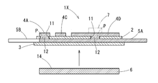
- the power module substrate 1 is formed by laminating a plurality of ceramic substrates 2, 3, circuit layer metal plates 4A to 4E, 5A, 5B, and a heat dissipation layer metal plate 6.
- the electronic parts 7 are mounted on a part of the circuit layer metal plates 4A to 4E (4D and 4E in the illustrated example) that are joined to each other by brazing or the like and arranged at the uppermost stage.
- the heat sink 8 is joined to the metal plate 6 for the heat radiation layer disposed on the surface.
- the ceramic substrates 2 and 3 are formed of AlN, Al 2 O 3 , SiC, or the like, for example, to a thickness of 0.32 mm to 1.0 mm.
- the circuit layer metal plates 4A to 4E, 5A, 5B are formed of pure copper or copper alloy such as oxygen-free copper or tough pitch copper, and the heat dissipation layer metal plate 6 is pure aluminum or aluminum alloy having a purity of 99.90% or more. It is formed by.
- the thickness of these metal plates is, for example, 0.25 mm to 2.5 mm.
- the metal plate 6 for layers is joined.
- an active metal brazing material of Ag-27.4 mass% Cu-2.0 mass% Ti is used for joining the ceramic substrates 2 and 3 and the circuit layer metal plates 4A to 4E, 5A, 5B.
- An Al—Si based or Al—Ge based brazing material is used for joining the second ceramic substrate 3 and the heat radiation layer metal plate 6.
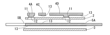
- circuit layer metal plates 4A to 4E, 5A, 5B are arranged on both surfaces of the first ceramic substrate 2. Yes.
- the second ceramic substrate 3 is joined to the circuit layer metal plates 5A and 5B opposite to the uppermost circuit layer metal plates 4A to 4E, and the circuit layer metal plates 5A and 5B of the second ceramic substrate 3
- the heat sink layer metal plate 6 is joined to the opposite surface.
- the circuit layer metal plates 4A to 4E, 5A, and 5B are arranged at the uppermost level, two at the middle level between the two ceramic substrates, and at the lowermost level, 1 level.
- a sheet of heat radiation layer metal plate 6 is provided.
- the uppermost five circuit layer metal plates 4A to 4E are arranged in the middle position (1C) and two on each side (4A, 4B and 4D, 4E).
- the circuit layer metal plates 5A and 5B between the two ceramic substrates 2 and 3 have lengths that can connect the metal plates 4A and 4D and the metal plates 4B and 4E, respectively, disposed at both uppermost positions.
- the portion is formed in an elongated strip shape protruding from the edge of the first ceramic substrate 2, and the two pieces are arranged side by side in parallel and are opposite to each other from the edge of the first ceramic substrate 2. It protrudes in the direction.
- the upper circuit layer is formed by the five circuit layer metal plates 4A to 4E on the first ceramic substrate 2, and the middle layer is formed by the circuit layer metal plates 5A and 5B disposed between the two ceramic substrates 2 and 3.
- the circuit layer is formed.
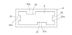
- both circuit layer metal plates 5A and 5B are arranged with a space therebetween, so that these circuit layer metal plates 5A and 5B are disposed.
- a hole 51 is formed so as to be surrounded by the ceramic substrates 2 and 3, and an opening 51a is opened at the end.
- the metal plates 4A and 4D and the metal plates 4B and 4E on both sides in the uppermost stage are paired and connected to each other via the middle metal plates 5A and 5B so as to be connected below the intermediate metal plate 4C. It is in an electrical connection state.
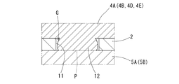
- connection form four through holes 11 are formed in the first ceramic substrate 2 and 4 except for the metal plate 4C at the middle position among the above five uppermost circuit layer metal plates 4A to 4E.
- Convex portions (corresponding to the metal member of the present invention) 12 are integrally formed in a columnar shape on one side of each of the metal plates 4A, 4B, 4D, and 4E, and these convex portions 12 are inserted into the through holes 11, respectively.
- the structure is such that it is bonded to the middle metal plates 5A and 5B between the ceramic substrates 2 and 3. In this case, as shown in FIG.
- the convex portion 12 is joined to the middle metal plates 5A and 5B, the joint P to the middle metal plates 5A and 5B, and the lower surfaces of the metal plates 4A, 4B, 4D and 4E.
- the middle part of the through hole 11 is plastically deformed and slightly expanded in diameter, but a gap G is formed between the inner peripheral surface of the through hole 11.
- a structure having two or a plurality of second ceramic substrates 3 may also be employed.
- the projecting end portions of the middle circuit layer metal plates 5A, 5B from the first ceramic substrate 2 to the side are bent from the middle as shown by the two-dot chain lines in FIG. Used as In this case, since the second ceramic substrate 3 is formed to have a larger plane area than the first ceramic substrate 2, the outer peripheral portion of the second ceramic substrate 3 protrudes outward from the first ceramic substrate 2, A part of the lead terminal portion 15 is supported on the upper surface of the protruding portion 3 a of the second ceramic substrate 3 protruding outward from the first ceramic substrate 2.
- the first ceramic substrate 2 having the through holes 11 can be obtained by forming the through holes in the green sheet before firing of the ceramics by press working and firing. Its outer shape is processed after firing. The second ceramic substrate 3 having no through hole is subjected to external processing after firing the green sheet.
- the metal plates 4C, 5A, 5B, and 6 have the brazing materials 13 and 14 temporarily fixed to the surface with a volatile organic medium such as octanediol, and are integrally formed by pressing.
- a metal plate with a brazing material foil is attached.
- an active metal brazing material 13 of, for example, Ag-27.4 mass% Cu-2.0 mass% Ti is attached to one surface of the uppermost metal plate 4C and both surfaces of the central metal plates 5A and 5B.
- An Al—Si-based or Al—Ge-based brazing material 14 is attached to one surface of the lowermost metal plate 6.
- the metal plates 4A, 4B, 4D, and 4E having the convex portion 12 are formed by previously forming the convex portion 12 on one side by press working, and the convex portion 12 is excluded. Thus, it forms by sticking the brazing material foil which pierced the hole to the plane around the convex part 12.
- the convex portion 12 formed in this way is larger than the thickness of the ceramic substrate 2 having the through hole 11 and is a length that slightly protrudes from the ceramic substrate 2 when inserted into the through hole 11 as shown in FIG. Is set. Taking into account the dimensional variation of the thickness of the ceramic substrate 2, it is set to a length 0.02 mm to 0.2 mm larger than the maximum tolerance, for example, 0.05 mm larger. Further, the outer diameter D1 of the convex portion 12 and the inner diameter D2 of the through hole 11 of the ceramic substrate 2 are such that the convex portion 12 expands during pressurization, which will be described later, so that a gap G is formed even in the expanded diameter state.
- the outer diameter D1 of the convex portion 12 is 1.0 mm to 20 mm, and the inner diameter D2 of the through hole 11 of the ceramic substrate 2 is 1.1 mm to 28 mm.
- the outer diameter D1 of the convex portion 12 is 10 mm, and the inner diameter D2 of the through hole 11 is 13 mm.
- the two ceramic substrates 2 and 3 and the metal plates 4A to 4E, 5A, 5B, and 6 formed in this way are joined in two steps.
- First, the two ceramic substrates 2 and 3 are joined to the uppermost stage.
- the metal plates 4A to 4E and the middle metal plates 5A and 5B are joined first (primary joining), and then the lowermost metal plate 6 and the heat sink 8 are joined (secondary joining) to the primary joined body.
- secondary joining the ceramic substrates 2 and 3 and the uppermost metal plates 4A to 4E and the middle metal plates 5A and 5B are alternately overlapped to correspond to the convex portions 12 of the metal plates 4A, 4B, 4D, and 4E.
- the pressure device 110 includes a base plate 111, guide posts 112 vertically attached to the four corners of the upper surface of the base plate 111, a fixed plate 113 fixed to the upper ends of the guide posts 112, and the base plates 111.
- a pressing plate 114 supported by a guide post 112 so as to freely move up and down between the fixing plate 113 and a spring provided between the fixing plate 113 and the pressing plate 114 to urge the pressing plate 114 downward.
- urging means 115 is provided by a guide post 112 so as to freely move up and down between the fixing plate 113 and a spring provided between the fixing plate 113 and the pressing plate 114 to urge the pressing plate 114 downward.
- the fixed plate 113 and the pressing plate 114 are arranged in parallel to the base plate 111, and the above-described laminate S is arranged between the base plate 111 and the pressing plate 114.
- Carbon sheets 116 are disposed on both sides of the laminate S to make the pressure uniform.
- the pressure device 110 and the pressure device 110 are installed in a heating furnace (not shown) and heated to a brazing temperature of, for example, 850 ° C. for brazing.
- a brazing temperature of, for example, 850 ° C. for brazing.
- Ti which is an active metal in the brazing material is preferentially diffused on the surfaces of the ceramic substrates 2 and 3 to form TiN, and the metal plates 4A to 4E, 5A, Join 5B.
- the urging force of the urging means 115 is set in advance so that a load higher than the yield point acts on the convex portions 12 of the metal plates 4A, 4B, 4D, and 4E during the brazing. Since the yield stress at around 850 ° C.
- the urging force of the urging means 115 at normal temperature is set.
- the convex portion 12 is plastically deformed and crushed during brazing, while being joined to the central metal plates 5A and 5B, and the metal plate 4A around the convex portion 12
- the planes of 4E to 4E are in close contact with the surface of the ceramic substrate 2, and a uniform bonding state in the surface direction can be obtained.
- the convex portion 12 partially enlarges the diameter, but as described above, a gap G is formed between the convex portion 12 and the inner peripheral surface of the through hole 11 in a state where the diameter is enlarged. Therefore, the convex portion 12 is not pressed against the inner peripheral surface of the through hole 11.
- the second ceramic substrate 3 of the primary bonded body 1X is laminated so as to overlap the surface of the metal plate 6 constituting the lowermost layer on which the brazing material 14 is attached. Then, using the pressurizing device 110 described above, these are heated and brazed in a vacuum.
- the applied pressure in this case is, for example, 0.68 MPa (7 kgf / cm 2 ), and the heating temperature is, for example, 630 ° C.
- the power module substrate 1 manufactured in this way has an electronic component 7 mounted on a part of the uppermost metal plates 4A to 4E and a heat sink on the lowermost metal plate 6 as shown by a chain line in FIG. 8 is attached for use. Further, the projecting end portions of the middle stage circuit layer metal plates 5A and 5B from the first ceramic substrate 2 are bent to form lead terminals 15 for external connection.
- the heat sink 8 is formed, for example, by extrusion molding of A6063 aluminum alloy. In the example of illustration, it extrudes in the direction orthogonal to a paper surface, and the straight fin 21 is formed in strip
- a plurality of straight fins 21 having a thickness of 4 mm and a height of 15 mm along the extrusion direction are formed on one surface of a plate-like portion 22 having a 50 mm square and a thickness of 5 mm.
- the heat sink 8 is fixed to the metal plate 6 by brazing, screwing or the like.
- an Al—Si or Al—Ge brazing material is used as the brazing material and the applied pressure is, for example, 0.68 MPa (7 kgf / cm 2 )
- the temperature for example, brazing at 610 ° C. is possible.
- this power module substrate 1 has a gap G formed between the convex portion 12 and the inner peripheral surface of the through hole 11, even if thermal expansion and contraction is repeated due to a temperature cycle during use, The thermal stress at the portion is reduced, peeling of the joint portion and cracking of the ceramic substrates 2 and 3 are prevented, and high reliability can be maintained as a power module substrate. Further, the heat generated in the electronic component 7 mounted on the uppermost metal plates 4D and 4E is also transferred from the metal plates 4D and 4E to the central metal plates 5A and 5B via the convex portions 12.
- the convex portion 12 when the convex portion 12 is disposed directly below the electronic component 7, heat is transferred linearly from the metal plates 4D and 4E to the central metal plates 5A and 5B via the convex portion 12 to quickly dissipate heat. be able to.
- the outer diameter D1 of the convex portion 12 should be large. For example, if the cross-sectional area is larger than the projected area of the electronic component 7, the electronic component 7 is mounted on the extension of the convex portion 12. Excellent heat dissipation.
- the convex portion 12 having a large cross-sectional area is preferable because the current density is reduced.
- the electronic component can be sealed with a resin mold for the purpose of fixing and insulating the electronic component.
- FIG. 10 shows a power module in which a resin mold is formed.
- the power module substrate 1 and the electronic component 7 are made of a resin such as an epoxy resin, except for the surface of the heat dissipation layer metal plate 6. Resin-sealed by a mold 56.
- FIG. 11 shows an embodiment in which a resin mold is formed on a power module with a heat sink with a heat sink attached.
- the resin mold 62 integrally covers the electronic component 7 and the power module substrate 1 and is joined to a part of the heat sink 8, specifically, to the metal plate 6 for the heat dissipation layer. It is provided so as to cover the top plate portion of the heat sink 8. Since the joint portion with the heat sink 8 is also covered with the resin mold 62, it is firmly integrated as a whole.
- this invention is not limited to the said embodiment, A various change can be added in the range which does not deviate from the meaning of this invention.
- a copper layer having a thickness of about 0.4 ⁇ m is formed on one surface of the heat radiation layer metal plate 6 constituting the lowermost layer by vapor deposition or the like, and the second ceramic of the primary bonded body 1X is formed thereon.
- the substrates 3 may be stacked, and these may be bonded by a transient liquid phase bonding method (Transient Liquid Phase Diffusion Bonding).
- a copper layer deposited on the surface of the metal plate 6 is interposed at the interface between the metal plate 6 and the ceramic substrate 3, and the copper is first contained in the aluminum of the metal plate 6 by heating.
- the copper concentration in the vicinity of the copper layer of the metal plate 6 increases and the melting point decreases, thereby forming a metal liquid phase at the bonding interface in the eutectic region of aluminum and copper. If the temperature is kept constant in a state where the metal liquid phase is formed, the metal liquid phase contacts and reacts with the ceramic substrate 3 at a constant temperature for a certain time, and copper further diffuses into the aluminum.
- the copper concentration in the metal liquid phase gradually decreases and the melting point increases, and solidification proceeds while the temperature is kept constant.
- the metal plate 6 is cooled to room temperature.
- the pressure at that time is a 98kPa (1kgf / cm 2) ⁇ 3.4MPa (35kgf / cm 2), at 10 -3 to 10 -6 in a vacuum of Pa, is heated for 0.5 hours at 600 ° C. .
- the bonding of the ceramic substrate 3 and the metal plate 6 and the bonding of the metal plate 6 and the heat sink 8 can be performed simultaneously.
- the embodiment has been described in which the convex portions are integrally formed on the metal plate.
- the columnar metal member 31 is formed separately from the metal plates 4 and 5 to penetrate the ceramic substrate 2. It is good also as what arrange
- joints P are formed on both end surfaces of the metal member 31.
- convex portions (metal members) 12 ⁇ / b> A and 12 ⁇ / b> B are formed on both metal plates 4 and 5, respectively, and joined at a midpoint of the length of the through hole 11 of the ceramic substrate 2. It is good. In this case, the joint portion P is formed in the middle position of the through hole 11.
- this metal member is not formed in a columnar shape, but is formed in a columnar shape having a polygonal cross section, and the through hole is also formed in the same polygon, so that the metal member can be prevented from rotating in the through hole.
- the metal plate can be easily positioned in the structure.
- the present invention is not limited to this, and the metal plates may be laminated with three or more ceramic substrates.
- the first ceramic substrate 2 having the through holes 11 is obtained by forming the through holes in the green sheet before firing the ceramics and then firing the ceramic sheets.
- the through hole 11 may be formed by processing or the like.
- the middle-stage circuit layer metal plates 5A and 5B are formed in the shape of an elongated strip as shown in FIG. 3, but may be bent and formed into an L-shape in plan view as shown in FIG.
- the bent holes 51 can also be formed by arranging the bent portions so as to face each other.
- the hole 51 opened at the end of the middle circuit layer is not limited to the structure penetrating from one end of the circuit layer to the other end, but as shown in FIG. It can also be set as the hole 51 notched in the edge part of the metal plate 5 for an object. Also in this case, since the resin enters the hole 51 and is cured, the resin mold can be firmly held on the power module substrate.
- the heat sink may have a pin-like fin formed by forging or the like, or a plate-like shape called a heat sink. These types are combined and defined as a heat sink.
- the present invention can be applied to a power module substrate and a power module that can be used for a semiconductor device that controls a large current and a high voltage, and can cope with high integration by being multilayered.
Abstract
Provided is a power module substrate, which has further improved power cycle characteristics and heat cycle characteristics, and which is applicable to high integration, said power module substrate having a multi-layer structure.
A plurality of circuit layer metal plates (4A-4E, 5A, 5B) formed of copper or a copper alloy are bonded in a laminated state with a first ceramic substrate (2) therebetween, a metal member (12) is inserted into a through hole (11) formed in the first ceramic substrate (2), said metal member bringing both the circuit layer metal plates disposed on both the surfaces of the first ceramic substrate (2) into a connected state, second ceramic substrates (3) are bonded to the surfaces of the laminated-state circuit layer metal plates (4A-4E, 5A, 5B), said surfaces being on the one side of the laminated-state circuit layer metal plates, and a heat dissipating layer metal plate (6) formed of aluminum or an aluminum alloy is bonded to the surface of the second ceramic substrate (3), said surface being on the reverse side of the circuit layer metal plates (4A-4E, 5A, 5B).
Description
本発明は、大電流、高電圧を制御する半導体装置に用いられるパワーモジュール用基板及びパワーモジュールに関する。
本願は、2012年8月31日に日本国に出願された特願2012-191607号に基づき優先権を主張し、その内容をここに援用する。 The present invention relates to a power module substrate and a power module used in a semiconductor device that controls a large current and a high voltage.
This application claims priority based on Japanese Patent Application No. 2012-191607 for which it applied to Japan on August 31, 2012, and uses the content here.
従来のパワーモジュールとして、セラミックス基板の一方の面に、導体パターン層を形成する金属板が積層され、この導体パターン層の上に半導体チップ等の電子部品がはんだ付けされるとともに、セラミックス基板の他方の面に放熱層となる金属板が形成され、この放熱層にヒートシンクが接合された構成のものが知られている。
このパワーモジュールに用いられるパワーモジュール用基板においては、セラミックス基板の表面に金属板をろう付けにより接合している。例えば、特許文献1では、セラミックス基板の表面に揮発性有機媒体の表面張力によってろう材箔を仮固定するとともに、そのろう材箔の表面に基材から打ち抜かれた導体パターン層を仮固定した状態で加熱し、揮発性有機媒体を揮発させ、これらを厚さ方向に加圧することにより、金属板とセラミックス基板とをろう付けしたパワーモジュール用基板を形成している。
一方、この種のパワーモジュール用基板としては、絶縁基板としての機能、放熱基板としての機能の他に、近年の高集積化に伴い、配線基板としての機能も求められてきており、多層化することが検討されている。 As a conventional power module, a metal plate forming a conductor pattern layer is laminated on one surface of a ceramic substrate, and an electronic component such as a semiconductor chip is soldered on the conductor pattern layer, and the other side of the ceramic substrate is A metal plate serving as a heat dissipation layer is formed on the surface, and a heat sink is joined to the heat dissipation layer.
In the power module substrate used in this power module, a metal plate is joined to the surface of the ceramic substrate by brazing. For example, inPatent Document 1, the brazing material foil is temporarily fixed to the surface of the ceramic substrate by the surface tension of the volatile organic medium, and the conductor pattern layer punched from the base material is temporarily fixed to the surface of the brazing material foil. The power module substrate in which the metal plate and the ceramic substrate are brazed is formed by heating the substrate in order to volatilize the volatile organic medium and pressurizing them in the thickness direction.
On the other hand, as this type of power module substrate, in addition to the function as an insulating substrate and the function as a heat dissipation substrate, the function as a wiring substrate has been demanded along with the recent high integration, and it becomes multilayered. It is being considered.
このパワーモジュールに用いられるパワーモジュール用基板においては、セラミックス基板の表面に金属板をろう付けにより接合している。例えば、特許文献1では、セラミックス基板の表面に揮発性有機媒体の表面張力によってろう材箔を仮固定するとともに、そのろう材箔の表面に基材から打ち抜かれた導体パターン層を仮固定した状態で加熱し、揮発性有機媒体を揮発させ、これらを厚さ方向に加圧することにより、金属板とセラミックス基板とをろう付けしたパワーモジュール用基板を形成している。
一方、この種のパワーモジュール用基板としては、絶縁基板としての機能、放熱基板としての機能の他に、近年の高集積化に伴い、配線基板としての機能も求められてきており、多層化することが検討されている。 As a conventional power module, a metal plate forming a conductor pattern layer is laminated on one surface of a ceramic substrate, and an electronic component such as a semiconductor chip is soldered on the conductor pattern layer, and the other side of the ceramic substrate is A metal plate serving as a heat dissipation layer is formed on the surface, and a heat sink is joined to the heat dissipation layer.
In the power module substrate used in this power module, a metal plate is joined to the surface of the ceramic substrate by brazing. For example, in
On the other hand, as this type of power module substrate, in addition to the function as an insulating substrate and the function as a heat dissipation substrate, the function as a wiring substrate has been demanded along with the recent high integration, and it becomes multilayered. It is being considered.
例えば、特許文献2に開示の金属-セラミックス接合基板(パワーモジュール用基板)では、バイアホール用の貫通孔が形成された複数のセラミックス基板と、これらセラミックス基板の間に介在するアルミニウム製の金属板とが多層構造に設けられている。この場合、金属板は、鋳型の中で積み重ねたセラミックス基板に金属溶湯を流し込んで固化することにより形成されており、このため、セラミックス基板に形成しておいた貫通孔内にも金属溶湯が入り込んで固化され、その貫通孔内の金属を介してセラミックス基板の両側の金属板相互が電気的接続状態とされている。
また、特許文献3には、セラミックス基板に形成した貫通孔内に金属柱を設け、この金属柱でセラミックス基板両面の金属板を接続状態としたものが開示されている。 For example, in the metal-ceramic bonding substrate (power module substrate) disclosed inPatent Document 2, a plurality of ceramic substrates in which through holes for via holes are formed, and an aluminum metal plate interposed between these ceramic substrates Are provided in a multilayer structure. In this case, the metal plate is formed by pouring the molten metal into the ceramic substrates stacked in the mold and solidifying them. For this reason, the molten metal also enters the through holes formed in the ceramic substrate. The metal plates on both sides of the ceramic substrate are electrically connected through the metal in the through hole.
Patent Document 3 discloses a structure in which a metal column is provided in a through hole formed in a ceramic substrate, and the metal plates on both sides of the ceramic substrate are connected to each other by this metal column.
また、特許文献3には、セラミックス基板に形成した貫通孔内に金属柱を設け、この金属柱でセラミックス基板両面の金属板を接続状態としたものが開示されている。 For example, in the metal-ceramic bonding substrate (power module substrate) disclosed in
このような多層構造のパワーモジュール用基板において、さらなる高集積化に対応して、電子部品の発熱に伴う熱ストレスが頻繁に作用するため、より高いパワーサイクル性が求められ、また、環境温度変化に伴うヒートサイクル性の向上も求められている。
In such a multilayer power module substrate, thermal stress due to heat generation of electronic components frequently acts in response to higher integration, and therefore higher power cycle characteristics are required, and environmental temperature changes There is also a need for improved heat cycle performance.
本発明は、このような事情に鑑みてなされたものであり、パワーサイクル性、ヒートサイクル性をさらに向上させ、より高集積化に対応できる多層構造のパワーモジュール用基板及びそのパワーモジュール用基板を用いたパワーモジュールを提供することを目的とする。
The present invention has been made in view of such circumstances, and further improves a power cycle property and a heat cycle property, and a power module substrate having a multilayer structure and a substrate for the power module that can cope with higher integration. It aims at providing the used power module.
本発明のパワーモジュール用基板は、銅又は銅合金からなる複数の回路層用金属板が第1セラミックス基板を介して積層状態に接合されるとともに、前記第1セラミックス基板に形成した貫通孔内に、該第1セラミックス基板の両面に配置される両回路層用金属板を接続状態とする金属部材が挿入され、前記積層状態の回路層用金属板の一方側の面に第2セラミックス基板が接合され、該第2セラミックス基板の前記回路層用金属板とは反対側の面にアルミニウム又はアルミニウム合金からなる放熱層用金属板が接合されていることを特徴とする。
In the power module substrate of the present invention, a plurality of circuit layer metal plates made of copper or a copper alloy are joined in a laminated state via the first ceramic substrate, and in the through-hole formed in the first ceramic substrate. A metal member for connecting both circuit layer metal plates disposed on both surfaces of the first ceramic substrate is inserted, and the second ceramic substrate is bonded to one surface of the laminated circuit layer metal plate. A heat radiation layer metal plate made of aluminum or an aluminum alloy is bonded to the surface of the second ceramic substrate opposite to the circuit layer metal plate.
第1セラミックス基板を介して積層状態とされた複数の回路層用金属板が金属部材により接続状態とされることにより、多層の回路層が形成されており、高集積の回路層を構築することができる。しかも、この回路層を熱伝導性に優れる銅又は銅合金により形成したので、搭載される半導体素子からの熱を速やかに放散することができるとともに、該半導体素子を固着するはんだ層に歪みやクラック等を生じさせることがなく、該はんだ層を長期的に健全に維持することができ、パワーサイクル性を向上させることができる。
一方、第2セラミックス基板の他方の面にはアルミニウム又はアルミニウム合金からなる放熱層用金属板を接合したので、セラミックス基板との熱膨張差に伴う応力発生を緩和して、セラミックス基板の割れやクラックの発生が防止され、ヒートサイクル性を向上させることができる。 A plurality of circuit layer metal plates that are laminated via the first ceramic substrate are connected to each other by a metal member, so that a multi-layer circuit layer is formed and a highly integrated circuit layer is constructed. Can do. In addition, since the circuit layer is formed of copper or copper alloy having excellent thermal conductivity, heat from the mounted semiconductor element can be quickly dissipated, and the solder layer for fixing the semiconductor element can be distorted or cracked. The solder layer can be maintained soundly for a long period of time without causing the above, and the power cycle performance can be improved.
On the other hand, since the metal plate for the heat dissipation layer made of aluminum or aluminum alloy is joined to the other surface of the second ceramic substrate, the generation of stress due to the difference in thermal expansion with the ceramic substrate is alleviated, and the ceramic substrate is cracked or cracked. Can be prevented and heat cycle performance can be improved.
本発明のパワーモジュール用基板において、前記第1セラミックス基板と第2セラミックス基板との間に配置される中段の回路層用金属板に、前記第1セラミックス基板よりも外方に突出する外部接続用リード端子部が一体に形成されているとよい。
最上段の回路層用金属板は、電子部品が搭載されるため、外部への配線のために電子回路を迂回して回路を形成する必要があるなど、これにリード端子部を形成する場合は面方向に大きくなり易いが、中段の金属板を利用する場合は、その外周のうちの適宜の位置にリード端子部を形成すればよく、平面積の拡大を抑制してパワーモジュール用基板を小型化することが可能である。 In the power module substrate according to the present invention, the metal plate for the circuit layer disposed between the first ceramic substrate and the second ceramic substrate is connected to an external connection projecting outward from the first ceramic substrate. The lead terminal portion may be formed integrally.
When the lead terminal part is formed on the metal plate for the uppermost circuit layer, it is necessary to form a circuit by bypassing the electronic circuit for wiring to the outside because electronic components are mounted. Although it tends to be large in the surface direction, when using a middle metal plate, it is sufficient to form the lead terminal part at an appropriate position on the outer periphery, and the power module substrate can be made small by suppressing the expansion of the flat area. It is possible to
本発明のパワーモジュール用基板において、前記第2セラミックス基板に前記第1セラミックス基板よりも外方に突出する突出部が形成されるとともに、前記リード端子部の少なくとも一部が前記第2セラミックス基板の突出部の上に支持されているとよい。
リード端子部にボンディングワイヤ等を接続する場合の負荷を第2セラミックス基板に一部負担させることができ、リード端子部の変形を防止することができる。 In the power module substrate according to the present invention, the second ceramic substrate is formed with a protruding portion that protrudes outward from the first ceramic substrate, and at least a part of the lead terminal portion is formed of the second ceramic substrate. It is good to be supported on the protrusion.
A load in the case of connecting a bonding wire or the like to the lead terminal portion can be partially borne by the second ceramic substrate, and deformation of the lead terminal portion can be prevented.
本発明のパワーモジュール用基板において、前記第1セラミックス基板と前記第2セラミックス基板との間に形成される中段の回路層に、該中段の回路層の端部に開口する穴部が形成されているとよい。
In the power module substrate of the present invention, a hole is formed in the middle circuit layer formed between the first ceramic substrate and the second ceramic substrate, and has an opening at an end of the middle circuit layer. It is good to be.
本発明のパワーモジュールは、前記パワーモジュール用基板と、前記第1セラミックス基板の上に配置される前記回路層用金属板の上に接合された電子部品とを備え、前記放熱層用金属板の表面を除いて前記パワーモジュール用基板及び前記電子部品が樹脂モールドにより封止されていることを特徴とする。
The power module of the present invention includes the power module substrate, and an electronic component joined on the circuit layer metal plate disposed on the first ceramic substrate, wherein the heat dissipation layer metal plate includes: The power module substrate and the electronic component are sealed by a resin mold except for the surface.
電子部品とパワーモジュール用基板とを樹脂モールドにより封止することで、電子部品と放熱層との間に積層された複数の基板及び金属板及び電子部品の周囲や隙間に樹脂が流し込まれ、パワーモジュール用基板に樹脂モールドを強固に保持することができ、電子部品の接合性を良好に確保することができる。
また、電子部品と反りの抑制されたパワーモジュール用基板とを樹脂モールドにより封止することで、電子部品の搭載された回路層側の樹脂の厚みが均一となり、パワーサイクルが負荷された際に、前記はんだ層の接合信頼性を維持することができる。
特に、中段の回路層に穴部を有する場合、樹脂が穴部にも入り込み、パワーモジュール用基板に樹脂モールドをより強固に保持することができる。 By sealing the electronic component and the power module substrate with a resin mold, the resin is poured into and around the multiple substrates and metal plates and electronic components stacked between the electronic component and the heat dissipation layer. The resin mold can be firmly held on the module substrate, and the bondability of the electronic component can be secured satisfactorily.
Also, by sealing the electronic component and the power module substrate with reduced warpage with a resin mold, the thickness of the resin on the circuit layer side on which the electronic component is mounted becomes uniform, and when the power cycle is loaded , The bonding reliability of the solder layer can be maintained.
In particular, when the middle circuit layer has a hole, the resin also enters the hole, and the resin mold can be more firmly held on the power module substrate.
本発明のヒートシンク付パワーモジュールは、前記パワーモジュール用基板と、前記パワーモジュール用基板の前記放熱層用金属板に接合されたヒートシンクと、前記第1セラミックス基板の上に配置される前記回路層用金属板の上に接合された電子部品とを備え、前記パワーモジュール用基板及び前記電子部品が樹脂モールドにより封止されているとともに、前記ヒートシンクの一部が前記樹脂モールドに覆われているものとしてもよい。
The power module with a heat sink according to the present invention includes the power module substrate, a heat sink joined to the heat dissipation layer metal plate of the power module substrate, and the circuit layer disposed on the first ceramic substrate. An electronic component joined on a metal plate, the power module substrate and the electronic component are sealed with a resin mold, and a part of the heat sink is covered with the resin mold Also good.
本発明によれば、回路層用金属板を銅又は銅合金により形成し、放熱層用金属板をアルミニウム又はアルミニウム合金により形成したことにより、パワーサイクル性とヒートサイクル性との両方の特性を高く発揮することができ、長期的に信頼性の高い多層のパワーモジュール用基板を得ることができる。
According to the present invention, the circuit layer metal plate is formed of copper or a copper alloy, and the heat dissipation layer metal plate is formed of aluminum or an aluminum alloy, so that both power cycle characteristics and heat cycle characteristics are improved. It is possible to obtain a multilayer power module substrate that can be used for long-term and highly reliable.
以下、本発明の一実施形態を、図面を参照しながら説明する。
このパワーモジュール用基板1は、図1及び図2に示すように、複数のセラミックス基板2,3と、回路層用金属板4A~4E,5A,5Bと、放熱層用金属板6とが積層状態とされ、相互にろう付け等により接合されており、最上段に配置される回路層用金属板4A~4Eの一部(図示例では4D,4E)に電子部品7が搭載され、最下段に配置される放熱層用金属板6にヒートシンク8が接合される。
セラミックス基板2,3は、AlN、Al2O3、SiC等により、例えば0.32mm~1.0mmの厚さに形成される。また、回路層用金属板4A~4E,5A,5Bは無酸素銅やタフピッチ銅等の純銅又は銅合金により形成され、放熱層用金属板6は純度99.90%以上の純アルミニウム又はアルミニウム合金により形成されている。これら金属板の厚さは、例えば0.25mm~2.5mmとされる。
これらの接合は、後述するように2回に分けて行われ、両セラミックス基板2,3と回路層用金属板4A~4E,5A,5Bとをまず接合した後、第2セラミックス基板3に放熱層用金属板6を接合する。この場合、両セラミックス基板2,3と回路層用金属板4A~4E,5A,5Bとの接合には、例えばAg-27.4質量%Cu-2.0質量%Tiの活性金属ろう材が用いられ、第2セラミックス基板3と放熱層用金属板6との接合には、Al-Si系又はAl-Ge系のろう材が用いられる。 Hereinafter, an embodiment of the present invention will be described with reference to the drawings.
As shown in FIGS. 1 and 2, thepower module substrate 1 is formed by laminating a plurality of ceramic substrates 2, 3, circuit layer metal plates 4A to 4E, 5A, 5B, and a heat dissipation layer metal plate 6. The electronic parts 7 are mounted on a part of the circuit layer metal plates 4A to 4E (4D and 4E in the illustrated example) that are joined to each other by brazing or the like and arranged at the uppermost stage. The heat sink 8 is joined to the metal plate 6 for the heat radiation layer disposed on the surface.
The ceramic substrates 2 and 3 are formed of AlN, Al 2 O 3 , SiC, or the like, for example, to a thickness of 0.32 mm to 1.0 mm. The circuit layer metal plates 4A to 4E, 5A, 5B are formed of pure copper or copper alloy such as oxygen-free copper or tough pitch copper, and the heat dissipation layer metal plate 6 is pure aluminum or aluminum alloy having a purity of 99.90% or more. It is formed by. The thickness of these metal plates is, for example, 0.25 mm to 2.5 mm.
These bondings are performed in two steps as will be described later. After the ceramic substrates 2 and 3 and the circuit layer metal plates 4A to 4E, 5A and 5B are first bonded, heat is radiated to the second ceramic substrate 3. The metal plate 6 for layers is joined. In this case, for example, an active metal brazing material of Ag-27.4 mass% Cu-2.0 mass% Ti is used for joining the ceramic substrates 2 and 3 and the circuit layer metal plates 4A to 4E, 5A, 5B. An Al—Si based or Al—Ge based brazing material is used for joining the second ceramic substrate 3 and the heat radiation layer metal plate 6.
このパワーモジュール用基板1は、図1及び図2に示すように、複数のセラミックス基板2,3と、回路層用金属板4A~4E,5A,5Bと、放熱層用金属板6とが積層状態とされ、相互にろう付け等により接合されており、最上段に配置される回路層用金属板4A~4Eの一部(図示例では4D,4E)に電子部品7が搭載され、最下段に配置される放熱層用金属板6にヒートシンク8が接合される。
セラミックス基板2,3は、AlN、Al2O3、SiC等により、例えば0.32mm~1.0mmの厚さに形成される。また、回路層用金属板4A~4E,5A,5Bは無酸素銅やタフピッチ銅等の純銅又は銅合金により形成され、放熱層用金属板6は純度99.90%以上の純アルミニウム又はアルミニウム合金により形成されている。これら金属板の厚さは、例えば0.25mm~2.5mmとされる。
これらの接合は、後述するように2回に分けて行われ、両セラミックス基板2,3と回路層用金属板4A~4E,5A,5Bとをまず接合した後、第2セラミックス基板3に放熱層用金属板6を接合する。この場合、両セラミックス基板2,3と回路層用金属板4A~4E,5A,5Bとの接合には、例えばAg-27.4質量%Cu-2.0質量%Tiの活性金属ろう材が用いられ、第2セラミックス基板3と放熱層用金属板6との接合には、Al-Si系又はAl-Ge系のろう材が用いられる。 Hereinafter, an embodiment of the present invention will be described with reference to the drawings.
As shown in FIGS. 1 and 2, the
The
These bondings are performed in two steps as will be described later. After the
また、図示例ではセラミックス基板が第1セラミックス基板2と第2セラミックス基板3との2枚用いられ、第1セラミックス基板2の両面に回路層用金属板4A~4E,5A,5Bが配置されている。最上段の回路層用金属板4A~4Eとは反対側の回路層用金属板5A,5Bに第2セラミックス基板3が接合され、この第2セラミックス基板3の回路層用金属板5A,5Bとは反対側の面に放熱層用金属板6が接合されている。
また、図2及び図3に示すように、回路層用金属板4A~4E,5A,5Bは、最上段に5枚、両セラミックス基板の間の中段に2枚配置され、最下段には1枚の放熱層用金属板6が設けられている。最上段の5枚の回路層用金属板4A~4Eは、中間の位置に1枚(4C)、その両側にそれぞれ2枚ずつ(4A,4Bと4D,4E)配置されている。両セラミックス基板2,3の間の回路層用金属板5A,5Bは、最上段の両側位置に配置されている金属板4A,4D及び金属板4B,4Eをそれぞれ連結し得る長さでかつ一端部が第1セラミックス基板2の端縁から突出する長さの細長い帯板状に形成され、2枚が並んで平行に配置されており、それぞれ、第1セラミックス基板2の端縁から相互に反対方向に向けて突出している。第1セラミックス基板2の上の5枚の回路層用金属板4A~4Eにより上段の回路層が形成され、両セラミックス基板2,3の間に配置される回路層用金属板5A,5Bにより中段の回路層が形成される。そして、この中段の回路層には、図3及び図4に示すように、両回路層用金属板5A,5Bが間隔をあけて配置されていることにより、これら回路層用金属板5A,5Bと両セラミックス基板2,3とに囲まれるように穴51が形成され、その開口部51aが端部に開口している。
そして、最上段における両側の金属板4A,4D及び金属板4B,4Eが組になって、中間位置の金属板4Cの下方で連結するように、中段の金属板5A,5Bを介して相互に電気的接続状態とされている。 In the illustrated example, two ceramic substrates, a firstceramic substrate 2 and a second ceramic substrate 3, are used, and circuit layer metal plates 4A to 4E, 5A, 5B are arranged on both surfaces of the first ceramic substrate 2. Yes. The second ceramic substrate 3 is joined to the circuit layer metal plates 5A and 5B opposite to the uppermost circuit layer metal plates 4A to 4E, and the circuit layer metal plates 5A and 5B of the second ceramic substrate 3 The heat sink layer metal plate 6 is joined to the opposite surface.
As shown in FIGS. 2 and 3, the circuitlayer metal plates 4A to 4E, 5A, and 5B are arranged at the uppermost level, two at the middle level between the two ceramic substrates, and at the lowermost level, 1 level. A sheet of heat radiation layer metal plate 6 is provided. The uppermost five circuit layer metal plates 4A to 4E are arranged in the middle position (1C) and two on each side (4A, 4B and 4D, 4E). The circuit layer metal plates 5A and 5B between the two ceramic substrates 2 and 3 have lengths that can connect the metal plates 4A and 4D and the metal plates 4B and 4E, respectively, disposed at both uppermost positions. The portion is formed in an elongated strip shape protruding from the edge of the first ceramic substrate 2, and the two pieces are arranged side by side in parallel and are opposite to each other from the edge of the first ceramic substrate 2. It protrudes in the direction. The upper circuit layer is formed by the five circuit layer metal plates 4A to 4E on the first ceramic substrate 2, and the middle layer is formed by the circuit layer metal plates 5A and 5B disposed between the two ceramic substrates 2 and 3. The circuit layer is formed. In the middle circuit layer, as shown in FIGS. 3 and 4, both circuit layer metal plates 5A and 5B are arranged with a space therebetween, so that these circuit layer metal plates 5A and 5B are disposed. A hole 51 is formed so as to be surrounded by the ceramic substrates 2 and 3, and an opening 51a is opened at the end.
Then, the metal plates 4A and 4D and the metal plates 4B and 4E on both sides in the uppermost stage are paired and connected to each other via the middle metal plates 5A and 5B so as to be connected below the intermediate metal plate 4C. It is in an electrical connection state.
また、図2及び図3に示すように、回路層用金属板4A~4E,5A,5Bは、最上段に5枚、両セラミックス基板の間の中段に2枚配置され、最下段には1枚の放熱層用金属板6が設けられている。最上段の5枚の回路層用金属板4A~4Eは、中間の位置に1枚(4C)、その両側にそれぞれ2枚ずつ(4A,4Bと4D,4E)配置されている。両セラミックス基板2,3の間の回路層用金属板5A,5Bは、最上段の両側位置に配置されている金属板4A,4D及び金属板4B,4Eをそれぞれ連結し得る長さでかつ一端部が第1セラミックス基板2の端縁から突出する長さの細長い帯板状に形成され、2枚が並んで平行に配置されており、それぞれ、第1セラミックス基板2の端縁から相互に反対方向に向けて突出している。第1セラミックス基板2の上の5枚の回路層用金属板4A~4Eにより上段の回路層が形成され、両セラミックス基板2,3の間に配置される回路層用金属板5A,5Bにより中段の回路層が形成される。そして、この中段の回路層には、図3及び図4に示すように、両回路層用金属板5A,5Bが間隔をあけて配置されていることにより、これら回路層用金属板5A,5Bと両セラミックス基板2,3とに囲まれるように穴51が形成され、その開口部51aが端部に開口している。
そして、最上段における両側の金属板4A,4D及び金属板4B,4Eが組になって、中間位置の金属板4Cの下方で連結するように、中段の金属板5A,5Bを介して相互に電気的接続状態とされている。 In the illustrated example, two ceramic substrates, a first
As shown in FIGS. 2 and 3, the circuit
Then, the
その接続形態としては、第1セラミックス基板2に4個の貫通孔11が形成され、前述の5枚の最上段の回路層用金属板4A~4Eのうちの中間位置の金属板4Cを除く4枚の金属板4A,4B,4D,4Eの片面にそれぞれ凸部(本発明の金属部材に相当)12が円柱状に一体に形成され、これら凸部12がそれぞれ貫通孔11内に挿入し、両セラミックス基板2,3の間の中段の金属板5A,5Bに接合された構造とされている。この場合図5に示すように、凸部12は、中段の金属板5A,5Bに接合され、中段の金属板5A,5Bへの接合部Pと金属板4A,4B,4D及び4Eの下面との中間付近が塑性変形してわずかに拡径した状態とされているが、貫通孔11の内周面との間には隙間Gが形成されている。
As the connection form, four through holes 11 are formed in the first ceramic substrate 2 and 4 except for the metal plate 4C at the middle position among the above five uppermost circuit layer metal plates 4A to 4E. Convex portions (corresponding to the metal member of the present invention) 12 are integrally formed in a columnar shape on one side of each of the metal plates 4A, 4B, 4D, and 4E, and these convex portions 12 are inserted into the through holes 11, respectively. The structure is such that it is bonded to the middle metal plates 5A and 5B between the ceramic substrates 2 and 3. In this case, as shown in FIG. 5, the convex portion 12 is joined to the middle metal plates 5A and 5B, the joint P to the middle metal plates 5A and 5B, and the lower surfaces of the metal plates 4A, 4B, 4D and 4E. The middle part of the through hole 11 is plastically deformed and slightly expanded in diameter, but a gap G is formed between the inner peripheral surface of the through hole 11.
本実施形態では、貫通孔11を有する第1セラミックス基板2と貫通孔11を有しない第2セラミックス基板3との2枚で構成されたパワーモジュール用基板を用いて説明したが、第1セラミックス基板2又は第2セラミックス基板3を複数枚有する構造とすることもできる。
In the present embodiment, the description has been given using the power module substrate composed of the first ceramic substrate 2 having the through hole 11 and the second ceramic substrate 3 not having the through hole 11. A structure having two or a plurality of second ceramic substrates 3 may also be employed.
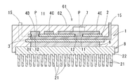
また、中段の回路層用金属板5A,5Bの第1セラミックス基板2から側方への突出端部は、図1の二点鎖線で示すように途中から折り曲げられ、外部接続用リード端子部15として用いられる。
この場合、第2セラミックス基板3は第1セラミックス基板2よりも平面積が大きく形成されていることにより、第2セラミックス基板3の外周部は第1セラミックス基板2よりも外方に突出しており、リード端子部15の一部は、第1セラミックス基板2の外方に突出している第2セラミックス基板3の突出部3aの上面に支持されている。 Further, the projecting end portions of the middle circuit layer metal plates 5A, 5B from the first ceramic substrate 2 to the side are bent from the middle as shown by the two-dot chain lines in FIG. Used as
In this case, since the secondceramic substrate 3 is formed to have a larger plane area than the first ceramic substrate 2, the outer peripheral portion of the second ceramic substrate 3 protrudes outward from the first ceramic substrate 2, A part of the lead terminal portion 15 is supported on the upper surface of the protruding portion 3 a of the second ceramic substrate 3 protruding outward from the first ceramic substrate 2.
この場合、第2セラミックス基板3は第1セラミックス基板2よりも平面積が大きく形成されていることにより、第2セラミックス基板3の外周部は第1セラミックス基板2よりも外方に突出しており、リード端子部15の一部は、第1セラミックス基板2の外方に突出している第2セラミックス基板3の突出部3aの上面に支持されている。 Further, the projecting end portions of the middle circuit
In this case, since the second
次に、このように構成したパワーモジュール用基板1を製造する方法について説明する。
セラミックス基板2,3のうち、貫通孔11を有する第1セラミックス基板2は、セラミックスの焼成前のグリーンシートにプレス加工により貫通孔を形成した後に焼成することにより得ることができる。その外形は焼成後に加工される。貫通孔を有しない第2セラミックス基板3は、グリーンシートを焼成した後に外形加工される。 Next, a method for manufacturing thepower module substrate 1 configured as described above will be described.
Of the ceramic substrates 2 and 3, the first ceramic substrate 2 having the through holes 11 can be obtained by forming the through holes in the green sheet before firing of the ceramics by press working and firing. Its outer shape is processed after firing. The second ceramic substrate 3 having no through hole is subjected to external processing after firing the green sheet.
セラミックス基板2,3のうち、貫通孔11を有する第1セラミックス基板2は、セラミックスの焼成前のグリーンシートにプレス加工により貫通孔を形成した後に焼成することにより得ることができる。その外形は焼成後に加工される。貫通孔を有しない第2セラミックス基板3は、グリーンシートを焼成した後に外形加工される。 Next, a method for manufacturing the
Of the
図6及び図9に示すように、金属板4C,5A,5B,6は、ろう材13,14をオクタンジオール等の揮発性有機媒体等により表面に仮固定しておき、プレス加工によって一体に打ち抜くことにより、ろう材箔を貼り付けた金属板としておく。この場合、最上段の金属板4Cの片面及び中央の金属板5A,5Bの両面に、例えばAg-27.4質量%Cu-2.0質量%Tiの活性金属ろう材13が貼り付けられ、最下段の金属板6には、その片面にAl-Si系又はAl-Ge系のろう材14が貼り付けられる。
また、最上段の金属板4A~4Eのうち、凸部12を有する金属板4A,4B,4D,4Eは、予めプレス加工により片面に凸部12を成形しておき、その凸部12を除くように穴をあけたろう材箔を凸部12の周囲の平面に貼り付けることにより形成される。 As shown in FIGS. 6 and 9, the metal plates 4C, 5A, 5B, and 6 have the brazing materials 13 and 14 temporarily fixed to the surface with a volatile organic medium such as octanediol, and are integrally formed by pressing. By punching, a metal plate with a brazing material foil is attached. In this case, an active metal brazing material 13 of, for example, Ag-27.4 mass% Cu-2.0 mass% Ti is attached to one surface of the uppermost metal plate 4C and both surfaces of the central metal plates 5A and 5B. An Al—Si-based or Al—Ge-based brazing material 14 is attached to one surface of the lowermost metal plate 6.
Of theuppermost metal plates 4A to 4E, the metal plates 4A, 4B, 4D, and 4E having the convex portion 12 are formed by previously forming the convex portion 12 on one side by press working, and the convex portion 12 is excluded. Thus, it forms by sticking the brazing material foil which pierced the hole to the plane around the convex part 12.
また、最上段の金属板4A~4Eのうち、凸部12を有する金属板4A,4B,4D,4Eは、予めプレス加工により片面に凸部12を成形しておき、その凸部12を除くように穴をあけたろう材箔を凸部12の周囲の平面に貼り付けることにより形成される。 As shown in FIGS. 6 and 9, the
Of the
このようにして成形される凸部12は、貫通孔11を有するセラミックス基板2の厚さよりも大きく、図7に示すように、貫通孔11に挿入したときにセラミックス基板2からわずかに突出する長さに設定される。セラミックス基板2の厚さの寸法ばらつきを考慮して、その公差の最大値よりも0.02mm~0.2mm大きい長さ、例えば0.05mm大きい長さに設定される。また、凸部12の外径D1とセラミックス基板2の貫通孔11の内径D2とは、後述する加圧時に凸部12が拡径するので、その拡径状態でも隙間Gが形成されるように凸部12の外径D1は1.0mm~20mm、セラミックス基板2の貫通孔11の内径D2は1.1mm~28mmに形成される。例えば、凸部12の外径D1が10mm、貫通孔11の内径D2は13mmとされる。
The convex portion 12 formed in this way is larger than the thickness of the ceramic substrate 2 having the through hole 11 and is a length that slightly protrudes from the ceramic substrate 2 when inserted into the through hole 11 as shown in FIG. Is set. Taking into account the dimensional variation of the thickness of the ceramic substrate 2, it is set to a length 0.02 mm to 0.2 mm larger than the maximum tolerance, for example, 0.05 mm larger. Further, the outer diameter D1 of the convex portion 12 and the inner diameter D2 of the through hole 11 of the ceramic substrate 2 are such that the convex portion 12 expands during pressurization, which will be described later, so that a gap G is formed even in the expanded diameter state. The outer diameter D1 of the convex portion 12 is 1.0 mm to 20 mm, and the inner diameter D2 of the through hole 11 of the ceramic substrate 2 is 1.1 mm to 28 mm. For example, the outer diameter D1 of the convex portion 12 is 10 mm, and the inner diameter D2 of the through hole 11 is 13 mm.
このようにして形成した2枚のセラミックス基板2,3及び金属板4A~4E,5A,5B,6は、2回に分けて接合され、まず、2枚のセラミックス基板2,3と最上段の金属板4A~4E及び中段の金属板5A,5Bとを先に接合(一次接合)し、その後に、その一次接合体に最下段の金属板6及びヒートシンク8を接合(二次接合)する。
一次接合においては、セラミックス基板2,3と最上段の金属板4A~4E及び中段の金属板5A,5Bとを交互に重ね合わせ、金属板4A,4B,4D,4Eの凸部12を対応するセラミックス基板2の貫通孔11に挿入した状態とし、その積層体Sを図8に示す加圧装置に設置する。
この加圧装置110は、ベース板111と、ベース板111の上面の四隅に垂直に取り付けられたガイドポスト112と、これらガイドポスト112の上端部に固定された固定板113と、これらベース板111と固定板113との間で上下移動自在にガイドポスト112に支持された押圧板114と、固定板113と押圧板114との間に設けられて押圧板114を下方に付勢するばね等の付勢手段115とを備えている。
固定板113および押圧板114は、ベース板111に対して平行に配置されており、ベース板111と押圧板114との間に前述の積層体Sが配置される。積層体Sの両面には加圧を均一にするためにカーボンシート116が配設される。 The two ceramic substrates 2 and 3 and the metal plates 4A to 4E, 5A, 5B, and 6 formed in this way are joined in two steps. First, the two ceramic substrates 2 and 3 are joined to the uppermost stage. The metal plates 4A to 4E and the middle metal plates 5A and 5B are joined first (primary joining), and then the lowermost metal plate 6 and the heat sink 8 are joined (secondary joining) to the primary joined body.
In the primary bonding, the ceramic substrates 2 and 3 and the uppermost metal plates 4A to 4E and the middle metal plates 5A and 5B are alternately overlapped to correspond to the convex portions 12 of the metal plates 4A, 4B, 4D, and 4E. It is set as the state inserted in the through-hole 11 of the ceramic substrate 2, and the laminated body S is installed in the pressurization apparatus shown in FIG.
Thepressure device 110 includes a base plate 111, guide posts 112 vertically attached to the four corners of the upper surface of the base plate 111, a fixed plate 113 fixed to the upper ends of the guide posts 112, and the base plates 111. A pressing plate 114 supported by a guide post 112 so as to freely move up and down between the fixing plate 113 and a spring provided between the fixing plate 113 and the pressing plate 114 to urge the pressing plate 114 downward. And urging means 115.
The fixedplate 113 and the pressing plate 114 are arranged in parallel to the base plate 111, and the above-described laminate S is arranged between the base plate 111 and the pressing plate 114. Carbon sheets 116 are disposed on both sides of the laminate S to make the pressure uniform.
一次接合においては、セラミックス基板2,3と最上段の金属板4A~4E及び中段の金属板5A,5Bとを交互に重ね合わせ、金属板4A,4B,4D,4Eの凸部12を対応するセラミックス基板2の貫通孔11に挿入した状態とし、その積層体Sを図8に示す加圧装置に設置する。
この加圧装置110は、ベース板111と、ベース板111の上面の四隅に垂直に取り付けられたガイドポスト112と、これらガイドポスト112の上端部に固定された固定板113と、これらベース板111と固定板113との間で上下移動自在にガイドポスト112に支持された押圧板114と、固定板113と押圧板114との間に設けられて押圧板114を下方に付勢するばね等の付勢手段115とを備えている。
固定板113および押圧板114は、ベース板111に対して平行に配置されており、ベース板111と押圧板114との間に前述の積層体Sが配置される。積層体Sの両面には加圧を均一にするためにカーボンシート116が配設される。 The two
In the primary bonding, the
The
The fixed
この加圧装置110により加圧した状態で、加圧装置110ごと図示略の加熱炉内に設置し、例えば850℃のろう付け温度に加熱してろう付けする。
このろう付けにおいては、ろう材中の活性金属であるTiが優先的にセラミックス基板2,3の表面に拡散してTiNを形成し、Ag-Cu合金を介して金属板4A~4E,5A,5Bと接合する。
また、このろう付け時に金属板4A,4B,4D,4Eの凸部12に降伏点以上の荷重が作用するように、予め付勢手段115の付勢力を設定しておく。タフピッチ銅の850℃付近での降伏応力は3~4MPa程度であることから、例えば、凸部12の外径D1が10mmとすると、850℃の高温時に、凸部12に231N以上の荷重が作用するように、常温での付勢手段115の付勢力を設定しておく。 In a state where the pressure is applied by thepressure device 110, the pressure device 110 and the pressure device 110 are installed in a heating furnace (not shown) and heated to a brazing temperature of, for example, 850 ° C. for brazing.
In this brazing, Ti which is an active metal in the brazing material is preferentially diffused on the surfaces of the ceramic substrates 2 and 3 to form TiN, and the metal plates 4A to 4E, 5A, Join 5B.
In addition, the urging force of the urging means 115 is set in advance so that a load higher than the yield point acts on theconvex portions 12 of the metal plates 4A, 4B, 4D, and 4E during the brazing. Since the yield stress at around 850 ° C. of tough pitch copper is about 3 to 4 MPa, for example, if the outer diameter D1 of the convex portion 12 is 10 mm, a load of 231 N or more acts on the convex portion 12 at a high temperature of 850 ° C. Thus, the urging force of the urging means 115 at normal temperature is set.
このろう付けにおいては、ろう材中の活性金属であるTiが優先的にセラミックス基板2,3の表面に拡散してTiNを形成し、Ag-Cu合金を介して金属板4A~4E,5A,5Bと接合する。
また、このろう付け時に金属板4A,4B,4D,4Eの凸部12に降伏点以上の荷重が作用するように、予め付勢手段115の付勢力を設定しておく。タフピッチ銅の850℃付近での降伏応力は3~4MPa程度であることから、例えば、凸部12の外径D1が10mmとすると、850℃の高温時に、凸部12に231N以上の荷重が作用するように、常温での付勢手段115の付勢力を設定しておく。 In a state where the pressure is applied by the
In this brazing, Ti which is an active metal in the brazing material is preferentially diffused on the surfaces of the
In addition, the urging force of the urging means 115 is set in advance so that a load higher than the yield point acts on the
このように付勢力を設定しておくことにより、ろう付け時に凸部12が塑性変形して押しつぶされながら、中央の金属板5A,5Bに接合するとともに、この凸部12の周囲の金属板4A~4Eの平面がセラミックス基板2の表面に密接し、面方向に均一な接合状態を得ることができる。
また、接合した後の状態においても、凸部12は部分的に拡径するが、前述したように拡径した状態で凸部12と貫通孔11の内周面との間に隙間Gが形成される設定であるので、凸部12が貫通孔11の内周面に圧迫されることはない。 By setting the urging force in this way, theconvex portion 12 is plastically deformed and crushed during brazing, while being joined to the central metal plates 5A and 5B, and the metal plate 4A around the convex portion 12 The planes of 4E to 4E are in close contact with the surface of the ceramic substrate 2, and a uniform bonding state in the surface direction can be obtained.
Even in the state after joining, theconvex portion 12 partially enlarges the diameter, but as described above, a gap G is formed between the convex portion 12 and the inner peripheral surface of the through hole 11 in a state where the diameter is enlarged. Therefore, the convex portion 12 is not pressed against the inner peripheral surface of the through hole 11.
また、接合した後の状態においても、凸部12は部分的に拡径するが、前述したように拡径した状態で凸部12と貫通孔11の内周面との間に隙間Gが形成される設定であるので、凸部12が貫通孔11の内周面に圧迫されることはない。 By setting the urging force in this way, the
Even in the state after joining, the
次いで、二次接合では、図9に示すように、最下段を構成する金属板6のろう材14が貼り付けられた面の上に一次接合体1Xの第2セラミックス基板3を重ねるように積層し、前述した加圧装置110を用いて、これらを加圧した状態で真空中で加熱してろう付けする。この場合の加圧力としては例えば0.68MPa(7kgf/cm2)、加熱温度としては例えば630℃とされる。
Next, in the secondary bonding, as shown in FIG. 9, the second ceramic substrate 3 of the primary bonded body 1X is laminated so as to overlap the surface of the metal plate 6 constituting the lowermost layer on which the brazing material 14 is attached. Then, using the pressurizing device 110 described above, these are heated and brazed in a vacuum. The applied pressure in this case is, for example, 0.68 MPa (7 kgf / cm 2 ), and the heating temperature is, for example, 630 ° C.
このようにして製造されたパワーモジュール用基板1は、図1に鎖線で示すように、最上段の金属板4A~4Eの一部に電子部品7が搭載され、最下段の金属板6にヒートシンク8が取り付けられて使用に供される。また、中段の回路層用金属板5A,5Bの第1セラミックス基板2からの突出端部は折り曲げられて外部接続用リード端子部15とされる。
なお、ヒートシンク8は、例えばA6063アルミニウム合金の押出成形により形成される。図示例では、紙面に直交する方向に押し出され、その押出方向に沿って帯板状にストレートのフィン21が形成される。寸法的に限定されるものではないが、例えば50mm角で厚さ5mmの板状部22の片面に、押出方向に沿う厚さ4mm、高さ15mmのストレート状のフィン21が複数形成されている。このヒートシンク8は、金属板6にろう付け、ネジ止め等により固定される。なお、ヒートシンク8を金属板6にろう付けする場合は、ろう材としてAl-Si系又はAl-Ge系のろう材を用いて、加圧力としては例えば0.68MPa(7kgf/cm2)、加熱温度としては例えば610℃でろう付けすることが可能である。 Thepower module substrate 1 manufactured in this way has an electronic component 7 mounted on a part of the uppermost metal plates 4A to 4E and a heat sink on the lowermost metal plate 6 as shown by a chain line in FIG. 8 is attached for use. Further, the projecting end portions of the middle stage circuit layer metal plates 5A and 5B from the first ceramic substrate 2 are bent to form lead terminals 15 for external connection.
Theheat sink 8 is formed, for example, by extrusion molding of A6063 aluminum alloy. In the example of illustration, it extrudes in the direction orthogonal to a paper surface, and the straight fin 21 is formed in strip | belt-plate shape along the extrusion direction. Although not limited in size, for example, a plurality of straight fins 21 having a thickness of 4 mm and a height of 15 mm along the extrusion direction are formed on one surface of a plate-like portion 22 having a 50 mm square and a thickness of 5 mm. . The heat sink 8 is fixed to the metal plate 6 by brazing, screwing or the like. When the heat sink 8 is brazed to the metal plate 6, an Al—Si or Al—Ge brazing material is used as the brazing material and the applied pressure is, for example, 0.68 MPa (7 kgf / cm 2 ) As the temperature, for example, brazing at 610 ° C. is possible.
なお、ヒートシンク8は、例えばA6063アルミニウム合金の押出成形により形成される。図示例では、紙面に直交する方向に押し出され、その押出方向に沿って帯板状にストレートのフィン21が形成される。寸法的に限定されるものではないが、例えば50mm角で厚さ5mmの板状部22の片面に、押出方向に沿う厚さ4mm、高さ15mmのストレート状のフィン21が複数形成されている。このヒートシンク8は、金属板6にろう付け、ネジ止め等により固定される。なお、ヒートシンク8を金属板6にろう付けする場合は、ろう材としてAl-Si系又はAl-Ge系のろう材を用いて、加圧力としては例えば0.68MPa(7kgf/cm2)、加熱温度としては例えば610℃でろう付けすることが可能である。 The
The
このパワーモジュール用基板1は、凸部12と貫通孔11の内周面との間に隙間Gが形成されているので、使用時の温度サイクルにより熱伸縮が繰り返されても、貫通孔11の部分での熱応力が軽減され、接合部の剥離やセラミックス基板2,3の割れ等が防止され、パワーモジュール用基板として高い信頼性を維持することができる。
また、最上段の金属板4D,4Eに搭載されている電子部品7で発生する熱は、その金属板4D,4Eから凸部12を経由して中央の金属板5A,5Bにも熱伝達されるが、凸部12が電子部品7の直下に配置される場合は、金属板4D,4Eから凸部12を介して直線的に中央の金属板5A,5Bに熱伝達され、速やかに放熱することができる。この放熱性を高めるためには凸部12の外径D1は大きい方がよく、例えば電子部品7の投影面積よりも大きい横断面積であると、凸部12の延長上に電子部品7を搭載すれば優れた放熱性を発揮する。また、パワーモジュールとしても大電流が流れるので、大きい断面積の凸部12の方が電流密度が小さくなるので好ましい。 Since thispower module substrate 1 has a gap G formed between the convex portion 12 and the inner peripheral surface of the through hole 11, even if thermal expansion and contraction is repeated due to a temperature cycle during use, The thermal stress at the portion is reduced, peeling of the joint portion and cracking of the ceramic substrates 2 and 3 are prevented, and high reliability can be maintained as a power module substrate.
Further, the heat generated in theelectronic component 7 mounted on the uppermost metal plates 4D and 4E is also transferred from the metal plates 4D and 4E to the central metal plates 5A and 5B via the convex portions 12. However, when the convex portion 12 is disposed directly below the electronic component 7, heat is transferred linearly from the metal plates 4D and 4E to the central metal plates 5A and 5B via the convex portion 12 to quickly dissipate heat. be able to. In order to improve the heat dissipation, the outer diameter D1 of the convex portion 12 should be large. For example, if the cross-sectional area is larger than the projected area of the electronic component 7, the electronic component 7 is mounted on the extension of the convex portion 12. Excellent heat dissipation. Moreover, since a large current flows as a power module, the convex portion 12 having a large cross-sectional area is preferable because the current density is reduced.
また、最上段の金属板4D,4Eに搭載されている電子部品7で発生する熱は、その金属板4D,4Eから凸部12を経由して中央の金属板5A,5Bにも熱伝達されるが、凸部12が電子部品7の直下に配置される場合は、金属板4D,4Eから凸部12を介して直線的に中央の金属板5A,5Bに熱伝達され、速やかに放熱することができる。この放熱性を高めるためには凸部12の外径D1は大きい方がよく、例えば電子部品7の投影面積よりも大きい横断面積であると、凸部12の延長上に電子部品7を搭載すれば優れた放熱性を発揮する。また、パワーモジュールとしても大電流が流れるので、大きい断面積の凸部12の方が電流密度が小さくなるので好ましい。 Since this
Further, the heat generated in the
なお、図3に示すように中央の複数の金属板5A,5Bにより回路を分割して構成する場合、前述した特許文献2記載のように金属溶湯を流し込む方法では、製造上の困難性があるが、本発明の方法では中央の金属板により回路を分割する形態も容易に製造することができる。この場合、両金属板5A,5Bの対向側縁をL字形等に屈曲状態とすることも可能であり、その形状の他、中段の金属板の枚数等も任意に設定することができ、設計の自由度が高まり、高集積化に有利である。
As shown in FIG. 3, when the circuit is divided by a plurality of metal plates 5A and 5B at the center, the method of pouring the molten metal as described in Patent Document 2 has manufacturing difficulties. However, according to the method of the present invention, a form in which the circuit is divided by the central metal plate can be easily manufactured. In this case, the opposing side edges of both metal plates 5A and 5B can be bent into an L shape or the like, and in addition to the shape, the number of intermediate metal plates can also be set arbitrarily. This increases the degree of freedom and is advantageous for high integration.
また、本実施形態のパワーモジュール用基板に電子部品を搭載したパワーモジュールにおいて、電子部品の固定、絶縁等の目的で、樹脂モールドにより封止することも可能である。
図10は、樹脂モールドを形成したパワーモジュールを示しており、このパワーモジュール55は、放熱層用金属板6の表面を除いて、パワーモジュール用基板1と電子部品7とがエポキシ樹脂等の樹脂モールド56によって樹脂封止されている。これにより、電子部品7と放熱層用金属板6との間に積層された複数のセラミックス基板2,3及び回路層用金属板4A,4B,4D,4E,5A,5B及び電子部品7の周囲や隙間に樹脂が流し込まれ、パワーモジュール用基板1に樹脂モールド56を強固に保持することができ、電子部品7の接合性を良好に確保することができる。前述したように、中段の回路層には、両回路層用金属板5A,5Bの間に端部に開口する穴部51が形成されているので、この穴部51にも樹脂が入り込み、樹脂モールド56をより強固に保持することができる。 In addition, in the power module in which the electronic component is mounted on the power module substrate of the present embodiment, the electronic component can be sealed with a resin mold for the purpose of fixing and insulating the electronic component.
FIG. 10 shows a power module in which a resin mold is formed. In thepower module 55, the power module substrate 1 and the electronic component 7 are made of a resin such as an epoxy resin, except for the surface of the heat dissipation layer metal plate 6. Resin-sealed by a mold 56. As a result, a plurality of ceramic substrates 2 and 3 and circuit layer metal plates 4A, 4B, 4D, 4E, 5A, and 5B laminated between the electronic component 7 and the heat dissipation layer metal plate 6 and the periphery of the electronic component 7 In addition, the resin is poured into the gap, and the resin mold 56 can be firmly held on the power module substrate 1, and the bonding property of the electronic component 7 can be ensured satisfactorily. As described above, since the hole 51 opened at the end is formed between the two circuit layer metal plates 5A and 5B in the middle circuit layer, the resin also enters the hole 51, and the resin The mold 56 can be held more firmly.
図10は、樹脂モールドを形成したパワーモジュールを示しており、このパワーモジュール55は、放熱層用金属板6の表面を除いて、パワーモジュール用基板1と電子部品7とがエポキシ樹脂等の樹脂モールド56によって樹脂封止されている。これにより、電子部品7と放熱層用金属板6との間に積層された複数のセラミックス基板2,3及び回路層用金属板4A,4B,4D,4E,5A,5B及び電子部品7の周囲や隙間に樹脂が流し込まれ、パワーモジュール用基板1に樹脂モールド56を強固に保持することができ、電子部品7の接合性を良好に確保することができる。前述したように、中段の回路層には、両回路層用金属板5A,5Bの間に端部に開口する穴部51が形成されているので、この穴部51にも樹脂が入り込み、樹脂モールド56をより強固に保持することができる。 In addition, in the power module in which the electronic component is mounted on the power module substrate of the present embodiment, the electronic component can be sealed with a resin mold for the purpose of fixing and insulating the electronic component.
FIG. 10 shows a power module in which a resin mold is formed. In the
図11は、ヒートシンクを取り付けた状態のヒートシンク付パワーモジュールに樹脂モールドを形成した実施形態を示している。このヒートシンク付パワーモジュール61においては、樹脂モールド62は、電子部品7及びパワーモジュール用基板1を一体に覆うとともに、ヒートシンク8の一部、具体的には放熱層用金属板6に接合しているヒートシンク8の天板部分を覆うように設けられている。
ヒートシンク8との接合部分も樹脂モールド62により覆われるので、全体として強固に一体化される。 FIG. 11 shows an embodiment in which a resin mold is formed on a power module with a heat sink with a heat sink attached. In thepower module 61 with a heat sink, the resin mold 62 integrally covers the electronic component 7 and the power module substrate 1 and is joined to a part of the heat sink 8, specifically, to the metal plate 6 for the heat dissipation layer. It is provided so as to cover the top plate portion of the heat sink 8.
Since the joint portion with theheat sink 8 is also covered with the resin mold 62, it is firmly integrated as a whole.
ヒートシンク8との接合部分も樹脂モールド62により覆われるので、全体として強固に一体化される。 FIG. 11 shows an embodiment in which a resin mold is formed on a power module with a heat sink with a heat sink attached. In the
Since the joint portion with the
なお、本発明は上記実施形態に限定されるものではなく、本発明の趣旨を逸脱しない範囲において種々の変更を加えることが可能である。
例えば、二次接合では、最下段を構成する放熱層用金属板6の片面に蒸着等により厚さ0.4μm程度の銅層を形成しておき、その上に一次接合体1Xの第2セラミックス基板3を積層して、これらを過渡液相接合法(Transient Liquid Phase Diffusion Bonding)により接合してもよい。
この過渡液相接合法においては、金属板6の表面に蒸着させた銅層が金属板6とセラミックス基板3との界面に介在しており、加熱により、その銅がまず金属板6のアルミニウム中に拡散し、その金属板6の銅層近傍の銅濃度が上昇して融点が低下し、これにより、アルミニウムと銅との共晶域にて接合界面に金属液相が形成される。この金属液相が形成された状態で温度を一定に保持しておくと、金属液相がセラミックス基板3と一定温度で一定時間接触し反応するとともに、銅がさらにアルミニウム中に拡散することに伴い、金属液相中の銅濃度が徐々に低下して融点が上昇することになり、温度を一定に保持した状態で凝固が進行していく。これにより金属板6とセラミックス基板3との強固な接合が得られ、凝固が進行した後に、常温にまで冷却する。その際の加圧力としては98kPa(1kgf/cm2)~3.4MPa(35kgf/cm2)とされ、10-3~10-6Paの真空中で、600℃で0.5時間加熱される。
また、この過渡液相接合法を用いて、セラミックス基板3と金属板6の接合と、金属板6とヒートシンク8の接合とを同時に行うことも可能である。 In addition, this invention is not limited to the said embodiment, A various change can be added in the range which does not deviate from the meaning of this invention.
For example, in the secondary bonding, a copper layer having a thickness of about 0.4 μm is formed on one surface of the heat radiationlayer metal plate 6 constituting the lowermost layer by vapor deposition or the like, and the second ceramic of the primary bonded body 1X is formed thereon. The substrates 3 may be stacked, and these may be bonded by a transient liquid phase bonding method (Transient Liquid Phase Diffusion Bonding).
In this transient liquid phase bonding method, a copper layer deposited on the surface of themetal plate 6 is interposed at the interface between the metal plate 6 and the ceramic substrate 3, and the copper is first contained in the aluminum of the metal plate 6 by heating. The copper concentration in the vicinity of the copper layer of the metal plate 6 increases and the melting point decreases, thereby forming a metal liquid phase at the bonding interface in the eutectic region of aluminum and copper. If the temperature is kept constant in a state where the metal liquid phase is formed, the metal liquid phase contacts and reacts with the ceramic substrate 3 at a constant temperature for a certain time, and copper further diffuses into the aluminum. The copper concentration in the metal liquid phase gradually decreases and the melting point increases, and solidification proceeds while the temperature is kept constant. As a result, strong bonding between the metal plate 6 and the ceramic substrate 3 is obtained, and after solidification has progressed, the metal plate 6 is cooled to room temperature. The pressure at that time is a 98kPa (1kgf / cm 2) ~ 3.4MPa (35kgf / cm 2), at 10 -3 to 10 -6 in a vacuum of Pa, is heated for 0.5 hours at 600 ° C. .
Further, by using this transient liquid phase bonding method, the bonding of theceramic substrate 3 and the metal plate 6 and the bonding of the metal plate 6 and the heat sink 8 can be performed simultaneously.
例えば、二次接合では、最下段を構成する放熱層用金属板6の片面に蒸着等により厚さ0.4μm程度の銅層を形成しておき、その上に一次接合体1Xの第2セラミックス基板3を積層して、これらを過渡液相接合法(Transient Liquid Phase Diffusion Bonding)により接合してもよい。
この過渡液相接合法においては、金属板6の表面に蒸着させた銅層が金属板6とセラミックス基板3との界面に介在しており、加熱により、その銅がまず金属板6のアルミニウム中に拡散し、その金属板6の銅層近傍の銅濃度が上昇して融点が低下し、これにより、アルミニウムと銅との共晶域にて接合界面に金属液相が形成される。この金属液相が形成された状態で温度を一定に保持しておくと、金属液相がセラミックス基板3と一定温度で一定時間接触し反応するとともに、銅がさらにアルミニウム中に拡散することに伴い、金属液相中の銅濃度が徐々に低下して融点が上昇することになり、温度を一定に保持した状態で凝固が進行していく。これにより金属板6とセラミックス基板3との強固な接合が得られ、凝固が進行した後に、常温にまで冷却する。その際の加圧力としては98kPa(1kgf/cm2)~3.4MPa(35kgf/cm2)とされ、10-3~10-6Paの真空中で、600℃で0.5時間加熱される。
また、この過渡液相接合法を用いて、セラミックス基板3と金属板6の接合と、金属板6とヒートシンク8の接合とを同時に行うことも可能である。 In addition, this invention is not limited to the said embodiment, A various change can be added in the range which does not deviate from the meaning of this invention.
For example, in the secondary bonding, a copper layer having a thickness of about 0.4 μm is formed on one surface of the heat radiation
In this transient liquid phase bonding method, a copper layer deposited on the surface of the
Further, by using this transient liquid phase bonding method, the bonding of the
さらに、金属板に凸部を一体に形成した実施形態として説明したが、図12に示すように、柱状の金属部材31を金属板4,5とは別に形成しておき、セラミックス基板2の貫通孔11内に金属部材31を配置して、その両端面を両金属板4,5に接合させるものとしてもよい。この場合は、金属部材31の両端面に接合部Pが形成される。
Further, the embodiment has been described in which the convex portions are integrally formed on the metal plate. However, as shown in FIG. 12, the columnar metal member 31 is formed separately from the metal plates 4 and 5 to penetrate the ceramic substrate 2. It is good also as what arrange | positions the metal member 31 in the hole 11, and joins the both end surfaces to both the metal plates 4 and 5. FIG. In this case, joints P are formed on both end surfaces of the metal member 31.
さらに、図13に示すように、両金属板4,5にそれぞれ凸部(金属部材)12A,12Bを形成しておき、セラミックス基板2の貫通孔11の長さの途中位置で接合される構成としてもよい。この場合は、貫通孔11の途中位置に接合部Pが形成される。
Further, as shown in FIG. 13, convex portions (metal members) 12 </ b> A and 12 </ b> B are formed on both metal plates 4 and 5, respectively, and joined at a midpoint of the length of the through hole 11 of the ceramic substrate 2. It is good. In this case, the joint portion P is formed in the middle position of the through hole 11.
また、この金属部材は円柱状でなく、横断面多角形の柱状に形成し、貫通孔も同様の多角形とすることにより、貫通孔内で金属部材を回り止めすることが可能になり、多層構造とする場合の金属板の位置決めを容易にすることができる。
In addition, this metal member is not formed in a columnar shape, but is formed in a columnar shape having a polygonal cross section, and the through hole is also formed in the same polygon, so that the metal member can be prevented from rotating in the through hole. The metal plate can be easily positioned in the structure.
また、各実施形態ではセラミックス基板を2枚で金属板を3層構造としたが、これに限らず、セラミックス基板を3枚以上として金属板を積層してもよい。
In each embodiment, two ceramic substrates and a three-layer metal plate are used. However, the present invention is not limited to this, and the metal plates may be laminated with three or more ceramic substrates.
さらに、本実施形態では、貫通孔11を有する第1セラミックス基板2は、セラミックスの焼成前のグリーンシートにプレス加工により貫通孔を形成した後に焼成することにより得たが、焼成後のセラミックにレーザー加工等によって貫通孔11を形成してもよい。
Further, in the present embodiment, the first ceramic substrate 2 having the through holes 11 is obtained by forming the through holes in the green sheet before firing the ceramics and then firing the ceramic sheets. The through hole 11 may be formed by processing or the like.
さらに、本実施形態では、中段の回路層用金属板5A,5Bを図3に示すように細長い帯板状に形成したが、図14に示すように平面視L字状に屈曲成形することもでき、その屈曲部分を対峙させるようにして並べることで、屈曲する穴51を形成することもできる。また、中段の回路層の端部に開口する穴51は、回路層の一方の端部から他方の端部に貫通する構成に限られるものではなく、図15に示すように一枚の回路層用金属板5の端部に切欠された穴51とすることもできる。この場合も、樹脂が穴51に入り込んで硬化されることで、パワーモジュール用基板に樹脂モールドを強固に保持することができる。
Further, in the present embodiment, the middle-stage circuit layer metal plates 5A and 5B are formed in the shape of an elongated strip as shown in FIG. 3, but may be bent and formed into an L-shape in plan view as shown in FIG. The bent holes 51 can also be formed by arranging the bent portions so as to face each other. Further, the hole 51 opened at the end of the middle circuit layer is not limited to the structure penetrating from one end of the circuit layer to the other end, but as shown in FIG. It can also be set as the hole 51 notched in the edge part of the metal plate 5 for an object. Also in this case, since the resin enters the hole 51 and is cured, the resin mold can be firmly held on the power module substrate.
さらに、ヒートシンクも実施形態のような押出加工によるストレートフィン付きの形状以外に、鍛造等により形成したピン状フィンを有するもの、放熱板と呼ばれる板状のものとしてもよく、本発明では、これら種々のタイプのものを合わせてヒートシンクと定義する。
Furthermore, in addition to the shape with straight fins by extrusion as in the embodiment, the heat sink may have a pin-like fin formed by forging or the like, or a plate-like shape called a heat sink. These types are combined and defined as a heat sink.
本発明は、大電流、高電圧を制御する半導体装置に用いられ、多層化したことにより、高集積化に対応できるパワーモジュール用基板及びパワーモジュールに適用することができる。
The present invention can be applied to a power module substrate and a power module that can be used for a semiconductor device that controls a large current and a high voltage, and can cope with high integration by being multilayered.
1 パワーモジュール用基板
1X 一次接合体
2 第1セラミックス基板
3 第2セラミックス基板
4A~4E 回路層用金属板(上段の回路層)
5,5A,5B 回路層用金属板(中段の回路層)
6 放熱層用金属板
7 電子部品
8 ヒートシンク
11 貫通孔
12 凸部(金属部材)
13,14 ろう材
15 外部接続用リード端子部
21 フィン
22 板状部
31 金属部材
51 穴部
51a 開口部
55 パワーモジュール
56 樹脂モールド
61 ヒートシンク付パワーモジュール
62 樹脂モールド
110 加圧装置
G 隙間
P 接合部
S 積層体 1Power Module Substrate 1X Primary Assembly 2 First Ceramic Substrate 3 Second Ceramic Substrate 4A-4E Circuit Layer Metal Plate (Upper Circuit Layer)
5,5A, 5B Circuit layer metal plate (middle circuit layer)
6 Metal plate forheat dissipation layer 7 Electronic component 8 Heat sink 11 Through hole 12 Convex part (metal member)
13, 14Brazing material 15 External connection lead terminal portion 21 Fin 22 Plate-like portion 31 Metal member 51 Hole portion 51a Opening portion 55 Power module 56 Resin mold 61 Power module with heat sink 62 Resin mold 110 Pressure device G Gap P Joint portion S laminate
1X 一次接合体
2 第1セラミックス基板
3 第2セラミックス基板
4A~4E 回路層用金属板(上段の回路層)
5,5A,5B 回路層用金属板(中段の回路層)
6 放熱層用金属板
7 電子部品
8 ヒートシンク
11 貫通孔
12 凸部(金属部材)
13,14 ろう材
15 外部接続用リード端子部
21 フィン
22 板状部
31 金属部材
51 穴部
51a 開口部
55 パワーモジュール
56 樹脂モールド
61 ヒートシンク付パワーモジュール
62 樹脂モールド
110 加圧装置
G 隙間
P 接合部
S 積層体 1
5,5A, 5B Circuit layer metal plate (middle circuit layer)
6 Metal plate for
13, 14
Claims (8)
- 銅又は銅合金からなる複数の回路層用金属板が第1セラミックス基板を介して積層状態に接合されるとともに、前記第1セラミックス基板に形成した貫通孔内に、該第1セラミックス基板の両面に配置される両回路層用金属板を接続状態とする金属部材が挿入され、前記積層状態の回路層用金属板の一方側の面に第2セラミックス基板が接合され、該第2セラミックス基板の前記回路層用金属板とは反対側の面にアルミニウム又はアルミニウム合金からなる放熱層用金属板が接合されていることを特徴とするパワーモジュール用基板。 A plurality of metal plates for circuit layers made of copper or a copper alloy are joined in a laminated state via the first ceramic substrate, and are formed on both surfaces of the first ceramic substrate in the through holes formed in the first ceramic substrate. A metal member for connecting the two circuit layer metal plates to be connected is inserted, and a second ceramic substrate is bonded to one surface of the laminated circuit layer metal plate. A power module substrate, wherein a heat radiation layer metal plate made of aluminum or an aluminum alloy is joined to a surface opposite to the circuit layer metal plate.
- 前記第1セラミックス基板と第2セラミックス基板との間に配置される中段の回路層用金属板に、前記第1セラミックス基板よりも外方に突出する外部接続用リード端子部が一体に形成されていることを特徴とする請求項1記載のパワーモジュール用基板。 External connection lead terminal portions projecting outward from the first ceramic substrate are integrally formed on a middle-stage circuit layer metal plate disposed between the first ceramic substrate and the second ceramic substrate. The power module substrate according to claim 1, wherein:
- 前記第2セラミックス基板に前記第1セラミックス基板よりも外方に突出する突出部が形成されるとともに、前記リード端子部の少なくとも一部が前記第2セラミックス基板の突出部の上に支持されていることを特徴とする請求項2記載のパワーモジュール用基板。 The second ceramic substrate has a protruding portion protruding outward from the first ceramic substrate, and at least a part of the lead terminal portion is supported on the protruding portion of the second ceramic substrate. The power module substrate according to claim 2.
- 前記第1セラミックス基板と前記第2セラミックス基板との間に形成される中段の回路層に、該中段の回路層の端部に開口する穴部が形成されていることを特徴とする請求項1記載のパワーモジュール用基板。 The hole part opened to the edge part of this intermediate | middle circuit layer is formed in the intermediate | middle circuit layer formed between the said 1st ceramics substrate and the said 2nd ceramics board | substrate. The board | substrate for power modules as described.
- 前記第1セラミックス基板と前記第2セラミックス基板との間に形成される中段の回路層に、該中段の回路層の端部に開口する穴部が形成されていることを特徴とする請求項2記載のパワーモジュール用基板。 The hole part opened to the edge part of this intermediate | middle circuit layer is formed in the intermediate | middle circuit layer formed between the said 1st ceramic substrate and the said 2nd ceramic substrate, The 2nd aspect is characterized by the above-mentioned. The board | substrate for power modules as described.
- 前記第1セラミックス基板と前記第2セラミックス基板との間に形成される中段の回路層に、該中段の回路層の端部に開口する穴部が形成されていることを特徴とする請求項3記載のパワーモジュール用基板。 The hole part opened to the edge part of this middle stage circuit layer is formed in the middle stage circuit layer formed between the said 1st ceramic substrate and the said 2nd ceramic board | substrate. The board | substrate for power modules as described.
- 請求項1~6のいずれか一項記載のパワーモジュール用基板と、前記第1セラミックス基板の上に配置される前記回路層用金属板の上に接合された電子部品とを備え、前記放熱層用金属板の表面を除いて前記パワーモジュール用基板及び前記電子部品が樹脂モールドにより封止されていることを特徴とするパワーモジュール。 The power module substrate according to any one of claims 1 to 6 and an electronic component joined on the circuit layer metal plate disposed on the first ceramic substrate, the heat dissipation layer A power module, wherein the power module substrate and the electronic component are sealed with a resin mold except for the surface of the metal plate.
- 請求項1~6のいずれか一項記載のパワーモジュール用基板と、前記パワーモジュール用基板の前記放熱層用金属板に接合されたヒートシンクと、前記第1セラミックス基板の上に配置される前記回路層用金属板の上に接合された電子部品とを備え、前記パワーモジュール用基板及び前記電子部品が樹脂モールドにより封止されているとともに、前記ヒートシンクの一部が前記樹脂モールドに覆われていることを特徴とするヒートシンク付パワーモジュール。 The power module substrate according to any one of claims 1 to 6, a heat sink joined to the heat dissipation layer metal plate of the power module substrate, and the circuit disposed on the first ceramic substrate. And the power module substrate and the electronic component are sealed with a resin mold, and a part of the heat sink is covered with the resin mold. A power module with a heat sink.
Priority Applications (5)
| Application Number | Priority Date | Filing Date | Title |
|---|---|---|---|
| US14/423,281 US9615442B2 (en) | 2012-08-31 | 2013-06-27 | Power module substrate and power module |
| EP13833834.8A EP2892074B1 (en) | 2012-08-31 | 2013-06-27 | Power module substrate and power module |
| CN201380045391.2A CN104603933B (en) | 2012-08-31 | 2013-06-27 | Power module substrate and power module |
| KR1020157005206A KR102094566B1 (en) | 2012-08-31 | 2013-06-27 | Power module substrate and power module |
| IN2275DEN2015 IN2015DN02275A (en) | 2012-08-31 | 2015-03-19 |
Applications Claiming Priority (2)
| Application Number | Priority Date | Filing Date | Title |
|---|---|---|---|
| JP2012191607 | 2012-08-31 | ||
| JP2012-191607 | 2012-08-31 |
Publications (1)
| Publication Number | Publication Date |
|---|---|
| WO2014034245A1 true WO2014034245A1 (en) | 2014-03-06 |
Family
ID=50183068
Family Applications (1)
| Application Number | Title | Priority Date | Filing Date |
|---|---|---|---|
| PCT/JP2013/067645 WO2014034245A1 (en) | 2012-08-31 | 2013-06-27 | Power module substrate and power module |
Country Status (7)
| Country | Link |
|---|---|
| US (1) | US9615442B2 (en) |
| EP (1) | EP2892074B1 (en) |
| JP (1) | JP6171622B2 (en) |
| KR (1) | KR102094566B1 (en) |
| CN (1) | CN104603933B (en) |
| IN (1) | IN2015DN02275A (en) |
| WO (1) | WO2014034245A1 (en) |
Cited By (2)
| Publication number | Priority date | Publication date | Assignee | Title |
|---|---|---|---|---|
| US20160111345A1 (en) * | 2013-08-29 | 2016-04-21 | Mitsubishi Electric Corporation | Semiconductor module, semiconductor device, and vehicle |
| CN110114872A (en) * | 2016-12-22 | 2019-08-09 | 罗杰斯德国有限公司 | Method for the carrier substrates of electrical part and for manufacturing carrier substrates |
Families Citing this family (26)
| Publication number | Priority date | Publication date | Assignee | Title |
|---|---|---|---|---|
| JP5716972B2 (en) * | 2013-02-05 | 2015-05-13 | 株式会社デンソー | Electronic component heat dissipation structure and method of manufacturing the same |
| JP6139329B2 (en) * | 2013-08-16 | 2017-05-31 | 日本碍子株式会社 | Ceramic circuit board and electronic device |
| JP6341822B2 (en) * | 2014-09-26 | 2018-06-13 | 三菱電機株式会社 | Semiconductor device |
| US10128164B2 (en) * | 2014-10-29 | 2018-11-13 | Hitachi Automotive Systems, Ltd. | Electronic device and method of manufacturing the electronic device |
| CN105742252B (en) * | 2014-12-09 | 2019-05-07 | 台达电子工业股份有限公司 | A kind of power module and its manufacturing method |
| JP6524809B2 (en) * | 2015-06-10 | 2019-06-05 | 富士電機株式会社 | Semiconductor device |
| DE102015216047A1 (en) * | 2015-08-21 | 2017-02-23 | Continental Automotive Gmbh | Circuit carrier, power electronics assembly with a circuit carrier |
| JP6638282B2 (en) * | 2015-09-25 | 2020-01-29 | 三菱マテリアル株式会社 | Light emitting module with cooler and method of manufacturing light emitting module with cooler |
| EP3360158B1 (en) * | 2015-10-07 | 2021-01-13 | CeramTec GmbH | Circuit cooled on two-sides |
| CN205282468U (en) * | 2015-11-30 | 2016-06-01 | 比亚迪股份有限公司 | IGBT heat dissipation module and have its IGBT module |
| TWI575679B (en) * | 2015-12-10 | 2017-03-21 | 財團法人工業技術研究院 | Power module and manufacturing method thereof |
| KR101652904B1 (en) * | 2016-01-14 | 2016-08-31 | 주식회사 엠디엠 | Multi-layer pcb having function of dissipating heat from power semiconductor module package and pcb, and the producing method thereof |
| JP2017135262A (en) * | 2016-01-28 | 2017-08-03 | 株式会社村田製作所 | Semiconductor module |
| CN105552049A (en) * | 2016-01-29 | 2016-05-04 | 南京银茂微电子制造有限公司 | Integrated liquid cooling heat sink device of power module and bottom plate used by power module |
| EP3557602B1 (en) * | 2016-12-15 | 2024-04-24 | Amogreentech Co., Ltd. | Power relay assembly |
| CN107369741A (en) * | 2017-07-13 | 2017-11-21 | 东莞市凯昶德电子科技股份有限公司 | LED support module with integrated metal box dam and preparation method thereof |
| CN109309065B (en) * | 2017-07-27 | 2023-05-05 | 比亚迪股份有限公司 | Heat dissipation element, preparation method thereof and IGBT module |
| CN107768340B (en) * | 2017-09-14 | 2019-12-06 | 株洲中车时代电气股份有限公司 | Ceramic lining plate of power module |
| JP7200705B2 (en) * | 2019-01-31 | 2023-01-10 | セイコーエプソン株式会社 | Vibration device, manufacturing method of vibration device, vibration module, electronic device, and moving body |
| CN111081662A (en) * | 2019-12-30 | 2020-04-28 | 珠海零边界集成电路有限公司 | Chip module, electronic module and preparation method |
| KR20210146808A (en) * | 2020-05-27 | 2021-12-06 | 주식회사 아모센스 | Power module |
| EP3923321A1 (en) * | 2020-06-08 | 2021-12-15 | CeramTec GmbH | Module with connection tabs for leads |
| WO2022005097A1 (en) * | 2020-07-01 | 2022-01-06 | 주식회사 아모센스 | Power module and method for manufacturing ceramic substrate included therein |
| US20240030101A1 (en) * | 2020-09-17 | 2024-01-25 | Hitachi Energy Switzerland Ag | Power Module and Method for Producing a Power Module |
| WO2024053837A1 (en) * | 2022-09-05 | 2024-03-14 | 삼성전자주식회사 | Electronic device comprising heat sink and manufacturing method thereof |
| KR20240038268A (en) * | 2022-09-16 | 2024-03-25 | 주식회사 아모그린텍 | Power module substrate with heat sink and manufacturing method thereof |
Citations (8)
| Publication number | Priority date | Publication date | Assignee | Title |
|---|---|---|---|---|
| JPS63252456A (en) * | 1987-04-08 | 1988-10-19 | Nec Corp | Multilayer ceramic substrate structure and manufacture thereof |
| JPH0430497A (en) * | 1990-05-25 | 1992-02-03 | Fujitsu Ltd | Printed wiring board unit |
| JPH05251602A (en) * | 1991-06-18 | 1993-09-28 | Oki Electric Ind Co Ltd | Manufacture of hybrid ic |
| JPH08139480A (en) * | 1994-11-08 | 1996-05-31 | Mitsubishi Materials Corp | Heat-dissipative ceramic board having heat pipe structure |
| JP2002329939A (en) * | 2001-05-01 | 2002-11-15 | Daisho Denshi:Kk | Wiring board |
| JP2006066595A (en) * | 2004-08-26 | 2006-03-09 | Dowa Mining Co Ltd | Metal-ceramic bonding substrate and manufacturing method thereof |
| JP4311303B2 (en) | 2004-08-17 | 2009-08-12 | 三菱マテリアル株式会社 | Power module substrate manufacturing method |
| JP4646417B2 (en) | 2001-02-21 | 2011-03-09 | 京セラ株式会社 | Ceramic circuit board |
Family Cites Families (43)
| Publication number | Priority date | Publication date | Assignee | Title |
|---|---|---|---|---|
| DE3538933A1 (en) | 1985-11-02 | 1987-05-14 | Bbc Brown Boveri & Cie | PERFORMANCE SEMICONDUCTOR MODULE |
| DE4318061C2 (en) * | 1993-06-01 | 1998-06-10 | Schulz Harder Juergen | Method of manufacturing a metal-ceramic substrate |
| DE4444680A1 (en) | 1994-12-15 | 1996-06-27 | Schulz Harder Juergen | Multilayer substrate esp. for power semiconductor component |
| JP2939444B2 (en) * | 1996-09-18 | 1999-08-25 | 株式会社東芝 | Multilayer silicon nitride circuit board |
| DE19729677B4 (en) * | 1997-07-11 | 2006-05-18 | Curamik Electronics Gmbh | Housing for semiconductor devices, in particular for power semiconductor components |
| DE19749987B4 (en) * | 1997-07-11 | 2008-09-25 | Curamik Electronics Gmbh | Housing for semiconductor devices, in particular for power semiconductor components |
| JPH11340600A (en) | 1998-05-22 | 1999-12-10 | Toshiba Corp | Ceramic circuit board |
| US6404065B1 (en) * | 1998-07-31 | 2002-06-11 | I-Xys Corporation | Electrically isolated power semiconductor package |
| US6117797A (en) * | 1998-09-03 | 2000-09-12 | Micron Technology, Inc. | Attachment method for heat sinks and devices involving removal of misplaced encapsulant |
| JP3445511B2 (en) * | 1998-12-10 | 2003-09-08 | 株式会社東芝 | Insulating substrate, method of manufacturing the same, and semiconductor device using the same |
| JP2002076214A (en) | 2000-08-28 | 2002-03-15 | Toshiba Corp | Insulating substrate, its manufacturing method, and semiconductor device using the same |
| KR100723454B1 (en) * | 2004-08-21 | 2007-05-30 | 페어차일드코리아반도체 주식회사 | Power module package with high thermal dissipation capability and method for manufacturing the same |
| JP4360847B2 (en) * | 2003-06-30 | 2009-11-11 | 日本特殊陶業株式会社 | Ceramic circuit board, heat dissipation module, and semiconductor device |
| DE102004033933B4 (en) * | 2004-07-08 | 2009-11-05 | Electrovac Ag | Method for producing a metal-ceramic substrate |
| JP2008124430A (en) * | 2006-10-18 | 2008-05-29 | Hitachi Ltd | Power semiconductor module |
| JP4371151B2 (en) * | 2007-05-28 | 2009-11-25 | 日立金属株式会社 | Semiconductor power module |
| US8154114B2 (en) * | 2007-08-06 | 2012-04-10 | Infineon Technologies Ag | Power semiconductor module |
| JP5115318B2 (en) * | 2007-09-14 | 2013-01-09 | 日産自動車株式会社 | Semiconductor device |
| KR101463075B1 (en) * | 2008-02-04 | 2014-11-20 | 페어차일드코리아반도체 주식회사 | Heat sink package |
| KR101493866B1 (en) * | 2008-02-28 | 2015-02-16 | 페어차일드코리아반도체 주식회사 | Power device package and the method of fabricating the same |
| KR101524544B1 (en) * | 2008-03-28 | 2015-06-02 | 페어차일드코리아반도체 주식회사 | Power device package having thermal electric module using Peltier effect and the method of fabricating the same |
| JP4567773B2 (en) * | 2008-07-18 | 2010-10-20 | 三菱電機株式会社 | Power semiconductor device |
| JP4634497B2 (en) * | 2008-11-25 | 2011-02-16 | 三菱電機株式会社 | Power semiconductor module |
| JP5012772B2 (en) * | 2008-11-28 | 2012-08-29 | 三菱電機株式会社 | Semiconductor device manufacturing method and semiconductor device |
| JP4634498B2 (en) * | 2008-11-28 | 2011-02-16 | 三菱電機株式会社 | Power semiconductor module |
| DE102009002519A1 (en) * | 2009-04-21 | 2010-10-28 | Robert Bosch Gmbh | Encapsulated circuit device for substrates with absorption layer and method for producing the same |
| JP5018909B2 (en) * | 2009-06-30 | 2012-09-05 | 株式会社デンソー | Semiconductor device |
| KR101022906B1 (en) * | 2009-07-20 | 2011-03-16 | 삼성전기주식회사 | Power semiconductor module and a method of manufacturing the same |
| JP5345017B2 (en) * | 2009-08-27 | 2013-11-20 | 三菱電機株式会社 | Power semiconductor device and manufacturing method thereof |
| JP5380242B2 (en) * | 2009-10-20 | 2014-01-08 | フリージア・マクロス株式会社 | Manufacturing method of electronic component mounting substrate and electronic component mounting substrate |
| JP5648290B2 (en) * | 2010-01-28 | 2015-01-07 | 株式会社デンソー | Electronic device and manufacturing method thereof |
| JP2011253950A (en) * | 2010-06-02 | 2011-12-15 | Mitsubishi Electric Corp | Power semiconductor device |
| JP5383621B2 (en) * | 2010-10-20 | 2014-01-08 | 三菱電機株式会社 | Power semiconductor device |
| JP5707896B2 (en) * | 2010-11-24 | 2015-04-30 | 三菱マテリアル株式会社 | Power module substrate with heat sink, power module, and method of manufacturing power module substrate |
| KR101343140B1 (en) * | 2010-12-24 | 2013-12-19 | 삼성전기주식회사 | 3D power module package |
| JP5821389B2 (en) * | 2011-04-20 | 2015-11-24 | 三菱マテリアル株式会社 | Power module substrate manufacturing method and power module substrate |
| EP2728616B1 (en) * | 2011-06-29 | 2018-07-18 | NGK Insulators, Ltd. | Circuit board for peripheral circuit in high-capacity module and high-capacity module including peripheral circuit using circuit board |
| KR101255946B1 (en) * | 2011-09-16 | 2013-04-23 | 삼성전기주식회사 | Power module package |
| KR20130047362A (en) * | 2011-10-31 | 2013-05-08 | 삼성전기주식회사 | Power module package |
| JP6060553B2 (en) * | 2012-04-06 | 2017-01-18 | 株式会社豊田自動織機 | Semiconductor device |
| US8604610B1 (en) * | 2012-06-13 | 2013-12-10 | Fairchild Semiconductor Corporation | Flexible power module semiconductor packages |
| DE102012112738A1 (en) * | 2012-12-20 | 2014-06-26 | Conti Temic Microelectronic Gmbh | Electronic module with a plastic-encased electronic circuit and method for its production |
| JP6020731B2 (en) * | 2013-08-29 | 2016-11-02 | 三菱電機株式会社 | Semiconductor module, semiconductor device, and automobile |
-
2013
- 2013-06-27 KR KR1020157005206A patent/KR102094566B1/en active IP Right Grant
- 2013-06-27 US US14/423,281 patent/US9615442B2/en active Active
- 2013-06-27 EP EP13833834.8A patent/EP2892074B1/en active Active
- 2013-06-27 WO PCT/JP2013/067645 patent/WO2014034245A1/en active Application Filing
- 2013-06-27 JP JP2013134673A patent/JP6171622B2/en active Active
- 2013-06-27 CN CN201380045391.2A patent/CN104603933B/en active Active
-
2015
- 2015-03-19 IN IN2275DEN2015 patent/IN2015DN02275A/en unknown
Patent Citations (9)
| Publication number | Priority date | Publication date | Assignee | Title |
|---|---|---|---|---|
| JPS63252456A (en) * | 1987-04-08 | 1988-10-19 | Nec Corp | Multilayer ceramic substrate structure and manufacture thereof |
| JPH0430497A (en) * | 1990-05-25 | 1992-02-03 | Fujitsu Ltd | Printed wiring board unit |
| JPH05251602A (en) * | 1991-06-18 | 1993-09-28 | Oki Electric Ind Co Ltd | Manufacture of hybrid ic |
| JPH08139480A (en) * | 1994-11-08 | 1996-05-31 | Mitsubishi Materials Corp | Heat-dissipative ceramic board having heat pipe structure |
| JP4646417B2 (en) | 2001-02-21 | 2011-03-09 | 京セラ株式会社 | Ceramic circuit board |
| JP2002329939A (en) * | 2001-05-01 | 2002-11-15 | Daisho Denshi:Kk | Wiring board |
| JP4311303B2 (en) | 2004-08-17 | 2009-08-12 | 三菱マテリアル株式会社 | Power module substrate manufacturing method |
| JP2006066595A (en) * | 2004-08-26 | 2006-03-09 | Dowa Mining Co Ltd | Metal-ceramic bonding substrate and manufacturing method thereof |
| JP4565249B2 (en) | 2004-08-26 | 2010-10-20 | Dowaメタルテック株式会社 | Metal-ceramic bonding substrate and manufacturing method thereof |
Non-Patent Citations (1)
| Title |
|---|
| See also references of EP2892074A4 |
Cited By (3)
| Publication number | Priority date | Publication date | Assignee | Title |
|---|---|---|---|---|
| US20160111345A1 (en) * | 2013-08-29 | 2016-04-21 | Mitsubishi Electric Corporation | Semiconductor module, semiconductor device, and vehicle |
| CN110114872A (en) * | 2016-12-22 | 2019-08-09 | 罗杰斯德国有限公司 | Method for the carrier substrates of electrical part and for manufacturing carrier substrates |
| CN110114872B (en) * | 2016-12-22 | 2023-08-04 | 罗杰斯德国有限公司 | Carrier substrate for an electrical component and method for producing a carrier substrate |
Also Published As
| Publication number | Publication date |
|---|---|
| IN2015DN02275A (en) | 2015-08-21 |
| JP2014063984A (en) | 2014-04-10 |
| CN104603933B (en) | 2018-09-18 |
| JP6171622B2 (en) | 2017-08-02 |
| KR20150052044A (en) | 2015-05-13 |
| EP2892074A1 (en) | 2015-07-08 |
| CN104603933A (en) | 2015-05-06 |
| KR102094566B1 (en) | 2020-03-27 |
| EP2892074A4 (en) | 2016-04-13 |
| US20150223317A1 (en) | 2015-08-06 |
| US9615442B2 (en) | 2017-04-04 |
| EP2892074B1 (en) | 2018-01-03 |
Similar Documents
| Publication | Publication Date | Title |
|---|---|---|
| JP6171622B2 (en) | Power module substrate, power module, and method of manufacturing power module substrate | |
| JP5821389B2 (en) | Power module substrate manufacturing method and power module substrate | |
| KR102300972B1 (en) | Substrate unit for power modules, and power module | |
| JP6435945B2 (en) | Power module board with heat sink | |
| EP2372758A2 (en) | Cooling device | |
| US8050054B2 (en) | Electronic device with a base plate | |
| JP6417834B2 (en) | Power module substrate with cooler and method for manufacturing power module substrate with cooler | |
| TW201041496A (en) | A manufacturing method of circuit board module equipped with heat sink, and its product | |
| JP6357917B2 (en) | Power module substrate with heat sink, method for manufacturing the same, and power module | |
| JP6040803B2 (en) | Power module | |
| JP5960522B2 (en) | Ceramic circuit board and electronic device using the same | |
| JP5966275B2 (en) | Power module substrate manufacturing method | |
| JP5707896B2 (en) | Power module substrate with heat sink, power module, and method of manufacturing power module substrate | |
| WO2019181428A1 (en) | Insulated circuit board and method for producing insulated circuit board | |
| JP6183166B2 (en) | Power module substrate with heat sink and manufacturing method thereof | |
| JP5831419B2 (en) | Power module substrate | |
| JP2010238963A (en) | Substrate for power module, method for manufacturing substrate for power module, and power module | |
| JP2010238965A (en) | Substrate for power module, method for manufacturing substrate for power module, and power module | |
| US20140091444A1 (en) | Semiconductor unit and method for manufacturing the same | |
| JP2013211288A (en) | Manufacturing method of substrate for power module with heat sink | |
| JP6237058B2 (en) | Power module substrate with copper plate and method for manufacturing power module substrate with copper plate | |
| JP5613913B2 (en) | Power module substrate, power module substrate manufacturing method, and power module | |
| JP2006270062A (en) | Insulating heat-transfer structure and substrate for power module | |
| JP6149655B2 (en) | Power module substrate and manufacturing method thereof | |
| TW202141714A (en) | Heat sink integrated insulating circuit board |
Legal Events
| Date | Code | Title | Description |
|---|---|---|---|
| 121 | Ep: the epo has been informed by wipo that ep was designated in this application |
Ref document number: 13833834 Country of ref document: EP Kind code of ref document: A1 |
|
| WWE | Wipo information: entry into national phase |
Ref document number: 14423281 Country of ref document: US |
|
| ENP | Entry into the national phase |
Ref document number: 20157005206 Country of ref document: KR Kind code of ref document: A |
|
| NENP | Non-entry into the national phase |
Ref country code: DE |