JP6149655B2 - Power module substrate and manufacturing method thereof - Google Patents
Power module substrate and manufacturing method thereof Download PDFInfo
- Publication number
- JP6149655B2 JP6149655B2 JP2013202001A JP2013202001A JP6149655B2 JP 6149655 B2 JP6149655 B2 JP 6149655B2 JP 2013202001 A JP2013202001 A JP 2013202001A JP 2013202001 A JP2013202001 A JP 2013202001A JP 6149655 B2 JP6149655 B2 JP 6149655B2
- Authority
- JP
- Japan
- Prior art keywords
- aluminum
- plate
- layer
- ceramic substrate
- circuit layer
- Prior art date
- Legal status (The legal status is an assumption and is not a legal conclusion. Google has not performed a legal analysis and makes no representation as to the accuracy of the status listed.)
- Active
Links
Images


Description
本発明は、セラミックス基板の一方の面に回路層が形成されたパワーモジュール用基板およびその製造方法に関する。 The present invention relates to a power module substrate in which a circuit layer is formed on one surface of a ceramic substrate and a method for manufacturing the same.
各種の半導体素子のうちでも、電気自動車や電気車両などを制御するために用いられる大電力制御用のパワー素子においては、発熱量が大きく、例えばAlN(窒化アルミニウム)などからなるセラミックス基板等の絶縁層上に回路層として導電性の優れた金属板を接合したパワーモジュール用基板に搭載される。 Among various semiconductor elements, a power element for high power control used for controlling an electric vehicle or an electric vehicle has a large calorific value, for example, insulation of a ceramic substrate made of AlN (aluminum nitride) or the like. It is mounted on a power module substrate in which a metal plate having excellent conductivity is bonded as a circuit layer on the layer.
このようなパワーモジュール用基板は、回路層上に半導体素子(パワー素子)がはんだ材を介して搭載されることによりパワーモジュールとされる。この種のパワーモジュール用基板として、セラミックス基板の下面に接合された熱伝導性に優れるヒートシンクによって放熱する構造が知られている。回路層を構成する金属としては、Al(アルミニウム)やCu(銅)等が用いられている。そして、回路層にレジストを印刷して所定の形状にエッチングすることにより、回路パターンを形成することができる。 Such a power module substrate is formed into a power module by mounting a semiconductor element (power element) on a circuit layer via a solder material. As this type of power module substrate, a structure is known in which heat is radiated by a heat sink excellent in thermal conductivity bonded to the lower surface of a ceramic substrate. As the metal constituting the circuit layer, Al (aluminum), Cu (copper), or the like is used. A circuit pattern can be formed by printing a resist on the circuit layer and etching it into a predetermined shape.
パワーモジュールにおいては、比較的変形抵抗の小さなアルミニウム板で回路層が構成されることにより、周辺環境の温度変化によるヒートサイクルの負荷に対して、セラミックス基板とアルミニウム回路層との間に生じる熱応力を回路層が吸収できる。しかしながら、アルミニウム回路層に接合された半導体素子の発熱によるパワーサイクルの負荷によって、半導体素子とアルミニウム回路層とを接合するはんだにクラックが生じ、パワーモジュールの信頼性が低下する場合がある。 In a power module, the circuit layer is composed of an aluminum plate with relatively small deformation resistance, so that the thermal stress generated between the ceramic substrate and the aluminum circuit layer against the load of the heat cycle due to temperature changes in the surrounding environment. Can be absorbed by the circuit layer. However, the power cycle load caused by the heat generated by the semiconductor element bonded to the aluminum circuit layer may cause cracks in the solder that bonds the semiconductor element and the aluminum circuit layer, thereby reducing the reliability of the power module.
また、アルミニウムは銅と比較して熱伝導性が低いので、アルミニウム板で構成された回路層は銅で構成された回路層と比較して放熱性が劣る。さらに、アルミニウムは表面に酸化皮膜が形成されるため、そのままでは、アルミニウム回路層と半導体素子とをはんだで良好に接合することは困難である。 In addition, since aluminum has lower thermal conductivity than copper, a circuit layer made of an aluminum plate is inferior in heat dissipation compared to a circuit layer made of copper. Furthermore, since an oxide film is formed on the surface of aluminum, it is difficult to satisfactorily bond the aluminum circuit layer and the semiconductor element with solder.
一方、回路層が銅板で構成されている場合には、銅は変形抵抗が比較的高いため、半導体素子の発熱によるパワーサイクルの負荷によってセラミックス基板と銅回路層との間に熱応力が生じ、セラミックス基板に割れが発生する場合がある。 On the other hand, when the circuit layer is composed of a copper plate, since copper has a relatively high deformation resistance, thermal stress is generated between the ceramic substrate and the copper circuit layer due to the load of the power cycle due to heat generation of the semiconductor element, Cracks may occur in the ceramic substrate.
特に、近年のパワーモジュールは、小型化・薄肉化が進められるとともに、半導体素子の発熱量が増大し、ヒートサイクルおよびパワーサイクルの条件が厳しくなるなど、その使用環境も厳しくなってきている。このため、アルミニウムで回路層を構成した場合は、放熱性が不足して、パワーサイクルの負荷による信頼性の低下が問題となる。一方、銅で回路層を構成した場合は、熱応力の吸収が不足して、ヒートサイクルの負荷による信頼性の低下が問題となる。 In particular, power modules in recent years have been used in harsh environments such as miniaturization and thinning, increased heat generation of semiconductor elements, and stricter heat cycle and power cycle conditions. For this reason, when the circuit layer is made of aluminum, the heat dissipation is insufficient, and a decrease in reliability due to the load of the power cycle becomes a problem. On the other hand, when the circuit layer is made of copper, the thermal stress is not sufficiently absorbed, resulting in a decrease in reliability due to a heat cycle load.
このように、銅で構成された回路層は、パワーサイクルに対する信頼性は高いものの、ヒートサイクルに対する信頼性が低く、アルミニウムで構成された回路層は、ヒートサイクルに対する信頼性は高いものの、パワーサイクルに対する信頼性が低い。 Thus, although the circuit layer made of copper has high reliability with respect to the power cycle, the reliability with respect to the heat cycle is low, while the circuit layer made of aluminum has high reliability with respect to the heat cycle, the power cycle The reliability for is low.
これに対し、例えば特許文献1では、セラミックス基板にアルミニウム層またはアルミニウム合金層と銅層または銅合金層とを順に積層形成することにより、層間整合性を高め、接合を強化した積層構造を提案している。 On the other hand, for example, Patent Document 1 proposes a laminated structure in which an aluminum layer or an aluminum alloy layer and a copper layer or a copper alloy layer are sequentially laminated on a ceramic substrate to improve interlayer matching and strengthen bonding. ing.
セラミックス基板にアルミニウム層と銅層とを積層形成する場合、セラミックス基板上にアルミニウム板を接合する工程とセラミックス基板上に接合されたアルミニウム板上に銅板を接合する工程とを別々に行う方法、セラミックス基板上にアルミニウム板および銅板を重ねて同時に接合する方法、アルミニウム層と銅層との圧延クラッド材をセラミックス基板に接合する方法などが特許文献1に提案されている。 In the case of laminating and forming an aluminum layer and a copper layer on a ceramic substrate, a method of separately performing a step of bonding an aluminum plate on the ceramic substrate and a step of bonding a copper plate on the aluminum plate bonded on the ceramic substrate, ceramics Patent Document 1 proposes a method in which an aluminum plate and a copper plate are stacked on a substrate and bonded simultaneously, a method in which a rolled clad material of an aluminum layer and a copper layer is bonded to a ceramic substrate, and the like.
しかしながら、圧延クラッド材をセラミックス基板に接合する場合、ろう付の高温によってアルミニウム層と銅層との接合界面に液相が生じ、この部分の接合強度が低下するという問題がある。このため、圧延クラッド材を用いずにセラミックス基板上にアルミニウム層および銅層を順次形成する方法が望ましい。 However, when the rolled clad material is bonded to the ceramic substrate, there is a problem that a liquid phase is generated at the bonding interface between the aluminum layer and the copper layer due to the high temperature of brazing, and the bonding strength of this portion is lowered. For this reason, a method of sequentially forming an aluminum layer and a copper layer on a ceramic substrate without using a rolled clad material is desirable.
一方、アルミニウム層と銅層をそれぞれ別の積層工程により接合する場合には、各積層工程において生じる各位置ずれやエッチング工程において生じる寸法誤差などが累積して、アルミニウム層と銅層との形状を一致させる作業性が悪く、未接合部分が生じたり位置精度が悪化したりするなどにより熱的性能が低下し、所望の性能を得られないおそれがある。 On the other hand, when the aluminum layer and the copper layer are joined by separate lamination processes, misalignment caused in each lamination process, dimensional error produced in the etching process, etc. are accumulated, and the shape of the aluminum layer and the copper layer is changed. The matching workability is poor, and there is a possibility that the thermal performance is deteriorated due to the occurrence of an unjoined portion or the positional accuracy is deteriorated, and the desired performance cannot be obtained.
本発明は、このような事情に鑑みてなされたもので、絶縁層上に複数の金属層が積層されるパワーモジュール用基板において、所望の回路パターンを確実に形成することを目的とする。 The present invention has been made in view of such circumstances, and an object of the present invention is to reliably form a desired circuit pattern in a power module substrate in which a plurality of metal layers are stacked on an insulating layer.
本発明のパワーモジュール用基板は、セラミックス基板と、前記セラミックス基板よりも小さい回路形状を有し、前記セラミックス基板の表面上の所定位置に積層状態で下面全面を接合されたアルミニウム回路層と、前記セラミックス基板に接合された前記アルミニウム回路層よりも大きく、前記セラミックス基板よりも小さく、前記セラミックス基板から面方向にはみ出さない状態で前記アルミニウム回路層の上面全面を覆うように接合された銅板とを有する。 The power module substrate of the present invention has a ceramic substrate, an aluminum circuit layer having a smaller circuit shape than the ceramic substrate, and the entire lower surface bonded in a laminated state at a predetermined position on the surface of the ceramic substrate, A copper plate that is larger than the aluminum circuit layer bonded to the ceramic substrate, smaller than the ceramic substrate, and bonded so as to cover the entire upper surface of the aluminum circuit layer in a state that does not protrude from the ceramic substrate in the plane direction. Have.
この場合、アルミニウム回路層は上面全面が銅板に接合されているとともに、下面全面がセラミックス基板に接続されているので、接合面積が確保され、放熱性を向上させることができる。また、熱伝導性の高い銅板が大きいので熱容量が大きく、温度上昇を抑制することができる。 In this case, since the entire upper surface of the aluminum circuit layer is bonded to the copper plate and the entire lower surface is connected to the ceramic substrate, a bonding area is ensured and heat dissipation can be improved. Moreover, since the copper plate with high thermal conductivity is large, the heat capacity is large, and the temperature rise can be suppressed.
このパワーモジュール用基板において、前記アルミニウム回路層の外周縁と、このアルミニウム回路層の前記上面に接合された前記銅板の外周縁との間の面方向寸法が1.0mm以上であることが好ましい。このように設定しておくことにより、各寸法精度が良好ではない状態となっても、アルミニウム回路層の上面全面を銅板で確実に覆うことができる。 In the power module substrate, it is preferable that a dimension in a plane direction between an outer peripheral edge of the aluminum circuit layer and an outer peripheral edge of the copper plate bonded to the upper surface of the aluminum circuit layer is 1.0 mm or more. By setting in this way, the entire upper surface of the aluminum circuit layer can be reliably covered with the copper plate even when the dimensional accuracy is not good.
また、このパワーモジュール用基板において、前記銅板の板厚が0.05mm以上であることが好ましい。この場合、銅板においてアルミニウム回路層の外縁からはみ出した部分が接合時の熱によって変形することを防止できる。 Moreover, in this power module substrate, the thickness of the copper plate is preferably 0.05 mm or more. In this case, it is possible to prevent the portion of the copper plate that protrudes from the outer edge of the aluminum circuit layer from being deformed by heat during bonding.
さらに、このパワーモジュール用基板において、前記アルミニウム回路層の板厚が0.10mm以上であることが好ましい。この場合、アルミニウムによる応力緩衝効果を確保することができる。 Furthermore, in this power module substrate, the aluminum circuit layer preferably has a thickness of 0.10 mm or more. In this case, the stress buffering effect by aluminum can be ensured.
また、本発明は、絶縁層とこの絶縁層の一方の面に形成された回路層とを有するパワーモジュール用基板の製造方法であって、絶縁層を形成するセラミックス基板の表面上の所定位置に、回路層を形成する所定の大きさのアルミニウム板を面方向にはみ出さないように積層載置し、前記セラミックス基板の前記表面に前記アルミニウム板の下面全面を接合するアルミニウム板接合工程と、前記アルミニウム板上にレジスト層を形成するレジスト形成工程と、前記セラミックス基板上に接合された前記アルミニウム板をエッチングしてアルミニウム回路層を形成するエッチング工程と、前記アルミニウム回路層よりも大きく前記セラミックス基板よりも小さい銅板を、前記アルミニウム回路層の上面全面を覆いかつ前記セラミックス基板上から面方向にはみ出さないように積層載置し、銅とアルミニウムの共晶温度未満で加熱し前記アルミニウム回路層と前記銅板とを固相拡散接合する銅板接合工程と、を有する。 The present invention also provides a method for manufacturing a power module substrate having an insulating layer and a circuit layer formed on one surface of the insulating layer, wherein the insulating layer is formed at a predetermined position on the surface of the ceramic substrate. An aluminum plate joining step of laminating and placing an aluminum plate of a predetermined size forming a circuit layer so as not to protrude in the surface direction, and joining the entire lower surface of the aluminum plate to the surface of the ceramic substrate; A resist forming step for forming a resist layer on the aluminum plate, an etching step for forming the aluminum circuit layer by etching the aluminum plate bonded on the ceramic substrate, and a ceramic substrate larger than the aluminum circuit layer from the ceramic substrate. A small copper plate covering the entire upper surface of the aluminum circuit layer and from above the ceramic substrate. Laminated placed so as not to protrude in a direction, having a heating below the eutectic temperature of copper and aluminum the aluminum circuit layer and the copper plate and the copper plate bonding step of solid phase diffusion bonding, the.
この製造方法によれば、アルミニウム回路層よりも大きな銅板を接合するので、アルミニウム回路層の上面全面に対して銅板を接合することが容易である。このため、アルミニウム回路層には銅板との未接合部分が生じず、接合面積を確保することにより放熱性を向上させることができる。また、アルミニウム回路層と銅板とが固相拡散によって強固に接合されるので、熱応力による剥離が抑制され、ヒートサイクルおよびパワーサイクルによる負荷に対する信頼性の高いパワーモジュール用基板を実現できる。 According to this manufacturing method, since a copper plate larger than the aluminum circuit layer is bonded, it is easy to bond the copper plate to the entire upper surface of the aluminum circuit layer. For this reason, an unjoined part with a copper plate does not arise in an aluminum circuit layer, but heat dissipation can be improved by ensuring a joined area. Further, since the aluminum circuit layer and the copper plate are firmly bonded by solid phase diffusion, peeling due to thermal stress is suppressed, and a highly reliable power module substrate with respect to a load caused by heat cycle and power cycle can be realized.
そして、このように製造されたパワーモジュール用基板は、熱伝導率の高い銅板上に半導体素子が搭載されることにより、半導体素子から発生する熱を銅板で面方向に広げて放散させ、パワーモジュール用基板に対するパワーサイクルによる負荷を緩和させることができるとともに、セラミックス基板と銅板との間に変形抵抗の小さいアルミニウム回路層が備えられることにより、セラミックス基板と銅板との熱膨張係数の差に起因する熱応力をアルミニウム回路層で吸収させ、パワーモジュール用基板に対するヒートサイクルによる負荷を緩和させることができる。 And the power module substrate manufactured in this way has a semiconductor element mounted on a copper plate with high thermal conductivity, thereby spreading and dissipating heat generated from the semiconductor element in the plane direction with the copper plate. Due to the fact that the load due to the power cycle on the circuit board can be alleviated and an aluminum circuit layer having a low deformation resistance is provided between the ceramic substrate and the copper plate, it is caused by a difference in thermal expansion coefficient between the ceramic substrate and the copper plate. Thermal stress can be absorbed by the aluminum circuit layer, and the load caused by the heat cycle on the power module substrate can be reduced.
さらに、この製造方法では、前記アルミニウム板接合工程において、前記セラミックス基板の裏面上の所定位置に、放熱層を形成する所定の大きさの放熱用アルミニウム板を位置決めして積層載置し、この放熱用アルミニウム板を前記アルミニウム板とともに前記セラミックス基板に接合し、前記銅板接合工程において、前記セラミックス基板上に接合された前記放熱用アルミニウム板上の所定位置に、放熱用銅板を位置決めして積層載置し、前記放熱用アルミニウム板と前記放熱用銅板とを固相拡散接合することにより、前記絶縁層の他方の面に、前記放熱用アルミニウム板および前記放熱用銅板が積層されてなる放熱層を形成してもよい。 Further, in this manufacturing method, in the aluminum plate joining step, a heat dissipating aluminum plate having a predetermined size for forming a heat dissipating layer is positioned and stacked at a predetermined position on the back surface of the ceramic substrate. The aluminum plate is bonded to the ceramic substrate together with the aluminum plate, and in the copper plate bonding step, the heat radiating copper plate is positioned at a predetermined position on the heat radiating aluminum plate bonded on the ceramic substrate and stacked. The heat dissipation aluminum plate and the heat dissipation copper plate are solid phase diffusion bonded to form a heat dissipation layer in which the heat dissipation aluminum plate and the heat dissipation copper plate are laminated on the other surface of the insulating layer. May be.
この場合、放熱層の表面が銅であり、アルミニウム製のヒートシンクを比較的低温のはんだ付けにより接合できるので、各層間の接合強度を低下させるおそれがない。また、銅板接合工程において、放熱用銅板上にさらにアルミニウム製のヒートシンクを積層して加熱処理することにより、放熱用アルミニウム板と放熱用銅板とを固相拡散接合するとともに、放熱用銅板とヒートシンクとを固相拡散接合することも可能である。 In this case, the surface of the heat dissipation layer is copper, and an aluminum heat sink can be joined by soldering at a relatively low temperature, so there is no possibility of reducing the joint strength between the layers. Further, in the copper plate joining step, by further laminating an aluminum heat sink on the heat radiating copper plate and heat-treating, the heat radiating aluminum plate and the heat radiating copper plate are solid phase diffusion bonded, and the heat radiating copper plate and the heat sink It is also possible to perform solid phase diffusion bonding.
本発明のパワーモジュール用基板によれば、半導体素子の発熱を効率よく放散でき、銅板およびアルミニウム回路層の温度上昇が抑制されるので、ヒートサイクルによる負荷に対する信頼性を向上できる。また、本発明のパワーモジュール用基板の製造方法によれば、セラミックス基板上にアルミニウム層と銅層とが積層されるパワーモジュール用基板において、各層間を確実に接合し、所望の回路パターンを形成することができる。これにより、パワーモジュール用基板を小型化できるとともに、放熱性を向上させることができる。 According to the power module substrate of the present invention, the heat generation of the semiconductor element can be efficiently dissipated, and the temperature rise of the copper plate and the aluminum circuit layer is suppressed, so that the reliability with respect to the load caused by the heat cycle can be improved. In addition, according to the method for manufacturing a power module substrate of the present invention, in a power module substrate in which an aluminum layer and a copper layer are laminated on a ceramic substrate, each layer is securely bonded to form a desired circuit pattern. can do. As a result, the power module substrate can be miniaturized and the heat dissipation can be improved.
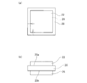
以下、本発明に係るパワーモジュール用基板およびその製造方法の実施形態について説明する。図1に、本発明に係るパワーモジュール用基板10に半導体素子12およびヒートシンク14が接合されてなるヒートシンク付パワーモジュール16を示す。
Hereinafter, embodiments of a power module substrate and a method for manufacturing the same according to the present invention will be described. FIG. 1 shows a
パワーモジュール用基板10は、セラミックス基板20と、セラミックス基板20の一方の面(表面)20aに接合されたアルミニウム回路層23(アルミニウム板22)と、このアルミニウム回路層23(アルミニウム板22)に接合された回路用銅板24と、セラミック基板20の他方の面(裏面)20bに接合されたアルミニウム放熱層27(放熱用アルミニウム板26)と、このアルミニウム放熱層27(放熱用アルミニウム板26)に接合された放熱用銅板28とを有する。
The
パワーモジュール用基板10は、セラミックス基板20にアルミニウム板22,放熱用アルミニウム板26を接合するアルミニウム板接合工程(図2)と、アルミニウム板22上および放熱用アルミニウム板26上に所望形状のレジスト層30,31を形成するレジスト形成工程と(図3)、セラミックス基板20上に接合されたアルミニウム板22,放熱用アルミニウム板26をエッチングして所望形状のアルミニウム回路層23,アルミニウム放熱層27を形成するエッチング工程(図4)と、回路用銅板24,放熱用銅板28を、アルミニウム回路層23,アルミニウム放熱層27の各上面にそれぞれ積層載置し、アルミニウム回路層23と回路用銅板24およびアルミニウム放熱層27と放熱用銅板28を固相拡散接合する銅板接合工程(図5)とを行うことにより製造される。
The
より具体的には、まず、図2に示すアルミニウム板接合工程において、絶縁層を形成するセラミックス基板20の表面20a,裏面20b上の所定位置に、半導体素子12が接合される回路層を形成する所定の大きさのアルミニウム板22およびヒートシンク14が接合される放熱層を形成する放熱用アルミニウム板26を面方向にはみ出さないように積層載置し、アルミニウム板22,放熱用アルミニウム板26の各下面全面をセラミックス基板20の表面20aおよび裏面20bにそれぞれ接合する。セラミックス基板20に対するアルミニウム板22,放熱用アルミニウム板26の位置決めは、例えば図2(a)に矢印で示すように、セラミックス基板20の2辺を基準とすることができる。
More specifically, first, in the aluminum plate bonding step shown in FIG. 2, a circuit layer to which the
セラミックス基板20は、回路層を形成するアルミニウム板22と放熱用アルミニウム板26との間の電気的接続を防止する絶縁材であって、例えばAlN(窒化アルミ),AlO3,Si3N4等で形成され、その板厚は0.2mm〜1.5mmである。アルミニウム板22,放熱用アルミニウム板26は例えば純度99.99%以上、板厚0.1mm〜1.0mmのアルミニウム圧延板である。これらのアルミニウム板22,放熱用アルミニウム板26とセラミックス基板20とを、例えばAl−Si系のろう材を用いて640℃〜650℃でろう付する。アルミニウム板22,放熱用アルミニウム板26の板厚を0.1mm以上とすることにより、応力緩衝効果を確保することができる。
The
次に、図3に示すレジスト形成工程において、セラミックス基板20上に接合されたアルミニウム板22上および放熱用アルミニウム板26上に、所望形状の回路パターンが得られるようにレジスト層30,31をそれぞれ形成する。レジスト層30,31は、例えばレジストインキをアルミニウム板22,放熱用アルミニウム板26の各表面にスクリーン印刷することにより形成される。
Next, in the resist forming step shown in FIG. 3, the resist
次に、図4に示すエッチング工程において、アルミニウム板22においてレジスト層30が接合されていない周辺部22a、および放熱用アルミニウム板26においてレジスト層31が接合されていない周辺部26aをエッチング処理により除去した後、レジスト層30,31を除去する。これにより所望形状の回路パターンを有するアルミニウム回路層23およびアルミニウム放熱層27が得られる。
Next, in the etching step shown in FIG. 4, the
図4において、エッチング処理により除去される周辺部22a,26aをハッチングおよび2点鎖線で示す。エッチング液としては、例えばアルミニウムに対して十分なエッチング性を有するFeCl3溶液を用いることができる。エッチング工程後のアルミニウム回路層23およびアルミニウム放熱層27の厚さを0.10mm以上とすることにより、パワーモジュール用基板10における応力緩衝効果を確保することができる。
In FIG. 4, the
次に、図5に示す銅板接合工程において、セラミックス基板20の表面20a上に接合されエッチングされたアルミニウム回路層23上の所定位置に、アルミニウム回路層23よりも大きい(アルミニウム回路層23の面積よりも大きい)所望の形状を有しアルミニウム回路層23とともに回路層を形成する回路用銅板24を、アルミニウム回路層23の上面全面を覆いかつセラミックス基板20上から面方向にはみ出さないように位置決めして積層載置する。同様に、セラミックス基板22の裏面20b上に接合されエッチングされたアルミニウム放熱層27上の所定位置に、アルミニウム放熱層27よりも大きい(アルミニウム放熱層27の面積よりも大きい)所望の形状を有しアルミニウム放熱層27とともに放熱層を形成する放熱用銅板28を、アルミニウム放熱層27の表面全面を覆いかつセラミックス基板20上から面方向にはみ出さないように位置決めして積層載置する。そして、銅とアルミニウムの共晶温度未満で加熱し、回路用銅板24とアルミニウム回路層23、および放熱用銅板28とアルミニウム放熱層27とをそれぞれ固相拡散接合する。
Next, in the copper plate bonding step shown in FIG. 5, the
回路用銅板24,放熱用銅板28は、例えば図5(a)に矢印で示すようにセラミックス基板20の2辺や、セラミックス基板20上に形成されたアルミニウム回路層23,アルミニウム放熱層27の2辺などを基準として位置決めすることができるが、いずれの場合もセラミックス基板20から面方向にはみ出さない状態とする。すなわち、回路用銅板24,放熱用銅板28及びアルミニウム回路層23,アルミニウム放熱層27はセラミックス基板20よりも小さい。
The
回路用銅板24,放熱用銅板28は、例えば接合前にプレス加工を行う等により、それぞれアルミニウム回路層23,アルミニウム放熱層27よりも大きい所望の形状に形成することができる。また、各部材の接合面は、固相拡散接合処理前に予め傷が除去されて平滑にされている。
The
回路用銅板24の寸法は、エッチング工程後の公差が最大となった場合であってもアルミニウム回路層23の全面を確実に覆うことができるように、エッチングの精度、回路用銅板24自体の寸法精度および配置精度を考慮して設定する。例えば、エッチングの精度が±0.25mmである場合、アルミニウム回路層23の基準寸法よりも回路用銅板24が0.25mm大きければ、アルミニウム回路層23の上面全面を覆うように回路用銅板24を接合することができる。さらに0.25mmの余裕を見込むと、アルミニウム回路層23が精度よく形成されている場合には、アルミニウム回路層23の外周縁23aと回路用銅板24の外周縁24aとの間の面方向寸法pが例えば1.0mm程度となる。
The size of the
同様に、アルミニウム放熱層27の表面全面を確実に覆うことができるように放熱用銅板28の寸法を設定すると、アルミニウム放熱層27が精度よく形成されている場合には、アルミニウム放熱層27の外周縁27aと放熱用銅板28の外周縁28aとの間の面方向寸法qが例えば1.0mm程度となる。
Similarly, when the dimensions of the heat
このように各部材の寸法を設定することにより、回路用銅板24よりも小さいアルミニウム回路層23の表面全面が回路用銅板24の裏面に固相拡散接合された状態となるとともに、放熱用銅板28よりも小さいアルミニウム放熱層27の表面全面が放熱用銅板28の裏面に固相拡散接合された状態となる。
By setting the dimensions of the respective members in this manner, the entire surface of the
回路用銅板24,放熱用銅板28は、0.05mm以上6.0mm以下の厚さを有する無酸素銅の圧延板であり、セラミックス基板20の表裏面に対して3kgf/cm2以上35kgf/cm2以下で加圧保持され、400℃以上548℃未満の加熱温度を5分以上240分以下保持する真空加熱により、それぞれアルミニウム回路層23,アルミニウム放熱層27に固相拡散接合される。なお、この銅板接合工程において、図5に2点鎖線で示すように、放熱用銅板28に対してさらにアルミニウムまたはアルミニウム合金製のヒートシンク14も同時に固相拡散接合してもよい。
The
回路用銅板24,放熱用銅板28の板厚を0.05mm以上とすることにより、半導体素子12からの熱を銅層24で拡げて熱をより効率的に伝達し、パワーサイクル負荷時の初期の熱抵抗を低減することができるので、パワーサイクルに対する信頼性をより高くすることができるとともに、アルミニウム回路層23,アルミニウム放熱層27からはみ出した部分の垂れ下がりを回避することができる。また、回路用銅板24,放熱用銅板28の板厚を6.0mm以下とすることにより、回路層および放熱層の剛性を低減させ、ヒートサイクル負荷時においてセラミックス基板20に割れが生じることを抑制できる。
By setting the thicknesses of the
固相拡散のための真空加熱における加熱温度は、アルミニウム板22(アルミニウム回路層23)を構成する金属(Al)と回路用銅板24を構成する金属(Cu)、放熱用アルミニウム板26(アルミニウム放熱層27)を構成する金属(Al)と放熱用銅板28を構成する金属(Cu)、ヒートシンク14も同時に接合する場合には放熱用銅板28を構成する金属(Cu)とヒートシンク14を構成する金属(例えばAl−Mg−Si系合金)の共晶温度のうち、最も低い共晶温度(共晶温度含まず)から共晶温度−5℃の範囲が好ましい。
The heating temperature in vacuum heating for solid phase diffusion is as follows: the metal (Al) constituting the aluminum plate 22 (aluminum circuit layer 23), the metal (Cu) constituting the
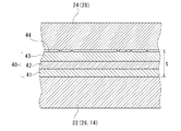
ここで、アルミニウム(アルミニウム板22、放熱用アルミニウム板26、ヒートシンク14)と銅(回路用銅板24、放熱用銅板28)との間における固相拡散接合について、アルミニウム板22と回路用銅板24との接合を例として図6を参照して説明する。アルミニウム板22と回路用銅板24とは、アルミニウム板22のアルミニウム原子と回路用銅板24の銅原子とが相互拡散することによって、拡散層40を形成して接合される。この拡散層40においては、アルミニウム板22から回路用銅板24に向かうにしたがい、漸次アルミニウム原子の濃度が低くなり、かつ銅原子の濃度が高くなる濃度勾配を有する。
Here, regarding solid phase diffusion bonding between aluminum (
拡散層40は、CuとAlとからなる金属間化合物で構成されており、本実施形態では図6に示すように、複数の金属間化合物が界面に沿って積層された構成となっている。拡散層40は、厚さtの平均が1μm以上80μm以下の範囲内、好ましくは、5μm以上80μm以下の範囲内に設定され、アルミニウム板22側から回路用銅板24側に向けて順にθ相41、η2相42、ζ2相43の3種の金属間化合物が積層されている。
The
なお、この拡散層は、アルミニウム板22側から銅板24側に向けて順に、前記接合界面に沿って、θ相、η2相が積層し、さらにζ2相、δ相、及びγ2相のうち少なくとも一つの相が積層した構造とされていても良い。
The diffusion layer is formed by laminating a θ phase and a η2 phase in order from the
さらに、回路用銅板24と固相拡散接合により形成された拡散層40との界面に沿って、酸化物44が層状に分散している。本実施形態においては、この酸化物44はアルミナ(Al2O3)等のアルミニウム酸化物である。酸化物44は、拡散層40と回路用銅板24との界面に分断された状態で分散しており、拡散層40と回路用銅板24とが直接接触している領域も存在する。なお、銅板24と拡散層40の界面に沿って、酸化物44が拡散層40の内部に層状に分散している構成とされても良い。本実施形態では、回路用銅板24の平均結晶粒径は50μm以上200μm以下の範囲内、アルミニウム板22の平均結晶粒径は500μm以上である。
Further,
以上説明したように、本実施形態に係る製造方法によれば、セラミックス基板20の表面20a上に設けたアルミニウム回路層23よりも大きな回路用銅板24を固相拡散接合により強固にアルミニウム回路層23に接合するので、銅層とアルミニウム層とが確実に接合されたパワーモジュール用基板10を得ることができる。
As described above, according to the manufacturing method according to the present embodiment, the
また、このように製造されたパワーモジュール用基板10においては、アルミニウム板22(アルミニウム回路層23)中のAlが回路用銅板24側へ、回路用銅板24中のCuがアルミニウム板22(アルミニウム回路層23)側へと十分に相互拡散し、アルミニウム板22(アルミニウム回路層23)と回路用銅板24との間に、CuとAlの拡散層40が形成されている。したがって、アルミニウム板22(アルミニウム回路層23)と回路用銅板24とが確実に固相拡散接合され、接合強度を確保することができる。
Further, in the
また、回路用銅板24と拡散層40との界面および放熱用銅板28と拡散層40との界面に沿って酸化物44が層状に分散しているので、アルミニウム板22(アルミニウム回路層23)および放熱用アルミニウム板26(アルミニウム放熱層27)に形成された酸化膜が確実に破壊され、CuとAlの相互拡散が十分に進行していることになり、回路用銅板24および放熱用銅板28と拡散層40とが確実に接合されている。
Since the
さらに、拡散層40において、複数の金属間化合物が接合界面に沿って積層されるので、脆い金属間化合物が大きく成長してしまうことが抑制されている。また、回路用銅板24中あるいは放熱用銅板28中のCuとアルミニウム板22(アルミニウム回路層23)中あるいは放熱用アルミニウム板26中のAlとが相互拡散することにより、回路用銅板24側あるいは放熱用銅板28側からアルミニウム板22(アルミニウム回路層23)側あるいは放熱用アルミニウム板26に向けてそれぞれの組成に適した金属間化合物が層状に形成されるので、接合界面の特性を安定させることができる。
Furthermore, since a plurality of intermetallic compounds are laminated along the bonding interface in the
具体的には、拡散層40は、アルミニウム板22(アルミニウム回路層23)側あるいは放熱用アルミニウム板26側から回路用銅板24側あるいは放熱用銅板28側に向けて順に、θ相41、η2相42、ζ2相43の3種の金属間化合物が積層又はθ相、η2相が積層し、さらにζ2相、δ相、及びγ2相のうち少なくとも一つの相が積層しているので、拡散層40内部における体積変動が小さく、内部歪みが抑えられる。
Specifically, the
また、アルミニウム板22(アルミニウム回路層23),放熱用アルミニウム板26および回路用銅板24,放熱用銅板28の平均結晶粒径が比較的大きく、アルミニウム板22(アルミニウム回路層23),放熱用アルミニウム板26の平均結晶粒径が500μm以上、回路用銅板24,放熱用銅板28の平均結晶粒径が50μm以上200μm以下の範囲内に設定されている。これにより、アルミニウム板22(アルミニウム回路層23)および回路用銅板24あるいは放熱用アルミニウム板26放熱用銅板28に過剰な歪み等が蓄積されず、疲労特性が向上する。したがって、ヒートサイクル負荷において、パワーモジュール用基板10とヒートシンク14との間に生じる熱応力に対する接合信頼性が向上する。
The average crystal grain size of the aluminum plate 22 (aluminum circuit layer 23), the heat
さらに、拡散層40の平均厚さtが1μm以上80μm以下、好ましくは5μm以上80μm以下の範囲内であることにより、CuとAlとの相互拡散が十分に進行しており、アルミニウム板22(アルミニウム回路層23)と回路用銅板24および放熱用アルミニウム板26(アルミニウム放熱層27)と放熱用銅板28を強固に接合できるとともに、アルミニウム板22(アルミニウム回路層23),放熱用アルミニウム板26(アルミニウム放熱層27)および回路用銅板24,放熱用銅板28に比べて脆い金属間化合物が必要以上に成長することが抑えられ、接合界面の特性が安定する。
Furthermore, when the average thickness t of the
なお、上記実施形態では、純度99.99%のアルミニウム板を用いたが、これに限らず、純度99%又は純度99.9%のアルミニウム板やアルミニウム合金からなる板を用いることもできる。また、無酸素銅からなる銅板を用いたが、これに限らず、他の純銅からなる銅板又は銅合金からなる銅板を用いることもできる。 In the above embodiment, an aluminum plate having a purity of 99.99% is used. However, the present invention is not limited to this, and an aluminum plate having a purity of 99% or 99.9% or a plate made of an aluminum alloy can also be used. Moreover, although the copper plate which consists of oxygen-free copper was used, it is not restricted to this, The copper plate which consists of another pure copper or the copper plate which consists of copper alloys can also be used.
また、上記実施形態ではエッチングによって所望形状の回路パターンを有するアルミニウム回路層23を形成したが、プレス加工により所望形状の回路パターンを有するアルミニウム板を作成し、このアルミニウム板をセラミックス基板に接合することで、所望形状の回路パターンを有するアルミニウム回路層を形成することもできる。
Moreover, in the said embodiment, although the
以上説明したように、本発明のパワーモジュール用基板の製造方法によれば、セラミックス基板上に複数の金属層が積層されるパワーモジュール用基板において、各層間を確実に接合できるとともに、所望の回路パターンを高い寸法精度で確実に形成できるので、搭載された半導体素子からの放熱性を向上させ、パワーモジュール用基板の小型が実現できる。 As described above, according to the method for manufacturing a power module substrate of the present invention, in a power module substrate in which a plurality of metal layers are laminated on a ceramic substrate, each layer can be reliably bonded and a desired circuit can be obtained. Since the pattern can be reliably formed with high dimensional accuracy, the heat dissipation from the mounted semiconductor element can be improved, and the power module substrate can be miniaturized.
また、本発明のパワーモジュール用基板によれば、半導体素子の発熱を効率よく放散でき、銅板およびアルミニウム回路層の温度上昇が抑制されるので、ヒートサイクルによる負荷に対する信頼性を向上できる。 Further, according to the power module substrate of the present invention, the heat generation of the semiconductor element can be efficiently dissipated and the temperature rise of the copper plate and the aluminum circuit layer is suppressed, so that the reliability with respect to the load caused by the heat cycle can be improved.
なお、本発明は前記実施形態の構成のものに限定されるものではなく、細部構成においては、本発明の趣旨を逸脱しない範囲において種々の変更を加えることが可能である。例えば放熱層は、前記実施形態のように銅板を含む構成と、銅板を含まずアルミニウム板のみで形成する構成と、いずれの形態であってもよい。 In addition, this invention is not limited to the thing of the structure of the said embodiment, In a detailed structure, it is possible to add a various change in the range which does not deviate from the meaning of this invention. For example, the heat dissipation layer may have either a configuration including a copper plate as in the above-described embodiment, or a configuration including only an aluminum plate without including a copper plate.
10 パワーモジュール用基板
12 半導体素子
14 ヒートシンク
16 ヒートシンク付パワーモジュール
20 セラミックス基板(絶縁層)
20a 表面
20b 裏面
22 アルミニウム板
22a 周辺部
23 アルミニウム回路層
23a 外周縁
24 回路用銅板(回路層)
24a 外周縁
26 放熱用アルミニウム板
26a 周辺部
27 アルミニウム放熱層
27a 外周縁
28 放熱用銅板(放熱層)
28a 外周縁
30,31 レジスト層
40 拡散層
41 θ相
42 η2相
43 ζ2相
44 酸化物
DESCRIPTION OF
24a outer
28a Outer
Claims (6)
前記セラミックス基板よりも小さい回路形状を有し、前記セラミックス基板の表面上の所定位置に積層状態で下面全面を接合されたアルミニウム回路層と、
前記セラミックス基板に接合された前記アルミニウム回路層よりも大きく、前記セラミックス基板よりも小さく、前記セラミックス基板から面方向にはみ出さない状態で前記アルミニウム回路層の上面全面を覆うように接合された銅板と
を有することを特徴とするパワーモジュール用基板。 A ceramic substrate;
An aluminum circuit layer having a circuit shape smaller than that of the ceramic substrate, and bonded to the entire lower surface in a laminated state at a predetermined position on the surface of the ceramic substrate;
A copper plate that is larger than the aluminum circuit layer bonded to the ceramic substrate, smaller than the ceramic substrate, and bonded so as to cover the entire upper surface of the aluminum circuit layer in a state that does not protrude from the ceramic substrate in the plane direction; A power module substrate comprising:
絶縁層を形成するセラミックス基板の表面上の所定位置に、回路層を形成する所定の大きさのアルミニウム板を面方向にはみ出さないように積層載置し、前記セラミックス基板の前記表面に前記アルミニウム板の下面全面を接合するアルミニウム板接合工程と、
前記アルミニウム板上にジスト層を形成するレジスト形成工程と、
前記セラミックス基板上に接合された前記アルミニウム板をエッチングしてアルミニウム回路層を形成するエッチング工程と、
前記アルミニウム回路層よりも大きく前記セラミックス基板よりも小さい銅板を、前記アルミニウム回路層の上面全面を覆いかつ前記セラミックス基板上から面方向にはみ出さないように積層載置し、銅とアルミニウムの共晶温度未満で加熱し前記アルミニウム回路層と前記銅板とを固相拡散接合する銅板接合工程と、
を有することを特徴とするパワーモジュール用基板の製造方法。 A method for manufacturing a power module substrate having an insulating layer and a circuit layer formed on one surface of the insulating layer,
An aluminum plate having a predetermined size for forming the circuit layer is stacked and placed at a predetermined position on the surface of the ceramic substrate on which the insulating layer is formed so as not to protrude in the plane direction, and the aluminum is formed on the surface of the ceramic substrate. An aluminum plate joining process for joining the entire lower surface of the plate;
Forming a resist layer on the aluminum plate;
An etching step of etching the aluminum plate bonded onto the ceramic substrate to form an aluminum circuit layer;
A copper plate that is larger than the aluminum circuit layer and smaller than the ceramic substrate is stacked and placed so as to cover the entire upper surface of the aluminum circuit layer and not protrude in the plane direction from the ceramic substrate. A copper plate joining step of heating the aluminum circuit layer below the temperature and solid-phase diffusion joining the copper circuit layer and the copper plate;
The manufacturing method of the board | substrate for power modules characterized by having.
前記銅板接合工程において、前記セラミックス基板上に接合された前記放熱用アルミニウム板上の所定位置に、放熱用銅板を位置決めして積層載置し、前記放熱用アルミニウム板と前記放熱用銅板とを固相拡散接合することにより、
前記絶縁層の他方の面に、前記放熱用アルミニウム板および前記放熱用銅板が積層されてなる放熱層を形成することを特徴とする請求項5に記載のパワーモジュール用基板の製造方法。 In the aluminum plate joining step, a heat dissipation aluminum plate having a predetermined size for forming a heat dissipation layer is positioned and stacked at a predetermined position on the back surface of the ceramic substrate, and the heat dissipation aluminum plate is placed on the aluminum plate. Together with the ceramic substrate,
In the copper plate joining step, the heat radiating copper plate is positioned and placed at a predetermined position on the heat radiating aluminum plate joined to the ceramic substrate, and the heat radiating aluminum plate and the heat radiating copper plate are fixed. By phase diffusion bonding,
6. The method for manufacturing a power module substrate according to claim 5, wherein a heat radiating layer formed by laminating the heat radiating aluminum plate and the heat radiating copper plate is formed on the other surface of the insulating layer.
Priority Applications (1)
| Application Number | Priority Date | Filing Date | Title |
|---|---|---|---|
| JP2013202001A JP6149655B2 (en) | 2013-09-27 | 2013-09-27 | Power module substrate and manufacturing method thereof |
Applications Claiming Priority (1)
| Application Number | Priority Date | Filing Date | Title |
|---|---|---|---|
| JP2013202001A JP6149655B2 (en) | 2013-09-27 | 2013-09-27 | Power module substrate and manufacturing method thereof |
Publications (2)
| Publication Number | Publication Date |
|---|---|
| JP2015070062A JP2015070062A (en) | 2015-04-13 |
| JP6149655B2 true JP6149655B2 (en) | 2017-06-21 |
Family
ID=52836480
Family Applications (1)
| Application Number | Title | Priority Date | Filing Date |
|---|---|---|---|
| JP2013202001A Active JP6149655B2 (en) | 2013-09-27 | 2013-09-27 | Power module substrate and manufacturing method thereof |
Country Status (1)
| Country | Link |
|---|---|
| JP (1) | JP6149655B2 (en) |
Family Cites Families (5)
| Publication number | Priority date | Publication date | Assignee | Title |
|---|---|---|---|---|
| JPH09234826A (en) * | 1995-12-28 | 1997-09-09 | Dowa Mining Co Ltd | Metal-ceramic composite base plate and manufacture thereof |
| JP3012835B2 (en) * | 1997-11-07 | 2000-02-28 | 電気化学工業株式会社 | Substrate and its manufacturing method, metal joined body suitable for substrate |
| JP3797784B2 (en) * | 1998-03-13 | 2006-07-19 | 電気化学工業株式会社 | Circuit board |
| JP2001102703A (en) * | 1999-10-01 | 2001-04-13 | Denki Kagaku Kogyo Kk | Circuit board |
| JP2002373955A (en) * | 2001-06-13 | 2002-12-26 | Sumitomo Metal Electronics Devices Inc | Power module substrate |
-
2013
- 2013-09-27 JP JP2013202001A patent/JP6149655B2/en active Active
Also Published As
| Publication number | Publication date |
|---|---|
| JP2015070062A (en) | 2015-04-13 |
Similar Documents
| Publication | Publication Date | Title |
|---|---|---|
| JP6488917B2 (en) | Power module substrate with heat sink and power module | |
| JP5892281B2 (en) | Power module substrate with heat sink and power module | |
| JP6171622B2 (en) | Power module substrate, power module, and method of manufacturing power module substrate | |
| TWI690041B (en) | Substrate for power module with heat sink and power module | |
| WO2014115677A1 (en) | Power module substrate, power module substrate with heat sink, and power module with heat sink | |
| JP6146242B2 (en) | Power module substrate manufacturing method | |
| JP5067187B2 (en) | Power module substrate with heat sink and power module with heat sink | |
| JP6417834B2 (en) | Power module substrate with cooler and method for manufacturing power module substrate with cooler | |
| JP2008235852A (en) | Ceramic substrate and semiconductor module using the same | |
| JP6330951B2 (en) | Joints for manufacturing power module substrates | |
| JP6149654B2 (en) | Power module substrate manufacturing method | |
| JP5987418B2 (en) | Manufacturing method of power module substrate with heat sink | |
| WO2019189329A1 (en) | Insulated circuit board with heat sink | |
| JP6183166B2 (en) | Power module substrate with heat sink and manufacturing method thereof | |
| JP6020256B2 (en) | Manufacturing method of power module substrate with heat sink | |
| JP2010238965A (en) | Substrate for power module, method for manufacturing substrate for power module, and power module | |
| JP6149655B2 (en) | Power module substrate and manufacturing method thereof | |
| JP6638284B2 (en) | Substrate for power module with heat sink and power module | |
| JP6565735B2 (en) | Power module substrate, power module, and method of manufacturing power module substrate | |
| JP2010238963A (en) | Substrate for power module, method for manufacturing substrate for power module, and power module | |
| TWI762771B (en) | Insulated circuit board | |
| JP2013211288A (en) | Manufacturing method of substrate for power module with heat sink | |
| JP6201297B2 (en) | Power module substrate with copper plate and method for manufacturing power module substrate with copper plate | |
| JP6237058B2 (en) | Power module substrate with copper plate and method for manufacturing power module substrate with copper plate | |
| JP6127852B2 (en) | Power module substrate with heat sink and manufacturing method thereof |
Legal Events
| Date | Code | Title | Description |
|---|---|---|---|
| A621 | Written request for application examination |
Free format text: JAPANESE INTERMEDIATE CODE: A621 Effective date: 20160331 |
|
| A977 | Report on retrieval |
Free format text: JAPANESE INTERMEDIATE CODE: A971007 Effective date: 20170322 |
|
| TRDD | Decision of grant or rejection written | ||
| A01 | Written decision to grant a patent or to grant a registration (utility model) |
Free format text: JAPANESE INTERMEDIATE CODE: A01 Effective date: 20170425 |
|
| A61 | First payment of annual fees (during grant procedure) |
Free format text: JAPANESE INTERMEDIATE CODE: A61 Effective date: 20170508 |
|
| R150 | Certificate of patent or registration of utility model |
Ref document number: 6149655 Country of ref document: JP Free format text: JAPANESE INTERMEDIATE CODE: R150 |