JP2017228551A - Metal-ceramic combining substrate and manufacturing method thereof - Google Patents
Metal-ceramic combining substrate and manufacturing method thereof Download PDFInfo
- Publication number
- JP2017228551A JP2017228551A JP2016121344A JP2016121344A JP2017228551A JP 2017228551 A JP2017228551 A JP 2017228551A JP 2016121344 A JP2016121344 A JP 2016121344A JP 2016121344 A JP2016121344 A JP 2016121344A JP 2017228551 A JP2017228551 A JP 2017228551A
- Authority
- JP
- Japan
- Prior art keywords
- metal
- ceramic
- substrate
- base plate
- ceramic substrate
- Prior art date
- Legal status (The legal status is an assumption and is not a legal conclusion. Google has not performed a legal analysis and makes no representation as to the accuracy of the status listed.)
- Granted
Links
Images


Landscapes
- Cooling Or The Like Of Semiconductors Or Solid State Devices (AREA)
Abstract
【課題】アルミニウムまたはアルミニウム合金からなるベース板がセラミックス基板に直接接合した金属−セラミックス接合基板において、半導体チップなどを半田付けする際などの加熱によるベース板の反りのばらつきを抑制することができる、金属−セラミックス接合基板およびその製造方法を提供する。【解決手段】金属−セラミックス接合基板は、平面形状が略矩形のセラミックス基板10と、このセラミックス基板10の一方の面(回路パターン側の面)の周縁部と側面および他方の面(裏面)の全面に直接接合した平面形状が略矩形のアルミニウムまたはアルミニウム合金からなるベース板12と、セラミックス基板10の一方の面の周縁部に直接接合したベース板12から離間してセラミックス基板10の一方の面に直接接合したアルミニウムまたはアルミニウム合金からなる回路パターン用金属板14とを備えている。【選択図】図1CKind Code: A1 A metal-ceramic bonded substrate in which a base plate made of aluminum or an aluminum alloy is directly bonded to a ceramic substrate is capable of suppressing variations in warping of the base plate due to heating when a semiconductor chip or the like is soldered. A metal-ceramic bonded substrate and a method for manufacturing the same are provided. A metal-ceramic bonding substrate includes a ceramic substrate 10 having a substantially rectangular planar shape, and a peripheral edge portion and a side surface of one surface (surface on the circuit pattern side) of the ceramic substrate 10 and the other surface (back surface). A base plate 12 made of aluminum or an aluminum alloy having a substantially rectangular planar shape directly bonded to the entire surface, and one surface of the ceramics substrate 10 spaced apart from the base plate 12 directly bonded to the peripheral edge portion of one surface of the ceramics substrate 10. and a circuit pattern metal plate 14 made of aluminum or an aluminum alloy directly bonded to the substrate. [Selection drawing] Fig. 1C
Description
本発明は、金属−セラミックス接合基板およびその製造方法に関し、特に、金属部材がセラミックス基板に接合した金属−セラミックス接合基板およびその製造方法に関する。 The present invention relates to a metal / ceramic bonding substrate and a manufacturing method thereof, and more particularly to a metal / ceramic bonding substrate in which a metal member is bonded to a ceramic substrate and a manufacturing method thereof.
電気自動車、電車、工作機械などの大電流を制御するために使用される従来のパワーモジュールでは、ベース板と呼ばれる金属板または複合材の一方の面に金属−セラミックス絶縁基板が半田付けにより固定されるとともに、この金属−セラミックス絶縁基板上に半導体チップが半田付けにより固定され、ベース板の他方の面(裏面)に熱伝導グリースを介してねじ止めなどにより金属製の放熱フィンや冷却ジャケットが取り付けられている。 In conventional power modules used to control large currents in electric vehicles, trains, machine tools, etc., a metal-ceramic insulating substrate is fixed to one side of a metal plate or composite material called a base plate by soldering. At the same time, a semiconductor chip is fixed on the metal-ceramic insulating substrate by soldering, and a metal radiating fin or cooling jacket is attached to the other surface (back surface) of the base plate by screwing it with thermal grease. It has been.
この金属−セラミックス絶縁基板へのベース板や半導体チップの半田付けは加熱により行われるため、半田付けの際に接合部材間の熱膨張係数の差によりベース板の反りが生じ易い。また、半導体チップから発生した熱は、金属−セラミックス絶縁基板と半田とベース板を介して放熱フィンや冷却ジャケットにより空気や冷却水に逃がされるため、半田付けの際にベース板の反りが生じると、放熱フィンや冷却ジャケットをベース板に取り付けたときのクリアランスが大きくなり、放熱性が極端に低下する。 Since the base plate and the semiconductor chip are soldered to the metal-ceramic insulating substrate by heating, the base plate is likely to warp due to the difference in thermal expansion coefficient between the joining members during soldering. Also, the heat generated from the semiconductor chip is released to the air and cooling water by the heat radiation fins and the cooling jacket through the metal-ceramic insulating substrate, the solder, and the base plate, so that the base plate warps during soldering. , The clearance when radiating fins and cooling jackets are attached to the base plate is increased, and the heat dissipation is extremely reduced.
このような問題を解消して、金属−セラミックス絶縁基板の信頼性を高めるため、降伏応力が非常に低いアルミニウムをベース板に使用した金属−セラミックス回路基板、例えば、耐力が320MPa以下であり且つ厚さが1mm以上のアルミニウムまたはアルミニウム合金からなるベース板を溶湯法によってセラミックス基板に直接接合した金属−セラミックス回路基板が提案されている(例えば、特許文献1参照)。 In order to solve such problems and increase the reliability of the metal-ceramic insulating substrate, a metal-ceramic circuit substrate using aluminum having a very low yield stress as a base plate, for example, having a proof stress of 320 MPa or less and a thickness A metal-ceramic circuit board has been proposed in which a base plate made of aluminum or aluminum alloy having a length of 1 mm or more is directly bonded to a ceramic substrate by a molten metal method (see, for example, Patent Document 1).
しかし、アルミニウムの降伏応力を小さくするためにはアルミニウムの純度を高くする必要があるが、溶湯法ではアルミニウムの結晶粒径を制御し難く、10mm以上の大きな結晶粒径しか得ることができない。このように結晶粒径が大きいと、結晶粒度分布にばらつきが起こり、半導体チップなどを半田付けする際などの加熱によるアルミニウムベース板の反りにばらつきがある。 However, in order to reduce the yield stress of aluminum, it is necessary to increase the purity of aluminum. However, in the molten metal method, it is difficult to control the crystal grain size of aluminum, and only a large crystal grain size of 10 mm or more can be obtained. When the crystal grain size is large in this way, the crystal grain size distribution varies, and the warp of the aluminum base plate due to heating when soldering a semiconductor chip or the like varies.
したがって、本発明は、このような従来の問題点に鑑み、アルミニウムまたはアルミニウム合金からなるベース板がセラミックス基板に直接接合した金属−セラミックス接合基板において、半導体チップなどを半田付けする際などの加熱によるベース板の反りのばらつきを抑制することができる、金属−セラミックス接合基板およびその製造方法を提供することを目的とする。 Therefore, in view of such a conventional problem, the present invention is based on heating when soldering a semiconductor chip or the like in a metal-ceramic bonding substrate in which a base plate made of aluminum or an aluminum alloy is directly bonded to a ceramic substrate. An object of the present invention is to provide a metal / ceramic bonding substrate and a method for manufacturing the same, which can suppress variations in warpage of the base plate.
本発明者らは、上記課題を解決するために鋭意研究した結果、鋳型内にセラミックス基板を配置し、このセラミックス基板の両面の所定の部分に接触するようにアルミニウムまたはアルミニウム合金の溶湯を注湯した後に溶湯を冷却して固化させることにより、アルミニウムまたはアルミニウム合金からなるベース板をセラミックス基板の一方の面の周縁部と側面および他方の面の全面に形成してセラミックス基板に直接接合させるとともに、アルミニウムまたはアルミニウム合金からなる回路パターン用金属板をベース板から離間してセラミックス基板の一方の面に形成してセラミックス基板に直接接合させることによって、半導体チップなどを半田付けする際などの加熱によるベース板の反りのばらつきを抑制することができることを見出し、本発明を完成するに至った。 As a result of diligent research to solve the above problems, the present inventors have arranged a ceramic substrate in a mold and poured molten aluminum or aluminum alloy so as to contact predetermined portions on both sides of the ceramic substrate. Then, by cooling and solidifying the molten metal, a base plate made of aluminum or an aluminum alloy is formed on the peripheral portion of one surface of the ceramic substrate and the entire surface of the other surface and directly bonded to the ceramic substrate, A base by heating such as when soldering a semiconductor chip, etc. by forming a metal plate for circuit pattern made of aluminum or aluminum alloy on one surface of the ceramic substrate apart from the base plate and directly bonding it to the ceramic substrate It can be seen that variations in warping of the plate can be suppressed. And it has led to the completion of the present invention.
すなわち、本発明による金属−セラミックス接合基板の製造方法は、鋳型内にセラミックス基板を配置し、このセラミックス基板の両面の所定の部分に接触するようにアルミニウムまたはアルミニウム合金の溶湯を注湯した後に溶湯を冷却して固化させることにより、アルミニウムまたはアルミニウム合金からなるベース板をセラミックス基板の一方の面の周縁部と側面および他方の面の全面に形成してセラミックス基板に直接接合させるとともに、アルミニウムまたはアルミニウム合金からなる回路パターン用金属板をベース板から離間してセラミックス基板の一方の面に形成してセラミックス基板に直接接合させることを特徴とする。 That is, in the method for manufacturing a metal / ceramic bonding substrate according to the present invention, a ceramic substrate is placed in a mold, and a molten metal of aluminum or an aluminum alloy is poured so as to come into contact with predetermined portions on both surfaces of the ceramic substrate. Is cooled and solidified to form a base plate made of aluminum or an aluminum alloy on the periphery and side surfaces of one surface of the ceramic substrate and the entire surface of the other surface and directly bonded to the ceramic substrate. A circuit pattern metal plate made of an alloy is formed on one surface of a ceramic substrate at a distance from the base plate and directly bonded to the ceramic substrate.
この金属−セラミックス接合基板の製造方法において、鋳型内にセラミックス基板を配置する際に、鋳型内にセラミックス基板と強化部材とを互いに離間して配置し、溶湯を注湯する際に、鋳型内の強化部材の全面に溶湯を接触させ、ベース板を形成してセラミックス基板に直接接合させる際に、鋳型内の強化部材がベース板に取り囲まれるように強化部材をベース板に直接接合させてもよい。この場合、強化部材は、ベース板の材料より融点が高い金属またはセラミックス材料からなるのが好ましい。また、鋳型が上側鋳型部材と下側鋳型部材とからなり、強化部材の端部が上側鋳型部材と下側部材に挟持されて強化部材が鋳型に支持され、下側鋳型部材の底面から突出して形成された複数の基板支持部にセラミックス基板の端部の底面および側面が当接して支持され、複数の基板支持部の少なくとも一つのセラミックス基板の端部の側面に当接する部分の上面が、複数の基板支持部に支持されたセラミックス基板の上面より高くなっているのが好ましい。 In this method of manufacturing a metal / ceramic bonding substrate, when placing a ceramic substrate in the mold, the ceramic substrate and the reinforcing member are spaced apart from each other in the mold, and when pouring the molten metal, When the molten metal is brought into contact with the entire surface of the reinforcing member and the base plate is formed and directly bonded to the ceramic substrate, the reinforcing member may be directly bonded to the base plate so that the reinforcing member in the mold is surrounded by the base plate. . In this case, the reinforcing member is preferably made of a metal or ceramic material having a melting point higher than that of the base plate material. Further, the mold is composed of an upper mold member and a lower mold member, the end of the reinforcing member is sandwiched between the upper mold member and the lower member, the reinforcing member is supported by the mold, and protrudes from the bottom surface of the lower mold member. The bottom surface and the side surface of the end portion of the ceramic substrate are in contact with and supported by the plurality of formed substrate support portions, and the top surface of the portion that contacts the side surface of the end portion of at least one ceramic substrate of the plurality of substrate support portions is plural. It is preferable that the height is higher than the upper surface of the ceramic substrate supported by the substrate support portion.
また、鋳型内にセラミックス基板を配置する際に、鋳型内にセラミックス基板と電子部品とを互いに離間して配置し、溶湯を注湯する際に、電子部品の一方の面に溶湯を接触させ、回路パターン用金属板を形成してセラミックス基板に直接接合させる際に、回路パターン用金属板に電子部品を直接接合させてもよい。また、ベース板を形成してセラミックス基板に直接接合させる際に、ベース板の回路パターン用金属板と反対側の面に、互いに略平行に且つ一定の間隔で離間して配置された複数の板状フィンをベース板と一体に形成してもよい。あるいは、ベース板を形成してセラミックス基板に直接接合させる際に、ベース板の回路パターン用金属板と反対側の面に、互いに離間して突出する多数の柱状突起部をベース板と一体に形成してもよい。また、ベース板および回路パターン用金属板をセラミックス基板に直接接合させた後、回路パターン用金属板の不要部分をエッチングにより除去して所望の回路パターンを形成することができる。 Further, when placing the ceramic substrate in the mold, the ceramic substrate and the electronic component are arranged apart from each other in the mold, and when pouring the molten metal, the molten metal is brought into contact with one surface of the electronic component, When the circuit pattern metal plate is formed and directly bonded to the ceramic substrate, the electronic component may be directly bonded to the circuit pattern metal plate. In addition, when the base plate is formed and directly bonded to the ceramic substrate, a plurality of plates arranged on the surface of the base plate opposite to the circuit pattern metal plate substantially parallel to each other and spaced apart from each other by a predetermined interval The fins may be formed integrally with the base plate. Alternatively, when the base plate is formed and bonded directly to the ceramic substrate, a large number of columnar protrusions that protrude away from each other are formed integrally with the base plate on the surface of the base plate opposite to the circuit pattern metal plate. May be. Further, after the base plate and the circuit pattern metal plate are directly bonded to the ceramic substrate, unnecessary portions of the circuit pattern metal plate can be removed by etching to form a desired circuit pattern.
また、本発明による金属−セラミックス接合基板は、セラミックス基板と、このセラミックス基板の一方の面の周縁部と側面および他方の面の全面に直接接合したアルミニウムまたはアルミニウム合金からなるベース板と、このベース板から離間してセラミックス基板の一方の面に直接接合したアルミニウムまたはアルミニウム合金からなる回路パターン用金属板とを備えたことを特徴とする。 A metal-ceramic bonding substrate according to the present invention includes a ceramic substrate, a base plate made of aluminum or an aluminum alloy directly bonded to the peripheral portion and side surface of one surface of the ceramic substrate, and the entire surface of the other surface, and the base. And a circuit pattern metal plate made of aluminum or an aluminum alloy, which is separated from the plate and directly bonded to one surface of the ceramic substrate.
この金属−セラミックス接合基板において、ベース板の内部に、板状の強化部材が、セラミックス基板から離間して且つセラミックス基板と略平行に配置して、ベース板に直接接合してもよい。この場合、強化部材は、ベース板の材料より融点が高い金属またはセラミックス材料からなるのが好ましい。また、回路パターン用金属板のセラミックス基板と反対側の面に、電子部品が直接接合してもよい。また、ベース板のセラミックス基板と反対側の面に、複数の板状フィンを、互いに略平行に且つ一定の間隔で離間して配置して、ベース板と一体に形成してもよい。さらに、ベース板のセラミックス基板と反対側の面に、互いに離間して突出する多数の柱状突起部を、ベース板と一体に形成してもよい。また、ベース板のセラミックス基板の側面に隣接した部分に、セラミックス基板の厚さより深い凹部を形成してもよい。 In this metal / ceramic bonding substrate, a plate-like reinforcing member may be disposed inside the base plate so as to be spaced apart from the ceramic substrate and substantially parallel to the ceramic substrate and directly bonded to the base plate. In this case, the reinforcing member is preferably made of a metal or ceramic material having a melting point higher than that of the base plate material. Further, the electronic component may be directly joined to the surface of the circuit pattern metal plate opposite to the ceramic substrate. In addition, a plurality of plate-like fins may be arranged on the surface of the base plate opposite to the ceramic substrate so as to be substantially parallel to each other and spaced apart from each other by a predetermined interval, and formed integrally with the base plate. Furthermore, a large number of columnar protrusions that protrude away from each other may be formed integrally with the base plate on the surface of the base plate opposite to the ceramic substrate. Moreover, you may form a recessed part deeper than the thickness of a ceramic substrate in the part adjacent to the side surface of the ceramic substrate of a base board.
本発明によれば、アルミニウムまたはアルミニウム合金からなるベース板がセラミックス基板に直接接合した金属−セラミックス接合基板において、半導体チップなどを半田付けする際などの加熱によるベース板の反りのばらつきを抑制することができる。 According to the present invention, in a metal-ceramic bonding substrate in which a base plate made of aluminum or an aluminum alloy is directly bonded to a ceramic substrate, variation in warpage of the base plate due to heating when soldering a semiconductor chip or the like is suppressed. Can do.
以下、添付図面を参照して、本発明による金属−セラミックス接合基板の実施の形態について詳細に説明する。 Embodiments of a metal / ceramic bonding substrate according to the present invention will be described below in detail with reference to the accompanying drawings.
[第1の実施の形態]
図1A〜図1Cは、本発明による金属−セラミックス接合基板の第1の実施の形態を示し、図2および図3A〜図3Eは、その金属−セラミックス接合基板を製造するために使用する鋳型を示している。
[First Embodiment]
1A to 1C show a first embodiment of a metal / ceramic bonding substrate according to the present invention, and FIGS. 2 and 3A to 3E show molds used for manufacturing the metal / ceramic bonding substrate. Show.
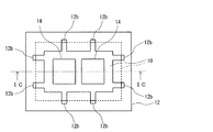
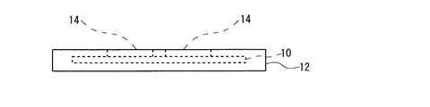
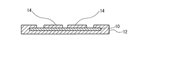
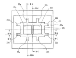
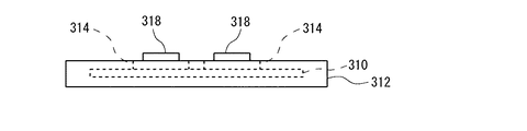
図1A〜図1Cに示すように、本発明による金属−セラミックス接合基板の第1の実施の形態は、平面形状が略矩形のセラミックス基板10と、このセラミックス基板10の一方の面(回路パターン側の面)の周縁部と側面および他方の面(裏面)の全面に直接接合した平面形状が略矩形のアルミニウムまたはアルミニウム合金からなるベース板12と、セラミックス基板10の一方の面の周縁部に直接接合したベース板12から離間してセラミックス基板10の一方の面に直接接合したアルミニウムまたはアルミニウム合金からなる1以上(図示した実施の形態では2つ)の回路パターン用金属板14とを備えている。
As shown in FIGS. 1A to 1C, the first embodiment of the metal / ceramic bonding substrate according to the present invention includes a
本実施の形態の金属−セラミックス接合基板は、図2に示すような鋳型20内にセラミックス基板10を配置し、セラックス基板10の両面のベース板12と回路パターン用金属板14に対応する部分に接触するように、アルミニウムまたはアルミニウム合金の溶湯を流し込んで冷却することによって製造することができる。
In the metal / ceramic bonding substrate of the present embodiment, the
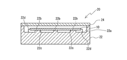
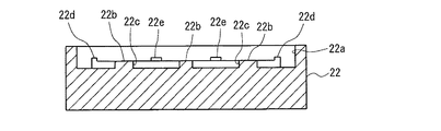
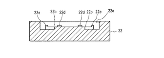
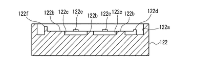
図2に示すように、鋳型20は、(多孔質の)カーボンまたは多孔質金属などの(溶湯不透過の)通気性材料からなり、それぞれ平面形状が略矩形の下側鋳型部材22と上側鋳型部材24とから構成されている。
As shown in FIG. 2, the
図2および図3A〜図3Eに示すように、下側鋳型部材22の上面には、ベース板を形成するための凹部(ベース板形成部)22aが形成されている。
As shown in FIG. 2 and FIGS. 3A to 3E, a recess (base plate forming portion) 22 a for forming a base plate is formed on the upper surface of the
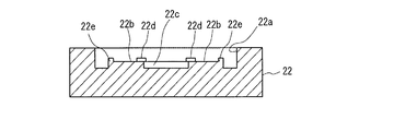
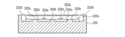
このベース板形成部22aの底面の略中央部には、この底面から略垂直方向に隆起した平面形状が略矩形の隆起部22bが形成されている。この隆起部22bの上面の略中央部には、回路パターン用金属板を形成するための1以上(図示した実施の形態では2つ)の凹部(回路パターン用金属板形成部)22cが形成されている。この回路パターン用金属板形成部22cは、隆起部22bを介してベース板形成部22aから離間しており、ベース板12(の回路パターン側の部分)と回路パターン用金属板14との間の絶縁を確保するようになっている。
A raised
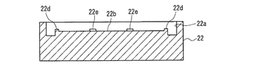
また、ベース板形成部22aの底面には、セラミックス基板10の長手方向両端部を支持する平面形状が略矩形の複数(図示した実施の形態では2対)の基板支持部(長手方向基板支持部)22dと、セラミックス基板10の幅方向両端部を支持する平面形状が略矩形の複数(図示した実施の形態では2対)の基板支持部(幅方向基板支持部)22eが、その底面から略垂直方向に突出して形成されている。これらの基板支持部22dおよび22eは、セラミックス基板10の一方の面(回路パターン側の面)の周縁部と側面に当接してセラミックス基板10を所定の位置で支持するために、それぞれ略L字型の断面を有するように段差が設けられている。これらの基板支持部22dおよび22e上にセラミックス基板10を配置すると、ベース板形成部22aの底面の略中央部に形成された隆起部22bの上面にセラミックス基板10が当接して載置されるようになっている。このようにセラミックス基板10を隆起部22bの上面に載置すると、セラミックス基板10によって回路パターン用金属板形成部22cの開口部が塞がれるとともに、セラミックス基板10の一方の面(回路パターン側の面)の周縁部と側面および他方の面(裏面)の全面の周囲にベース板形成部22aが確保されるようになっている。
Further, on the bottom surface of the base
なお、上側鋳型部材24には、(図示しない)注湯ノズルから下側鋳型部材22のベース板形成部22a内に溶湯を注湯するための(図示しない)注湯口が形成されているとともに、下側鋳型部材22には、ベース板形成部22aと回路パターン用金属板形成部22cとの間に延びる(図示しない)溶湯流路が形成されて、セラミックス基板10を隆起部22bの上面に載置したときにもベース板形成部22aと回路パターン用金属板形成部22cとの間が連通するようになっている。
The
このような鋳型20を使用して図1A〜図1Cに示す実施の形態の金属−セラミックス接合基板を製造するためには、まず、下側鋳型部材22の基板支持部22dおよび22e上にセラミックス基板10を配置した後、上側鋳型部材24を下側鋳型部材22に被せる。この状態で鋳型20内にアルミニウムまたはアルミニウム合金の溶湯を流し込んで冷却すると、セラミックス基板10の一方の面(回路パターン側の面)の周縁部と側面および他方の面(裏面)の全面にベース板12が直接接合するとともに、そのベース板12(の回路パターン側の部分)から離間してセラミックス基板10に回路パターン用金属板14が直接接合した金属−セラミックス接合基板を製造することができる。なお、ベース板12には、基板支持部22dおよび22eに対応する複数の凹部12b(図1A参照)が形成されるが、これらの凹部12bは小さいため、金属−セラミックス接合基板の信頼性や熱伝導率に殆ど影響しない。
In order to manufacture the metal-ceramic bonding substrate of the embodiment shown in FIGS. 1A to 1C using such a
図4および図5A〜図5Eは、本発明による金属−セラミックス接合基板の製造方法の第1の実施の形態を製造するために使用する鋳型の変形例を示している。 4 and 5A to 5E show modified examples of the mold used for manufacturing the first embodiment of the method for manufacturing a metal / ceramic bonding substrate according to the present invention.
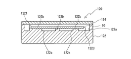
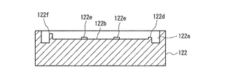
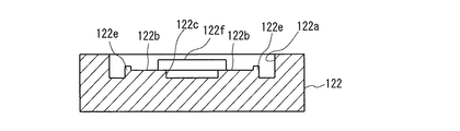
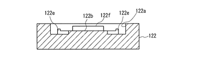
この変形例の鋳型120では、セラミックス基板10の長手方向一端部を支持する複数(図示した実施の形態では2つ)の長手方向基板支持部22dに代えて、鋳型120の幅方向(セラミックス基板10の幅方向)に延びる平面形状が略矩形の細長基板支持部122fが形成されている。この細長基板支持部122fは、セラミックス基板10の一方の面(回路パターン側の面)の周縁部と側面に当接してセラミックス基板10を所定の位置で支持するために、略L字型の断面を有するように段差が設けられている。この細長基板支持部122fは、高い側の高さが長手方向基板支持部22dより高く且つセラミックス基板10の上面より高くなっている。その他の構成は、上述した実施の形態の金属−セラミックス接合基板を製造するために使用する鋳型と略同一であるので、参照符号に100を加えてその説明を省略する。なお、ベース板12には、細長基板支持部122fに対応する(図示しない)凹部が形成されるが、この凹部は小さいため、金属−セラミックス接合基板の信頼性や熱伝導率に殆ど影響しない。
In the
[第2の実施の形態]
図6A〜図6Cは、本発明による金属−セラミックス接合基板の第2の実施の形態を示し、図7および図8A〜図8Eは、その金属−セラミックス接合基板を製造するために使用する鋳型を示している。
[Second Embodiment]
6A to 6C show a second embodiment of a metal / ceramic bonding substrate according to the present invention, and FIGS. 7 and 8A to 8E show a mold used for manufacturing the metal / ceramic bonding substrate. Show.
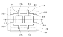
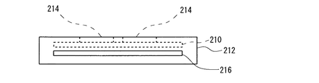
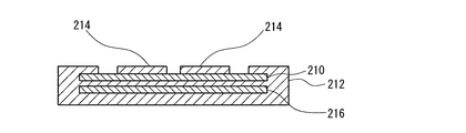
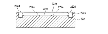
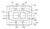
図6A〜図6Cに示すように、本発明による金属−セラミックス接合基板の第2の実施の形態では、ベース板212の内部に、平面形状が略矩形の1以上(図示した実施の形態では1つ)の板状の強化部材216がセラミックス基板210から離間して且つセラミックス基板210と略平行に配置されている。この強化部材216は、ベース板212の内部を(セラミックス基板210の幅方向に)貫通して延びており、端部が外部に露出し、ベース板212の内部を貫通して延びている部分の全面(端部以外の全面)がベース板212に直接接合している。この強化部材216は、ベース板212の材料(アルミニウムまたはアルミニウム合金)より融点が高い材料からなり、ニッケル、コバルト、銅およびマンガンからなる群から選ばれる1種以上と鉄を含有する金属、あるいはアルミナ、ジルコニア、アルミナとジルコニアの複合材、窒化アルミニウム、窒化珪素および炭化珪素からなる群から選ばれる1種以上のセラミックスなどの材料からなるのが好ましい。このような強化部材216をベース板212の内部に配置させることにより、セラミックス基板210に生じる応力を小さくすることができるとともに、金属−セラミックス接合基板の反りを小さくすることができるため、ベース板212を厚くすることができるので、ベース板212の熱容量を大きくして放熱性を向上させることができる。その他の構成は、上述した第1の実施の形態の金属−セラミックス接合基板と略同一であるので、参照符号に200を加えてその説明を省略する。
As shown in FIGS. 6A to 6C, in the second embodiment of the metal / ceramic bonding substrate according to the present invention, the
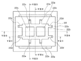
本実施の形態の金属−セラミックス接合基板は、図7に示すような鋳型220内にセラミックス基板210と強化部材216とを互いに離間して配置し、強化部材216の略全面と、セラックス基板210の両面のベース板212と回路パターン用金属板214に対応する部分に接触するように、アルミニウムまたはアルミニウム合金の溶湯を流し込んで冷却することによって製造することができる。
In the metal / ceramic bonding substrate of the present embodiment, a
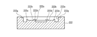
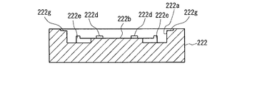
図8A〜図8Eに示すように、本実施の形態の金属−セラミックス接合基板を製造するために使用する鋳型220では、下側鋳型部材222の上面には、(ベース板212の回路パターン側の部分を形成するための凹部である)ベース板形成部222aの幅方向の両側面に、強化部材216の長手方向の両端部と略同一の形状および大きさでその両端部(の回路パターン側の部分)を収容するための1対以上(図示した実施の形態では1対)の凹部(強化部材支持部)222gが形成されている。一方、図7に示すように、上側鋳型部材224の下面には、ベース板212を形成するための凹部(ベース板形成部)224aが形成されるとともに、このベース板形成部224aの幅方向の両側面に、強化部材216の長手方向の両端部と略同一の形状および大きさでその両端部(の回路パターン側と反対側の部分)を収容するための1対以上(図示した実施の形態では1対)の凹部(強化部材支持部)が形成されている。なお、下側鋳型部材222のベース板形成部222aと上側鋳型部材224のベース形成部224aによって画定された空間内にベース板212が形成されるようになっている。また、下側鋳型部材222の強化部材支持部222gに強化部材216を収容した後に上側鋳型部材224を下側鋳型部材222に被せると、強化部材216が下側鋳型部材222の強化部材支持部222gと上側鋳型部材224の強化部材支持部によって挟持されるようになっている。このように強化部材216を挟持することにより、強化部材216を所定の位置(ベース板212の主面に沿った方向および厚さ方向の所定の位置)に精度良く固定することができる。その他の構成は、上述した第1の実施の形態の金属−セラミックス接合基板を製造するために使用する鋳型と略同一であるので、参照符号に200を加えてその説明を省略する。
As shown in FIGS. 8A to 8E, in the
[第3の実施の形態]
図9A〜図9Cは、本発明による金属−セラミックス接合基板の第3の実施の形態を示し、図10および図11A〜図11Eは、その金属−セラミックス接合基板を製造するために使用する鋳型を示している。
[Third Embodiment]
9A to 9C show a third embodiment of a metal / ceramic bonding substrate according to the present invention, and FIGS. 10 and 11A to 11E show a mold used for manufacturing the metal / ceramic bonding substrate. Show.
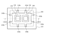
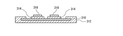
図9A〜図9Cに示すように、本発明による金属−セラミックス接合基板の第3の実施の形態では、回路パターン用金属板314の上面に電子部品318が直接接合している。その他の構成は、上述した第1の実施の形態の金属−セラミックス接合基板と略同一であるので、参照符号に300を加えてその説明を省略する。
As shown in FIGS. 9A to 9C, in the third embodiment of the metal / ceramic bonding substrate according to the present invention, the
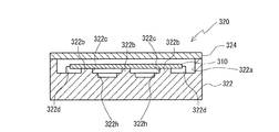
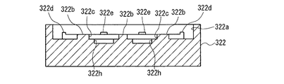
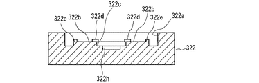
本実施の形態の金属−セラミックス接合基板は、図10に示すような鋳型320内に電子部品318とセラミックス基板310とを互いに離間して配置し、電子部品318の一方の面と、セラックス基板310の両面のベース板312と回路パターン用金属板314に対応する部分に接触するように、アルミニウムまたはアルミニウム合金の溶湯を流し込んで冷却することによって製造することができる。
In the metal / ceramic bonding substrate according to the present embodiment, an
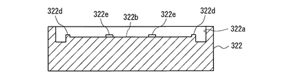
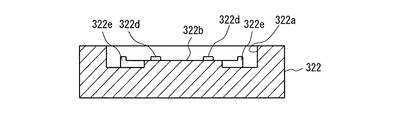
図11A〜図11Eに示すように、本実施の形態の金属−セラミックス接合基板を製造するために使用する鋳型320では、回路パターン用金属板形成部322cのそれぞれの底面に、電子部品318と略等しい形状および大きさの1つまたは複数(図示した実施の形態ではそれぞれ1つ)の凹部(電子部品収容部)322hが形成されている。その他の構成は、上述した第1の実施の形態の金属−セラミックス接合基板を製造するために使用する鋳型と略同一であるので、参照符号に300を加えてその説明を省略する。
As shown in FIGS. 11A to 11E, in the
このように、半田を使用しないで電子部品318をアルミニウムまたはアルミニウム合金からなる回路パターン用金属板314に直接接合することにより、熱伝導率を向上させて放熱性を向上させることができる。また、半田を使用した場合に生じ易いボイドが生じ難くなり、アルミニウムまたはアルミニウム合金は半田より熱伝導率が高いため、放熱性および信頼性を向上させることができる。また、鉛フリー化が難しい高温半田を使用する必要がないので、鉛フリー化を図ることができる。さらに、半田濡れ性を向上させるために回路パターン用金属板314にめっきを施す必要もない。なお、電子部品318は、金属溶湯を反応して合金または化合物を生成しない物質からなるものであれば、半導体チップ、抵抗体チップおよびコンデンサチップなどのいずれの電子部品でもよい。
Thus, by directly joining the
[第4の実施の形態]
図12A〜図12Cは、本発明による金属−セラミックス接合基板の第4の実施の形態を示し、図13は、その金属−セラミックス接合基板を製造するために使用する鋳型を示している。
[Fourth Embodiment]
12A to 12C show a fourth embodiment of a metal / ceramic bonding substrate according to the present invention, and FIG. 13 shows a mold used for manufacturing the metal / ceramic bonding substrate.
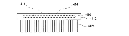
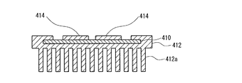
図12A〜図12Cに示すように、本発明による金属−セラミックス接合基板の第4の実施の形態では、平面形状が略矩形の複数の板状フィン412aが、互いに略平行に且つ一定の間隔で離間して、ベース板412の底面に対して略垂直方向に延びるようにその底面に一体に形成されている。その他の構成は、上述した第1の実施の形態の金属−セラミックス接合基板と略同一であるので、参照符号に400を加えてその説明を省略する。
As shown in FIGS. 12A to 12C, in the fourth embodiment of the metal / ceramic bonding substrate according to the present invention, a plurality of plate-
本実施の形態の金属−セラミックス接合基板は、図13に示すような鋳型420内にセラミックス基板410を配置し、セラックス基板410の両面のベース板412と回路パターン用金属板414に対応する部分に接触するように、アルミニウムまたはアルミニウム合金の溶湯を流し込んで冷却することによって製造することができる。
In the metal / ceramic bonding substrate according to the present embodiment, a
図13に示すように、本実施の形態の金属−セラミックス接合基板を製造するために使用する鋳型420では、上側鋳型部材424の下面に、複数の板状フィン412aを形成するための凹部(放熱フィン形成部)424aが形成されている。なお、下側鋳型部材422のベース板形成部422aと上側鋳型部材424の放熱フィン形成部424aによって画定された空間内に、ベース板412が板状フィン412aと一体に形成されるようになっている。その他の構成は、上述した第1の実施の形態の金属−セラミックス接合基板を製造するために使用する鋳型と略同一であるので、参照符号に400を加えてその説明を省略する。
As shown in FIG. 13, in the
[第5の実施の形態]
図14A〜図14Cは、本発明による金属−セラミックス接合基板の第5の実施の形態を示している。
[Fifth Embodiment]
14A to 14C show a fifth embodiment of the metal / ceramic bonding substrate according to the present invention.
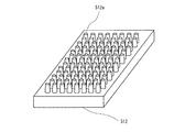
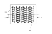
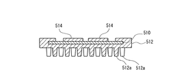
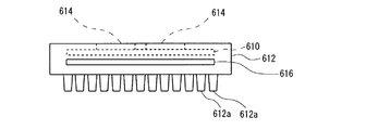
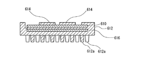
図14A〜図14Cに示すように、本発明による金属−セラミックス接合基板の第5の実施の形態では、(放熱フィンとしての)多数の柱状突起部512aが、ベース板512の底面から突出するようにベース板512と一体に形成されている。
As shown in FIGS. 14A to 14C, in the fifth embodiment of the metal / ceramic bonding substrate according to the present invention, a large number of
各々の柱状突起部512aは、略円柱形状または略円錐台形状(略円錐の上端を底面と略平行に切断した形状)を有し、ベース板512の底面に対して略垂直方向に延びている。また、柱状突起部512aは、それぞれ所定の間隔で離間して一列に配置された柱状突起部512aの複数列が互いに平行に且つ隣接する柱状突起部512aの列と互いに半ピッチ(隣接する柱状突起部512aの中心線(柱状突起部512aが延びる軸線)間の距離の半分)ずれるように配置され、隣接する柱状突起部512aの間隔を確保しながらより多くの柱状突起部512aが配置されるようにしているが、隣接する柱状突起部512aの間隔を確保しながら多数の柱状突起部512aを配置することができれば、他の配置でもよい。その他の構成は、上述した第1の実施の形態の金属−セラミックス接合基板と略同一であるので、参照符号に500を加えてその説明を省略する。
Each
本実施の形態の金属−セラミックス接合基板は、図13に示す鋳型420の複数の板状フィン412aを形成するための凹部(放熱フィン形成部)424aに代えて、多数の柱状突起部512aを形成するための凹部(柱状突起形成部)を上側鋳型部材224の下面に形成した以外は、図13に示す鋳型420と同様の鋳型内にセラミックス基板を配置し、セラックス基板の両面のベース板512と回路パターン用金属板に対応する部分に接触するように、アルミニウムまたはアルミニウム合金の溶湯を流し込んで冷却することによって製造することができる。
The metal / ceramic bonding substrate of this embodiment forms a large number of
なお、上述した第1〜第5の実施の形態を組み合わせてもよい。例えば、第1の実施の形態の変形例の細長基板支持部122fを第2〜第5の実施の形態の金属−セラミックス接合基板を製造するために使用する鋳型に適用してもよい。また、第2の実施の形態の強化部材216を第3〜第5の実施の形態の金属−セラミックス接合基板に適用してもよい。また、第3の実施の形態の電子部品収容部322hを第2、第4および第5の実施の形態の金属−セラミックス接合基板を製造するために使用する鋳型に適用してもよい。
In addition, you may combine the 1st-5th embodiment mentioned above. For example, you may apply the elongate board |
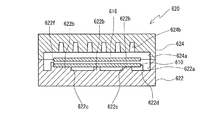
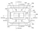
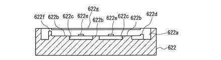
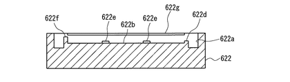
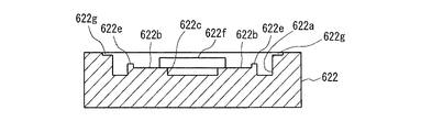
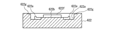
例えば、本発明による金属−セラミックス接合基板の第5の実施の形態の変形例として、図15A〜図15C、図16および図17A〜図17Eに示すように、第1の実施の形態およびその変形例と、第2の実施の形態と、第5の実施の形態とを組み合わせてもよい。この変形例の構成は、上述した第1の実施の形態およびその変形例と、第2の実施の形態と、第5の実施の形態の金属−セラミックス接合基板およびその金属−セラミックス接合基板を製造するために使用する鋳型の構成と略同一であるので、第1の実施の形態に対応する部分には参照符号に600を加え、第1の実施の形態の変形例に対応する部分には参照符号に500を加え、第2の実施の形態に対応する部分には参照符号に400を加え、第5の実施の形態に対応する部分には参照符号に100を加えてその説明を省略する。また、参照符号612cは、細長基板支持部622fに対応してベース板612に形成された凹部を示し、参照符号624bは、凹部(放熱ピン形成部)を示している。なお、細長基板支持部622fは、高い側の高さが長手方向基板支持部622dより高く且つセラミックス基板610の上面より高くなっており、鋳型620内に溶湯を注湯した際に、セラミックス基板610と強化部材616との間に残留し易いガスを外部に放出してボイド(空隙)が発生するのを防止するためのガス抜き部としても作用することができる。
For example, as a modification of the fifth embodiment of the metal / ceramic bonding substrate according to the present invention, as shown in FIGS. 15A to 15C, 16 and 17A to 17E, the first embodiment and its modifications The example, the second embodiment, and the fifth embodiment may be combined. The configuration of this modification is to produce the metal-ceramic bonding substrate and the metal-ceramic bonding substrate of the first embodiment and its modification, the second embodiment, and the fifth embodiment described above. Therefore, the reference numeral 600 is added to the part corresponding to the first embodiment, and the part corresponding to the modification of the first embodiment is referred to. 500 is added to the reference numerals, 400 is added to the reference numerals corresponding to the second embodiment, 100 is added to the reference numerals corresponding to the fifth embodiment, and the description thereof is omitted.
以下、本発明による金属−セラミックス接合基板およびその製造方法の実施例について詳細に説明する。 Hereinafter, examples of the metal / ceramic bonding substrate and the manufacturing method thereof according to the present invention will be described in detail.
[実施例1]
長さ77mm×幅56mm×厚さ0.6mmのセラミックス基板としてのAlN板を、図2に示す鋳型20と同様の鋳型内に収容した後、鋳型内を窒素雰囲気にした状態で加熱し、アルミニウム溶湯をその表面の酸化膜を取り除きながら鋳型内に注湯し、その後、鋳型を冷却して溶湯を凝固させることによって、セラミックス基板の一方の面の周縁部(の幅1.5mmの部分)と側面および他方の面の全面に(長さ79mm、幅58mm、厚さ1.7mmの)ベース板が一体に形成されるとともに、このベース板(のセラミックスの一方の面の周縁部に形成された部分)から(2mm)離間してセラミックス基板の一方の面に長さ70mm×幅49mm×厚さ0.6mmの回路パターン用アルミニウム板が形成されたベース一体型の金属−セラミックス接合基板を作製した。なお、セラミックス基板の側面に形成されたベース板の幅(セラミックス基板の側面からベース板の側面までの距離)は1mm、他方の面に形成されたベース板の厚さは0.5mm、一方の面の周縁部に形成されたベース板の厚さは0.6mmであった。
[Example 1]
After an AlN plate as a ceramic substrate having a length of 77 mm, a width of 56 mm, and a thickness of 0.6 mm is accommodated in a mold similar to the
この金属−セラミックス接合基板について、レーザー顕微鏡による3次元の高低差マップの最大値を反りとみなして、セラミックス基板の一方の面側(回路パターン用アルミニウム板側)の反りを測定したところ、セラミックス基板の他方の面側(ベース板側)が凸状に反っているときを+(プラス)として、約+130μmであった。 With regard to this metal-ceramic bonding substrate, the maximum value of the three-dimensional height difference map obtained by a laser microscope was regarded as a warp, and the warp on one surface side of the ceramic substrate (the aluminum plate side for the circuit pattern) was measured. When the other surface side (base plate side) was warped in a convex shape, it was about +130 μm, with + (plus).
[比較例1]
セラミックス基板の一方の面の周縁部にベース板を形成しないで、セラミックス基板の一方の面側のベース板と回路パターン用アルミニウム板の間隔を3.5mmとした以外は、実施例1と同様の方法により、ベース一体型の金属−セラミックス接合基板を作製し、その反りを測定したところ、約+180μmであった。
[Comparative Example 1]
The same as in Example 1 except that the base plate is not formed on the peripheral edge of one surface of the ceramic substrate, and the distance between the base plate on one surface side of the ceramic substrate and the aluminum plate for circuit pattern is 3.5 mm. A base-integrated metal / ceramic bonding substrate was prepared by the method, and the warpage thereof was measured, and it was about +180 μm.
[実施例2]
長さ71mm×幅72mm×厚さ0.6mmのセラミックス基板としてのAlN板と、長さ71mm×幅79mm×厚さ0.6mmの強化部材としてのAlN板を、図16に示す鋳型620と同様の鋳型内に収容した後、鋳型内を窒素雰囲気にした状態で加熱し、アルミニウム溶湯をその表面の酸化膜を取り除きながら鋳型内に注湯し、その後、鋳型を冷却して溶湯を凝固させることによって、セラミックス基板の一方の面の周縁部(の幅1mmの部分)と側面および他方の面の全面に(長さ98mm、幅78mm、厚さ4mmの)ベース板が一体に形成され、このベース板(のセラミックス基板の一方の面の周縁部に形成された部分)から(2mm)離間してセラミックス基板の一方の面に長さ65mm×幅66mm×厚さ0.4mmの回路パターン用アルミニウム板が形成されるとともに、ベース板の内部に強化部材がセラミックス基板から1.9mm離間して且つセラミックス基板と略平行に配置されたベース一体型の金属−セラミックス接合基板を作製した。なお、セラミックス基板の側面に形成されたベース板の幅(セラミックス基板の側面からベース板の側面までの距離)は長さ方向両端の側面では13.5mm、幅方向両端の側面では3mmであり、他方の面に形成された(内部に強化部材を含む)ベース板の厚さは3mm、一方の面の周縁部に形成されたベース板の厚さは0.4mmであった。また、ベース板の回路パターン用アルミニウム板と反対側の面に形成された柱状突起部(放熱ピン)の高さは8mm、直径は2mm、間隔は3mm、本数は525本であった。
[Example 2]
An AlN plate as a ceramic substrate having a length of 71 mm × width of 72 mm × thickness of 0.6 mm and an AlN plate as a reinforcing member having a length of 71 mm × width of 79 mm × thickness of 0.6 mm are the same as the
また、ベース板および回路パターン用アルミニウム板をセラミックス基板に直接接合させた後、回路パターン用アルミニウム板の不要部分をエッチングにより除去して(2つのアイランドからなる)回路パターンを形成した。このようにしてベース一体型の金属−セラミックス接合基板を作製し、その反りを実施例1と同様の方法により測定したところ、約+100μmであった。 Further, after the base plate and the circuit pattern aluminum plate were directly joined to the ceramic substrate, unnecessary portions of the circuit pattern aluminum plate were removed by etching to form a circuit pattern (consisting of two islands). In this way, a base-integrated metal / ceramic bonding substrate was produced, and its warpage was measured by the same method as in Example 1. As a result, it was about +100 μm.
また、このベース一体型の金属−セラミックス接合基板のベース板の4つの角部の各々において長さ方向および幅方向のそれぞれの端部から6mm離間した位置を中心とする直径6mmのねじ穴を機械加工によりベース板を厚さ方向に延びるように形成し、柱状突起部(放熱ピン)を覆うように水冷ジャケットをねじ止めし、金属−セラミックス接合基板と水冷ジャケットによって画定された空間に水を流したところ、水漏れの問題はなかった。 In addition, a screw hole having a diameter of 6 mm is formed at each of the four corners of the base plate of the base-integrated metal / ceramic bonding substrate at a position 6 mm away from each end in the length direction and the width direction. The base plate is formed to extend in the thickness direction by processing, and the water cooling jacket is screwed to cover the columnar protrusions (radiation pins), and water flows into the space defined by the metal / ceramic bonding substrate and the water cooling jacket. As a result, there was no problem of water leakage.
[比較例2]
セラミックス基板の一方の面の周縁部にベース板を形成しないで、セラミックス基板の一方の面側のベース板と回路パターン用アルミニウム板の間隔を3mmとした以外は、実施例2と同様の方法により、ベース一体型の金属−セラミックス接合基板を作製し、その反りを測定したところ、±100μmであり、反りの方向が安定しなかった。また、実施例2と同様の方法により、水冷ジャケットをねじ止めして水を流したところ、水漏れが発生した。
[Comparative Example 2]
According to the same method as in Example 2, except that the base plate is not formed on the peripheral portion of one surface of the ceramic substrate and the distance between the base plate on one surface side of the ceramic substrate and the aluminum plate for circuit pattern is 3 mm. When a base-integrated metal-ceramic bonding substrate was prepared and its warpage was measured, it was ± 100 μm and the direction of warpage was not stable. Moreover, when the water cooling jacket was screwed and water was flowed by the same method as in Example 2, water leakage occurred.
[実施例3]
長さ70mm×幅71mm×厚さ0.6mmのセラミックス基板としてのAlN板と、長さ70mm×幅84mm×厚さ0.6mmの強化部材としてのAlN板を、図16に示す鋳型620と同様の鋳型内に収容した後、鋳型内を窒素雰囲気にした状態で加熱し、アルミニウム溶湯をその表面の酸化膜を取り除きながら鋳型内に注湯し、その後、鋳型を冷却して溶湯を凝固させることによって、セラミックス基板の一方の面の周縁(の幅0.4mmの部分)部と側面および他方の面の全面に(長さ98mm、幅81mm、厚さ3.9mmの)ベース板が一体に形成され、このベース板(のセラミックス基板の一方の面の周縁部に形成された部分)から(2mm)離間してセラミックス基板の一方の面に長さ65mm×幅66mm×厚さ0.6mmの回路パターン用アルミニウム板が形成されるとともに、ベース板の内部に強化部材がセラミックス基板から1.5mm離間して且つセラミックス基板と略平行に配置されたベース一体型の金属−セラミックス接合基板を作製した。なお、セラミックス基板の側面に形成されたベース板の幅(セラミックス基板の側面からベース板の側面までの距離)は長さ方向両端の側面では14mm、幅方向両端の側面では5mmであり、他方の面に形成された(内部に強化部材を含む)ベース板の厚さは2.7mm、一方の面の周縁部に形成されたベース板の厚さは0.6mmであった。また、ベース板の回路パターン用アルミニウム板と反対側の面に形成された柱状突起部(放熱ピン)の高さは8mm、直径は2mm、間隔は3mm、本数は525本であった。
[Example 3]
An AlN plate as a ceramic substrate having a length of 70 mm × width 71 mm × thickness 0.6 mm and an AlN plate as a reinforcing member having a length 70 mm × width 84 mm × thickness 0.6 mm are similar to the
このようにして作製した30個のベース一体型の金属−セラミックス接合基板の各々の反りを実施例1と同様の方法により測定したところ、平均約+150μmであった。また、作製したベース一体型の金属−セラミックス接合基板の断面をX線検査装置で観察したところ、ボイドは確認されなかった。 The warpage of each of the 30 base-integrated metal / ceramic bonding substrates prepared in this manner was measured by the same method as in Example 1, and the average was about +150 μm. Further, when a cross section of the produced base-integrated metal / ceramic bonding substrate was observed with an X-ray inspection apparatus, no voids were confirmed.
また、このベース一体型の金属−セラミックス接合基板のベース板の4つの角部の各々において長さ方向および幅方向のそれぞれの端部から6mm離間した位置を中心とする直径6mmのねじ穴を機械加工によりベース板を厚さ方向に延びるように形成し、柱状突起部(放熱ピン)を覆うように水冷ジャケットをねじ止めし、金属−セラミックス接合基板と水冷ジャケットによって画定された空間に水を流したところ、水漏れの問題はなかった。 In addition, a screw hole having a diameter of 6 mm is formed at each of the four corners of the base plate of the base-integrated metal / ceramic bonding substrate at a position 6 mm away from each end in the length direction and the width direction. The base plate is formed to extend in the thickness direction by processing, and the water cooling jacket is screwed to cover the columnar protrusions (radiation pins), and water flows into the space defined by the metal / ceramic bonding substrate and the water cooling jacket. As a result, there was no problem of water leakage.
なお、細長基板支持部622fの高い側の高さを長手方向基板支持部622dと同じ高さでセラミックス基板610の上面より低くした以外は、図16に示す鋳型620と同様の鋳型を使用して、実施例3と同様の方法により、30個のベース一体型の金属−セラミックス接合基板を作製して、反りとボイドの発生を確認したところ、反りは平均約+150μmであったが、いずれもセラミックス基板と強化部材の間にボイドが確認された。
A mold similar to the
[実施例4]
長さ70mm×幅71mm×厚さ0.6mmのセラミックス基板としてのAlN板と、長さ70mm×幅84mm×厚さ0.6mmの強化部材としてのAlN板を、図7に示す鋳型220と同様の鋳型内に収容した後、鋳型内を窒素雰囲気にした状態で加熱し、アルミニウム溶湯をその表面の酸化膜を取り除きながら鋳型内に注湯し、その後、鋳型を冷却して溶湯を凝固させることによって、セラミックス基板の一方の面の周縁部(の幅0.4mmの部分)と側面および他方の面の全面に(長さ98mm、幅81mm、厚さ3.9mmの)ベース板が一体に形成され、このベース板(のセラミックス基板の一方の面の周縁部に形成された部分)から(2mm)離間してセラミックス基板の一方の面に長さ65mm×幅66mm×厚さ0.6mmの回路パターン用アルミニウム板が形成されるとともに、ベース板の内部に強化部材がセラミックス基板から1.5mm離間して且つセラミックス基板と略平行に配置されたベース一体型の金属−セラミックス接合基板を作製した。なお、セラミックス基板の側面に形成されたベース板の幅(セラミックス基板の側面からベース板の側面までの距離)は長さ方向両端の側面では14mm、幅方向両端の側面では5mmであり、他方の面に形成された(内部に強化部材を含む)ベース板の厚さは2.7mm、一方の面の周縁部に形成されたベース板の厚さは0.6mmであった。
[Example 4]
An AlN plate as a ceramic substrate having a length of 70 mm × width of 71 mm × thickness of 0.6 mm and an AlN plate as a reinforcing member having a length of 70 mm × width of 84 mm × thickness of 0.6 mm are the same as the
このようにして作製したベース一体型の金属−セラミックス接合基板の反りを実施例1と同様の方法により測定したところ、約+150μmであった。 The warpage of the base-integrated metal / ceramic bonding substrate thus prepared was measured by the same method as in Example 1, and was about +150 μm.
また、このベース一体型の金属−セラミックス接合基板のベース板の4つの角部の各々において長さ方向および幅方向のそれぞれの端部から6mm離間した位置を中心とする直径6mmのねじ穴を機械加工によりベース板を厚さ方向に延びるように形成し、柱状突起部(放熱ピン)を覆うように水冷ジャケットをねじ止めし、金属−セラミックス接合基板と水冷ジャケットによって画定された空間に水を流したところ、水漏れの問題はなかった。 In addition, a screw hole having a diameter of 6 mm is formed at each of the four corners of the base plate of the base-integrated metal / ceramic bonding substrate at a position 6 mm away from each end in the length direction and the width direction. The base plate is formed to extend in the thickness direction by processing, and the water cooling jacket is screwed to cover the columnar protrusions (radiation pins), and water flows into the space defined by the metal / ceramic bonding substrate and the water cooling jacket. As a result, there was no problem of water leakage.
10、210、310、410、510、610 セラミックス基板
12、212、312、412、512、612 ベース板
12b、212b、312b、412b、612b、612b 凹部
14、214、314、414、514、614 回路パターン用金属板
20、120、220、320、420、620 鋳型
22、122、222、322、422、622 下側鋳型部材
22a、122a、222a、322a、422a、622a ベース板形成部
22b、122b、222b、322b、422b、622b 隆起部
22c、122c、222c、322c、422c、622c 凹部(回路パターン用金属板形成部)
22d、122d、222d、322d、422d、622d 長手方向基板支持部
22e、122e、222e、322e、622e、622e 幅方向基板支持部
24、124、224、324、424、624 上側鋳型部材
122f、622f 細長基板支持部
222g、622g 凹部(強化部材支持部)
224a、624a 凹部(ベース板形成部)
216、616 強化部材
318 電子部品
322h 凹部(電子部品収容部)
412a 板状フィン
424a 凹部(放熱フィン形成部)
512a、612a 柱状突起部
612c 凹部
624b 凹部(放熱ピン形成部)
10, 210, 310, 410, 510, 610
22d, 122d, 222d, 322d, 422d, 622d
224a, 624a Recessed portion (base plate forming portion)
216, 616 Reinforcing
412a Plate-
512a, 612a Columnar protrusion
Claims (15)
Priority Applications (1)
| Application Number | Priority Date | Filing Date | Title |
|---|---|---|---|
| JP2016121344A JP6799392B2 (en) | 2016-06-20 | 2016-06-20 | Metal-ceramic bonded substrate and its manufacturing method |
Applications Claiming Priority (1)
| Application Number | Priority Date | Filing Date | Title |
|---|---|---|---|
| JP2016121344A JP6799392B2 (en) | 2016-06-20 | 2016-06-20 | Metal-ceramic bonded substrate and its manufacturing method |
Publications (2)
| Publication Number | Publication Date |
|---|---|
| JP2017228551A true JP2017228551A (en) | 2017-12-28 |
| JP6799392B2 JP6799392B2 (en) | 2020-12-16 |
Family
ID=60889350
Family Applications (1)
| Application Number | Title | Priority Date | Filing Date |
|---|---|---|---|
| JP2016121344A Active JP6799392B2 (en) | 2016-06-20 | 2016-06-20 | Metal-ceramic bonded substrate and its manufacturing method |
Country Status (1)
| Country | Link |
|---|---|
| JP (1) | JP6799392B2 (en) |
Cited By (3)
| Publication number | Priority date | Publication date | Assignee | Title |
|---|---|---|---|---|
| JP2020050548A (en) * | 2018-09-27 | 2020-04-02 | Dowaメタルテック株式会社 | Metal-ceramic bonding substrate and method of manufacturing the same |
| CN112563224A (en) * | 2020-12-04 | 2021-03-26 | 合肥圣达电子科技实业有限公司 | Micro-channel device for heat dissipation of high-power semiconductor chip |
| WO2022209024A1 (en) * | 2021-03-31 | 2022-10-06 | Dowaメタルテック株式会社 | Metal-ceramic bonded substrate and manufacturing method therefor |
Citations (6)
| Publication number | Priority date | Publication date | Assignee | Title |
|---|---|---|---|---|
| JP2003229531A (en) * | 2002-02-05 | 2003-08-15 | Sanyo Electric Co Ltd | Hybrid integrated circuit device and method of manufacturing the same |
| JP2005072062A (en) * | 2003-08-27 | 2005-03-17 | Dowa Mining Co Ltd | Electronic component mounting substrate and manufacturing method thereof |
| JP2006156994A (en) * | 2004-11-05 | 2006-06-15 | Dowa Mining Co Ltd | Electronic component mounting substrate, manufacturing apparatus and manufacturing method thereof |
| WO2008123172A1 (en) * | 2007-03-27 | 2008-10-16 | Ngk Insulators, Ltd. | Heat spreader module, heat sink and method for manufacturing the heat spreader module and the heat sink |
| JP2009026957A (en) * | 2007-07-19 | 2009-02-05 | Ngk Insulators Ltd | Insulating fins and heat sink |
| JP2014082466A (en) * | 2012-09-27 | 2014-05-08 | Dowa Metaltech Kk | Heat sink and manufacturing method thereof |
-
2016
- 2016-06-20 JP JP2016121344A patent/JP6799392B2/en active Active
Patent Citations (6)
| Publication number | Priority date | Publication date | Assignee | Title |
|---|---|---|---|---|
| JP2003229531A (en) * | 2002-02-05 | 2003-08-15 | Sanyo Electric Co Ltd | Hybrid integrated circuit device and method of manufacturing the same |
| JP2005072062A (en) * | 2003-08-27 | 2005-03-17 | Dowa Mining Co Ltd | Electronic component mounting substrate and manufacturing method thereof |
| JP2006156994A (en) * | 2004-11-05 | 2006-06-15 | Dowa Mining Co Ltd | Electronic component mounting substrate, manufacturing apparatus and manufacturing method thereof |
| WO2008123172A1 (en) * | 2007-03-27 | 2008-10-16 | Ngk Insulators, Ltd. | Heat spreader module, heat sink and method for manufacturing the heat spreader module and the heat sink |
| JP2009026957A (en) * | 2007-07-19 | 2009-02-05 | Ngk Insulators Ltd | Insulating fins and heat sink |
| JP2014082466A (en) * | 2012-09-27 | 2014-05-08 | Dowa Metaltech Kk | Heat sink and manufacturing method thereof |
Cited By (6)
| Publication number | Priority date | Publication date | Assignee | Title |
|---|---|---|---|---|
| JP2020050548A (en) * | 2018-09-27 | 2020-04-02 | Dowaメタルテック株式会社 | Metal-ceramic bonding substrate and method of manufacturing the same |
| JP7157609B2 (en) | 2018-09-27 | 2022-10-20 | Dowaメタルテック株式会社 | METAL-CERAMIC BONDING SUBSTRATE AND MANUFACTURING METHOD THEREOF |
| CN112563224A (en) * | 2020-12-04 | 2021-03-26 | 合肥圣达电子科技实业有限公司 | Micro-channel device for heat dissipation of high-power semiconductor chip |
| WO2022209024A1 (en) * | 2021-03-31 | 2022-10-06 | Dowaメタルテック株式会社 | Metal-ceramic bonded substrate and manufacturing method therefor |
| JP2022157171A (en) * | 2021-03-31 | 2022-10-14 | Dowaメタルテック株式会社 | Metal-ceramic bonded substrate and manufacturing method thereof |
| JP7649183B2 (en) | 2021-03-31 | 2025-03-19 | Dowaメタルテック株式会社 | Metal-ceramic bonded substrate and manufacturing method thereof |
Also Published As
| Publication number | Publication date |
|---|---|
| JP6799392B2 (en) | 2020-12-16 |
Similar Documents
| Publication | Publication Date | Title |
|---|---|---|
| JP6224960B2 (en) | Heat sink and manufacturing method thereof | |
| JP5837754B2 (en) | Metal-ceramic bonding substrate and manufacturing method thereof | |
| JPH0325022B2 (en) | ||
| JP5619437B2 (en) | Method for producing metal / ceramic bonding substrate | |
| JP5136748B2 (en) | Element positioning jig and mounting method | |
| JP2008218938A (en) | Metal-ceramics bonded substrate | |
| JP6799392B2 (en) | Metal-ceramic bonded substrate and its manufacturing method | |
| WO2018131583A1 (en) | Metal-ceramic bonded substrate and manufacturing method therefor | |
| JP4496404B2 (en) | Metal-ceramic bonding substrate and manufacturing method thereof | |
| JP4806803B2 (en) | Metal-ceramic bonding substrate and manufacturing method thereof | |
| US20200149829A1 (en) | Heatsink | |
| JP5389595B2 (en) | Metal-ceramic bonding substrate and manufacturing method thereof | |
| JP4565249B2 (en) | Metal-ceramic bonding substrate and manufacturing method thereof | |
| US11983586B2 (en) | Ceramic circuit board, heat-dissipating member, and aluminum-diamond composite | |
| JP5631446B2 (en) | Method for producing metal / ceramic bonding substrate | |
| JP7157609B2 (en) | METAL-CERAMIC BONDING SUBSTRATE AND MANUFACTURING METHOD THEREOF | |
| JP7769511B2 (en) | Metal-ceramic bonded substrate and manufacturing method thereof | |
| JP7267030B2 (en) | METAL-CERAMIC BONDING SUBSTRATE AND MANUFACTURING METHOD THEREOF | |
| JP5380734B2 (en) | Aluminum joint member | |
| JP7796512B2 (en) | Metal-ceramic bonded substrate and manufacturing method thereof | |
| JP7769514B2 (en) | Metal-ceramic bonded substrate and manufacturing method thereof | |
| JP3901109B2 (en) | Manufacturing method of heat radiator, heat radiator, power module substrate and power module using the heat radiator | |
| JPH10270614A (en) | Heat sink and semiconductor device | |
| JP2022157227A (en) | Metal-ceramic bonded substrate and manufacturing method thereof | |
| JP2004356303A (en) | Power module substrate, radiator, and method of manufacturing radiator |
Legal Events
| Date | Code | Title | Description |
|---|---|---|---|
| A621 | Written request for application examination |
Free format text: JAPANESE INTERMEDIATE CODE: A621 Effective date: 20190531 |
|
| A977 | Report on retrieval |
Free format text: JAPANESE INTERMEDIATE CODE: A971007 Effective date: 20200306 |
|
| A131 | Notification of reasons for refusal |
Free format text: JAPANESE INTERMEDIATE CODE: A131 Effective date: 20200323 |
|
| A521 | Request for written amendment filed |
Free format text: JAPANESE INTERMEDIATE CODE: A523 Effective date: 20200513 |
|
| A131 | Notification of reasons for refusal |
Free format text: JAPANESE INTERMEDIATE CODE: A131 Effective date: 20201027 |
|
| A521 | Request for written amendment filed |
Free format text: JAPANESE INTERMEDIATE CODE: A523 Effective date: 20201104 |
|
| TRDD | Decision of grant or rejection written | ||
| A01 | Written decision to grant a patent or to grant a registration (utility model) |
Free format text: JAPANESE INTERMEDIATE CODE: A01 Effective date: 20201117 |
|
| A61 | First payment of annual fees (during grant procedure) |
Free format text: JAPANESE INTERMEDIATE CODE: A61 Effective date: 20201120 |
|
| R150 | Certificate of patent or registration of utility model |
Ref document number: 6799392 Country of ref document: JP Free format text: JAPANESE INTERMEDIATE CODE: R150 |
|
| R250 | Receipt of annual fees |
Free format text: JAPANESE INTERMEDIATE CODE: R250 |
|
| R250 | Receipt of annual fees |
Free format text: JAPANESE INTERMEDIATE CODE: R250 |
|
| R250 | Receipt of annual fees |
Free format text: JAPANESE INTERMEDIATE CODE: R250 |