JP4770710B2 - 記録媒体およびその製造方法、並びに記録媒体用原盤およびその製造方法 - Google Patents
記録媒体およびその製造方法、並びに記録媒体用原盤およびその製造方法 Download PDFInfo
- Publication number
- JP4770710B2 JP4770710B2 JP2006308483A JP2006308483A JP4770710B2 JP 4770710 B2 JP4770710 B2 JP 4770710B2 JP 2006308483 A JP2006308483 A JP 2006308483A JP 2006308483 A JP2006308483 A JP 2006308483A JP 4770710 B2 JP4770710 B2 JP 4770710B2
- Authority
- JP
- Japan
- Prior art keywords
- groove
- layer
- recording medium
- information
- area
- Prior art date
- Legal status (The legal status is an assumption and is not a legal conclusion. Google has not performed a legal analysis and makes no representation as to the accuracy of the status listed.)
- Expired - Fee Related
Links
Images


Classifications
-
- G—PHYSICS
- G11—INFORMATION STORAGE
- G11B—INFORMATION STORAGE BASED ON RELATIVE MOVEMENT BETWEEN RECORD CARRIER AND TRANSDUCER
- G11B7/00—Recording or reproducing by optical means, e.g. recording using a thermal beam of optical radiation by modifying optical properties or the physical structure, reproducing using an optical beam at lower power by sensing optical properties; Record carriers therefor
- G11B7/24—Record carriers characterised by shape, structure or physical properties, or by the selection of the material
- G11B7/241—Record carriers characterised by shape, structure or physical properties, or by the selection of the material characterised by the selection of the material
- G11B7/242—Record carriers characterised by shape, structure or physical properties, or by the selection of the material characterised by the selection of the material of recording layers
- G11B7/243—Record carriers characterised by shape, structure or physical properties, or by the selection of the material characterised by the selection of the material of recording layers comprising inorganic materials only, e.g. ablative layers
-
- G—PHYSICS
- G11—INFORMATION STORAGE
- G11B—INFORMATION STORAGE BASED ON RELATIVE MOVEMENT BETWEEN RECORD CARRIER AND TRANSDUCER
- G11B7/00—Recording or reproducing by optical means, e.g. recording using a thermal beam of optical radiation by modifying optical properties or the physical structure, reproducing using an optical beam at lower power by sensing optical properties; Record carriers therefor
- G11B7/24—Record carriers characterised by shape, structure or physical properties, or by the selection of the material
- G11B7/2407—Tracks or pits; Shape, structure or physical properties thereof
- G11B7/24073—Tracks
-
- G—PHYSICS
- G11—INFORMATION STORAGE
- G11B—INFORMATION STORAGE BASED ON RELATIVE MOVEMENT BETWEEN RECORD CARRIER AND TRANSDUCER
- G11B7/00—Recording or reproducing by optical means, e.g. recording using a thermal beam of optical radiation by modifying optical properties or the physical structure, reproducing using an optical beam at lower power by sensing optical properties; Record carriers therefor
- G11B7/007—Arrangement of the information on the record carrier, e.g. form of tracks, actual track shape, e.g. wobbled, or cross-section, e.g. v-shaped; Sequential information structures, e.g. sectoring or header formats within a track
- G11B7/00736—Auxiliary data, e.g. lead-in, lead-out, Power Calibration Area [PCA], Burst Cutting Area [BCA], control information
-
- G—PHYSICS
- G11—INFORMATION STORAGE
- G11B—INFORMATION STORAGE BASED ON RELATIVE MOVEMENT BETWEEN RECORD CARRIER AND TRANSDUCER
- G11B7/00—Recording or reproducing by optical means, e.g. recording using a thermal beam of optical radiation by modifying optical properties or the physical structure, reproducing using an optical beam at lower power by sensing optical properties; Record carriers therefor
- G11B7/24—Record carriers characterised by shape, structure or physical properties, or by the selection of the material
- G11B7/2403—Layers; Shape, structure or physical properties thereof
- G11B7/24035—Recording layers
- G11B7/24038—Multiple laminated recording layers
-
- G—PHYSICS
- G11—INFORMATION STORAGE
- G11B—INFORMATION STORAGE BASED ON RELATIVE MOVEMENT BETWEEN RECORD CARRIER AND TRANSDUCER
- G11B7/00—Recording or reproducing by optical means, e.g. recording using a thermal beam of optical radiation by modifying optical properties or the physical structure, reproducing using an optical beam at lower power by sensing optical properties; Record carriers therefor
- G11B7/24—Record carriers characterised by shape, structure or physical properties, or by the selection of the material
- G11B7/2407—Tracks or pits; Shape, structure or physical properties thereof
- G11B7/24073—Tracks
- G11B7/24079—Width or depth
-
- G—PHYSICS
- G11—INFORMATION STORAGE
- G11B—INFORMATION STORAGE BASED ON RELATIVE MOVEMENT BETWEEN RECORD CARRIER AND TRANSDUCER
- G11B7/00—Recording or reproducing by optical means, e.g. recording using a thermal beam of optical radiation by modifying optical properties or the physical structure, reproducing using an optical beam at lower power by sensing optical properties; Record carriers therefor
- G11B7/24—Record carriers characterised by shape, structure or physical properties, or by the selection of the material
- G11B7/26—Apparatus or processes specially adapted for the manufacture of record carriers
- G11B7/261—Preparing a master, e.g. exposing photoresist, electroforming
-
- G—PHYSICS
- G11—INFORMATION STORAGE
- G11B—INFORMATION STORAGE BASED ON RELATIVE MOVEMENT BETWEEN RECORD CARRIER AND TRANSDUCER
- G11B7/00—Recording or reproducing by optical means, e.g. recording using a thermal beam of optical radiation by modifying optical properties or the physical structure, reproducing using an optical beam at lower power by sensing optical properties; Record carriers therefor
- G11B7/24—Record carriers characterised by shape, structure or physical properties, or by the selection of the material
- G11B7/241—Record carriers characterised by shape, structure or physical properties, or by the selection of the material characterised by the selection of the material
- G11B7/242—Record carriers characterised by shape, structure or physical properties, or by the selection of the material characterised by the selection of the material of recording layers
- G11B7/243—Record carriers characterised by shape, structure or physical properties, or by the selection of the material characterised by the selection of the material of recording layers comprising inorganic materials only, e.g. ablative layers
- G11B2007/24302—Metals or metalloids
- G11B2007/24312—Metals or metalloids group 14 elements (e.g. Si, Ge, Sn)
-
- G—PHYSICS
- G11—INFORMATION STORAGE
- G11B—INFORMATION STORAGE BASED ON RELATIVE MOVEMENT BETWEEN RECORD CARRIER AND TRANSDUCER
- G11B7/00—Recording or reproducing by optical means, e.g. recording using a thermal beam of optical radiation by modifying optical properties or the physical structure, reproducing using an optical beam at lower power by sensing optical properties; Record carriers therefor
- G11B7/24—Record carriers characterised by shape, structure or physical properties, or by the selection of the material
- G11B7/241—Record carriers characterised by shape, structure or physical properties, or by the selection of the material characterised by the selection of the material
- G11B7/242—Record carriers characterised by shape, structure or physical properties, or by the selection of the material characterised by the selection of the material of recording layers
- G11B7/243—Record carriers characterised by shape, structure or physical properties, or by the selection of the material characterised by the selection of the material of recording layers comprising inorganic materials only, e.g. ablative layers
- G11B2007/24302—Metals or metalloids
- G11B2007/24314—Metals or metalloids group 15 elements (e.g. Sb, Bi)
-
- G—PHYSICS
- G11—INFORMATION STORAGE
- G11B—INFORMATION STORAGE BASED ON RELATIVE MOVEMENT BETWEEN RECORD CARRIER AND TRANSDUCER
- G11B7/00—Recording or reproducing by optical means, e.g. recording using a thermal beam of optical radiation by modifying optical properties or the physical structure, reproducing using an optical beam at lower power by sensing optical properties; Record carriers therefor
- G11B7/24—Record carriers characterised by shape, structure or physical properties, or by the selection of the material
- G11B7/241—Record carriers characterised by shape, structure or physical properties, or by the selection of the material characterised by the selection of the material
- G11B7/242—Record carriers characterised by shape, structure or physical properties, or by the selection of the material characterised by the selection of the material of recording layers
- G11B7/243—Record carriers characterised by shape, structure or physical properties, or by the selection of the material characterised by the selection of the material of recording layers comprising inorganic materials only, e.g. ablative layers
- G11B2007/24302—Metals or metalloids
- G11B2007/24316—Metals or metalloids group 16 elements (i.e. chalcogenides, Se, Te)
-
- G—PHYSICS
- G11—INFORMATION STORAGE
- G11B—INFORMATION STORAGE BASED ON RELATIVE MOVEMENT BETWEEN RECORD CARRIER AND TRANSDUCER
- G11B7/00—Recording or reproducing by optical means, e.g. recording using a thermal beam of optical radiation by modifying optical properties or the physical structure, reproducing using an optical beam at lower power by sensing optical properties; Record carriers therefor
- G11B7/24—Record carriers characterised by shape, structure or physical properties, or by the selection of the material
- G11B7/241—Record carriers characterised by shape, structure or physical properties, or by the selection of the material characterised by the selection of the material
- G11B7/252—Record carriers characterised by shape, structure or physical properties, or by the selection of the material characterised by the selection of the material of layers other than recording layers
- G11B7/253—Record carriers characterised by shape, structure or physical properties, or by the selection of the material characterised by the selection of the material of layers other than recording layers of substrates
- G11B7/2533—Record carriers characterised by shape, structure or physical properties, or by the selection of the material characterised by the selection of the material of layers other than recording layers of substrates comprising resins
- G11B7/2534—Record carriers characterised by shape, structure or physical properties, or by the selection of the material characterised by the selection of the material of layers other than recording layers of substrates comprising resins polycarbonates [PC]
-
- G—PHYSICS
- G11—INFORMATION STORAGE
- G11B—INFORMATION STORAGE BASED ON RELATIVE MOVEMENT BETWEEN RECORD CARRIER AND TRANSDUCER
- G11B7/00—Recording or reproducing by optical means, e.g. recording using a thermal beam of optical radiation by modifying optical properties or the physical structure, reproducing using an optical beam at lower power by sensing optical properties; Record carriers therefor
- G11B7/24—Record carriers characterised by shape, structure or physical properties, or by the selection of the material
- G11B7/241—Record carriers characterised by shape, structure or physical properties, or by the selection of the material characterised by the selection of the material
- G11B7/252—Record carriers characterised by shape, structure or physical properties, or by the selection of the material characterised by the selection of the material of layers other than recording layers
- G11B7/257—Record carriers characterised by shape, structure or physical properties, or by the selection of the material characterised by the selection of the material of layers other than recording layers of layers having properties involved in recording or reproduction, e.g. optical interference layers or sensitising layers or dielectric layers, which are protecting the recording layers
-
- G—PHYSICS
- G11—INFORMATION STORAGE
- G11B—INFORMATION STORAGE BASED ON RELATIVE MOVEMENT BETWEEN RECORD CARRIER AND TRANSDUCER
- G11B7/00—Recording or reproducing by optical means, e.g. recording using a thermal beam of optical radiation by modifying optical properties or the physical structure, reproducing using an optical beam at lower power by sensing optical properties; Record carriers therefor
- G11B7/24—Record carriers characterised by shape, structure or physical properties, or by the selection of the material
- G11B7/241—Record carriers characterised by shape, structure or physical properties, or by the selection of the material characterised by the selection of the material
- G11B7/252—Record carriers characterised by shape, structure or physical properties, or by the selection of the material characterised by the selection of the material of layers other than recording layers
- G11B7/258—Record carriers characterised by shape, structure or physical properties, or by the selection of the material characterised by the selection of the material of layers other than recording layers of reflective layers
- G11B7/259—Record carriers characterised by shape, structure or physical properties, or by the selection of the material characterised by the selection of the material of layers other than recording layers of reflective layers based on silver
Landscapes
- Chemical & Material Sciences (AREA)
- Inorganic Chemistry (AREA)
- Engineering & Computer Science (AREA)
- Manufacturing & Machinery (AREA)
- Optical Recording Or Reproduction (AREA)
- Optical Record Carriers And Manufacture Thereof (AREA)
- Manufacturing Optical Record Carriers (AREA)
Description
第1の領域に第1のグルーブが形成され、第2の領域に第2のグルーブが形成された基板と、
基板上に形成された少なくとも2層以上の情報層と、
情報層上に形成された透明保護層と
を備え、
第1の領域は、媒体に固有の情報が記録される固有情報記録領域であり、
第2の領域は、データ記録領域であり、
第1の領域には、固有の情報が予め所定の2値情報として記録されており、
2値情報は、複数の第1のグルーブを横断して半径方向に延びるマークにより記録されており、
第1のグルーブの深さが第2のグルーブの深さに比して浅く、または第1のグルーブの幅が第2のグルーブの幅に比して狭くされた記録媒体である。
樹脂材料に対してスタンパの転写面の形状を転写して基板を成形する工程と、
基板上に少なくとも2層以上の情報層を形成する工程と、
情報層上に透明保護層を形成する工程と
を備え、
スタンパは、
基板の第1の領域に対して第1のグルーブを形成する第1のスタンパグルーブと、
基板の第2の領域に対して第2のグルーブを形成する第2のスタンパグルーブと
を備え、
第1の領域は、媒体に固有の情報が記録される固有情報記録領域であり、
第2の領域は、データ記録領域であり、
第1の領域には、固有の情報が予め所定の2値情報として記録されており、
2値情報は、複数の第1のグルーブを横断して半径方向に延びるマークにより記録されており、
第1のスタンパグルーブの深さが、第2のスタンパグルーブの深さに比して浅く、または第1のスタンパグルーブの幅が、第2のスタンパグルーブの幅に比して狭くされた記録媒体の製造方法である。
以下、この発明の理解を容易とするために、この発明の概要について2層のBDを例として説明する。
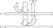
まず、図1を参照して、L0層2およびL1層4の反射率の関係について説明する。
L0層2およびL1層4からの反射光量が等しいと仮定すると、以下の関係式が成立する。
R1=T1・R0・T1 ・・・(1)
但し、R0:L0層2の反射率、R1:L1層4の反射率、T1:L1層4の透過率
1−R1−T1=T1−T1・R0 ・・・(2)
R0=((R1+1)2±√((R1+1)4−16R1 2))/2R1 ・・・(3)
となる。
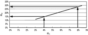
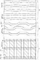
ここで、0≦R0≦1であることより複合の「−」のみが解となる。そこで、式(3)の反射率R1と反射率R0の関係をグラフで表すと、図2のようになる。
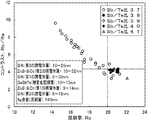
反射率とコントラストは多重干渉の計算により図3のような関係になる。これは、反射率を上げようとするとコントラストが減少するということを表している。
サンプルは、基板上に、Ag合金層(反射層)、SiN層(第2の誘電体層)、ZnS−SiO2層(第1の誘電体層)、SbTe系相変化記録層(相変化記録層)、SiN層(第1の誘電体層)、ZnS−SiO2層(第2の誘電体層)、SiN層(第3の誘電体層)を順次積層した構成を有する。各サンプルの膜厚およびSb/Te比は、表1に示すように変化させた。

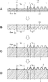
以下、この発明の一実施形態について図面を参照しながら説明する。図5は、この発明の一実施形態による光ディスクの構成の一例を示す。図6は、この発明の一実施形態による光ディスクのより具体的な構成の一例を示す。図7は、この発明の一実施形態による光ディスクの具体的な膜構成の一例を示す。
以下、光ディスクを構成する基板1、L0層2、L1層4、中間層3、カバー層5について順次説明する。
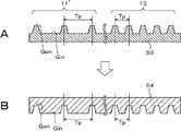
基板1は、中央に開口(以下、センターホールと称する)が形成された円環形状を有する。この基板1の一主面は、凹凸面となっており、この凹凸面上にL0層2が成膜される。以下では、凹凸面のうちレーザ光入射面Sから遠い凹部をイングルーブGin、凹凸面のうちレーザ光入射面Sから近い凸部をオングルーブGonと称する。なお、基板1のBCA11に設けられた凸状のオングルーブGonが、第1のグルーブの一例であり、基板1のデータ記録領域13に設けられた凸状のオングルーブGonが、第2のグルーブの一例である。
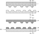
情報記録層であるL0層2およびL1層4は、基板1の凹凸上に成膜された記録膜などから構成される層をいう。L0層2は、反射層6a、第2の誘電体層52a、第1の誘電体層51a、相変化記録層8a、第1の誘電体層53a、第2の誘電体層54a、第3の誘電体層55aを基板1上に順次積層してなる積層膜である。
第2の誘電体層52a、第1の誘電体層53a、第3の誘電体層55aを構成する材料としては、例えばSiNを用いることができる。第1の誘電体層51aおよび第2の誘電体層54aを構成する材料としては、例えばZnS−SiO2を用いることができる。
基板1に形成されたL0層2上には、例えば、厚さ25μmを有する樹脂層としての中間層3が形成される。この中間層3は、透明性を有する樹脂材料からなり、このような材料としては、例えばポリカーボネート系樹脂、ポリオレフィン系樹脂若しくはアクリル系樹脂などのプラスチック材料を用いることができる。中間層3のカバー層5側となる面は、基板1と同様に、イングルーブGinおよびオングルーブGonからなる凹凸面となっている。この凹凸面上にL1層4が成膜される。
この中間層3においても、上述の基板1と同様に、凹凸面のうちレーザ光入射面Sから遠い凹部をイングルーブGin、凹凸面のうちレーザ光入射面Sから近い凸部をオングルーブGonと称する。なお、中間層に設けられた凸状のオングルーブGonが、第3のグルーブの一例である。
内周領域11’のオングルーブGonは、例えばデータ記録領域13のオングルーブGonと同一の形状を有している。すなわち、内周領域11’のオングルーブGonの幅d、深さ(高さ)hはそれぞれ、例えばデータ記録領域13のオングルーブGonの幅d、深さ(高さ)hと等しくなっている。また、中間層3の内周領域11’およびデータ記録領域13に設けられたイングルーブGin、オングルーブGonは、例えば、基板1のデータ記録領域13に設けられたもの同様の形状となっている。
中間層3上に形成されたL1層4上には、カバー層5が形成される。カバー層5は、光ディスクの保護を目的として、形成される。情報信号の記録再生は、例えば、レーザ光がカバー層5を通じて情報記録層に集光されることによって行われる。
次に、この発明の一実施形態による光ディスクに設けられたBCA、PIC領域、データ記録領域について説明する。
PIC領域12は、再生専用領域であり、半径r=22.4mm〜23.197mmの間に設けられ、PIC領域12には、矩形ウォブルグルーブの配列からなるグルーブトラックがトラックピッチ350nmで形成されている。矩形ウォブルグルーブの配列から情報が再生される。
次に、図9〜図11を参照しながら、上述のような構成を有する光ディスクの製造方法の一例について説明する。
以上により、目的とする光ディスクが得られる。
まず、図12を参照して、ガラス原盤を作製するために用いた光学的記録装置(カッティッグ装置とも称される)について説明する。
上述のような構成を有する光学的記録装置を用いて以下のような条件でカッティングを行った。
L0層2
反射層6a:Ag、140nm
第2の誘電体層52a:SiN、10nm
第1の誘電体層51a:ZnS−SiO2、10nm
相変化記録層8a:GeSbTe、10nm
第1の誘電体層53a:SiN、10nm
第2の誘電体層54a:ZnS−SiO2、30nm
第3の誘電体層55a:SiN、10nm
反射層6b:Ag、10nm
第2の誘電体層52b:SiN、10nm
第1の誘電体層51b:ZnS−SiO2、10nm
相変化記録層8b:GeSbTe、6nm
第1の誘電体層53b:ZnS−SiO2、10nm
第2の誘電体層55b:SiN、10nm
λ/304.8n(但し、α=406nm/(1.48×0.9[nm])=304.8)
λ/16.4n (但し、α=406nm/(1.48×16.7[nm])=16.4)
また、バンド5〜バンド7のオングルーブGonの位相深さλ/αnは、下記のものとなる。
λ/304.8n(但し、α=406nm/(1.48×0.9[nm])=304.8)
λ/65.3n (但し、α=406nm/(1.48×4.2[nm])=16.4)
0.0275〜0.063
0.0275(但し、55[nm]/2000[nm]=0.0275)
0.063 (但し、126[nm]/2000[nm]=0.063)
0.0275〜0.0475
0.0275(但し、55[nm]/2000[nm]=0.0275)
0.0475(但し、95[nm]/2000[nm]=0.0475)
2・・・L0層
3・・・中間層
4・・・L1層
5・・・カバー層
11・・・BCA
12・・・PIC領域
13・・・データ記録領域
21・・・光源
22・・・ウェッジプリズム
23・・・音響光学偏向器(AOD)
25・・・移動光学テーブル
26・・・電圧周波数制御器(VCO)
32・・・ガラス原盤
33・・・レジスト層
34・・・ターンテーブル
L2・・・対物レンズ
M1,M2,M3・・・ミラー
41・・・ガラス原盤
42・・・レジスト層
Claims (12)
- 第1の領域に第1のグルーブが形成され、第2の領域に第2のグルーブが形成された基板と、
上記基板上に形成された少なくとも2層以上の情報層と、
上記情報層上に形成された透明保護層と
を備え、
上記第1の領域は、媒体に固有の情報が記録される固有情報記録領域であり、
上記第2の領域は、データ記録領域であり、
上記第1の領域には、上記固有の情報が予め所定の2値情報として記録されており、
上記2値情報は、複数の上記第1のグルーブを横断して半径方向に延びるマークにより記録されており、
上記第1のグルーブの深さが上記第2のグルーブの深さに比して浅く、または上記第1のグルーブの幅が上記第2のグルーブの幅に比して狭くされた記録媒体。 - 請求項1に記載の記録媒体において、
上記情報層が相変化型記録層であり、上記所定の2値情報が上記情報層の初期化時に記録された記録媒体。 - 請求項1に記載の記録媒体において、
上記情報層が、SbTe系共晶系材料からなる相変化型記録層である記録媒体。 - 請求項1に記載の記録媒体において、
上記基板を成形するためのスタンパを作製するためのカッティッグ工程において、上記第1のグルーブに対応する露光用レーザのパワーを上記第2のグルーブに対応する露光用レーザのパワーに比してより小として製造された記録媒体。 - 請求項1に記載の記録媒体において、
上記第1のグルーブの深さが0.9〜16.7nmである記録媒体。 - 請求項1に記載の記録媒体において、
上記基板上に形成された第1の情報層と、
上記第1の情報層上に形成された透明中間層と、
上記透明中間層上に形成された第2の情報層と、
上記第2の情報層上に形成された上記透明保護層と
を備える記録媒体。 - 請求項6に記載の記録媒体において、
上記第1のグルーブの位相深さがλ/304.8n〜λ/16.4n(但し、λ:記録または再生のレーザ光の波長、n:記録または再生のレーザ光に対する透明中間層の屈折率)である記録媒体。 - 請求項1に記載の記録媒体において、
上記第1のグルーブの幅が55〜126nmである記録媒体。 - 請求項1に記載の記録媒体において、
上記第1のグルーブのグルーブ幅/トラックピッチが0.0275〜0.063である記録媒体。 - 請求項1に記載の記録媒体において、
上記2値情報は、バーコード状マークとして記録されている記録媒体。 - 請求項1に記載の記録媒体において、
上記第1の領域が最内周領域であり、上記第2の領域がデータ記録領域である記録媒体。 - 樹脂材料に対してスタンパの転写面の形状を転写して基板を成形する工程と、
上記基板上に少なくとも2層以上の情報層を形成する工程と、
上記情報層上に透明保護層を形成する工程と
を備え、
上記スタンパは、
上記基板の第1の領域に対して第1のグルーブを形成する第1のスタンパグルーブと、
上記基板の第2の領域に対して第2のグルーブを形成する第2のスタンパグルーブと
を備え、
上記第1の領域は、媒体に固有の情報が記録される固有情報記録領域であり、
上記第2の領域は、データ記録領域であり、
上記第1の領域には、上記固有の情報が予め所定の2値情報として記録されており、
上記2値情報は、複数の上記第1のグルーブを横断して半径方向に延びるマークにより記録されており、
上記第1のスタンパグルーブの深さが、上記第2のスタンパグルーブの深さに比して浅く、または上記第1のスタンパグルーブの幅が、上記第2のスタンパグルーブの幅に比して狭くされた記録媒体の製造方法。
Priority Applications (7)
| Application Number | Priority Date | Filing Date | Title |
|---|---|---|---|
| JP2006308483A JP4770710B2 (ja) | 2005-11-17 | 2006-11-14 | 記録媒体およびその製造方法、並びに記録媒体用原盤およびその製造方法 |
| EP06823526A EP1950747A4 (en) | 2005-11-17 | 2006-11-16 | RECORDING MEDIUM AND ITS MANUFACTURING METHOD, MATRIZE OF A RECORDING MEDIUM AND ITS MANUFACTURING METHOD |
| US11/813,746 US8154981B2 (en) | 2005-11-17 | 2006-11-16 | Record medium, its manufacturing method, mother disc for record medium, and its manufacturing method |
| KR1020077016260A KR20080077042A (ko) | 2005-11-17 | 2006-11-16 | 기록 매체 및 그 제조 방법, 및 기록 매체용 원반 및 그제조 방법 |
| CN2006800051098A CN101120406B (zh) | 2005-11-17 | 2006-11-16 | 记录介质及其制造方法、用于记录介质的母盘及其制造方法 |
| PCT/JP2006/323376 WO2007058375A1 (ja) | 2005-11-17 | 2006-11-16 | 記録媒体およびその製造方法、並びに記録媒体用原盤およびその製造方法 |
| TW095142621A TWI419157B (zh) | 2005-11-17 | 2006-11-17 | A recording medium, a manufacturing method thereof, a recording medium master, and a method of manufacturing the same |
Applications Claiming Priority (3)
| Application Number | Priority Date | Filing Date | Title |
|---|---|---|---|
| JP2005333458 | 2005-11-17 | ||
| JP2005333458 | 2005-11-17 | ||
| JP2006308483A JP4770710B2 (ja) | 2005-11-17 | 2006-11-14 | 記録媒体およびその製造方法、並びに記録媒体用原盤およびその製造方法 |
Publications (2)
| Publication Number | Publication Date |
|---|---|
| JP2007164965A JP2007164965A (ja) | 2007-06-28 |
| JP4770710B2 true JP4770710B2 (ja) | 2011-09-14 |
Family
ID=38048750
Family Applications (1)
| Application Number | Title | Priority Date | Filing Date |
|---|---|---|---|
| JP2006308483A Expired - Fee Related JP4770710B2 (ja) | 2005-11-17 | 2006-11-14 | 記録媒体およびその製造方法、並びに記録媒体用原盤およびその製造方法 |
Country Status (7)
| Country | Link |
|---|---|
| US (1) | US8154981B2 (ja) |
| EP (1) | EP1950747A4 (ja) |
| JP (1) | JP4770710B2 (ja) |
| KR (1) | KR20080077042A (ja) |
| CN (1) | CN101120406B (ja) |
| TW (1) | TWI419157B (ja) |
| WO (1) | WO2007058375A1 (ja) |
Families Citing this family (10)
| Publication number | Priority date | Publication date | Assignee | Title |
|---|---|---|---|---|
| AU2003206136A1 (en) * | 2002-02-18 | 2003-09-04 | Koninklijke Philips Electronics N.V. | Optical recording medium and playback method for the same |
| JP2009003993A (ja) * | 2007-06-19 | 2009-01-08 | Sony Corp | 記録媒体およびその製造方法、並びに記録媒体用原盤およびその製造方法 |
| JP2010067313A (ja) * | 2008-09-10 | 2010-03-25 | Sanyo Electric Co Ltd | 光ディスクおよび光ディスク装置 |
| JP4661953B2 (ja) * | 2008-12-04 | 2011-03-30 | ソニー株式会社 | 光記録媒体およびその製造方法 |
| JP2010186545A (ja) * | 2009-01-16 | 2010-08-26 | Sharp Corp | 光情報記録媒体再生方法、光情報記録媒体記録再生方法 |
| JP4702461B2 (ja) | 2009-02-12 | 2011-06-15 | ソニー株式会社 | 光記録媒体 |
| JP5372864B2 (ja) * | 2009-08-18 | 2013-12-18 | パナソニック株式会社 | 多層光ディスクおよび光ディスク装置 |
| JP4806080B2 (ja) * | 2010-02-18 | 2011-11-02 | 株式会社東芝 | 光記録媒体、情報記録方法、情報再生方法 |
| CN102510788B (zh) * | 2010-06-14 | 2014-12-24 | 三菱电机株式会社 | 激光加工装置以及激光加工方法 |
| JP5553718B2 (ja) * | 2010-09-17 | 2014-07-16 | 富士フイルム株式会社 | 光情報記録媒体 |
Family Cites Families (16)
| Publication number | Priority date | Publication date | Assignee | Title |
|---|---|---|---|---|
| JP3528989B2 (ja) * | 1995-01-20 | 2004-05-24 | ソニー株式会社 | データ多重化装置、データ多重化方法、多重化データ処理装置および多重化データ処理方法 |
| JP3652017B2 (ja) * | 1995-08-23 | 2005-05-25 | 三井化学株式会社 | 光記録媒体 |
| JP2001243636A (ja) | 1999-07-15 | 2001-09-07 | Matsushita Electric Ind Co Ltd | 光記録媒体および光記録媒体の記録方法 |
| TW470946B (en) * | 1999-07-15 | 2002-01-01 | Matsushita Electric Industrial Co Ltd | Optical recording medium and method for recording optical recording medium |
| WO2001080227A1 (en) * | 2000-04-17 | 2001-10-25 | Matsushita Electric Industrial Co., Ltd. | Recording medium, method and apparatus for reproducing, and method and apparatus for recording |
| JP2002050053A (ja) * | 2000-08-01 | 2002-02-15 | Tdk Corp | 光情報媒体 |
| JP2003281739A (ja) * | 2001-10-15 | 2003-10-03 | Victor Co Of Japan Ltd | 情報記録担体 |
| CN1220981C (zh) * | 2001-10-15 | 2005-09-28 | 日本胜利株式会社 | 信息记录载体 |
| EP1324326B1 (en) * | 2001-12-18 | 2005-11-30 | Matsushita Electric Industrial Co., Ltd. | Information recording medium and method for producing the same |
| JP4101666B2 (ja) | 2002-01-22 | 2008-06-18 | 松下電器産業株式会社 | 情報記録媒体、記録装置、再生装置、記録方法、再生方法 |
| AU2003206136A1 (en) * | 2002-02-18 | 2003-09-04 | Koninklijke Philips Electronics N.V. | Optical recording medium and playback method for the same |
| JP2003272238A (ja) * | 2002-03-19 | 2003-09-26 | Sony Corp | 光学記録再生媒体、光学記録再生媒体製造用原盤及び光学記録再生装置 |
| US7177262B2 (en) * | 2002-04-19 | 2007-02-13 | Victor Company Of Japan, Ltd. | Reproducing system and corresponding information recording medium having wobbled land portions |
| JP3714331B2 (ja) * | 2003-02-14 | 2005-11-09 | ソニー株式会社 | 光記録媒体、光記録媒体製造用原盤、記録再生装置および記録再生方法 |
| JP2004342216A (ja) * | 2003-05-15 | 2004-12-02 | Sony Corp | 光記録媒体、光記録媒体製造用原盤、記録再生装置および記録再生方法 |
| TWI348695B (en) | 2003-12-08 | 2011-09-11 | Panasonic Corp | Optical information recording medium and method for manufacturing the medium |
-
2006
- 2006-11-14 JP JP2006308483A patent/JP4770710B2/ja not_active Expired - Fee Related
- 2006-11-16 WO PCT/JP2006/323376 patent/WO2007058375A1/ja not_active Ceased
- 2006-11-16 EP EP06823526A patent/EP1950747A4/en not_active Withdrawn
- 2006-11-16 US US11/813,746 patent/US8154981B2/en not_active Expired - Fee Related
- 2006-11-16 KR KR1020077016260A patent/KR20080077042A/ko not_active Ceased
- 2006-11-16 CN CN2006800051098A patent/CN101120406B/zh not_active Expired - Fee Related
- 2006-11-17 TW TW095142621A patent/TWI419157B/zh not_active IP Right Cessation
Also Published As
| Publication number | Publication date |
|---|---|
| KR20080077042A (ko) | 2008-08-21 |
| TW200739573A (en) | 2007-10-16 |
| TWI419157B (zh) | 2013-12-11 |
| EP1950747A4 (en) | 2009-01-28 |
| CN101120406B (zh) | 2010-12-08 |
| WO2007058375A1 (ja) | 2007-05-24 |
| EP1950747A1 (en) | 2008-07-30 |
| US20090129252A1 (en) | 2009-05-21 |
| CN101120406A (zh) | 2008-02-06 |
| JP2007164965A (ja) | 2007-06-28 |
| US8154981B2 (en) | 2012-04-10 |
Similar Documents
| Publication | Publication Date | Title |
|---|---|---|
| JP4150155B2 (ja) | 情報記録媒体、情報の記録方法、再生方法、記録記録装置及び情報再生装置 | |
| US7952985B2 (en) | Recording medium, its manufacturing method, mother disc for recording medium, and its manufacturing method | |
| JP4770710B2 (ja) | 記録媒体およびその製造方法、並びに記録媒体用原盤およびその製造方法 | |
| JP4596752B2 (ja) | 記録装置及び記録方法 | |
| JP5189830B2 (ja) | 情報記録媒体及び原盤露光装置 | |
| JP4337080B2 (ja) | 光学的情報記録媒体 | |
| JP4491803B2 (ja) | 光学的情報記録媒体 | |
| JP4491802B2 (ja) | 光学的情報記録媒体 | |
| JP4491804B2 (ja) | 光学的情報記録媒体 | |
| JP4491807B2 (ja) | 光学的情報記録媒体 | |
| JP4491806B2 (ja) | 光学的情報記録媒体 | |
| CN1319054C (zh) | 光学信息记录介质及其制造方法 | |
| JP4370756B2 (ja) | 光学記録再生媒体、光学記録再生媒体製造用原盤、光学記録再生媒体の製造方法及び光学記録再生装置 | |
| TWI376691B (en) | Recording medium, its manufacturing method, mother disc for recording medium, and its manufacturing method | |
| JP2009170095A (ja) | 光学的情報記録媒体 | |
| JP4396230B2 (ja) | 光学記録方法、光記録媒体製造用原盤および光記録媒体 | |
| JP4600434B2 (ja) | 光学的情報記録媒体 | |
| JP3986702B2 (ja) | 光記録媒体及び光記録媒体用基板 | |
| JP2006012355A (ja) | 記録媒体の製造方法、記録媒体、記録媒体原盤の製造方法および記録媒体原盤 | |
| JP2007287320A (ja) | 光記録媒体及びその記録条件の決定方法 | |
| JP2008010079A (ja) | 追記型多層光ディスク、記録方法、再生方法及び光ディスク装置 | |
| JP2006048785A (ja) | 光ディスクスタンパの作製方法、光ディスクスタンパおよび光ディスク | |
| JP2005203051A (ja) | 光ディスク、光ディスク用原盤並びに記録方法 | |
| JP2007287318A (ja) | 光記録媒体 | |
| JP2007287319A (ja) | 光記録媒体 |
Legal Events
| Date | Code | Title | Description |
|---|---|---|---|
| A621 | Written request for application examination |
Free format text: JAPANESE INTERMEDIATE CODE: A621 Effective date: 20091102 |
|
| A131 | Notification of reasons for refusal |
Free format text: JAPANESE INTERMEDIATE CODE: A131 Effective date: 20100803 |
|
| A521 | Request for written amendment filed |
Free format text: JAPANESE INTERMEDIATE CODE: A523 Effective date: 20101004 |
|
| A131 | Notification of reasons for refusal |
Free format text: JAPANESE INTERMEDIATE CODE: A131 Effective date: 20101102 |
|
| A521 | Request for written amendment filed |
Free format text: JAPANESE INTERMEDIATE CODE: A523 Effective date: 20101105 |
|
| A02 | Decision of refusal |
Free format text: JAPANESE INTERMEDIATE CODE: A02 Effective date: 20110111 |
|
| A521 | Request for written amendment filed |
Free format text: JAPANESE INTERMEDIATE CODE: A523 Effective date: 20110411 |
|
| A911 | Transfer to examiner for re-examination before appeal (zenchi) |
Free format text: JAPANESE INTERMEDIATE CODE: A911 Effective date: 20110419 |
|
| TRDD | Decision of grant or rejection written | ||
| A01 | Written decision to grant a patent or to grant a registration (utility model) |
Free format text: JAPANESE INTERMEDIATE CODE: A01 Effective date: 20110524 |
|
| A01 | Written decision to grant a patent or to grant a registration (utility model) |
Free format text: JAPANESE INTERMEDIATE CODE: A01 |
|
| A61 | First payment of annual fees (during grant procedure) |
Free format text: JAPANESE INTERMEDIATE CODE: A61 Effective date: 20110606 |
|
| FPAY | Renewal fee payment (event date is renewal date of database) |
Free format text: PAYMENT UNTIL: 20140701 Year of fee payment: 3 |
|
| R151 | Written notification of patent or utility model registration |
Ref document number: 4770710 Country of ref document: JP Free format text: JAPANESE INTERMEDIATE CODE: R151 |
|
| FPAY | Renewal fee payment (event date is renewal date of database) |
Free format text: PAYMENT UNTIL: 20140701 Year of fee payment: 3 |
|
| R250 | Receipt of annual fees |
Free format text: JAPANESE INTERMEDIATE CODE: R250 |
|
| R250 | Receipt of annual fees |
Free format text: JAPANESE INTERMEDIATE CODE: R250 |
|
| R250 | Receipt of annual fees |
Free format text: JAPANESE INTERMEDIATE CODE: R250 |
|
| R250 | Receipt of annual fees |
Free format text: JAPANESE INTERMEDIATE CODE: R250 |
|
| R250 | Receipt of annual fees |
Free format text: JAPANESE INTERMEDIATE CODE: R250 |
|
| R250 | Receipt of annual fees |
Free format text: JAPANESE INTERMEDIATE CODE: R250 |
|
| R250 | Receipt of annual fees |
Free format text: JAPANESE INTERMEDIATE CODE: R250 |
|
| LAPS | Cancellation because of no payment of annual fees |