JP4770710B2 - RECORDING MEDIUM AND ITS MANUFACTURING METHOD, RECORDING MEDIUM MASTER AND ITS MANUFACTURING METHOD - Google Patents
RECORDING MEDIUM AND ITS MANUFACTURING METHOD, RECORDING MEDIUM MASTER AND ITS MANUFACTURING METHOD Download PDFInfo
- Publication number
- JP4770710B2 JP4770710B2 JP2006308483A JP2006308483A JP4770710B2 JP 4770710 B2 JP4770710 B2 JP 4770710B2 JP 2006308483 A JP2006308483 A JP 2006308483A JP 2006308483 A JP2006308483 A JP 2006308483A JP 4770710 B2 JP4770710 B2 JP 4770710B2
- Authority
- JP
- Japan
- Prior art keywords
- groove
- layer
- recording medium
- information
- area
- Prior art date
- Legal status (The legal status is an assumption and is not a legal conclusion. Google has not performed a legal analysis and makes no representation as to the accuracy of the status listed.)
- Expired - Fee Related
Links
Images


Classifications
-
- G—PHYSICS
- G11—INFORMATION STORAGE
- G11B—INFORMATION STORAGE BASED ON RELATIVE MOVEMENT BETWEEN RECORD CARRIER AND TRANSDUCER
- G11B7/00—Recording or reproducing by optical means, e.g. recording using a thermal beam of optical radiation by modifying optical properties or the physical structure, reproducing using an optical beam at lower power by sensing optical properties; Record carriers therefor
- G11B7/24—Record carriers characterised by shape, structure or physical properties, or by the selection of the material
- G11B7/241—Record carriers characterised by shape, structure or physical properties, or by the selection of the material characterised by the selection of the material
- G11B7/242—Record carriers characterised by shape, structure or physical properties, or by the selection of the material characterised by the selection of the material of recording layers
- G11B7/243—Record carriers characterised by shape, structure or physical properties, or by the selection of the material characterised by the selection of the material of recording layers comprising inorganic materials only, e.g. ablative layers
-
- G—PHYSICS
- G11—INFORMATION STORAGE
- G11B—INFORMATION STORAGE BASED ON RELATIVE MOVEMENT BETWEEN RECORD CARRIER AND TRANSDUCER
- G11B7/00—Recording or reproducing by optical means, e.g. recording using a thermal beam of optical radiation by modifying optical properties or the physical structure, reproducing using an optical beam at lower power by sensing optical properties; Record carriers therefor
- G11B7/24—Record carriers characterised by shape, structure or physical properties, or by the selection of the material
- G11B7/2407—Tracks or pits; Shape, structure or physical properties thereof
- G11B7/24073—Tracks
-
- G—PHYSICS
- G11—INFORMATION STORAGE
- G11B—INFORMATION STORAGE BASED ON RELATIVE MOVEMENT BETWEEN RECORD CARRIER AND TRANSDUCER
- G11B7/00—Recording or reproducing by optical means, e.g. recording using a thermal beam of optical radiation by modifying optical properties or the physical structure, reproducing using an optical beam at lower power by sensing optical properties; Record carriers therefor
- G11B7/007—Arrangement of the information on the record carrier, e.g. form of tracks, actual track shape, e.g. wobbled, or cross-section, e.g. v-shaped; Sequential information structures, e.g. sectoring or header formats within a track
- G11B7/00736—Auxiliary data, e.g. lead-in, lead-out, Power Calibration Area [PCA], Burst Cutting Area [BCA], control information
-
- G—PHYSICS
- G11—INFORMATION STORAGE
- G11B—INFORMATION STORAGE BASED ON RELATIVE MOVEMENT BETWEEN RECORD CARRIER AND TRANSDUCER
- G11B7/00—Recording or reproducing by optical means, e.g. recording using a thermal beam of optical radiation by modifying optical properties or the physical structure, reproducing using an optical beam at lower power by sensing optical properties; Record carriers therefor
- G11B7/24—Record carriers characterised by shape, structure or physical properties, or by the selection of the material
- G11B7/2403—Layers; Shape, structure or physical properties thereof
- G11B7/24035—Recording layers
- G11B7/24038—Multiple laminated recording layers
-
- G—PHYSICS
- G11—INFORMATION STORAGE
- G11B—INFORMATION STORAGE BASED ON RELATIVE MOVEMENT BETWEEN RECORD CARRIER AND TRANSDUCER
- G11B7/00—Recording or reproducing by optical means, e.g. recording using a thermal beam of optical radiation by modifying optical properties or the physical structure, reproducing using an optical beam at lower power by sensing optical properties; Record carriers therefor
- G11B7/24—Record carriers characterised by shape, structure or physical properties, or by the selection of the material
- G11B7/2407—Tracks or pits; Shape, structure or physical properties thereof
- G11B7/24073—Tracks
- G11B7/24079—Width or depth
-
- G—PHYSICS
- G11—INFORMATION STORAGE
- G11B—INFORMATION STORAGE BASED ON RELATIVE MOVEMENT BETWEEN RECORD CARRIER AND TRANSDUCER
- G11B7/00—Recording or reproducing by optical means, e.g. recording using a thermal beam of optical radiation by modifying optical properties or the physical structure, reproducing using an optical beam at lower power by sensing optical properties; Record carriers therefor
- G11B7/24—Record carriers characterised by shape, structure or physical properties, or by the selection of the material
- G11B7/26—Apparatus or processes specially adapted for the manufacture of record carriers
- G11B7/261—Preparing a master, e.g. exposing photoresist, electroforming
-
- G—PHYSICS
- G11—INFORMATION STORAGE
- G11B—INFORMATION STORAGE BASED ON RELATIVE MOVEMENT BETWEEN RECORD CARRIER AND TRANSDUCER
- G11B7/00—Recording or reproducing by optical means, e.g. recording using a thermal beam of optical radiation by modifying optical properties or the physical structure, reproducing using an optical beam at lower power by sensing optical properties; Record carriers therefor
- G11B7/24—Record carriers characterised by shape, structure or physical properties, or by the selection of the material
- G11B7/241—Record carriers characterised by shape, structure or physical properties, or by the selection of the material characterised by the selection of the material
- G11B7/242—Record carriers characterised by shape, structure or physical properties, or by the selection of the material characterised by the selection of the material of recording layers
- G11B7/243—Record carriers characterised by shape, structure or physical properties, or by the selection of the material characterised by the selection of the material of recording layers comprising inorganic materials only, e.g. ablative layers
- G11B2007/24302—Metals or metalloids
- G11B2007/24312—Metals or metalloids group 14 elements (e.g. Si, Ge, Sn)
-
- G—PHYSICS
- G11—INFORMATION STORAGE
- G11B—INFORMATION STORAGE BASED ON RELATIVE MOVEMENT BETWEEN RECORD CARRIER AND TRANSDUCER
- G11B7/00—Recording or reproducing by optical means, e.g. recording using a thermal beam of optical radiation by modifying optical properties or the physical structure, reproducing using an optical beam at lower power by sensing optical properties; Record carriers therefor
- G11B7/24—Record carriers characterised by shape, structure or physical properties, or by the selection of the material
- G11B7/241—Record carriers characterised by shape, structure or physical properties, or by the selection of the material characterised by the selection of the material
- G11B7/242—Record carriers characterised by shape, structure or physical properties, or by the selection of the material characterised by the selection of the material of recording layers
- G11B7/243—Record carriers characterised by shape, structure or physical properties, or by the selection of the material characterised by the selection of the material of recording layers comprising inorganic materials only, e.g. ablative layers
- G11B2007/24302—Metals or metalloids
- G11B2007/24314—Metals or metalloids group 15 elements (e.g. Sb, Bi)
-
- G—PHYSICS
- G11—INFORMATION STORAGE
- G11B—INFORMATION STORAGE BASED ON RELATIVE MOVEMENT BETWEEN RECORD CARRIER AND TRANSDUCER
- G11B7/00—Recording or reproducing by optical means, e.g. recording using a thermal beam of optical radiation by modifying optical properties or the physical structure, reproducing using an optical beam at lower power by sensing optical properties; Record carriers therefor
- G11B7/24—Record carriers characterised by shape, structure or physical properties, or by the selection of the material
- G11B7/241—Record carriers characterised by shape, structure or physical properties, or by the selection of the material characterised by the selection of the material
- G11B7/242—Record carriers characterised by shape, structure or physical properties, or by the selection of the material characterised by the selection of the material of recording layers
- G11B7/243—Record carriers characterised by shape, structure or physical properties, or by the selection of the material characterised by the selection of the material of recording layers comprising inorganic materials only, e.g. ablative layers
- G11B2007/24302—Metals or metalloids
- G11B2007/24316—Metals or metalloids group 16 elements (i.e. chalcogenides, Se, Te)
-
- G—PHYSICS
- G11—INFORMATION STORAGE
- G11B—INFORMATION STORAGE BASED ON RELATIVE MOVEMENT BETWEEN RECORD CARRIER AND TRANSDUCER
- G11B7/00—Recording or reproducing by optical means, e.g. recording using a thermal beam of optical radiation by modifying optical properties or the physical structure, reproducing using an optical beam at lower power by sensing optical properties; Record carriers therefor
- G11B7/24—Record carriers characterised by shape, structure or physical properties, or by the selection of the material
- G11B7/241—Record carriers characterised by shape, structure or physical properties, or by the selection of the material characterised by the selection of the material
- G11B7/252—Record carriers characterised by shape, structure or physical properties, or by the selection of the material characterised by the selection of the material of layers other than recording layers
- G11B7/253—Record carriers characterised by shape, structure or physical properties, or by the selection of the material characterised by the selection of the material of layers other than recording layers of substrates
- G11B7/2533—Record carriers characterised by shape, structure or physical properties, or by the selection of the material characterised by the selection of the material of layers other than recording layers of substrates comprising resins
- G11B7/2534—Record carriers characterised by shape, structure or physical properties, or by the selection of the material characterised by the selection of the material of layers other than recording layers of substrates comprising resins polycarbonates [PC]
-
- G—PHYSICS
- G11—INFORMATION STORAGE
- G11B—INFORMATION STORAGE BASED ON RELATIVE MOVEMENT BETWEEN RECORD CARRIER AND TRANSDUCER
- G11B7/00—Recording or reproducing by optical means, e.g. recording using a thermal beam of optical radiation by modifying optical properties or the physical structure, reproducing using an optical beam at lower power by sensing optical properties; Record carriers therefor
- G11B7/24—Record carriers characterised by shape, structure or physical properties, or by the selection of the material
- G11B7/241—Record carriers characterised by shape, structure or physical properties, or by the selection of the material characterised by the selection of the material
- G11B7/252—Record carriers characterised by shape, structure or physical properties, or by the selection of the material characterised by the selection of the material of layers other than recording layers
- G11B7/257—Record carriers characterised by shape, structure or physical properties, or by the selection of the material characterised by the selection of the material of layers other than recording layers of layers having properties involved in recording or reproduction, e.g. optical interference layers or sensitising layers or dielectric layers, which are protecting the recording layers
-
- G—PHYSICS
- G11—INFORMATION STORAGE
- G11B—INFORMATION STORAGE BASED ON RELATIVE MOVEMENT BETWEEN RECORD CARRIER AND TRANSDUCER
- G11B7/00—Recording or reproducing by optical means, e.g. recording using a thermal beam of optical radiation by modifying optical properties or the physical structure, reproducing using an optical beam at lower power by sensing optical properties; Record carriers therefor
- G11B7/24—Record carriers characterised by shape, structure or physical properties, or by the selection of the material
- G11B7/241—Record carriers characterised by shape, structure or physical properties, or by the selection of the material characterised by the selection of the material
- G11B7/252—Record carriers characterised by shape, structure or physical properties, or by the selection of the material characterised by the selection of the material of layers other than recording layers
- G11B7/258—Record carriers characterised by shape, structure or physical properties, or by the selection of the material characterised by the selection of the material of layers other than recording layers of reflective layers
- G11B7/259—Record carriers characterised by shape, structure or physical properties, or by the selection of the material characterised by the selection of the material of layers other than recording layers of reflective layers based on silver
Landscapes
- Chemical & Material Sciences (AREA)
- Inorganic Chemistry (AREA)
- Engineering & Computer Science (AREA)
- Manufacturing & Machinery (AREA)
- Optical Recording Or Reproduction (AREA)
- Optical Record Carriers And Manufacture Thereof (AREA)
- Manufacturing Optical Record Carriers (AREA)
Description
この発明は、記録媒体およびその製造方法、並びに記録媒体用原盤およびその製造方法に関する。詳しくは、少なくとも第1の情報層および第2の情報層を有する記録媒体に関する。 The present invention relates to a recording medium and a manufacturing method thereof, and a recording medium master and a manufacturing method thereof. Specifically, the present invention relates to a recording medium having at least a first information layer and a second information layer.
DVD(Digital Versatile Disc)−ROM(Read Only Memory)、記録型DVDなどにおける著作権保護技術の一つとして、未記録ディスクの状態において、最内周側領域(BCA(Burst Cutting Area)と称される)には、メディアIDと称される媒体に固有の2進情報を記録しておき、メディアIDを使用して記録されるコンテンツデータを暗号化することが行われている。 As one of copyright protection technologies in DVD (Digital Versatile Disc) -ROM (Read Only Memory), recordable DVD, etc., it is called an innermost area (BCA (Burst Cutting Area)) in the state of an unrecorded disc. In other words, binary information unique to a medium called a media ID is recorded, and content data recorded using the media ID is encrypted.
また、ブルーレイディスク(Blu-ray Disc(登録商標)、以下BD)などの高密度光ディスクにおいても、特許文献1に記載されているように、2進情報であるバーコード状のマーク(以下、BCAマークと称する)を最内周側エリア(以下、BCAと称する)に記録することが提案されている。
Also, in high-density optical discs such as a Blu-ray Disc (registered trademark, hereinafter referred to as BD), as described in
特許文献1では、BCAマークが相変化記録膜の結晶状態およびアモルファス状態を利用して記録されること、BCAでは、隣接するエリアのトラックピッチの5倍以上のトラックピッチでもってグルーブまたはピットが形成されること、BCAマークが複数のトラックを横断して半径方向に形成されること、などが記載されている。さらに、特開2005−518055号公報には、BCAマークを再生する場合に、グルーブを利用してトラッキングサーボ制御によってBCAマークを再生した時の再生波形と、トラッキングサーボ制御を行わないで、BCAマークを再生した時の再生波形とを比較することで、BCAマークの改ざんを検出することが記載されている。
In
通常のトラックに対して信号が記録される記録領域では、フォーカスサーボ制御によって信号面に対してレーザ光のスポットが合焦しており、且つ、トラッキングサーボ制御によって適正にトラックをトレースしている状態の下で、信号の記録又は再生を行うようにされている。これに対して、BCAは、トラッキングサーボ制御をかけずに、単にフォーカスサーボ制御による合焦状態が得られている状態で、より簡易に情報を読み出すことを可能とすることを考慮した領域である。 In a recording area where a signal is recorded on a normal track, the laser beam spot is focused on the signal surface by focus servo control, and the track is properly traced by tracking servo control. The signal is recorded or reproduced. On the other hand, the BCA is an area considering that it is possible to read information more easily without applying tracking servo control and in a state where the focus state is simply obtained by focus servo control. .
BCAについても、グルーブ(即ちトラック)が形成されており、相変化方式に対応した信号記録層も、例えばリードインエリアから連続して形成されているものとされる。このようにして、相変化方式に対応した信号記録層を有して形成されるBCAにおいては、BCAマークを次のようにして形成することができる。 Also for BCA, a groove (that is, a track) is formed, and a signal recording layer corresponding to the phase change method is also formed, for example, continuously from the lead-in area. Thus, in the BCA formed with the signal recording layer corresponding to the phase change method, the BCA mark can be formed as follows.
例えば製造段階において、初期化前の状態では、信号記録層はアモルファスの状態にある。例えばデータエリアについては、領域全体に対して、例えば赤色ハイパワーレーザによるレーザ光を照射して初期化を行うことで、アモルファスから結晶の状態に変化させるようにしている。BCAの信号記録層も、初期化前においてはアモルファスの状態にある。そして、初期化に伴っては、このBCA全体を初期化して結晶の状態にするのではなく、BCAマーク例えばディスクIDの内容に対応したバーコードのパターンに対応させて、円周方向における所要の部分についてのみレーザ光の照射を行って結晶状態とする。この工程の結果、BCAにおいては、円周方向に沿った所要幅のアモルファス状態のバー部分と、結晶状態のバー部分とのパターンによる、バーコード態様の情報記録が行われたことになる。 For example, in the manufacturing stage, the signal recording layer is in an amorphous state before the initialization. For example, the data area is changed from an amorphous state to a crystalline state by irradiating the entire region with laser light from, for example, a red high power laser. The BCA signal recording layer is also in an amorphous state before initialization. With the initialization, the entire BCA is not initialized to a crystal state, but the BCA mark, for example, a barcode pattern corresponding to the contents of the disc ID is associated with the required circumferential direction. Only a portion is irradiated with laser light to obtain a crystalline state. As a result of this process, in the BCA, information recording in the form of a barcode is performed using a pattern of a bar portion in an amorphous state and a bar portion in a crystalline state having a required width along the circumferential direction.
近年、記録可能なDVDや高密度光ディスクにおいて、記憶容量を増大させるために、多層ディスクの記録再生フォーマットが提案されている。2層の高密度光ディスク例えば2層のBDでは、情報読み取り側から奥に位置する情報層(L0層と称する。手前側に位置する情報層をL1層と称する。)に対してBCAマークが記録される。 In recent years, in order to increase the storage capacity of recordable DVDs and high-density optical discs, recording / reproducing formats for multilayer discs have been proposed. In a two-layer high-density optical disk, for example, a two-layer BD, a BCA mark is recorded on an information layer located behind from the information reading side (referred to as L0 layer; the information layer located on the near side is referred to as L1 layer). Is done.
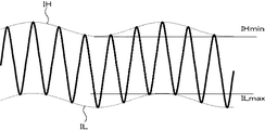
図14は、かかる2層BDのBCAマークの再生信号の波形(トラッキングサーボ制御を行っていない場合)の一例を示す。結晶状態では、反射率が高いので、高レベルIHの再生信号が得られ、アモルファス状態では、反射率が低いので、低レベルILの再生信号が得られる。 FIG. 14 shows an example of a waveform of a reproduction signal of the BCA mark of such a two-layer BD (when tracking servo control is not performed). Since the reflectance is high in the crystalline state, a high level IH reproduction signal is obtained, and in the amorphous state, the reflectance is low, and thus a low level IL reproduction signal is obtained.
しかしながら、従来の高密度光ディスク例えばBDにおいては、トラッキングサーボ制御がなされない場合には、再生レーザビームが複数のグルーブを跨がってBCAマークを読み取り、グルーブによる回折で信号が変調されることにより、グルーブ信号のクロストークより、図14に示すように、BCAマークの再生信号にレベルの変動が生じ、BCAマークの信号再生が不安定になる欠点があった。 However, in a conventional high-density optical disc such as a BD, when tracking servo control is not performed, the reproduction laser beam reads a BCA mark across a plurality of grooves, and the signal is modulated by diffraction by the grooves. Due to the crosstalk of the groove signal, as shown in FIG. 14, the level of the BCA mark reproduction signal varies, and the signal reproduction of the BCA mark becomes unstable.
BDの規格では、BCAマークを安定に再生するための基準として、BCAマークの再生信号の高レベルIHと低レベルILの比IH/IL(コントラストと称される)が4倍以上であることが規定されている。図14に示すように、レベル変動が大きな場合には、高レベルの最小値IHminと低レベルの最大値ILmaxとの比が上述した規格の値を満たすことが困難となる。 In the BD standard, as a standard for stably reproducing the BCA mark, the ratio IH / IL (referred to as contrast) between the high level IH and the low level IL of the reproduction signal of the BCA mark is 4 times or more. It is prescribed. As shown in FIG. 14, when the level fluctuation is large, it becomes difficult for the ratio between the high level minimum value IHmin and the low level maximum value ILmax to satisfy the above-mentioned standard value.
したがって、この発明の目的は、最内周側エリアに予め記録されている2進情報を安定に再生することを可能とする記録媒体およびその製造方法、並びに記録媒体用原盤およびその製造方法を提供することにある。 Accordingly, an object of the present invention is to provide a recording medium and a manufacturing method thereof, and a recording medium master and a manufacturing method thereof that can stably reproduce binary information recorded in advance in the innermost peripheral area. There is to do.
上述の課題を解決するために、この発明の第1の発明は、
第1の領域に第1のグルーブが形成され、第2の領域に第2のグルーブが形成された基板と、
基板上に形成された少なくとも2層以上の情報層と、
情報層上に形成された透明保護層と
を備え、
第1の領域は、媒体に固有の情報が記録される固有情報記録領域であり、
第2の領域は、データ記録領域であり、
第1の領域には、固有の情報が予め所定の2値情報として記録されており、
2値情報は、複数の第1のグルーブを横断して半径方向に延びるマークにより記録されており、
第1のグルーブの深さが第2のグルーブの深さに比して浅く、または第1のグルーブの幅が第2のグルーブの幅に比して狭くされた記録媒体である。
In order to solve the above-mentioned problem, the first invention of the present invention is:
A substrate having a first groove formed in a first region and a second groove formed in a second region;
At least two information layers formed on a substrate;
A transparent protective layer formed on the information layer,
The first area is a unique information recording area in which information unique to the medium is recorded,
The second area is a data recording area,
The first area, specific information is recorded in advance as a predetermined binary information,
The binary information is recorded by marks extending in the radial direction across the plurality of first grooves,
In the recording medium, the depth of the first groove is shallower than the depth of the second groove, or the width of the first groove is narrower than the width of the second groove.
この発明の第2の発明は、
樹脂材料に対してスタンパの転写面の形状を転写して基板を成形する工程と、
基板上に少なくとも2層以上の情報層を形成する工程と、
情報層上に透明保護層を形成する工程と
を備え、
スタンパは、
基板の第1の領域に対して第1のグルーブを形成する第1のスタンパグルーブと、
基板の第2の領域に対して第2のグルーブを形成する第2のスタンパグルーブと
を備え、
第1の領域は、媒体に固有の情報が記録される固有情報記録領域であり、
第2の領域は、データ記録領域であり、
第1の領域には、固有の情報が予め所定の2値情報として記録されており、
2値情報は、複数の第1のグルーブを横断して半径方向に延びるマークにより記録されており、
第1のスタンパグルーブの深さが、第2のスタンパグルーブの深さに比して浅く、または第1のスタンパグルーブの幅が、第2のスタンパグルーブの幅に比して狭くされた記録媒体の製造方法である。
The second invention of this invention is:
A step of molding the substrate by transferring the shape of the transfer surface of the stamper to the resin material;
Forming at least two information layers on a substrate;
Forming a transparent protective layer on the information layer,
The stamper
A first stamper groove forming a first groove with respect to a first region of the substrate;
A second stamper groove forming a second groove with respect to a second region of the substrate,
The first area is a unique information recording area in which information unique to the medium is recorded,
The second area is a data recording area,
The first area, specific information is recorded in advance as a predetermined binary information,
The binary information is recorded by marks extending in the radial direction across the plurality of first grooves,
Recording medium in which the depth of the first stamper groove is shallower than the depth of the second stamper groove, or the width of the first stamper groove is narrower than the width of the second stamper groove It is a manufacturing method.
この発明では、第1の領域のグルーブの深さおよび幅を第2の領域のグルーブに比してより浅くまたはより狭く形成しているので、第1の領域のグルーブによる回折で信号が変調されることを低減できる。すなわち、第1の領域の2値情報の再生信号に発生するレベルの変動を低減できる。 In the present invention, since the depth and width of the groove in the first region are formed shallower or narrower than the groove in the second region, the signal is modulated by diffraction by the groove in the first region. Can be reduced. That is, it is possible to reduce level fluctuations that occur in the binary information reproduction signal in the first region.
以上説明したように、この発明によれば、第1の領域のグルーブの深さおよび幅を第2の領域のグルーブに比してより浅くまたはより狭く形成することによって、第1の領域のグルーブによる回折を小さくし、2進情報の再生を良好に行うことができる。 As described above, according to the present invention, by the depth and width of the groove of the first region relative to the grooves of the second region shallower or narrower than forming a groove in the first region Therefore, the binary information can be reproduced well.
(1)発明の概要
以下、この発明の理解を容易とするために、この発明の概要について2層のBDを例として説明する。
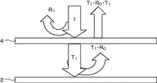
まず、図1を参照して、L0層2およびL1層4の反射率の関係について説明する。
L0層2およびL1層4からの反射光量が等しいと仮定すると、以下の関係式が成立する。
R1=T1・R0・T1 ・・・(1)
但し、R0:L0層2の反射率、R1:L1層4の反射率、T1:L1層4の透過率
(1) Outline of the Invention In order to facilitate understanding of the present invention, the outline of the present invention will be described below using a two-layer BD as an example.
First, the relationship between the reflectances of the
Assuming that the amount of reflected light from the
R 1 = T 1 · R 0 · T 1 (1)
Where R 0 : reflectance of the
そして、L0層2およびL1層4の熱吸収量が等しい、すなわち感度が等しいと仮定すると、以下の関係式が成立する。
1−R1−T1=T1−T1・R0 ・・・(2)
Then, assuming that the heat absorption amounts of the
1−R 1 −T 1 = T 1 −T 1 · R 0 (2)
(1)および(2)の式からT1を消去すると、
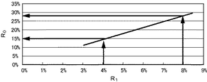
R0=((R1+1)2±√((R1+1)4−16R1 2))/2R1 ・・・(3)
となる。
ここで、0≦R0≦1であることより複合の「−」のみが解となる。そこで、式(3)の反射率R1と反射率R0の関係をグラフで表すと、図2のようになる。
反射率とコントラストは多重干渉の計算により図3のような関係になる。これは、反射率を上げようとするとコントラストが減少するということを表している。
If T 1 is eliminated from the equations (1) and (2),
R 0 = ((R 1 +1) 2 ± √ ((R 1 +1) 4 -16R 1 2 )) / 2R 1 (3)
It becomes.
Here, since 0 ≦ R 0 ≦ 1, only the complex “−” is the solution. Therefore, the relationship between the reflectivity R 1 and the reflectivity R 0 in equation (3) is represented by a graph as shown in FIG.
The reflectance and contrast have a relationship as shown in FIG. 3 by calculation of multiple interference. This indicates that the contrast decreases when the reflectance is increased.
一方、規格によれば、反射率R1は4%〜8%の範囲内であることが要求されるため、反射率R0の範囲は15%〜28%となる。したがって、設計では、その中心付近である20%近辺を用いることになる。 On the other hand, according to the standard, the reflectance R 1 is required to be in the range of 4% to 8%, so the range of the reflectance R 0 is 15% to 28%. Therefore, in the design, the vicinity of 20% that is near the center is used.
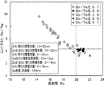
次に、表1および図4を参照して、コントラストRc/Ra(Rc:結晶状態の反射率、Ra:アモルファス状態の反射率)および反射率Rcの関係について説明する。 Next, with reference to Table 1 and FIG. 4, the relationship between the contrast Rc / Ra (Rc: reflectance in the crystalline state, Ra: reflectance in the amorphous state) and the reflectance Rc will be described.
ここで、これらの関係を求めるため用いたサンプルの構成について説明する。
サンプルは、基板上に、Ag合金層(反射層)、SiN層(第2の誘電体層)、ZnS−SiO2層(第1の誘電体層)、SbTe系相変化記録層(相変化記録層)、SiN層(第1の誘電体層)、ZnS−SiO2層(第2の誘電体層)、SiN層(第3の誘電体層)を順次積層した構成を有する。各サンプルの膜厚およびSb/Te比は、表1に示すように変化させた。
Here, the configuration of the sample used for obtaining these relationships will be described.
A sample is composed of an Ag alloy layer (reflection layer), a SiN layer (second dielectric layer), a ZnS-SiO 2 layer (first dielectric layer), an SbTe-based phase change recording layer (phase change recording) on a substrate. Layer), a SiN layer (first dielectric layer), a ZnS-SiO 2 layer (second dielectric layer), and a SiN layer (third dielectric layer) are sequentially laminated. The film thickness and Sb / Te ratio of each sample were changed as shown in Table 1.
表1は、各層の膜厚、L0層2のSb/Te比、反射率およびコントラストRc/Raなどを示す。図4は、表1に基づいて作成されたコントラストRc/Raおよび反射率Rcの関係を示すグラフである。
Table 1 shows the film thickness of each layer, the Sb / Te ratio of the
表1の反射率・コントラストの評価欄において、「○」は、反射率Rcが20%以上であり、且つコントラストRc/Raが4.4以上である場合を示し、「△」は、Rc>20%、4<Rc/Ra<4.4を示し、「×」は、これらの数値範囲を満たさない場合を示している。なお、表1では、製造マージンなどを考慮して、コントラストRc/Raが4.4以上である場合を良好と判断して「○」としているが、コントラストRc/Raが4以上でも規格を満足することは可能である。 In the reflectance / contrast evaluation column of Table 1, “◯” indicates the case where the reflectance Rc is 20% or more and the contrast Rc / Ra is 4.4 or more, and “Δ” indicates that Rc> 20%, 4 <Rc / Ra <4.4 is shown, and “x” indicates a case where these numerical ranges are not satisfied. In Table 1, in consideration of the manufacturing margin and the like, the case where the contrast Rc / Ra is 4.4 or more is judged as “good”, and “◯” is given. However, even when the contrast Rc / Ra is 4 or more, the standard is satisfied. It is possible to do.

上述のように、規格値である反射率R1=4%〜8%の範囲を満たすためには、L0層2の反射率R0としては20%程度の反射率が要求される。一方、規格によれば、コントラストIH/IL、すなわちコントラストRc/Raを4以上とすることが要求される。
As described above, in order to satisfy the standard value of the reflectance R 1 = 4% to 8%, the reflectance R 0 of the
しかしながら、図4に示すように、各層の膜厚および組成を調整しても、規格上求められる反射率(R0)20%、およびコントラスト(Rc/Ra)4を同時に大幅に上回ることはできず、反射率(R0)20%程度、コントラスト(Rc/Ra)4程度しか得られない。その理由は、コントラストと反射率は多重干渉の計算が示すごとく、相反する性質を持つからである。そのため、図3に示すグルーブによる回折の影響を抑え、変調度を最大化することが本発明の趣旨である。 However, as shown in FIG. 4, even if the film thickness and composition of each layer are adjusted, the reflectance (R0) of 20% and the contrast (Rc / Ra) of 4 that are required in the standard cannot be significantly exceeded at the same time. Only a reflectance (R 0 ) of about 20% and a contrast (Rc / Ra) of about 4 can be obtained. The reason is that contrast and reflectivity have contradictory properties as indicated by multiple interference calculations. Therefore, the gist of the present invention is to suppress the influence of diffraction by the groove shown in FIG. 3 and maximize the modulation degree.
したがって、上述のように、グルーブ信号の回折によりBCA再生信号が不安定である場合には(図14)、コントラストIH/ILが4以上という規格を満足できなくなる。そこで、本発明では、BCAにおけるグルーブの深さをデータ記録領域に比して浅くすることで、BCA再生信号を安定して再生できるようにする。 Therefore, as described above, when the BCA reproduction signal is unstable due to diffraction of the groove signal (FIG. 14), the standard that the contrast IH / IL is 4 or more cannot be satisfied. Therefore, in the present invention, the BCA reproduction signal can be stably reproduced by making the groove depth in the BCA shallower than the data recording area.
(2)光ディスクの構成
以下、この発明の一実施形態について図面を参照しながら説明する。図5は、この発明の一実施形態による光ディスクの構成の一例を示す。図6は、この発明の一実施形態による光ディスクのより具体的な構成の一例を示す。図7は、この発明の一実施形態による光ディスクの具体的な膜構成の一例を示す。
(2) Configuration of Optical Disc An embodiment of the present invention will be described below with reference to the drawings. FIG. 5 shows an example of the configuration of an optical disc according to an embodiment of the present invention. FIG. 6 shows an example of a more specific configuration of the optical disc according to one embodiment of the present invention. FIG. 7 shows an example of a specific film configuration of an optical disc according to an embodiment of the present invention.
この光ディスクは、基板1上に、L0層2、中間層3、L1層4、カバー層5が順次に積層された構成を有する2層の高密度光ディスクである。L0層2は、基板1上に、反射層6a、下層誘電体層7a、相変化記録層8a、上層誘電体層9aを順次積層してなる。L1層4は、中間層3上に、反射層6b、下層誘電体層7b、相変化記録層8b、上層誘電体層9bを順次積層してなる。
This optical disc is a two-layer high-density optical disc having a configuration in which an
この光ディスクは、中央に開口が設けられた円板状の形状を有し、L0層2には、その内周側から外周側に向かってBCA11、PIC(ディスクの制御データ)領域、データ記録領域が設定され、L1層2には、その内周側から外周側に向かって内周領域、PIC領域、データ記録領域が設定されている。
This optical disc has a disc shape with an opening in the center. The
この光ディスクでは、カバー層5側から情報記録層であるL0層2およびL1層4にレーザ光を照射することによって、情報信号の記録および再生が行われる。例えば、400nm〜410nmの波長を有するレーザ光が0.84〜0.86の開口数を有する対物レンズ10により集光され、カバー層5側から、情報記録層であるL0層2およびL1層4の一方に照射されることで、情報信号の記録または再生が行われる。このような光ディスクとしては、例えば2層BDが挙げられる。
以下、光ディスクを構成する基板1、L0層2、L1層4、中間層3、カバー層5について順次説明する。
In this optical disc, information signals are recorded and reproduced by irradiating the
Hereinafter, the
(基板)
基板1は、中央に開口(以下、センターホールと称する)が形成された円環形状を有する。この基板1の一主面は、凹凸面となっており、この凹凸面上にL0層2が成膜される。以下では、凹凸面のうちレーザ光入射面Sから遠い凹部をイングルーブGin、凹凸面のうちレーザ光入射面Sから近い凸部をオングルーブGonと称する。なお、基板1のBCA11に設けられた凸状のオングルーブGonが、第1のグルーブの一例であり、基板1のデータ記録領域13に設けられた凸状のオングルーブGonが、第2のグルーブの一例である。
(substrate)
The
この凹状のイングルーブGinおよび凸状のオングルーブGonの形状としては、例えば、スパイラル状、同心円状などの各種形状が挙げられる。また、イングルーブGinおよび/またはオングルーブGonが、アドレス情報を付加するためにウォブル(蛇行)されている。 Examples of the shape of the concave in-groove Gin and the convex on-groove Gon include various shapes such as a spiral shape and a concentric circle shape. The in-groove Gin and / or the on-groove Gon are wobbled (meandered) to add address information.
BCA11のオングルーブGonの幅dは、データ記録領域13のオングルーブGonの幅dに比べて狭く、および/または、BCA11のオングルーブGonの深さ(高さ)hは、データ記録領域13のオングルーブGonの深さ(高さ)hに比べて浅く(低く)なっている。また、BCA11とデータ記録領域13とでは隣り合うオングルーブGon間の距離、すなわちトラックピッチTpが異なっており、BCA11のトラックピッチTpはデータ記録領域13のトラックピッチTpに比べて広くなっている。このようにすることで、オングルーブGonによる回折でBCA信号が変調されることを低減できる。すなわち、BCAマークの再生信号におけるレベルの変動を低減できる。すなわち、コントラストIH/ILを向上させることができる。
The width d of the on-groove Gon of the
オングルーブGonの位相深さλ/αn(但し、λ:記録または再生のレーザ光の波長、α:グルーブ深さの係数、n:記録または再生のレーザ光に対する中間層の屈折率)がλ/304.8n〜λ/16.4nの範囲内であることが好まく、より好ましくはλ/304.8n〜λ/65.3nの範囲内である。このような範囲内にすることで、コントラストIH/ILを向上させることができるからである。 The phase depth λ / αn of the on-groove Gon (where λ: wavelength of recording or reproducing laser light, α: coefficient of groove depth, n: refractive index of the intermediate layer with respect to recording or reproducing laser light) is λ / It is preferably within the range of 304.8n to λ / 16.4n, and more preferably within the range of λ / 304.8n to λ / 65.3n. This is because the contrast IH / IL can be improved by setting it within such a range.
オングルーブGonの深さhは、0.9nm〜16.7nmの範囲内であることが好ましく、より好ましくは0.9nm〜4.2nmの範囲内である。このような範囲内にすることで、コントラストIH/ILを向上することができるからである。 The depth h of the on-groove Gon is preferably in the range of 0.9 nm to 16.7 nm, and more preferably in the range of 0.9 nm to 4.2 nm. This is because the contrast IH / IL can be improved by setting it within such a range.
オングルーブGonの幅dは、55nm〜126nmの範囲内であることが好ましく、より好ましくは55nm〜95nmの範囲内である。このような範囲内にすることで、コントラストIH/ILを向上することができるからである。 The width d of the on-groove Gon is preferably in the range of 55 nm to 126 nm, and more preferably in the range of 55 nm to 95 nm. This is because the contrast IH / IL can be improved by setting it within such a range.
オングルーブGonの幅dとトラックピッチTpとの比(d/Tp)は、0.0275〜0.063の範囲内であることが好ましく、より好ましくは0.0275〜0.0475の範囲内である。このような範囲内にすることで、コントラストIH/ILを向上することができるからである。ここで、オングルーブGonの幅dは、レーザ光入射面Sの側におけるオングルーブGonの幅d1のうちの最大幅d1maxと、それとは反対の底部側におけるオングルーブGonの幅d2のうちの最小幅d2minとの平均値(d1max+d2min)/2である。 The ratio (d / Tp) between the width d of the on-groove Gon and the track pitch Tp is preferably in the range of 0.0275 to 0.063, more preferably in the range of 0.0275 to 0.0475. is there. This is because the contrast IH / IL can be improved by setting it within such a range. Here, the width d of the on-groove Gon is the maximum width d1max of the widths d1 of the on-grooves Gon on the laser light incident surface S side and the maximum of the width d2 of the on-grooves Gon on the bottom side opposite thereto. The average value (d1max + d2min) / 2 with the small width d2min.
基板1の直径は、例えば120mmに選ばれる。基板1の厚さは、剛性を考慮して選ばれ、好ましくは0.3mm以上1.3mm以下から選ばれ、より好ましくは0.6mm以上1.3mm以下から選ばれ、例えば1.1mmに選ばれる。また、センタホールの径(直径)は、例えば15mmに選ばれる。
The diameter of the
基板1の材料としては、ポリカーボネート系樹脂、ポリオレフィン系樹脂もしくはアクリル系樹脂などの樹脂材料またはガラスを使用できるが、コストなどの点を考慮すると、樹脂材料を使用することが好ましい。樹脂材料としては、例えばゼオネックス、ポリカーボネート(以下、PCと適宜略す)(屈折率1.59)を用いることができる。
As the material of the
基板1の成形方法は、所望の形状と光学的に十分な基板表面の平滑性が得られる方法であればよく、特に限定されるものではない。例えば、射出成形法(インジェクション法)、紫外線硬化樹脂を使うフォトポリマー(2P法)法を用いることができる。射出成形法では、作製したマザースタンパを、ディスク基板作製用の金型キャビティ内に配設し、ポリカーボネートの透明樹脂を注入することにより、信号形成面に形成されたL0層2のグルーブパターンに対応する微小な凹凸が転写された基板1が作製される。
The method for forming the
(L0層、L1層)
情報記録層であるL0層2およびL1層4は、基板1の凹凸上に成膜された記録膜などから構成される層をいう。L0層2は、反射層6a、第2の誘電体層52a、第1の誘電体層51a、相変化記録層8a、第1の誘電体層53a、第2の誘電体層54a、第3の誘電体層55aを基板1上に順次積層してなる積層膜である。
第2の誘電体層52a、第1の誘電体層53a、第3の誘電体層55aを構成する材料としては、例えばSiNを用いることができる。第1の誘電体層51aおよび第2の誘電体層54aを構成する材料としては、例えばZnS−SiO2を用いることができる。
(L0 layer, L1 layer)
The
As a material constituting the
相変化記録層8aを構成する材料としては、レーザ光の照射を受けて可逆的な状態変化を生じる相変化材料を用いることができる。かかる相変化材料としては、例えば、アモルファス状態と結晶状態との可逆的相変化を生じる共晶系相変化材料または化合物系相変化材料を用いることができ、反射率および結晶化速度の観点からすると、共晶系相変化材料を用いることが好ましい。
As a material constituting the phase
共晶系相変化材料としては、SbTe系の共晶系材料を用いることができる。また、この共晶系材料に、保存耐久性の向上、結晶化速度の調整、変調度の向上などを目的として、Ag,In,Geなどの添加元素を加えることが好ましい。例示するならば、Sb−Te、Ge−Sb−Te、In−Sb−Te、Ag−In−Sb−Te、Au−In−Sb−Te、Ge−Sb−Te−Pd、Ge−Sb−Te−Se、Ge−Sb−Te−Bi、Ge−Sb−Te−Co、Ge−Sb−Te−Auを含む系、またはこれらの系に窒素、酸素などのガス添加物を導入した系などを挙げることができる。 As the eutectic phase change material, an SbTe-based eutectic material can be used. Moreover, it is preferable to add an additive element such as Ag, In, or Ge to the eutectic material for the purpose of improving the storage durability, adjusting the crystallization speed, and improving the degree of modulation. For example, Sb—Te, Ge—Sb—Te, In—Sb—Te, Ag—In—Sb—Te, Au—In—Sb—Te, Ge—Sb—Te—Pd, Ge—Sb—Te. -A system containing Se, Ge-Sb-Te-Bi, Ge-Sb-Te-Co, Ge-Sb-Te-Au, or a system in which a gas additive such as nitrogen or oxygen is introduced into these systems. be able to.
反射層6aを構成する材料としては、例えば、Al、Ag、Au、Ni、Cr、Ti、Pd、Co、Si、Ta、W、Mo、Geなどの単体、またはこれらを主成分とする合金を挙げることができる。これらのうち、特にAl系、Ag系、Au系、Si系、Ge系の材料が実用性の面から好ましい。合金としては、例えばAl−Ti、Al−Cr、Al−Cu、Al−Mg−Si、Ag−Pd−Cu、Ag−Pd−Ti、Si−B等が好適に用いられる。これらの材料のうちから、光学特性および熱特性を考慮して設定することが好ましい。例えば、単波長領域においても高反射率を有する点を考慮すると、Al系またはAg系材料を用いることが好ましい。
As a material constituting the
L1層4は、第2の誘電体層52b、第1の誘電体層51b、相変化記録層8b、第1の誘電体層53b、第2の誘電体層54bを中間層3上に順次積層してなる。
The
第1の誘電体層51b,53bを構成する材料としては、例えばZnS−SiO2を用いることができる。第2の誘電体層52b,54bを構成する材料としては、例えばSiNを用いることができる。
As a material constituting the first
相変化記録層8bを構成する材料としては、レーザ光の照射を受けて可逆的な状態変化を生じる相変化材料を用いることができる。かかる相変化材料としては、例えば、アモルファス状態と結晶状態との可逆的相変化を生じる共晶系相変化材料または化合物系相変化材料を用いることができる。
As a material constituting the phase
反射層6bを構成する材料としては、例えば、Al、Ag、Au、Ni、Cr、Ti、Pd、Co、Si、Ta、W、Mo、Ge等の単体、またはこれらを主成分とする合金を挙げることができる。これらのうち、特にAl系、Ag系、Au系、Si系、Ge系の材料が実用性の面から好ましい。合金としては、例えばAl−Ti、Al−Cr、Al−Cu、Al−Mg−Si、Ag−Pd−Cu、Ag−Pd−Ti、Si−B等が好適に用いられる。これらの材料のうちから、光学特性および熱特性を考慮して設定することが好ましい。例えば、単波長領域においても高反射率を有する点を考慮すると、Al系またはAg系材料を用いることが好ましい。
As a material constituting the
(中間層)
基板1に形成されたL0層2上には、例えば、厚さ25μmを有する樹脂層としての中間層3が形成される。この中間層3は、透明性を有する樹脂材料からなり、このような材料としては、例えばポリカーボネート系樹脂、ポリオレフィン系樹脂若しくはアクリル系樹脂などのプラスチック材料を用いることができる。中間層3のカバー層5側となる面は、基板1と同様に、イングルーブGinおよびオングルーブGonからなる凹凸面となっている。この凹凸面上にL1層4が成膜される。
(Middle layer)
On the
中間層3は、例えば、L0層2上に平坦塗布した紫外線硬化樹脂に対して真空環境下で透明樹脂スタンパを押し当て、このスタンパの凹凸を紫外線硬化樹脂に対して転写し、紫外線を紫外線硬化樹脂に対して照射して硬化させる。
この中間層3においても、上述の基板1と同様に、凹凸面のうちレーザ光入射面Sから遠い凹部をイングルーブGin、凹凸面のうちレーザ光入射面Sから近い凸部をオングルーブGonと称する。なお、中間層に設けられた凸状のオングルーブGonが、第3のグルーブの一例である。
For example, the
In the
この凹状のイングルーブGinおよび凸状のオングルーブGonの形状としては、例えば、スパイラル状、同心円状などの各種形状が挙げられる。また、イングルーブGinおよび/またはオングルーブGonが、アドレス情報を付加するためにウォブル(蛇行)されている。
内周領域11’のオングルーブGonは、例えばデータ記録領域13のオングルーブGonと同一の形状を有している。すなわち、内周領域11’のオングルーブGonの幅d、深さ(高さ)hはそれぞれ、例えばデータ記録領域13のオングルーブGonの幅d、深さ(高さ)hと等しくなっている。また、中間層3の内周領域11’およびデータ記録領域13に設けられたイングルーブGin、オングルーブGonは、例えば、基板1のデータ記録領域13に設けられたもの同様の形状となっている。
Examples of the shape of the concave in-groove Gin and the convex on-groove Gon include various shapes such as a spiral shape and a concentric circle shape. The in-groove Gin and / or the on-groove Gon are wobbled (meandered) to add address information.
The on-groove Gon in the inner
また、内周領域11’とデータ記録領域13とでは、隣り合うオングルーブGon間の距離、すなわちトラックピッチTpが異なっており、BCA11のトラックピッチTpはデータ記録領域13のトラックピッチTpに比べて広くなっている。
Further, the inner
(カバー層)
中間層3上に形成されたL1層4上には、カバー層5が形成される。カバー層5は、光ディスクの保護を目的として、形成される。情報信号の記録再生は、例えば、レーザ光がカバー層5を通じて情報記録層に集光されることによって行われる。
(Cover layer)
A
カバー層5としては、例えば、接着層とPCシート、またはUVレジン、UVレジンとPCシートからなるものを用いることができる。カバー層5は、例えば、75μm程度の厚さを有し、例えば、厚さ20μmを有する接着層と、厚さ55μmを有するPCシートとからなる。
As the
(光ディスクの各領域)
次に、この発明の一実施形態による光ディスクに設けられたBCA、PIC領域、データ記録領域について説明する。
(Each optical disc area)
Next, the BCA, PIC area, and data recording area provided on the optical disc according to the embodiment of the present invention will be described.
図8は、この発明の一実施形態による光ディスクのL0層のグルーブ配置の一例を概念的に示すものである。ここでは、オングルーブGonがデータを記録するためのトラックとなる場合を例として説明する。また、図8では、図示を容易にするために、BCA11およびPIC領域12に設けられたオングルーブGonの幅と、データ記録領域13に設けられたオングルーブGonの幅とをほぼ同一にしているが、上述したように、BCA11に設けられたオングルーブGonの幅dは、PIC領域12およびデータ記録領域13に設けられたオングルーブGonの幅dに比して狭くなっている。
FIG. 8 conceptually shows an example of the groove arrangement of the L0 layer of the optical disc according to one embodiment of the present invention. Here, a case where the on-groove Gon is a track for recording data will be described as an example. In FIG. 8, for ease of illustration, the width of the on-groove Gon provided in the
最内周側のBCA11には、2000nmトラックピッチのグルーブの配列が形成され、その外側のPIC領域12には、350nmトラックピッチのウォブルグルーブの配列が形成され、さらに外側のデータ記録領域13には、320nmトラックピッチのウォブリンググルーブが形成される。これらの各領域に形成されているグルーブは、基板表面に1つの螺旋状に連なるように形成され、トラックピッチが変化する領域間にトラックピッチ切り換えのためのトラックピッチ遷移領域(図示を省略)が配されている。
The
BCA11は、半径r=21.3mm〜22.0mmの間に設けられ、BCA11にグルーブ状トラックが形成されている。トラックピッチは2000nmであり、十分に広い間隔となっている。BCA11には、BCAマーク14が記録されている。BCAマーク14は、シリアル番号、ロット番号などの2進情報をバーコード化したデータであり、光ディスクに固有の情報として著作権保護のために利用される。BCAマーク14は、BCA11の複数のグルーブを横断して半径方向に延びる帯状のマークが例えば1周にわたって形成されたものである。
The
BCAマーク14は、光ディスクの初期化時に記録される。光ディスクの初期化前の状態では、情報記録層であるL0層2およびL1層4はアモルファスの状態にあり、データ記録領域13については、領域全体に対してレーザ光を照射して初期化を行うことで、アモルファスから結晶の状態に変化させる初期化がなされる。初期化に際して、L0層2のBCA11の全体を初期化して結晶の状態にするのではなく、BCAマーク14に対応させて、所要の部分(図8における斜線を付した領域)についてのみレーザ光の照射を行って結晶状態とする。この工程の結果、L0層2のBCA11においては、円周方向に沿った所要幅のアモルファス状態のバー部分と、結晶状態のバー部分とのパターンによる、バーコード態様の情報記録が行われる。なお、L1層4のBCA11では、L0層2のようにバーコード態様の情報記録は行われず、例えば、領域全体に対してレーザ光を照射して初期化を行うことで、アモルファスから結晶の状態に変化させる初期化がなされる。
PIC領域12は、再生専用領域であり、半径r=22.4mm〜23.197mmの間に設けられ、PIC領域12には、矩形ウォブルグルーブの配列からなるグルーブトラックがトラックピッチ350nmで形成されている。矩形ウォブルグルーブの配列から情報が再生される。
The
The
データ記録領域13は、半径r=23.2mm〜58.5mmの間に設けられ、データ記録領域13に正弦波ウォブルグルーブが形成されている。トラックピッチは320nmであり、これはピッチを詰めることによりさらに長時間記録・再生が可能な大容量を得ることができるようにするためである。なお、実際にデータが記録されるのは半径r=24.0mmより外周側となる。
The
それぞれに適したグルーブを形成するために、各領域では制御信号が用いられる。制御信号は、BCA11のDCグルーブを形成する場合は、直流(DC)信号であり、PIC領域12の矩形ウォブルグルーブを形成する場合はバイフェーズ変調の矩形信号である。また、データ記録領域13のウォブルグルーブを形成する場合は956[kHz]のMSK(Minimum Shift Keying)と2倍波のSTW(Saw Tooth Wobble)の重畳信号を用いる。MSKとSTWの重畳信号はアドレスのウォブル情報を記録するものである。
In order to form a groove suitable for each, a control signal is used in each region. The control signal is a direct current (DC) signal when the DC groove of the
MSKとSTWの重畳ウォブルを用いるのは、MSK方式はS/N(Signal To Noise Ratio:信号対雑音比)に優れている反面、ウォブルシフトがある場合には検出が難しくなるという問題があるが、STWはウォブルシフトに強く、ほとんど劣化なく検出できることから、これらを組み合わせることで、確実なアドレス検出を検出できるようにしたためである。 The MSK and STW superimposed wobbles are used because the MSK method is excellent in S / N (Signal To Noise Ratio), but there is a problem that detection is difficult when there is a wobble shift. This is because the STW is resistant to wobble shift and can be detected with almost no deterioration, so that it is possible to detect reliable address detection by combining them.
書き換え型のBD−RE(Blu-ray Disk ReWritable)ディスクでは、合計56個のウォブルで「0」または「1」の1ビットを表現する。この56個を単位とし、ADIP(Address in pregroove)ユニットと呼ぶ。このADIPユニットを83個連続して読み出すと、1つのアドレスを示すADIPワードとなる。ADIPワードは、24ビット長のアドレス情報と12ビット長の補助データ、リファレンス(校正)領域、誤り訂正用データなどからなる。BD−REでは、メインデータを記録するRUB(Recording unit block,64Kバイト単位)1つあたりに3個のADIPワードが割り当てられる。 In a rewritable BD-RE (Blu-ray Disk ReWritable) disc, 1 bit of “0” or “1” is expressed by a total of 56 wobbles. These 56 units are referred to as ADIP (Address in pregroove) units. When 83 ADIP units are continuously read, an ADIP word indicating one address is obtained. The ADIP word includes 24-bit address information, 12-bit auxiliary data, a reference (calibration) area, error correction data, and the like. In the BD-RE, three ADIP words are assigned to each RUB (Recording unit block, 64 Kbyte unit) for recording main data.
(3)光ディスクの製造方法
次に、図9〜図11を参照しながら、上述のような構成を有する光ディスクの製造方法の一例について説明する。
(3) Optical Disk Manufacturing Method Next, an example of a method for manufacturing an optical disk having the above-described configuration will be described with reference to FIGS.
まず、例えばレーザ露光などによってL0マスタースタンパ61を作製する(図9A)。このL0マスタースタンパ61は、中央部に開口が形成された円環形状を有し、その一主面には溝が形成されている。以下では、L0マスタースタンパ61に設けられた溝、すなわち凹部をイングルーブGinと称し、イングルーブGinの間に設けられた凸部をオングルーブGonと称する。このイングルーブGinおよびオングルーブGonは、基板1のイングルーブGinおよびオングルーブGonと同一の形状を有する。
First, the
また、L0マスタースタンパ61の一主面には、上述した基板1と同様に、中央部から外周側に向かってBCA11、PIC領域(図示省略)、データ記録領域13が順次設けられている。BCA11のオングルーブGonの幅dは、データ記録領域13のオングルーブGonの幅dに比べて狭く、および/または、BCA11のオングルーブGonの深さhは、データ記録領域13のオングルーブGonの深さhに比べて浅くなっている。また、BCA11とデータ記録領域13とでは隣り合うオングルーブGon間の距離、すなわちトラックピッチTpが異なっており、BCA11におけるトラックピッチTpはデータ記録領域13におけるものに比べて広くなっている。
Further, similarly to the
次に、例えばMMS(master mother stamper)転写技術により、L0マスタースタンパ61から、その反転スタンパであるL0マザースタンパ62を作製する(図9B)。このL0マザースタンパ62の一主面には、L0マスタースタンパ61のオングルーブGon、イングルーブGinをそれぞれ反転させた形状であるオングルーブGon、イングルーブGinが設けられる。
Next, an L0 mother stamper 62 as an inversion stamper is produced from the
次に、L0マザースタンパ62を、例えば射出成形装置の金型に取り付け、射出成形により基板1を成形する(図9C)。
Next, the L0 mother stamper 62 is attached to, for example, a mold of an injection molding apparatus, and the
次に、例えばスパッタリング法により、反射層6a、下層誘電体層7a、相変化記録層8a、上層誘電体層9aを基板1上に順次積層する。これにより、基板1上にL0層2が形成される(図9D)。
Next, the
次に、例えばレーザ露光などによって、L1マスタースタンパ63を作製する(図10A)。このL0マスタースタンパ63は、中央部に開口が形成された円環形状を有し、その一主面には溝が形成されている。以下では、L1マスタースタンパ63に設けられた溝、すなわち凹部をイングルーブGinと称し、イングルーブGinの間に設けられた凸部をオングルーブGonと称する。このイングルーブGinおよびオングルーブGonは、中間層3のイングルーブGinおよびオングルーブGonと同一の形状を有する。
Next, the
また、L1マスタースタンパ63の一主面には、上述したL0マスタースタンパ61と同様に、中央部から外周側に向かって内周領域11’、PIC領域(図示省略)、データ記録領域13が順次設けられている。L1マスタースタンパ63の内周領域11’、データ記録領域13はそれぞれ、L0マスタースタンパ61のBCA11、データ記録領域13とほぼ同一半径領域にある。L1マスタースタンパ63の内周領域11’にあるイングルーブGin、オングルーブGonはそれぞれ、L1マスタースタンパ63のデータ記録領域にあるイングルーブGin、オングルーブGonとほぼ同一形状を有している。また、L1マスタースタンパ63の内周領域11’およびデータ記録領域13に設けられたイングルーブGin、オングルーブGonは、例えば、L0マスタースタンパ61のデータ記録領域13に設けられたものと同様の形状となっている。
Similarly to the
内周領域11’とデータ記録領域13とでは隣り合うオングルーブGon間の距離、すなわちトラックピッチTpが異なっており、内周領域11’のトラックピッチTpはデータ記録領域13のトラックピッチTpに比べて広くなっている。
The inner
次に、L1マスタースタンパ63を、例えば射出成形装置の金型に取り付け、射出成形によりL1樹脂スタンパ64を成形する(図10B)。
Next, the
次に、例えばスピンコート法により紫外線硬化樹脂を基板1上に均一に塗布する。その後、基板1上に均一に塗布された紫外線硬化樹脂に対して、L1樹脂スタンパ64のイングルーブGinおよびオングルーブGonを転写する。これにより、イングルーブGinおよびオングルーブGonが設けられた中間層3が形成される(図11A)。
Next, an ultraviolet curable resin is uniformly applied on the
次に、例えばスパッタリング法により、反射層6b、下層誘電体層7b、相変化記録層8b、上層誘電体層9bを基板1上に順次積層する。これにより、基板1上にL1層4が形成される(図11B)。
Next, the
次に、円環形状の光透過性シートを、例えばこのシートの一主面に予め均一に塗布された感圧性粘着剤(PSA:Pressure Sensitive Adhesive)を用いて、基板1の凹凸面側に貼り合わせる。これにより、L1層4上にカバー層5が形成される(図11C)。
以上により、目的とする光ディスクが得られる。
Next, an annular light transmissive sheet is attached to the uneven surface side of the
The target optical disc is obtained as described above.
以下、実施例によりこの発明を具体的に説明するが、この発明はこれらの実施例のみに限定されるものではない。なお、以下の実施例においては、上述の一実施形態と対応する部分には同一の符号を付す。 EXAMPLES Hereinafter, the present invention will be specifically described with reference to examples. However, the present invention is not limited to these examples. In the following examples, parts corresponding to those in the above-described embodiment are denoted by the same reference numerals.
図12は、ガラス原盤を作製するために用いた光学的記録装置の構成を示す略線図である。図13は、実施例の光ディスクの製造方法を説明するための断面図である。 FIG. 12 is a schematic diagram showing a configuration of an optical recording apparatus used for producing a glass master. FIG. 13 is a cross-sectional view for explaining an optical disk manufacturing method according to the embodiment.
(光学的記録装置)
まず、図12を参照して、ガラス原盤を作製するために用いた光学的記録装置(カッティッグ装置とも称される)について説明する。
(Optical recording device)
First, with reference to FIG. 12, an optical recording apparatus (also called a cutting apparatus) used for producing a glass master will be described.
この光学的記録装置は、レーザ光源21、移動光学テーブル25、ターンテーブル32、スピンドルサーボ33をその主要部として備えている。
The optical recording apparatus includes a
レーザ光源21は、記録媒体としてのガラス原盤41の表面に着膜されたレジスト層42を露光するための光源であり、例えば波長λ=266nmの記録用のレーザ光を発振するものである。ただし、露光用の光源としては、特にこのようなレーザ光源のみに限定されるものではない。このレーザ光源21より出射されたレーザ光は、平行ビームのまま直進し、ミラーM1およびミラーM2で反射されて向きを変えて、移動光学テーブル25へと導かれる。
The
移動光学テーブル25には、音響光学変調偏向器(AOM/AOD:Acoustic Optical Modulator/Acoustic Optical Deflector)23と2つのウェッジプリズム22とが配置されている。音響光学変調偏向器23およびウェッジプリズム22は、平行ビームのまま入射して来たレーザ光と音響光学変調偏向器23が作り出す格子面とがブラッグの条件を満たすと共に、ビーム水平高さが変わらないように配置されている。音響光学変調偏向器23に用いられる音響光学素子としては酸化テルル(TeO2)が好適である。
An acousto-optic modulation deflector (AOM / AOD) 23 and two
音響光学変調偏向器23には、所定の信号が駆動用ドライバ24から供給される。この信号は、BCA11において直線状のオングルーブGonを形成する場合には一定レベルのDC信号である。駆動用ドライバ24には、電圧周波数制御器(VCO:Voltage Controlled Oscillator)26から高周波信号が供給される。フォーマッタ27から電圧周波数制御器26には制御信号が供給される。
A predetermined signal is supplied from the driving
音響光学変調偏向器23は、ブラッグ回折における一次回折光強度が超音波パワーにほぼ比例することを利用したものであり、記録信号に基づいて超音波パワーを変調してレーザ光21の光変調を行う。ブラッグ回折を実現するために、ブラッグ条件;2dsinθ=nλ(d:格子間隔、λ:レーザ光波長、θ:レーザ光と格子面のなす角、n:整数)を満たすように、レーザ光の光軸に対する音響光学変調偏向器23の位置関係および姿勢を設定する。
The acousto-
また、電圧周波数制御器26からの制御信号は、BCA11では、直流(DC)信号が使用され、PIC領域12では、バイフェーズ変調の矩形信号が使用され、データ記録領域では、956[kHz]のMSK(Minimum Shift Keying)と2倍波のSTW(Saw Tooth Wobble)の重畳信号が使用される。
As the control signal from the voltage frequency controller 26, a direct current (DC) signal is used in the
上述のようにして変調および偏向されたレーザ光は、ミラーM3および対物レンズL2によりガラス原盤41のレジスト層42に照射され、所望のBCA11およびPIC領域12およびデータ記録領域13のそれぞれのオングルーブGonの潜像を形成する。
上述のような構成を有する光学的記録装置を用いて以下のような条件でカッティングを行った。
The laser light modulated and deflected as described above is applied to the resist
Cutting was performed using the optical recording apparatus having the above-described configuration under the following conditions.
この光学的記録装置では、BCA11における2000nmトラックピッチのオングルーブGonの配列からなるグルーブトラックと、PIC領域12における350nmトラックピッチの矩形ウォブルグルーブ(オングルーブGon)の配列からなるグルーブトラックと、データ記録領域13における正弦波ウォブルしたウォブリンググルーブ(オングルーブGon)であるグルーブトラックとが、1つの螺旋状に連なるパターンをガラス原盤41上のレジスト層42に形成した。
In this optical recording apparatus, a groove track composed of an on-groove Gon array having a 2000 nm track pitch in the
カッティング時には、トラックの長手方向の線速度が5.28[m/s]になるようにターンテーブル32の回転数を制御し、移動光学テーブル25の送りピッチを領域毎に変えて露光した。送りピッチはBCA11では、2.000μm(2000nm)とし、PIC領域12では0.350μm(350nm)とし、データ記録領域13では0.320μm(320nm)とした。
At the time of cutting, the rotation speed of the
なお、上述の光学的記録装置では、移動光学テーブル25の位置をポジションセンサ31によって検出し、それぞれの領域に対応したタイミングおよびピッチで露光を行って、上記のようなBCA11、PIC領域12およびデータ記録領域13のグルーブパターンの潜像をガラス原盤41上のレジストに露光することが可能である。
In the above-described optical recording apparatus, the position of the moving optical table 25 is detected by the
また、レーザスケール30により検知される波長(例えば0.78μm)を基準として、送りサーボ29およびエアスライダ28の動作を制御し、移動光学テーブル25の送りピッチを徐々に変化させた。
Further, the operation of the
BCA11(半径r=21.0mm〜22.0mm)の間は送りピッチ2000nmであり、BCA11およびPIC領域12間のトラックピッチ遷移領域(半径r=22.0mm〜22.4mm)で、送りピッチを2000nmから350nmに徐々に変化させた。PIC領域12(半径r=22.4mm〜23.197mm)の間は送りピッチ350nmであり、PIC領域12およびデータ記録領域13間のトラックピッチ遷移領域(半径r=23.197mm〜23.2mm)に送りピッチを350nmから320nmに徐々に変化させた。データ記録領域13(半径r=23.2mm〜58.5mm)では送りピッチ320nmでオングルーブGonを形成した。
The feed pitch is 2000 nm between BCA11 (radius r = 21.0 mm to 22.0 mm), and the feed pitch is changed in the track pitch transition region (radius r = 22.0 mm to 22.4 mm) between BCA11 and
次に、図示しない現像機を用いてレジスト基板の現像を行った。まず上述のようにしてオングルーブGonの潜像が形成されたレジスト基板40をレジスト層42が上部になるように現像機のターンテーブル32に載置して、水平面に対して回転させた。この後、レジスト層42上に現像液を滴下して、当該レジストを現像処理した。これにより、レジスト基板40が得られた。
Next, the resist substrate was developed using a developing machine (not shown). First, the resist
すなわち、上述の工程により、レジスト基板40が現像され、BCA11(2000nmトラックピッチ)のオングルーブGonと、PIC領域12(350nmトラックピッチ)の矩形ウォブルグルーブ(オングルーブGon)と、データ記録領域13(320nmトラックピッチ)におけるMSKとSTWの重畳したウォブリンググルーブ(オングルーブGon)とである各グルーブトラックが1つの螺旋状に連なった状態で、表面にパターニングされたレジスト基板40が得られた。
That is, the resist
次に、レジスト基板40の凹凸パターン上に、無電界メッキ法などによりニッケル皮膜でなる導電化膜層を形成した。次に、導電化膜層が形成されたレジスト基板を電鋳装置に取り付け、電気メッキ法により導電化膜層上に300μm程度の厚さになるようにニッケルメッキ層を形成した。
Next, a conductive film layer made of a nickel film was formed on the concavo-convex pattern of the resist
続いて、ニッケルメッキ層が形成されたガラス原盤41からニッケルメッキ層をカッターなどで剥離した。次に、剥離したニッケルメッキ層の信号形成面のレジストをアセトンなどを用いて洗浄し、スタンパ61を作製した後、凹凸が反転するマザースタンパ62を作製した。さらに、マザースタンパ62とポリカーボネート(屈折率1.59)の透明樹脂を用いて射出成形することにより、基板1を作製した。中間層3に対してL1層の凹凸パターンを転写するための樹脂スタンパ64も基板1と同様に作製した。
Subsequently, the nickel plating layer was peeled off from the
上述した基板1および樹脂スタンパ64を使用して図5に示すような2層BDを作製した。なお、この実施例においては、評価用ディスクである2層BDとして、表2に示すように、L0層のBCA11におけるオングルーブGonの深さおよび幅を変化させたものを作製した。
A two-layer BD as shown in FIG. 5 was produced using the
また、2層BDの膜構成は以下のようにした。
L0層2
反射層6a:Ag、140nm
第2の誘電体層52a:SiN、10nm
第1の誘電体層51a:ZnS−SiO2、10nm
相変化記録層8a:GeSbTe、10nm
第1の誘電体層53a:SiN、10nm
第2の誘電体層54a:ZnS−SiO2、30nm
第3の誘電体層55a:SiN、10nm
The film configuration of the two-layer BD was as follows.
First
Phase
First
L1層4
反射層6b:Ag、10nm
第2の誘電体層52b:SiN、10nm
第1の誘電体層51b:ZnS−SiO2、10nm
相変化記録層8b:GeSbTe、6nm
第1の誘電体層53b:ZnS−SiO2、10nm
第2の誘電体層55b:SiN、10nm
First
Phase
First dielectric layer 53b: ZnS—SiO 2 , 10 nm
Second dielectric layer 55b: SiN, 10 nm
中間層3は、紫外線硬化樹脂に対して樹脂スタンパ64を押し当て、紫外線硬化樹脂を硬化させることにより形成した。なお、中間層3の厚さは25μmとした。
The
カバー層5は、光透過性シートをPSAにより貼り合わせすることにより作製した。なお、カバー層5の厚さが75μmとなるように光透過シートおよびPSAの厚さを設定した。
The
次に、上述のようにして作製された2層BDについて、BCAマークの再生信号のIH/ILの特性を測定した。その測定結果を下記の表2に示す。BCAマークの再生は、波長406nm、NA=0.85である光ピックアップを備えた光ディスク評価機を用いて評価した。この評価機は5μm分解能のマグネスケールを備えており、アドレスの半径位置を正確に測定できる。なお、オングルーブGonの深さhおよび幅dは、情報記録層であるL0層2を被覆する前の基板1の段階のものであり、オングルーブGonの深さhは、基板1の表面からオングルーブGonの底部までの距離であり、オングルーブGonの幅dは、表面側の最大幅d1maxと底部側の最小幅d2minとの平均値(d1max+d2min)/2である。オングルーブGonの形状は、AFM(Atomic Force Microscope;原子間力顕微鏡)で測定した。
Next, the IH / IL characteristic of the reproduction signal of the BCA mark was measured for the two-layer BD manufactured as described above. The measurement results are shown in Table 2 below. The reproduction of the BCA mark was evaluated using an optical disk evaluator equipped with an optical pickup having a wavelength of 406 nm and NA = 0.85. This evaluator has a magnescale with a resolution of 5 μm and can accurately measure the radial position of the address. The depth h and the width d of the on-groove Gon are those at the stage of the
表2に示す測定結果には、BCA11がバンド1〜バンド7までに分割され、バンド1からバンド7に向かってカッティッグパワーを10%ずつ低下させた場合のオングルーブGonの深さと幅、並びにコントラスト(IH/IL)が示されている。また、表2におけるカッティングパワーは、グルーブを形成できる限界のレーザパワー(バンド7のレーザパワー)を基準にして百分率により表したものである。
In the measurement results shown in Table 2, the depth and width of the on-groove Gon when the
表2から分かるように、バンド1のカッティッグパワーが160%では、レジスト層42がガラス原盤41上まで除去され、オングルーブGonの断面形状がU字状となる。このグルーブの形状は、データ記録領域13におけるオングルーブGonと同様の形状である。バンド2(カッティッグパワー=150%)からバンド7(カッティッグパワー=100%)までの範囲では、IH/IL>4.0の規格が満たされている。すなわち、BCA11におけるBCAマークの再生を良好に行うことができる。
As can be seen from Table 2, when the cutting power of the
バンド2からバンド7までのカッティッグパワーでは、レジスト層42がガラス原盤41の表面が現れるまでは除去されず、オングルーブGonの断面形状がV字状となる。バンド5(カッティングパワー=120%)からバンド7(カッティッグパワー=100%)までの範囲では、IH/IL≧4.09となっている。すなわち、BCA11におけるBCAマークの再生をより良好に行うことができる。すなわち、より好ましくは、バンド5(カッティッグパワー=120%、IH/IL=4.09)、バンド6(カッティッグパワー=110%、IH/IL=4.10)、バンド7(カッティッグパワー=100%、IH/IL=4.12)である。
With the cutting power from
したがって、BCA11におけるカッティングパワーをデータ記録領域13に比して小さくすることが好ましい。具体的には、BCA11におけるカッティングパワーは150%〜100%の範囲内であることが好ましく、より好ましくは100%〜120%の範囲内である。
Therefore, it is preferable to reduce the cutting power in the
また、表2から分かるように、バンド2〜バンド7のオングルーブGonの深さhにすると、IH/IL>4.0の規格が満たされている。さらに、バンド2〜バンド7のオングルーブGonの深さhにすると、IH/IL≧4.09となる。
Further, as can be seen from Table 2, when the depth h of the on-groove Gon of the
したがって、オングルーブGonの深さhは、0.9nm〜16.7nmであることが好ましく、より好ましくは0.9nm〜4.2nmの範囲内である。この場合のバンド2〜バンド7のグルーブの位相深さλ/αnは、下記のものとなる。
Therefore, the depth h of the on-groove Gon is preferably 0.9 nm to 16.7 nm, and more preferably in the range of 0.9 nm to 4.2 nm. In this case, the phase depth λ / αn of the grooves of
λ/304.8n〜λ/16.4n (nは中間層の屈折率;1.48)
λ/304.8n(但し、α=406nm/(1.48×0.9[nm])=304.8)
λ/16.4n (但し、α=406nm/(1.48×16.7[nm])=16.4)
また、バンド5〜バンド7のオングルーブGonの位相深さλ/αnは、下記のものとなる。
λ / 304.8n to λ / 16.4n (n is the refractive index of the intermediate layer; 1.48)
λ / 304.8n (where α = 406 nm / (1.48 × 0.9 [nm]) = 304.8)
λ / 16.4n (where α = 406 nm / (1.48 × 16.7 [nm]) = 16.4)
Further, the phase depth λ / αn of the on-groove Gon of the
λ/304.8n〜λ/65.3n (nは中間層の屈折率;1.48)
λ/304.8n(但し、α=406nm/(1.48×0.9[nm])=304.8)
λ/65.3n (但し、α=406nm/(1.48×4.2[nm])=16.4)
λ / 304.8n to λ / 65.3n (n is the refractive index of the intermediate layer; 1.48)
λ / 304.8n (where α = 406 nm / (1.48 × 0.9 [nm]) = 304.8)
λ / 65.3n (where α = 406 nm / (1.48 × 4.2 [nm]) = 16.4)
また、表2から分かるように、バンド2〜バンド7のオングルーブGonの幅にすると、IH/IL>4.0の規格が満たされている。さらに、バンド5〜バンド7のオングルーブGonの幅にすると、IH/IL≧4.09となる。
Further, as can be seen from Table 2, when the width of the on-groove Gon of the
したがって、BCA11におけるオングルーブGonの幅は、55nm〜126nmであることが好ましく、より好ましくは55nm〜95nmの範囲内である。
Therefore, the width of the on-groove Gon in the
オングルーブGonの幅をトラックピッチで正規化すると、バンド2〜バンド7のオングルーブGonの幅d/トラックピッチTpは、下記の通りである。
0.0275〜0.063
0.0275(但し、55[nm]/2000[nm]=0.0275)
0.063 (但し、126[nm]/2000[nm]=0.063)
When the width of the on-groove Gon is normalized by the track pitch, the width d / track pitch Tp of the on-groove Gon of the
0.0275-0.063
0.0275 (however, 55 [nm] / 2000 [nm] = 0.0275)
0.063 (however, 126 [nm] / 2000 [nm] = 0.063)
また、バンド5〜バンド7のオングルーブGonの幅d/トラックピッチTpは、下記の通りである。
0.0275〜0.0475
0.0275(但し、55[nm]/2000[nm]=0.0275)
0.0475(但し、95[nm]/2000[nm]=0.0475)
Further, the width d / track pitch Tp of the on-groove Gon of the
0.0275-0.0475
0.0275 (however, 55 [nm] / 2000 [nm] = 0.0275)
0.0475 (however, 95 [nm] / 2000 [nm] = 0.0475)
上述したBCA11のオングルーブGonの形状のとき、IH/IL>4.0の規格を満たし、BCA11に記録されているバーコード信号を良好に再生することができる。
When the shape of the on-groove Gon of the
また、表2から分かるように、BCA11のオングルーブGonの深さh、幅dをデータ記録領域13のオングルーブGonに比して、より浅く且つより狭くすることにより、BCA11に記録されているバーコード信号を良好に再生することができる。
Further, as can be seen from Table 2, the depth h and width d of the on-groove Gon of the
また、BCA11のオングルーブGonの深さhをデータ記録領域13のオングルーブGonの深さhに比してより浅くし、BCA11のオングルーブGonの幅dをデータ記録領域13のオングルーブGonの幅dとほぼ等しくした場合にも、BCA11に記録されているバーコード信号を良好に再生することができる、という効果を得ることができる。
Further, the depth h of the on-groove Gon of the
また、BCA11のオングルーブGonの幅dをデータ記録領域13のオングルーブGonの幅dに比してより狭くし、BCA11のオングルーブGonの深さhをデータ記録領域13のオングルーブGonの深さhとほぼ等しくした場合にも、上述の効果を同様に得ることができる。
Further, the width d of the on-groove Gon of the
また、上述の結果から、2層BDより高密度または低密度の光ディスクであっても、位相深さλ/αn、オングルーブGonの幅dとトラックピッチTpとの比率(d/Tp)を上述の数値範囲にすることで、BCA11に記録されているバーコード信号を良好に再生することができることが分かる。
Further, from the above results, the phase depth λ / αn and the ratio (d / Tp) of the on-groove Gon width d to the track pitch Tp are described above even in the case of an optical disc having a higher or lower density than the two-layer BD. It can be seen that the bar code signal recorded in the
以上、この発明の一実施形態について具体的に説明したが、この発明は、上述の一実施形態に限定されるものではなく、この発明の技術的思想に基づく各種の変形が可能である。 The embodiment of the present invention has been specifically described above, but the present invention is not limited to the above-described embodiment, and various modifications based on the technical idea of the present invention are possible.
例えば、上述の一実施形態においては、内周から外周に螺旋状にフォーマットを記録形成する例について説明したが、逆に外周から内周にフォーマットを記録形成した時の送り精度が良好な場合は、2つの異なる情報層を外周から内周にフォーマットを記録形成しても良い。また、この発明は、2層に限らず、3層、4層などの多層フォーマットにも適用可能である。 For example, in the above-described embodiment, the example in which the format is recorded and formed spirally from the inner periphery to the outer periphery has been described. Two different information layers may be recorded and formed from the outer periphery to the inner periphery. In addition, the present invention is not limited to two layers but can be applied to a multilayer format such as three layers, four layers, and the like.
また、上述の一実施形態においては、書換可能型の光ディスクに対してこの発明を適用する場合を例として説明したが、この発明はこの例に限定されるものではなく、再生専用型および追記型の光ディスクに対しても適用可能である。 In the above-described embodiment, the case where the present invention is applied to a rewritable optical disk has been described as an example. However, the present invention is not limited to this example. The present invention is also applicable to other optical discs.
また、この発明はBD以外の種々の光ディスクに対しても適用可能であり、従来の光ディスクのみならず、BDなどの光ディスクよりも更に高密度の次世代の光ディスクに対しても適用可能である。 Further, the present invention can be applied to various optical disks other than the BD, and can be applied not only to a conventional optical disk but also to a next generation optical disk having a higher density than an optical disk such as a BD.
また、上述の一実施形態においては、有機レジストを用いて記録媒体用原盤を作製する場合を例として説明したが、無機レジストを用いて記録媒体用原盤を作製するようにしてもよい。 In the above-described embodiment, the case where the recording medium master is manufactured using the organic resist has been described as an example. However, the recording medium master may be manufactured using the inorganic resist.
また、上述の一実施形態では、第1の領域(BCA)が最内周側に設けられている場合について説明したが、第1の領域を設ける位置は最内周側に限定されるものではなく、最外周側、最内周および最外周の間の領域など光ディスクの任意の領域に設けることができる。 In the above-described embodiment, the case where the first area (BCA) is provided on the innermost peripheral side has been described. However, the position where the first area is provided is not limited to the innermost peripheral side. Instead, it can be provided in an arbitrary area of the optical disc such as an area between the outermost circumference side, the innermost circumference and the outermost circumference.
1・・・基板
2・・・L0層
3・・・中間層
4・・・L1層
5・・・カバー層
11・・・BCA
12・・・PIC領域
13・・・データ記録領域
21・・・光源
22・・・ウェッジプリズム
23・・・音響光学偏向器(AOD)
25・・・移動光学テーブル
26・・・電圧周波数制御器(VCO)
32・・・ガラス原盤
33・・・レジスト層
34・・・ターンテーブル
L2・・・対物レンズ
M1,M2,M3・・・ミラー
41・・・ガラス原盤
42・・・レジスト層
DESCRIPTION OF
DESCRIPTION OF
25 ... Moving optical table 26 ... Voltage frequency controller (VCO)
32 ...
Claims (12)
上記基板上に形成された少なくとも2層以上の情報層と、
上記情報層上に形成された透明保護層と
を備え、
上記第1の領域は、媒体に固有の情報が記録される固有情報記録領域であり、
上記第2の領域は、データ記録領域であり、
上記第1の領域には、上記固有の情報が予め所定の2値情報として記録されており、
上記2値情報は、複数の上記第1のグルーブを横断して半径方向に延びるマークにより記録されており、
上記第1のグルーブの深さが上記第2のグルーブの深さに比して浅く、または上記第1のグルーブの幅が上記第2のグルーブの幅に比して狭くされた記録媒体。 A substrate having a first groove formed in a first region and a second groove formed in a second region;
At least two information layers formed on the substrate;
A transparent protective layer formed on the information layer,
The first area is a unique information recording area in which information unique to the medium is recorded.
The second area is a data recording area,
Above the first region, the specific information is recorded in advance as a predetermined binary information,
The binary information is recorded by marks extending in the radial direction across the plurality of first grooves,
A recording medium in which the depth of the first groove is shallower than the depth of the second groove, or the width of the first groove is narrower than the width of the second groove.
上記情報層が相変化型記録層であり、上記所定の2値情報が上記情報層の初期化時に記録された記録媒体。 The recording medium according to claim 1,
A recording medium in which the information layer is a phase change recording layer and the predetermined binary information is recorded when the information layer is initialized.
上記情報層が、SbTe系共晶系材料からなる相変化型記録層である記録媒体。 The recording medium according to claim 1,
A recording medium in which the information layer is a phase change recording layer made of an SbTe eutectic material.
上記基板を成形するためのスタンパを作製するためのカッティッグ工程において、上記第1のグルーブに対応する露光用レーザのパワーを上記第2のグルーブに対応する露光用レーザのパワーに比してより小として製造された記録媒体。 The recording medium according to claim 1,
In the cutting step for producing the stamper for forming the substrate, the power of the exposure laser corresponding to the first groove is smaller than the power of the exposure laser corresponding to the second groove. Recording media manufactured as
上記第1のグルーブの深さが0.9〜16.7nmである記録媒体。 The recording medium according to claim 1,
A recording medium in which the depth of the first groove is 0.9 to 16.7 nm.
上記基板上に形成された第1の情報層と、
上記第1の情報層上に形成された透明中間層と、
上記透明中間層上に形成された第2の情報層と、
上記第2の情報層上に形成された上記透明保護層と
を備える記録媒体。 The recording medium according to claim 1,
A first information layer formed on the substrate;
A transparent intermediate layer formed on the first information layer;
A second information layer formed on the transparent intermediate layer;
A recording medium comprising: the transparent protective layer formed on the second information layer.
上記第1のグルーブの位相深さがλ/304.8n〜λ/16.4n(但し、λ:記録または再生のレーザ光の波長、n:記録または再生のレーザ光に対する透明中間層の屈折率)である記録媒体。 The recording medium according to claim 6,
The phase depth of the first groove is λ / 304.8n to λ / 16.4n (where λ is the wavelength of the recording or reproducing laser beam, n is the refractive index of the transparent intermediate layer with respect to the recording or reproducing laser beam) ) Is a recording medium.
上記第1のグルーブの幅が55〜126nmである記録媒体。 The recording medium according to claim 1,
A recording medium in which the width of the first groove is 55 to 126 nm.
上記第1のグルーブのグルーブ幅/トラックピッチが0.0275〜0.063である記録媒体。 The recording medium according to claim 1,
A recording medium in which the groove width / track pitch of the first groove is 0.0275 to 0.063.
上記2値情報は、バーコード状マークとして記録されている記録媒体。 The recording medium according to claim 1,
The binary information is a recording medium recorded as a barcode mark.
上記第1の領域が最内周領域であり、上記第2の領域がデータ記録領域である記録媒体。 The recording medium according to claim 1,
A recording medium in which the first area is an innermost peripheral area and the second area is a data recording area.
上記基板上に少なくとも2層以上の情報層を形成する工程と、
上記情報層上に透明保護層を形成する工程と
を備え、
上記スタンパは、
上記基板の第1の領域に対して第1のグルーブを形成する第1のスタンパグルーブと、
上記基板の第2の領域に対して第2のグルーブを形成する第2のスタンパグルーブと
を備え、
上記第1の領域は、媒体に固有の情報が記録される固有情報記録領域であり、
上記第2の領域は、データ記録領域であり、
上記第1の領域には、上記固有の情報が予め所定の2値情報として記録されており、
上記2値情報は、複数の上記第1のグルーブを横断して半径方向に延びるマークにより記録されており、
上記第1のスタンパグルーブの深さが、上記第2のスタンパグルーブの深さに比して浅く、または上記第1のスタンパグルーブの幅が、上記第2のスタンパグルーブの幅に比して狭くされた記録媒体の製造方法。 A step of molding the substrate by transferring the shape of the transfer surface of the stamper to the resin material;
Forming at least two information layers on the substrate;
Forming a transparent protective layer on the information layer,
The stamper is
A first stamper groove forming a first groove with respect to the first region of the substrate;
A second stamper groove forming a second groove with respect to the second region of the substrate,
The first area is a unique information recording area in which information unique to the medium is recorded.
The second area is a data recording area,
Above the first region, the specific information is recorded in advance as a predetermined binary information,
The binary information is recorded by marks extending in the radial direction across the plurality of first grooves,
The depth of the first stamper groove is shallower than the depth of the second stamper groove, or the width of the first stamper groove is narrower than the width of the second stamper groove. Manufacturing method of the recorded recording medium.
Priority Applications (7)
| Application Number | Priority Date | Filing Date | Title |
|---|---|---|---|
| JP2006308483A JP4770710B2 (en) | 2005-11-17 | 2006-11-14 | RECORDING MEDIUM AND ITS MANUFACTURING METHOD, RECORDING MEDIUM MASTER AND ITS MANUFACTURING METHOD |
| PCT/JP2006/323376 WO2007058375A1 (en) | 2005-11-17 | 2006-11-16 | Recording medium and its manufacturing method, and recording medium master and its manufacturing method |
| CN2006800051098A CN101120406B (en) | 2005-11-17 | 2006-11-16 | Recording medium, method for manufacturing the same, master for recording medium, and method for manufacturing the same |
| EP06823526A EP1950747A4 (en) | 2005-11-17 | 2006-11-16 | RECORDING MEDIUM AND METHOD OF MANUFACTURING THE SAME AND RECORDING MEDIUM MASTER AND METHOD OF MANUFACTURING THE SAME |
| US11/813,746 US8154981B2 (en) | 2005-11-17 | 2006-11-16 | Record medium, its manufacturing method, mother disc for record medium, and its manufacturing method |
| KR1020077016260A KR20080077042A (en) | 2005-11-17 | 2006-11-16 | Recording medium and its manufacturing method, and raw material for recording medium and its manufacturing method |
| TW095142621A TWI419157B (en) | 2005-11-17 | 2006-11-17 | A recording medium, a manufacturing method thereof, a recording medium master, and a method of manufacturing the same |
Applications Claiming Priority (3)
| Application Number | Priority Date | Filing Date | Title |
|---|---|---|---|
| JP2005333458 | 2005-11-17 | ||
| JP2005333458 | 2005-11-17 | ||
| JP2006308483A JP4770710B2 (en) | 2005-11-17 | 2006-11-14 | RECORDING MEDIUM AND ITS MANUFACTURING METHOD, RECORDING MEDIUM MASTER AND ITS MANUFACTURING METHOD |
Publications (2)
| Publication Number | Publication Date |
|---|---|
| JP2007164965A JP2007164965A (en) | 2007-06-28 |
| JP4770710B2 true JP4770710B2 (en) | 2011-09-14 |
Family
ID=38048750
Family Applications (1)
| Application Number | Title | Priority Date | Filing Date |
|---|---|---|---|
| JP2006308483A Expired - Fee Related JP4770710B2 (en) | 2005-11-17 | 2006-11-14 | RECORDING MEDIUM AND ITS MANUFACTURING METHOD, RECORDING MEDIUM MASTER AND ITS MANUFACTURING METHOD |
Country Status (7)
| Country | Link |
|---|---|
| US (1) | US8154981B2 (en) |
| EP (1) | EP1950747A4 (en) |
| JP (1) | JP4770710B2 (en) |
| KR (1) | KR20080077042A (en) |
| CN (1) | CN101120406B (en) |
| TW (1) | TWI419157B (en) |
| WO (1) | WO2007058375A1 (en) |
Families Citing this family (10)
| Publication number | Priority date | Publication date | Assignee | Title |
|---|---|---|---|---|
| DE60321321D1 (en) * | 2002-02-18 | 2008-07-10 | Matsushita Electric Industrial Co Ltd | EVER DRIVE |
| JP2009003993A (en) * | 2007-06-19 | 2009-01-08 | Sony Corp | RECORDING MEDIUM AND ITS MANUFACTURING METHOD, RECORDING MEDIUM MASTER AND ITS MANUFACTURING METHOD |
| JP2010067313A (en) * | 2008-09-10 | 2010-03-25 | Sanyo Electric Co Ltd | Optical disk and optical disk apparatus |
| JP4661953B2 (en) * | 2008-12-04 | 2011-03-30 | ソニー株式会社 | Optical recording medium and manufacturing method thereof |
| JP2010186541A (en) * | 2009-01-16 | 2010-08-26 | Sharp Corp | Optical information recording medium and device for recording/reproducing information on/from optical information recording medium |
| JP4702461B2 (en) | 2009-02-12 | 2011-06-15 | ソニー株式会社 | Optical recording medium |
| JP5372864B2 (en) | 2009-08-18 | 2013-12-18 | パナソニック株式会社 | Multilayer optical disk and optical disk apparatus |
| JP4806080B2 (en) * | 2010-02-18 | 2011-11-02 | 株式会社東芝 | Optical recording medium, information recording method, and information reproducing method |
| WO2011158617A1 (en) * | 2010-06-14 | 2011-12-22 | 三菱電機株式会社 | Laser processing device and laser processing method |
| JP5553718B2 (en) * | 2010-09-17 | 2014-07-16 | 富士フイルム株式会社 | Optical information recording medium |
Family Cites Families (16)
| Publication number | Priority date | Publication date | Assignee | Title |
|---|---|---|---|---|
| JP3528989B2 (en) * | 1995-01-20 | 2004-05-24 | ソニー株式会社 | Data multiplexing device, data multiplexing method, multiplexed data processing device, and multiplexed data processing method |
| JP3652017B2 (en) * | 1995-08-23 | 2005-05-25 | 三井化学株式会社 | Optical recording medium |
| DE60042503D1 (en) | 1999-07-15 | 2009-08-13 | Panasonic Corp | Recording method for optical recording medium |
| JP2001243636A (en) | 1999-07-15 | 2001-09-07 | Matsushita Electric Ind Co Ltd | Optical recording medium and recording method for optical recording medium |
| US6973020B2 (en) * | 2000-04-17 | 2005-12-06 | Matsushita Electric Industrial Co., Ltd. | Recording medium, method and apparatus for reproducing, and method and apparatus for recording |
| JP2002050053A (en) * | 2000-08-01 | 2002-02-15 | Tdk Corp | Optical information medium |
| CN1220981C (en) * | 2001-10-15 | 2005-09-28 | 日本胜利株式会社 | information record carrier |
| JP2003281739A (en) * | 2001-10-15 | 2003-10-03 | Victor Co Of Japan Ltd | Information record carrier |
| EP1324326B1 (en) * | 2001-12-18 | 2005-11-30 | Matsushita Electric Industrial Co., Ltd. | Information recording medium and method for producing the same |
| JP4101666B2 (en) | 2002-01-22 | 2008-06-18 | 松下電器産業株式会社 | Information recording medium, recording apparatus, reproducing apparatus, recording method, reproducing method |
| DE60321321D1 (en) | 2002-02-18 | 2008-07-10 | Matsushita Electric Industrial Co Ltd | EVER DRIVE |
| JP2003272238A (en) * | 2002-03-19 | 2003-09-26 | Sony Corp | Optical recording / reproducing medium, master for producing optical recording / reproducing medium, and optical recording / reproducing apparatus |
| US7177262B2 (en) | 2002-04-19 | 2007-02-13 | Victor Company Of Japan, Ltd. | Reproducing system and corresponding information recording medium having wobbled land portions |
| JP3714331B2 (en) * | 2003-02-14 | 2005-11-09 | ソニー株式会社 | Optical recording medium, master for manufacturing optical recording medium, recording / reproducing apparatus, and recording / reproducing method |
| JP2004342216A (en) * | 2003-05-15 | 2004-12-02 | Sony Corp | Optical recording medium, master for producing optical recording medium, recording / reproducing apparatus and recording / reproducing method |
| TWI348695B (en) | 2003-12-08 | 2011-09-11 | Panasonic Corp | Optical information recording medium and method for manufacturing the medium |
-
2006
- 2006-11-14 JP JP2006308483A patent/JP4770710B2/en not_active Expired - Fee Related
- 2006-11-16 EP EP06823526A patent/EP1950747A4/en not_active Withdrawn
- 2006-11-16 CN CN2006800051098A patent/CN101120406B/en not_active Expired - Fee Related
- 2006-11-16 KR KR1020077016260A patent/KR20080077042A/en not_active Ceased
- 2006-11-16 WO PCT/JP2006/323376 patent/WO2007058375A1/en not_active Ceased
- 2006-11-16 US US11/813,746 patent/US8154981B2/en not_active Expired - Fee Related
- 2006-11-17 TW TW095142621A patent/TWI419157B/en not_active IP Right Cessation
Also Published As
| Publication number | Publication date |
|---|---|
| TW200739573A (en) | 2007-10-16 |
| WO2007058375A1 (en) | 2007-05-24 |
| US20090129252A1 (en) | 2009-05-21 |
| EP1950747A4 (en) | 2009-01-28 |
| CN101120406B (en) | 2010-12-08 |
| CN101120406A (en) | 2008-02-06 |
| US8154981B2 (en) | 2012-04-10 |
| KR20080077042A (en) | 2008-08-21 |
| JP2007164965A (en) | 2007-06-28 |
| TWI419157B (en) | 2013-12-11 |
| EP1950747A1 (en) | 2008-07-30 |
Similar Documents
| Publication | Publication Date | Title |
|---|---|---|
| JP4150155B2 (en) | Information recording medium, information recording method, reproducing method, recording / recording apparatus, and information reproducing apparatus | |
| US7952985B2 (en) | Recording medium, its manufacturing method, mother disc for recording medium, and its manufacturing method | |
| JP4770710B2 (en) | RECORDING MEDIUM AND ITS MANUFACTURING METHOD, RECORDING MEDIUM MASTER AND ITS MANUFACTURING METHOD | |
| JP4596752B2 (en) | Recording apparatus and recording method | |
| JP5189830B2 (en) | Information recording medium and master exposure apparatus | |
| JP4337080B2 (en) | Optical information recording medium | |
| JP4491803B2 (en) | Optical information recording medium | |
| JP4491802B2 (en) | Optical information recording medium | |
| JP4491804B2 (en) | Optical information recording medium | |
| JP4491807B2 (en) | Optical information recording medium | |
| JP4491806B2 (en) | Optical information recording medium | |
| CN1319054C (en) | Optical information recording medium and its producing process | |
| JP4370756B2 (en) | Optical recording / reproducing medium, master for producing optical recording / reproducing medium, method for producing optical recording / reproducing medium, and optical recording / reproducing apparatus | |
| TWI376691B (en) | Recording medium, its manufacturing method, mother disc for recording medium, and its manufacturing method | |
| JP2009170095A (en) | Optical information recording medium | |
| JP4396230B2 (en) | Optical recording method, master for manufacturing optical recording medium, and optical recording medium | |
| JP4600434B2 (en) | Optical information recording medium | |
| JP3986702B2 (en) | Optical recording medium and substrate for optical recording medium | |
| JP2006012355A (en) | Recording medium manufacturing method, recording medium, recording medium master manufacturing method, and recording medium master | |
| JP2007287320A (en) | Optical recording medium and method for determining recording conditions thereof | |
| JP2008010079A (en) | Write-once multilayer optical disc, recording method, reproduction method, and optical disc apparatus | |
| JP2006048785A (en) | Optical disc stamper manufacturing method, optical disc stamper and optical disc | |
| JP2005203051A (en) | Optical disc, optical disc master and recording method | |
| JP2007287318A (en) | Optical recording medium | |
| JP2007287319A (en) | Optical recording medium |
Legal Events
| Date | Code | Title | Description |
|---|---|---|---|
| A621 | Written request for application examination |
Free format text: JAPANESE INTERMEDIATE CODE: A621 Effective date: 20091102 |
|
| A131 | Notification of reasons for refusal |
Free format text: JAPANESE INTERMEDIATE CODE: A131 Effective date: 20100803 |
|
| A521 | Request for written amendment filed |
Free format text: JAPANESE INTERMEDIATE CODE: A523 Effective date: 20101004 |
|
| A131 | Notification of reasons for refusal |
Free format text: JAPANESE INTERMEDIATE CODE: A131 Effective date: 20101102 |
|
| A521 | Request for written amendment filed |
Free format text: JAPANESE INTERMEDIATE CODE: A523 Effective date: 20101105 |
|
| A02 | Decision of refusal |
Free format text: JAPANESE INTERMEDIATE CODE: A02 Effective date: 20110111 |
|
| A521 | Request for written amendment filed |
Free format text: JAPANESE INTERMEDIATE CODE: A523 Effective date: 20110411 |
|
| A911 | Transfer to examiner for re-examination before appeal (zenchi) |
Free format text: JAPANESE INTERMEDIATE CODE: A911 Effective date: 20110419 |
|
| TRDD | Decision of grant or rejection written | ||
| A01 | Written decision to grant a patent or to grant a registration (utility model) |
Free format text: JAPANESE INTERMEDIATE CODE: A01 Effective date: 20110524 |
|
| A01 | Written decision to grant a patent or to grant a registration (utility model) |
Free format text: JAPANESE INTERMEDIATE CODE: A01 |
|
| A61 | First payment of annual fees (during grant procedure) |
Free format text: JAPANESE INTERMEDIATE CODE: A61 Effective date: 20110606 |
|
| FPAY | Renewal fee payment (event date is renewal date of database) |
Free format text: PAYMENT UNTIL: 20140701 Year of fee payment: 3 |
|
| R151 | Written notification of patent or utility model registration |
Ref document number: 4770710 Country of ref document: JP Free format text: JAPANESE INTERMEDIATE CODE: R151 |
|
| FPAY | Renewal fee payment (event date is renewal date of database) |
Free format text: PAYMENT UNTIL: 20140701 Year of fee payment: 3 |
|
| R250 | Receipt of annual fees |
Free format text: JAPANESE INTERMEDIATE CODE: R250 |
|
| R250 | Receipt of annual fees |
Free format text: JAPANESE INTERMEDIATE CODE: R250 |
|
| R250 | Receipt of annual fees |
Free format text: JAPANESE INTERMEDIATE CODE: R250 |
|
| R250 | Receipt of annual fees |
Free format text: JAPANESE INTERMEDIATE CODE: R250 |
|
| R250 | Receipt of annual fees |
Free format text: JAPANESE INTERMEDIATE CODE: R250 |
|
| R250 | Receipt of annual fees |
Free format text: JAPANESE INTERMEDIATE CODE: R250 |
|
| R250 | Receipt of annual fees |
Free format text: JAPANESE INTERMEDIATE CODE: R250 |
|
| LAPS | Cancellation because of no payment of annual fees |