JP4768039B2 - 表示駆動装置および表示装置 - Google Patents
表示駆動装置および表示装置 Download PDFInfo
- Publication number
- JP4768039B2 JP4768039B2 JP2009048655A JP2009048655A JP4768039B2 JP 4768039 B2 JP4768039 B2 JP 4768039B2 JP 2009048655 A JP2009048655 A JP 2009048655A JP 2009048655 A JP2009048655 A JP 2009048655A JP 4768039 B2 JP4768039 B2 JP 4768039B2
- Authority
- JP
- Japan
- Prior art keywords
- switch
- voltage
- source line
- signal
- display
- Prior art date
- Legal status (The legal status is an assumption and is not a legal conclusion. Google has not performed a legal analysis and makes no representation as to the accuracy of the status listed.)
- Expired - Fee Related
Links
Images


Classifications
-
- G—PHYSICS
- G09—EDUCATION; CRYPTOGRAPHY; DISPLAY; ADVERTISING; SEALS
- G09G—ARRANGEMENTS OR CIRCUITS FOR CONTROL OF INDICATING DEVICES USING STATIC MEANS TO PRESENT VARIABLE INFORMATION
- G09G3/00—Control arrangements or circuits, of interest only in connection with visual indicators other than cathode-ray tubes
- G09G3/20—Control arrangements or circuits, of interest only in connection with visual indicators other than cathode-ray tubes for presentation of an assembly of a number of characters, e.g. a page, by composing the assembly by combination of individual elements arranged in a matrix no fixed position being assigned to or needed to be assigned to the individual characters or partial characters
- G09G3/22—Control arrangements or circuits, of interest only in connection with visual indicators other than cathode-ray tubes for presentation of an assembly of a number of characters, e.g. a page, by composing the assembly by combination of individual elements arranged in a matrix no fixed position being assigned to or needed to be assigned to the individual characters or partial characters using controlled light sources
- G09G3/30—Control arrangements or circuits, of interest only in connection with visual indicators other than cathode-ray tubes for presentation of an assembly of a number of characters, e.g. a page, by composing the assembly by combination of individual elements arranged in a matrix no fixed position being assigned to or needed to be assigned to the individual characters or partial characters using controlled light sources using electroluminescent panels
- G09G3/32—Control arrangements or circuits, of interest only in connection with visual indicators other than cathode-ray tubes for presentation of an assembly of a number of characters, e.g. a page, by composing the assembly by combination of individual elements arranged in a matrix no fixed position being assigned to or needed to be assigned to the individual characters or partial characters using controlled light sources using electroluminescent panels semiconductive, e.g. using light-emitting diodes [LED]
- G09G3/3208—Control arrangements or circuits, of interest only in connection with visual indicators other than cathode-ray tubes for presentation of an assembly of a number of characters, e.g. a page, by composing the assembly by combination of individual elements arranged in a matrix no fixed position being assigned to or needed to be assigned to the individual characters or partial characters using controlled light sources using electroluminescent panels semiconductive, e.g. using light-emitting diodes [LED] organic, e.g. using organic light-emitting diodes [OLED]
- G09G3/3275—Details of drivers for data electrodes
- G09G3/3291—Details of drivers for data electrodes in which the data driver supplies a variable data voltage for setting the current through, or the voltage across, the light-emitting elements
-
- G—PHYSICS
- G09—EDUCATION; CRYPTOGRAPHY; DISPLAY; ADVERTISING; SEALS
- G09G—ARRANGEMENTS OR CIRCUITS FOR CONTROL OF INDICATING DEVICES USING STATIC MEANS TO PRESENT VARIABLE INFORMATION
- G09G2310/00—Command of the display device
- G09G2310/02—Addressing, scanning or driving the display screen or processing steps related thereto
- G09G2310/0264—Details of driving circuits
- G09G2310/027—Details of drivers for data electrodes, the drivers handling digital grey scale data, e.g. use of D/A converters
-
- G—PHYSICS
- G09—EDUCATION; CRYPTOGRAPHY; DISPLAY; ADVERTISING; SEALS
- G09G—ARRANGEMENTS OR CIRCUITS FOR CONTROL OF INDICATING DEVICES USING STATIC MEANS TO PRESENT VARIABLE INFORMATION
- G09G2330/00—Aspects of power supply; Aspects of display protection and defect management
- G09G2330/02—Details of power systems and of start or stop of display operation
- G09G2330/021—Power management, e.g. power saving
- G09G2330/023—Power management, e.g. power saving using energy recovery or conservation
-
- G—PHYSICS
- G09—EDUCATION; CRYPTOGRAPHY; DISPLAY; ADVERTISING; SEALS
- G09G—ARRANGEMENTS OR CIRCUITS FOR CONTROL OF INDICATING DEVICES USING STATIC MEANS TO PRESENT VARIABLE INFORMATION
- G09G3/00—Control arrangements or circuits, of interest only in connection with visual indicators other than cathode-ray tubes
- G09G3/20—Control arrangements or circuits, of interest only in connection with visual indicators other than cathode-ray tubes for presentation of an assembly of a number of characters, e.g. a page, by composing the assembly by combination of individual elements arranged in a matrix no fixed position being assigned to or needed to be assigned to the individual characters or partial characters
- G09G3/22—Control arrangements or circuits, of interest only in connection with visual indicators other than cathode-ray tubes for presentation of an assembly of a number of characters, e.g. a page, by composing the assembly by combination of individual elements arranged in a matrix no fixed position being assigned to or needed to be assigned to the individual characters or partial characters using controlled light sources
- G09G3/30—Control arrangements or circuits, of interest only in connection with visual indicators other than cathode-ray tubes for presentation of an assembly of a number of characters, e.g. a page, by composing the assembly by combination of individual elements arranged in a matrix no fixed position being assigned to or needed to be assigned to the individual characters or partial characters using controlled light sources using electroluminescent panels
- G09G3/32—Control arrangements or circuits, of interest only in connection with visual indicators other than cathode-ray tubes for presentation of an assembly of a number of characters, e.g. a page, by composing the assembly by combination of individual elements arranged in a matrix no fixed position being assigned to or needed to be assigned to the individual characters or partial characters using controlled light sources using electroluminescent panels semiconductive, e.g. using light-emitting diodes [LED]
- G09G3/3208—Control arrangements or circuits, of interest only in connection with visual indicators other than cathode-ray tubes for presentation of an assembly of a number of characters, e.g. a page, by composing the assembly by combination of individual elements arranged in a matrix no fixed position being assigned to or needed to be assigned to the individual characters or partial characters using controlled light sources using electroluminescent panels semiconductive, e.g. using light-emitting diodes [LED] organic, e.g. using organic light-emitting diodes [OLED]
- G09G3/3225—Control arrangements or circuits, of interest only in connection with visual indicators other than cathode-ray tubes for presentation of an assembly of a number of characters, e.g. a page, by composing the assembly by combination of individual elements arranged in a matrix no fixed position being assigned to or needed to be assigned to the individual characters or partial characters using controlled light sources using electroluminescent panels semiconductive, e.g. using light-emitting diodes [LED] organic, e.g. using organic light-emitting diodes [OLED] using an active matrix
Description
この発明は、上記従来の課題を解決するものであり、電荷の再利用を行い省電力化を図ると共に、発熱を低減する表示駆動装置および表示装置を提供することを目的とする。
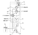
図1、図2は、本発明の第1の実施形態に係る表示装置、表示駆動装置の構成例を示すものである。
第1の実施形態では切り替え期間において全ソースライン45を短絡させて外部電源48に接続する例を説明した。つづいて、第2の実施形態では、切り替え期間において一部のソースライン45を短絡させて外部電源48に接続する表示制御部の構成について説明する。
第1および第2の実施形態では、外部電源48から供給される中間電圧は1種類である。これに対して、第3の実施形態では、ソースラインにドライブすべき画素信号の電圧範囲が色によって異なる場合に、色毎に最適な中間電圧を供給する構成について説明する。
第1の実施形態では、切り替え期間において、外部電源48は各第1スイッチsw1の一端に常に接続され、(A)各第1スイッチsw1がオンすることによりソースライン45同士が短絡するタイミングと、(B)各第2スイッチsw2がオフすることによりソースライン45と駆動部44とが切断されるタイミングと、(C)各ソースライン45に中間圧が印加されるタイミングとが同時に起こる構成について説明した。これに対して、第4の実施形態では、(A)および(B)のタイミングよりも(C)のタイミングを遅らせる構成について説明する。(C)のタイミングを遅らせるのは、ノイズの発生を回避し、貫通電流を防止するためである。
以上、図面を用いて説明したように、本発明の第1〜第4の実施形態に係る表示駆動装置および表示装置は、反転駆動を行わない表示装置、たとえば有機ELにおいても、電荷再利用の実現が可能となり、かつ電源を外部に持つことによる発熱対策も出来、多出力化が実現でき、低コスト化につながる。
また、データとの比較を行うことで、たとえばIC内部で閉じた効率的な電荷再利用を実現でき、無駄な消費電力を抑えることが出来る。
以下、本発明の実施形態における表示装置および表示駆動装置との比較例として、反転駆動をしない表示装置および表示駆動装置において本発明を適用しない場合の構成および動作を図面を参照しながら説明する。
有機ELパネル11に複数存在するゲートライン16のうちの3ラインの信号レベル状態をゲート信号1、ゲート信号2、ゲート信号3とする。また有機ELパネル11に複数存在するソースライン15のうちの2ラインの信号レベル状態をソース信号1、ソース信号2とする。また、それぞれのソース信号の出力範囲の中間電位を破線で表す。また、ゲート信号1の立ち上がりをt31、ゲート信号2の立ち上がりをt32、ゲート信号3の立ち上がりをt33とする。
データ信号として伝送される画像データは、データ取込信号によって第1ラッチ24に取り込まれる。この動作は、ソースドライバ13を構成するIC内のすべての駆動部14に対し順に行われる。すべての駆動部14に所望の画像データが第1ラッチ24の取り込まれた後、図15に示すデータ転送信号の立ち上がりt31に同期して第2ラッチ25にデータ転送される。第2ラッチ25に転送された画像データはセレクト部23へ接続され所望のアナログ電圧がAMP部22へ伝達され、ソースライン15へAMP部22によって電圧が出力される。この動作をライン毎に繰り返すことにより、ゲート信号がハイ区間の画素12に画像データに対応した電圧が印加され、順に全ラインへの電圧印加を繰り返すことにより、1フレームの表示がされる。
22 AMP部
23 セレクト部
24 第1ラッチ
25 第2ラッチ
41 有機ELパネル
42 画素
43 ソースドライバ
44 駆動部
45 ソースライン
46 ゲートライン
47 制御回路
48 外部電源
49 ゲートドライバ
51 制御回路
52 AMP部
53 セレクト部
54 第1ラッチ
55 第2ラッチ
73 ソースドライバ
74 駆動部
91 比較回路
96 比較器
97 ラッチ
98 アンドゲート
99 ナンドゲート
117 第1外部電源
118 第2外部電源
119 第3外部電源
111 第1ソースライン
112 第2ソースライン
113 第3ソースライン
123 ソースドライバ
128 制御回路
sw1 第1スイッチ
sw2 第2スイッチ
sw3 第3スイッチ
Claims (8)
- 画素列毎にソースラインを有する表示パネルを駆動する表示駆動装置であって、
ソースラインに画素信号を駆動するドライバと、
前記画素信号の最大電圧と最小電圧の間の電圧である中間電圧を中間電圧線に出力する電源部と、
前記中間電圧線に接続された第3スイッチと、
一端は前記第3スイッチに、他端は対応するソースラインに、接続された複数の第1スイッチと、
一端は前記ドライバに、他端は対応するソースラインおよび対応する前記第1スイッチの他端に接続された複数の第2スイッチと、
画素信号の出力期間と次の画素信号の出力期間との間の切り替え期間において、第2スイッチを一時的にオフにするとともに、当該第2スイッチに対応する前記第1スイッチを一時的にオンにして、第1スイッチをオンにした後に第3スイッチをオンにする制御部とを有する表示駆動装置。 - 前記ドライバ、第1スイッチ、第2スイッチおよび制御部は第1の半導体基板に形成され、前記電源部は第2の半導体基板に形成される請求項1に記載の表示駆動装置。
- 前記制御部は、前記切り替え期間において、全ての第2スイッチを一時的にオフにするとともに、当該第2スイッチに対応する全ての前記第1スイッチを一時的にオンにする
請求項1または2に記載の表示駆動装置。 - 前記中間電圧線は、第1のスイッチを介して第1の色に対応するソースラインに接続される第1電圧線と、第1のスイッチを介して第2の色に対応するソースラインに接続される第2電圧線とを含み、
前記電源部は、第1の色を表す画素信号の最大電圧と最小電圧の中間値である第1電圧を前記中間電圧として第1電圧線に出力し、第2の色を表す画素信号の最大電圧と最小電圧の中間値である第2電圧を前記中間電圧として第2電圧線に出力する
請求項1から3の何れかに記載の表示駆動装置。 - 請求項1から4までのいずれかに記載の表示駆動装置と、前記表示駆動装置によって駆動される表示パネルとを備える表示装置。
- 前記表示パネルは有機ELパネルである請求項5記載の表示装置。
- ソースラインに画素信号を駆動するためのドライバと、
前記画素信号の最大電圧と最小電圧の間の電圧である中間電圧を中間電圧線に出力する電源部と、
ソースラインに画素信号を駆動する時はドライバとソースラインを接続し、画素信号の切替期間にはソースラインとドライバを切り離し、前記ソースラインを他のソースラインと接続させた後、ソースラインと前記中間電圧線を接続する、制御部と、
を有する表示駆動装置。 - 前記ドライバ、および制御部は第1の半導体基板に形成され、前記電源部は第2の半導体基板に形成される請求項7に記載の表示駆動装置。
Priority Applications (3)
| Application Number | Priority Date | Filing Date | Title |
|---|---|---|---|
| JP2009048655A JP4768039B2 (ja) | 2009-03-02 | 2009-03-02 | 表示駆動装置および表示装置 |
| US12/713,689 US8456455B2 (en) | 2009-03-02 | 2010-02-26 | Display driving device and display apparatus |
| CN201010123948A CN101826292A (zh) | 2009-03-02 | 2010-03-02 | 显示驱动装置、显示装置 |
Applications Claiming Priority (1)
| Application Number | Priority Date | Filing Date | Title |
|---|---|---|---|
| JP2009048655A JP4768039B2 (ja) | 2009-03-02 | 2009-03-02 | 表示駆動装置および表示装置 |
Related Child Applications (2)
| Application Number | Title | Priority Date | Filing Date |
|---|---|---|---|
| JP2010233090A Division JP4755305B2 (ja) | 2010-10-15 | 2010-10-15 | 表示駆動装置 |
| JP2011012365A Division JP4848050B2 (ja) | 2011-01-24 | 2011-01-24 | 表示駆動装置 |
Publications (3)
| Publication Number | Publication Date |
|---|---|
| JP2010204312A JP2010204312A (ja) | 2010-09-16 |
| JP2010204312A5 JP2010204312A5 (ja) | 2010-10-28 |
| JP4768039B2 true JP4768039B2 (ja) | 2011-09-07 |
Family
ID=42666851
Family Applications (1)
| Application Number | Title | Priority Date | Filing Date |
|---|---|---|---|
| JP2009048655A Expired - Fee Related JP4768039B2 (ja) | 2009-03-02 | 2009-03-02 | 表示駆動装置および表示装置 |
Country Status (3)
| Country | Link |
|---|---|
| US (1) | US8456455B2 (ja) |
| JP (1) | JP4768039B2 (ja) |
| CN (1) | CN101826292A (ja) |
Families Citing this family (12)
| Publication number | Priority date | Publication date | Assignee | Title |
|---|---|---|---|---|
| KR101341912B1 (ko) * | 2009-09-25 | 2013-12-13 | 엘지디스플레이 주식회사 | 표시장치용 구동회로 |
| US9927891B2 (en) * | 2012-03-29 | 2018-03-27 | Synaptics Incorporated | System and method for reducing transmitter power consumption |
| JP5961125B2 (ja) * | 2013-02-26 | 2016-08-02 | 株式会社ジャパンディスプレイ | 表示装置及び電子機器 |
| CN103559860B (zh) * | 2013-08-16 | 2015-07-22 | 京东方科技集团股份有限公司 | 像素电路驱动电压调节方法及其调节装置、显示设备 |
| US9620057B2 (en) | 2013-08-16 | 2017-04-11 | Boe Technology Group Co., Ltd. | Method and apparatus for adjusting driving voltage for pixel circuit, and display device |
| KR20160022416A (ko) * | 2014-08-19 | 2016-03-02 | 삼성디스플레이 주식회사 | 표시 장치 및 이의 구동 방법 |
| CN106375553B (zh) * | 2016-08-24 | 2019-09-17 | 武汉华星光电技术有限公司 | 显示屏组合及具有该显示屏组合的移动终端 |
| WO2018079636A1 (ja) * | 2016-10-31 | 2018-05-03 | パナソニック株式会社 | 液晶表示装置及び故障検査方法 |
| JP6557369B2 (ja) * | 2018-01-30 | 2019-08-07 | ラピスセミコンダクタ株式会社 | ディスプレイ駆動装置 |
| CN110610678B (zh) | 2018-06-15 | 2022-02-01 | 深圳通锐微电子技术有限公司 | 驱动电路及显示装置 |
| US10991290B1 (en) * | 2020-10-07 | 2021-04-27 | Novatek Microelectronics Corp. | Control method of channel setting module applied to display panel |
| CN113257165B (zh) * | 2021-04-16 | 2022-09-20 | 深圳天德钰科技股份有限公司 | 数据驱动电路以及显示装置 |
Family Cites Families (16)
| Publication number | Priority date | Publication date | Assignee | Title |
|---|---|---|---|---|
| US7304632B2 (en) * | 1997-05-13 | 2007-12-04 | Oki Electric Industry Co., Ltd. | Liquid-crystal display driving circuit and method |
| KR100312344B1 (ko) | 1999-06-03 | 2001-11-03 | 최종선 | 다단계 전하 재활용을 이용한 tft-lcd 및 그 방법 |
| JP2002108284A (ja) | 2000-09-28 | 2002-04-10 | Nec Corp | 有機el表示装置及びその駆動方法 |
| JP2002229525A (ja) | 2001-02-02 | 2002-08-16 | Nec Corp | 液晶表示装置の信号線駆動回路及び信号線駆動方法 |
| JP2002366112A (ja) * | 2001-06-07 | 2002-12-20 | Hitachi Ltd | 液晶駆動装置及び液晶表示装置 |
| US7230597B2 (en) * | 2001-07-13 | 2007-06-12 | Tpo Hong Kong Holding Limited | Active matrix array devices |
| JP3951687B2 (ja) * | 2001-08-02 | 2007-08-01 | セイコーエプソン株式会社 | 単位回路の制御に使用されるデータ線の駆動 |
| JP4102309B2 (ja) | 2001-12-27 | 2008-06-18 | 株式会社ルネサステクノロジ | 表示駆動制御システム |
| FR2846454A1 (fr) | 2002-10-28 | 2004-04-30 | Thomson Licensing Sa | Dispositif de visualisation d'images a recuperation d'energie capacitive |
| JP2006065284A (ja) * | 2004-07-26 | 2006-03-09 | Seiko Epson Corp | 発光装置及び電子機器 |
| WO2007015348A1 (ja) * | 2005-08-04 | 2007-02-08 | Sharp Kabushiki Kaisha | 液晶表示装置およびその駆動方法 |
| US8089437B2 (en) * | 2006-09-20 | 2012-01-03 | Seiko Epson Corporation | Driver circuit, electro-optical device, and electronic instrument |
| US8009130B2 (en) * | 2006-11-06 | 2011-08-30 | Lg Display Co., Ltd. | Liquid crystal display device and method of driving the same |
| JP2008241832A (ja) * | 2007-03-26 | 2008-10-09 | Seiko Epson Corp | 液晶装置、画素回路、アクティブマトリクス基板、および電子機器 |
| JP4492694B2 (ja) * | 2007-12-20 | 2010-06-30 | セイコーエプソン株式会社 | 集積回路装置、電気光学装置及び電子機器 |
| JP5260141B2 (ja) | 2008-05-22 | 2013-08-14 | パナソニック株式会社 | 表示駆動装置、表示モジュールパッケージ、表示パネルモジュール及びテレビセット |
-
2009
- 2009-03-02 JP JP2009048655A patent/JP4768039B2/ja not_active Expired - Fee Related
-
2010
- 2010-02-26 US US12/713,689 patent/US8456455B2/en active Active
- 2010-03-02 CN CN201010123948A patent/CN101826292A/zh active Pending
Also Published As
| Publication number | Publication date |
|---|---|
| US20100220080A1 (en) | 2010-09-02 |
| CN101826292A (zh) | 2010-09-08 |
| US8456455B2 (en) | 2013-06-04 |
| JP2010204312A (ja) | 2010-09-16 |
Similar Documents
| Publication | Publication Date | Title |
|---|---|---|
| JP4768039B2 (ja) | 表示駆動装置および表示装置 | |
| KR102413158B1 (ko) | 표시 장치 및 이를 이용한 표시 패널의 구동 방법 | |
| US7643042B2 (en) | Display device and driving circuit for displaying | |
| US8836629B2 (en) | Image display apparatus and image display method | |
| JP2008292837A (ja) | 表示装置 | |
| JP2008026761A (ja) | 消費電力制御装置、画像処理装置、自発光表示装置、電子機器、消費電力制御方法及びコンピュータプログラム | |
| JP2006292899A (ja) | 液晶表示装置、液晶ドライバ、及び液晶表示パネルの駆動方法 | |
| KR102054409B1 (ko) | 소스 구동 회로 및 액정 디스플레이 패널 | |
| KR20160038194A (ko) | 데이터 구동 회로 및 이를 포함하는 표시 장치 | |
| KR102126549B1 (ko) | 평판 표시 장치 및 그의 구동 방법 | |
| JP2006195430A (ja) | 液晶表示装置のソースドライバ駆動方法 | |
| US20150015620A1 (en) | Drive device of display panel, display device including the same, and drive method of display panel | |
| US20080062102A1 (en) | Liquid crystal display device and control method used in same | |
| JP2008170842A (ja) | 電気光学装置、駆動回路および電子機器 | |
| US8860647B2 (en) | Liquid crystal display apparatus and source driving circuit thereof | |
| US20140192096A1 (en) | Liquid crystal display device | |
| JP4755305B2 (ja) | 表示駆動装置 | |
| JP2009103819A (ja) | 表示装置 | |
| JP4848050B2 (ja) | 表示駆動装置 | |
| JP2008170978A (ja) | 表示装置及びその駆動方法 | |
| US10770022B2 (en) | Source driver and a display driver integrated circuit | |
| JP2006267903A (ja) | アクティブマトリクス型表示装置 | |
| JP2012058692A (ja) | 液晶表示装置の駆動装置および液晶表示システム | |
| KR20160058361A (ko) | 표시 패널의 구동 방법 및 이를 수행하는 표시 장치 | |
| US20120212469A1 (en) | Display driving circuit and method |
Legal Events
| Date | Code | Title | Description |
|---|---|---|---|
| A521 | Request for written amendment filed |
Free format text: JAPANESE INTERMEDIATE CODE: A523 Effective date: 20100722 |
|
| A621 | Written request for application examination |
Free format text: JAPANESE INTERMEDIATE CODE: A621 Effective date: 20100722 |
|
| A871 | Explanation of circumstances concerning accelerated examination |
Free format text: JAPANESE INTERMEDIATE CODE: A871 Effective date: 20100722 |
|
| A975 | Report on accelerated examination |
Free format text: JAPANESE INTERMEDIATE CODE: A971005 Effective date: 20100806 |
|
| A131 | Notification of reasons for refusal |
Free format text: JAPANESE INTERMEDIATE CODE: A131 Effective date: 20100817 |
|
| A521 | Request for written amendment filed |
Free format text: JAPANESE INTERMEDIATE CODE: A523 Effective date: 20101015 |
|
| A131 | Notification of reasons for refusal |
Free format text: JAPANESE INTERMEDIATE CODE: A131 Effective date: 20101124 |
|
| A521 | Request for written amendment filed |
Free format text: JAPANESE INTERMEDIATE CODE: A523 Effective date: 20110124 |
|
| TRDD | Decision of grant or rejection written | ||
| A01 | Written decision to grant a patent or to grant a registration (utility model) |
Free format text: JAPANESE INTERMEDIATE CODE: A01 Effective date: 20110517 |
|
| A61 | First payment of annual fees (during grant procedure) |
Free format text: JAPANESE INTERMEDIATE CODE: A61 Effective date: 20110615 |
|
| R150 | Certificate of patent or registration of utility model |
Ref document number: 4768039 Country of ref document: JP Free format text: JAPANESE INTERMEDIATE CODE: R150 Free format text: JAPANESE INTERMEDIATE CODE: R150 |
|
| FPAY | Renewal fee payment (event date is renewal date of database) |
Free format text: PAYMENT UNTIL: 20140624 Year of fee payment: 3 |
|
| S111 | Request for change of ownership or part of ownership |
Free format text: JAPANESE INTERMEDIATE CODE: R313113 |
|
| R350 | Written notification of registration of transfer |
Free format text: JAPANESE INTERMEDIATE CODE: R350 |
|
| R250 | Receipt of annual fees |
Free format text: JAPANESE INTERMEDIATE CODE: R250 |
|
| LAPS | Cancellation because of no payment of annual fees |