JP4653752B2 - バッファにおける伝搬遅延及びプロセス及び温度の影響を低減する方法 - Google Patents
バッファにおける伝搬遅延及びプロセス及び温度の影響を低減する方法 Download PDFInfo
- Publication number
- JP4653752B2 JP4653752B2 JP2006533727A JP2006533727A JP4653752B2 JP 4653752 B2 JP4653752 B2 JP 4653752B2 JP 2006533727 A JP2006533727 A JP 2006533727A JP 2006533727 A JP2006533727 A JP 2006533727A JP 4653752 B2 JP4653752 B2 JP 4653752B2
- Authority
- JP
- Japan
- Prior art keywords
- current source
- switch
- control input
- pulse current
- higher value
- Prior art date
- Legal status (The legal status is an assumption and is not a legal conclusion. Google has not performed a legal analysis and makes no representation as to the accuracy of the status listed.)
- Expired - Fee Related
Links
Images
Classifications
-
- H—ELECTRICITY
- H03—ELECTRONIC CIRCUITRY
- H03K—PULSE TECHNIQUE
- H03K19/00—Logic circuits, i.e. having at least two inputs acting on one output; Inverting circuits
- H03K19/01—Modifications for accelerating switching
- H03K19/017—Modifications for accelerating switching in field-effect transistor circuits
- H03K19/01707—Modifications for accelerating switching in field-effect transistor circuits in asynchronous circuits
- H03K19/01721—Modifications for accelerating switching in field-effect transistor circuits in asynchronous circuits by means of a pull-up or down element
-
- H—ELECTRICITY
- H03—ELECTRONIC CIRCUITRY
- H03K—PULSE TECHNIQUE
- H03K17/00—Electronic switching or gating, i.e. not by contact-making and –breaking
- H03K17/16—Modifications for eliminating interference voltages or currents
-
- H—ELECTRICITY
- H03—ELECTRONIC CIRCUITRY
- H03K—PULSE TECHNIQUE
- H03K17/00—Electronic switching or gating, i.e. not by contact-making and –breaking
- H03K17/04—Modifications for accelerating switching
-
- H—ELECTRICITY
- H03—ELECTRONIC CIRCUITRY
- H03K—PULSE TECHNIQUE
- H03K17/00—Electronic switching or gating, i.e. not by contact-making and –breaking
- H03K17/14—Modifications for compensating variations of physical values, e.g. of temperature
-
- H—ELECTRICITY
- H03—ELECTRONIC CIRCUITRY
- H03K—PULSE TECHNIQUE
- H03K17/00—Electronic switching or gating, i.e. not by contact-making and –breaking
- H03K17/16—Modifications for eliminating interference voltages or currents
- H03K17/161—Modifications for eliminating interference voltages or currents in field-effect transistor switches
- H03K17/162—Modifications for eliminating interference voltages or currents in field-effect transistor switches without feedback from the output circuit to the control circuit
- H03K17/163—Soft switching
- H03K17/164—Soft switching using parallel switching arrangements
Landscapes
- Physics & Mathematics (AREA)
- Engineering & Computer Science (AREA)
- Computer Hardware Design (AREA)
- Computing Systems (AREA)
- General Engineering & Computer Science (AREA)
- Mathematical Physics (AREA)
- Logic Circuits (AREA)
- Electronic Switches (AREA)
- Pulse Circuits (AREA)
Description
Claims (10)
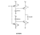
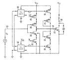
- 制御入力部を有する出力駆動トランジスタと、
反対の極性の、第1及び第2のより低値の電流源と、
オンの時には前記第1のより低値の電流源を前記制御入力部に接続する、第1のスイッチと、
オンの時には前記第2のより低値の電流源を前記制御入力部に接続する、第2のスイッチと、
反対の極性の、第1及び第2のより高値のパルス電流源であって、前記パルス電流源の両方が、前記制御入力部に接続されており、ここで、前記第1のパルス電流源は、前記第1のより低値の電流源と同じ極性であり、前記第2のパルス電流源は、前記第2のより低値の電流源と同じ極性であることからなる、第1及び第2のより高値のパルス電流源と、
前記第1のスイッチがオンに切り替えられる第1の状態と、前記第2のスイッチがオンに切り替えられる第2の状態とを有する、入力信号と、
前記入力信号のエッジ遷移によってアクティブにされるタイミング回路であって、前記より高値のパルス電流源の両方をアクティブにするための出力を有する、タイミング回路
とを備え、
前記第1のスイッチと前記第1のより高値のパルス電流源とが、実質的に同時に両方ともオンに切り替えられ、前記第2のスイッチと前記第2のより高値のパルス電流源とが、実質的に同時に両方ともオンに切り替えられることからなる、バッファ回路。 - 前記出力トランジスタが、MOSFETであり、前記制御入力部が、該MOSFETのゲートであることからなる、請求項1に記載のバッファ回路。
- 前記第1のより高値のパルス電流源は、
第3のより高値の電流源と、
オンの時には前記第3のより高値の電流源を前記制御入力部に接続する、第3のスイッチ
とを含み、及び、
前記第2のより高値のパルス電流源は、
第4のより高値の電流源と、
オンの時には前記第4のより高値の電流源を前記制御入力部に接続する、第4のスイッチ
とを含むことからなる、請求項1に記載のバッファ回路。 - 前記タイミング回路は、前記第3のスイッチを即座にオンに切り替える第1のワンショットタイミング回路と、前記第4のスイッチを即座にオンに切り替える第2のワンショットタイミング回路とを含むことからなる、請求項3に記載のバッファ回路。
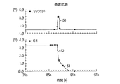
- 前記タイミング回路は、温度、プロセス、及び供給電圧の変動を補償するために構成され、
前記バッファ回路の遅延が、そのような変動にわたって実質的に一定のままとなることからなる、請求項1に記載のバッファ回路。 - 制御入力部を有する出力トランジスタを提供し、
反対の極性の、第1及び第2のより低値の電流源を、前記制御入力部に接続し、
反対の極性の、第1及び第2のより高値のパルス電流源を、前記制御入力部に接続し、
前記第1のスイッチがオンに切り替えられる第1の状態と、前記第2のスイッチがオンに切り替えられる第2の状態とを有する入力信号を提供し、及び、
前記入力信号のエッジ遷移によってタイミング回路をアクティブにし、前記より高値のパルス電流源の両方をトリガするための前記タイミング回路からの出力を提供する
ことを含み、
前記第1のより高値のパルス電流源が、前記第1のより低値の電流源と同じ極性であり、前記第2のより高値のパルス電流源が、前記第2のより低値の電流源と同じ極性であり、及び、
前記第1のより低値の電流源を前記接続することと、前記第1のより高値のパルス電流源を前記トリガすることとが、実質的に同時に起こり、及び、前記第2のより低値の電流源を前記接続することと、前記第2のより高値のパルス電流源を前記トリガすることとが、実質的に同時に起こることからなる、方法。 - 前記出力トランジスタが、MOSFETであり、前記制御入力部が、該MOSFETのゲートであることからなる、請求項6に記載の方法。
- 前記第1のより高値のパルス電流源を前記接続することが、
第3のより高値の電流源を提供し、及び、
前記第3のより高値の電流源を、第3のスイッチを介して前記制御入力部に接続する
ことを含み、
前記第2のより高値のパルス電流源を前記接続することが、
第4のより高値の電流源を提供し、及び、
前記第4のより高値の電流源を、第4のスイッチを介して前記制御入力部に接続する
ことを含むことからなる、請求項6に記載の方法。 - 前記第3のスイッチを即座にオンに切り替え、及び、前記第2のスイッチを即座にオンに切り替える
ことを更に含むことからなる、請求項8に記載の方法。 - 前記タイミング回路をアクティブにすることは、温度、プロセス、及び供給電圧の変動を補償し、
前記バッファ回路の遅延は、そのような変動にわたって、実質的に一定のままとなることからなる、請求項6に記載の方法。
Applications Claiming Priority (2)
| Application Number | Priority Date | Filing Date | Title |
|---|---|---|---|
| US10/460,075 US6756826B1 (en) | 2003-06-12 | 2003-06-12 | Method of reducing the propagation delay and process and temperature effects on a buffer |
| PCT/US2004/018605 WO2004112249A1 (en) | 2003-06-12 | 2004-06-10 | Method of reducing the propagation delay and process and temperature effects on a buffer |
Publications (2)
| Publication Number | Publication Date |
|---|---|
| JP2007517419A JP2007517419A (ja) | 2007-06-28 |
| JP4653752B2 true JP4653752B2 (ja) | 2011-03-16 |
Family
ID=32508108
Family Applications (1)
| Application Number | Title | Priority Date | Filing Date |
|---|---|---|---|
| JP2006533727A Expired - Fee Related JP4653752B2 (ja) | 2003-06-12 | 2004-06-10 | バッファにおける伝搬遅延及びプロセス及び温度の影響を低減する方法 |
Country Status (6)
| Country | Link |
|---|---|
| US (1) | US6756826B1 (ja) |
| JP (1) | JP4653752B2 (ja) |
| KR (1) | KR101099224B1 (ja) |
| CN (1) | CN100547925C (ja) |
| DE (1) | DE112004001029T5 (ja) |
| WO (1) | WO2004112249A1 (ja) |
Families Citing this family (13)
| Publication number | Priority date | Publication date | Assignee | Title |
|---|---|---|---|---|
| WO2003015101A2 (en) * | 2001-08-08 | 2003-02-20 | Koninklijke Philips Electronics N.V. | Random-access memory devices comprising a dioded buffer |
| JP2005045590A (ja) * | 2003-07-23 | 2005-02-17 | Mitsubishi Electric Corp | 半導体装置 |
| US7061301B2 (en) * | 2003-12-19 | 2006-06-13 | Power Integrations, Inc. | Method and apparatus switching a semiconductor switch with a multi-state drive circuit |
| KR100594322B1 (ko) * | 2005-02-14 | 2006-06-30 | 삼성전자주식회사 | 와이드 레인지 전원용 입력회로 |
| US7279997B2 (en) * | 2005-10-14 | 2007-10-09 | Freescale Semiconductor, Inc. | Voltage controlled oscillator with a multiple gate transistor and method therefor |
| US7256657B2 (en) * | 2005-10-14 | 2007-08-14 | Freescale Semiconductor, Inc. | Voltage controlled oscillator having digitally controlled phase adjustment and method therefor |
| US20070085576A1 (en) * | 2005-10-14 | 2007-04-19 | Hector Sanchez | Output driver circuit with multiple gate devices |
| US7411436B2 (en) * | 2006-02-28 | 2008-08-12 | Cornell Research Foundation, Inc. | Self-timed thermally-aware circuits and methods of use thereof |
| JP2012527178A (ja) | 2009-05-11 | 2012-11-01 | エスエス エスシー アイピー、エルエルシー | エンハンスメントモード型およびデプレションモード型のワイドバンドギャップ半導体jfetのためのゲートドライバ |
| KR101848757B1 (ko) * | 2011-12-08 | 2018-04-17 | 에스케이하이닉스 주식회사 | 반도체 장치 |
| CN104218924A (zh) * | 2014-09-01 | 2014-12-17 | 长沙景嘉微电子股份有限公司 | 一种应用于实时动态反馈环路的低毛刺电流开关电路 |
| JP6907662B2 (ja) * | 2017-04-04 | 2021-07-21 | 富士電機株式会社 | ゲート駆動回路およびこれを備えた負荷駆動装置 |
| GB202012559D0 (en) | 2020-08-12 | 2020-09-23 | Samsung Electronics Co Ltd | Reducing latency between receiving user input and displaying resulting frame |
Family Cites Families (12)
| Publication number | Priority date | Publication date | Assignee | Title |
|---|---|---|---|---|
| JPS59181828A (ja) * | 1983-03-31 | 1984-10-16 | Toshiba Corp | 半導体素子の出力バツフア回路 |
| US5557223A (en) * | 1993-06-08 | 1996-09-17 | National Semiconductor Corporation | CMOS bus and transmission line driver having compensated edge rate control |
| US5898315A (en) * | 1996-05-17 | 1999-04-27 | Cypress Semiconductor Corp. | Output buffer circuit and method having improved access |
| US6130563A (en) * | 1997-09-10 | 2000-10-10 | Integrated Device Technology, Inc. | Output driver circuit for high speed digital signal transmission |
| US6670822B2 (en) * | 1998-08-11 | 2003-12-30 | Fairchild Semiconductor Corporation | Transceiver driver with programmable edge rate control independent of fabrication process, supply voltage, and temperature |
| US6060938A (en) * | 1998-08-19 | 2000-05-09 | Fairchild Semiconductor Corp. | Output buffer for reducing switching noise |
| EP1050967B1 (de) * | 1999-05-07 | 2005-07-27 | Infineon Technologies AG | Schaltungsanordnung zur Ansteuerung eines Halbleiterschalters |
| US6268759B1 (en) * | 1999-11-23 | 2001-07-31 | Texas Instruments Incorporated | Low-power 5-volt input/output tolerant circuit with power-down control for a low voltage CMOS crossbar switch |
| US6335638B1 (en) * | 2000-06-29 | 2002-01-01 | Pericom Semiconductor Corp. | Triple-slope clock driver for reduced EMI |
| US6437622B1 (en) | 2001-03-27 | 2002-08-20 | Texas Instruments Incorporated | Temperature compensated slew rate control circuit |
| US20020177266A1 (en) * | 2001-05-24 | 2002-11-28 | Christian Klein | Selectable output edge rate control |
| US6535020B1 (en) * | 2001-12-18 | 2003-03-18 | Sun Microsystems, Inc. | Output buffer with compensated slew rate and delay control |
-
2003
- 2003-06-12 US US10/460,075 patent/US6756826B1/en not_active Expired - Fee Related
-
2004
- 2004-06-10 CN CNB2004800164487A patent/CN100547925C/zh not_active Expired - Fee Related
- 2004-06-10 DE DE112004001029T patent/DE112004001029T5/de not_active Ceased
- 2004-06-10 KR KR1020057023681A patent/KR101099224B1/ko not_active Expired - Fee Related
- 2004-06-10 WO PCT/US2004/018605 patent/WO2004112249A1/en not_active Ceased
- 2004-06-10 JP JP2006533727A patent/JP4653752B2/ja not_active Expired - Fee Related
Also Published As
| Publication number | Publication date |
|---|---|
| CN100547925C (zh) | 2009-10-07 |
| DE112004001029T5 (de) | 2006-06-08 |
| JP2007517419A (ja) | 2007-06-28 |
| US6756826B1 (en) | 2004-06-29 |
| CN1806388A (zh) | 2006-07-19 |
| WO2004112249A1 (en) | 2004-12-23 |
| KR20060059896A (ko) | 2006-06-02 |
| KR101099224B1 (ko) | 2011-12-27 |
Similar Documents
| Publication | Publication Date | Title |
|---|---|---|
| EP0329285B1 (en) | Output buffer | |
| US6590432B1 (en) | Low-voltage differential driver with opened eye pattern | |
| JP4653752B2 (ja) | バッファにおける伝搬遅延及びプロセス及び温度の影響を低減する方法 | |
| KR930007078A (ko) | 출력버퍼 구동회로 | |
| JP4111753B2 (ja) | データバッファ回路およびデータ出力バッファ | |
| CN108604898A (zh) | 实施缓冲晶体管的动态栅极偏置的输入/输出(i/o)驱动器 | |
| US5864244A (en) | Tristate buffer circuit with transparent latching capability | |
| US5306958A (en) | High-speed address transition detection circuit | |
| JPH07212212A (ja) | 出力バッファ回路 | |
| JP4137339B2 (ja) | 出力バッファ回路及び半導体装置 | |
| US6724224B1 (en) | Bus relay and voltage shifter without direction control input | |
| US8344763B2 (en) | Low-speed driver circuit | |
| US6366520B1 (en) | Method and system for controlling the slew rate of signals generated by open drain driver circuits | |
| US6014046A (en) | Off chip driver (OCD) with variable drive capability for noise control | |
| US5600261A (en) | Output enable access for an output buffer | |
| US6307414B1 (en) | Slew rate/propagation delay selection circuit | |
| KR100564562B1 (ko) | 오픈 드레인 방식의 출력단을 구동하는 출력 드라이버 | |
| US6777987B2 (en) | Signal buffer for high-speed signal transmission and signal line driving circuit including the same | |
| US6825694B2 (en) | Flip-flop circuit for use in electronic devices | |
| KR100500927B1 (ko) | 반도체소자의 출력버퍼 | |
| US5561634A (en) | Input buffer of semiconductor memory device | |
| KR100518234B1 (ko) | 출력 버퍼 회로 | |
| US7173475B1 (en) | Signal transmission amplifier circuit | |
| KR0157956B1 (ko) | 출력 버퍼회로 | |
| KR100250684B1 (ko) | 출력잡음에 의한 오동작을 배제하는 입력버퍼 |
Legal Events
| Date | Code | Title | Description |
|---|---|---|---|
| A621 | Written request for application examination |
Free format text: JAPANESE INTERMEDIATE CODE: A621 Effective date: 20070521 |
|
| A131 | Notification of reasons for refusal |
Free format text: JAPANESE INTERMEDIATE CODE: A131 Effective date: 20100413 |
|
| A601 | Written request for extension of time |
Free format text: JAPANESE INTERMEDIATE CODE: A601 Effective date: 20100707 |
|
| A602 | Written permission of extension of time |
Free format text: JAPANESE INTERMEDIATE CODE: A602 Effective date: 20100714 |
|
| A521 | Request for written amendment filed |
Free format text: JAPANESE INTERMEDIATE CODE: A523 Effective date: 20101008 |
|
| TRDD | Decision of grant or rejection written | ||
| A01 | Written decision to grant a patent or to grant a registration (utility model) |
Free format text: JAPANESE INTERMEDIATE CODE: A01 Effective date: 20101124 |
|
| A01 | Written decision to grant a patent or to grant a registration (utility model) |
Free format text: JAPANESE INTERMEDIATE CODE: A01 |
|
| A61 | First payment of annual fees (during grant procedure) |
Free format text: JAPANESE INTERMEDIATE CODE: A61 Effective date: 20101217 |
|
| R150 | Certificate of patent or registration of utility model |
Free format text: JAPANESE INTERMEDIATE CODE: R150 |
|
| FPAY | Renewal fee payment (event date is renewal date of database) |
Free format text: PAYMENT UNTIL: 20131224 Year of fee payment: 3 |
|
| R250 | Receipt of annual fees |
Free format text: JAPANESE INTERMEDIATE CODE: R250 |
|
| LAPS | Cancellation because of no payment of annual fees |