JP4628067B2 - インターポーザの接合方法、及び電子部品。 - Google Patents
インターポーザの接合方法、及び電子部品。 Download PDFInfo
- Publication number
- JP4628067B2 JP4628067B2 JP2004329658A JP2004329658A JP4628067B2 JP 4628067 B2 JP4628067 B2 JP 4628067B2 JP 2004329658 A JP2004329658 A JP 2004329658A JP 2004329658 A JP2004329658 A JP 2004329658A JP 4628067 B2 JP4628067 B2 JP 4628067B2
- Authority
- JP
- Japan
- Prior art keywords
- interposer
- base
- side terminal
- adhesive
- terminal
- Prior art date
- Legal status (The legal status is an assumption and is not a legal conclusion. Google has not performed a legal analysis and makes no representation as to the accuracy of the status listed.)
- Active
Links
- 238000000034 method Methods 0.000 title claims description 41
- 238000005304 joining Methods 0.000 title claims description 28
- 239000000853 adhesive Substances 0.000 claims description 108
- 230000001070 adhesive effect Effects 0.000 claims description 103
- 239000000463 material Substances 0.000 claims description 33
- 238000003825 pressing Methods 0.000 claims description 28
- 239000004033 plastic Substances 0.000 claims description 12
- 229920003023 plastic Polymers 0.000 claims description 12
- 238000010292 electrical insulation Methods 0.000 claims description 8
- 230000002093 peripheral effect Effects 0.000 claims description 6
- 229920001169 thermoplastic Polymers 0.000 claims description 5
- 239000004416 thermosoftening plastic Substances 0.000 claims description 5
- 238000010438 heat treatment Methods 0.000 claims description 4
- 238000013008 moisture curing Methods 0.000 claims description 4
- 238000004891 communication Methods 0.000 claims description 2
- 239000010410 layer Substances 0.000 description 15
- 230000015572 biosynthetic process Effects 0.000 description 6
- 239000004065 semiconductor Substances 0.000 description 6
- 238000004519 manufacturing process Methods 0.000 description 5
- RYGMFSIKBFXOCR-UHFFFAOYSA-N Copper Chemical compound [Cu] RYGMFSIKBFXOCR-UHFFFAOYSA-N 0.000 description 4
- 238000000576 coating method Methods 0.000 description 4
- 239000011888 foil Substances 0.000 description 4
- 229910052751 metal Inorganic materials 0.000 description 4
- 239000002184 metal Substances 0.000 description 4
- 238000004026 adhesive bonding Methods 0.000 description 3
- 239000011248 coating agent Substances 0.000 description 3
- 229910052802 copper Inorganic materials 0.000 description 3
- 239000010949 copper Substances 0.000 description 3
- 229920000139 polyethylene terephthalate Polymers 0.000 description 3
- 239000012815 thermoplastic material Substances 0.000 description 3
- PXHVJJICTQNCMI-UHFFFAOYSA-N Nickel Chemical compound [Ni] PXHVJJICTQNCMI-UHFFFAOYSA-N 0.000 description 2
- 239000003522 acrylic cement Substances 0.000 description 2
- 229920006332 epoxy adhesive Polymers 0.000 description 2
- 238000005530 etching Methods 0.000 description 2
- 230000001747 exhibiting effect Effects 0.000 description 2
- 239000012943 hotmelt Substances 0.000 description 2
- 238000001465 metallisation Methods 0.000 description 2
- 229920005989 resin Polymers 0.000 description 2
- 239000011347 resin Substances 0.000 description 2
- 230000009466 transformation Effects 0.000 description 2
- 238000007740 vapor deposition Methods 0.000 description 2
- 229920002799 BoPET Polymers 0.000 description 1
- OKTJSMMVPCPJKN-UHFFFAOYSA-N Carbon Chemical compound [C] OKTJSMMVPCPJKN-UHFFFAOYSA-N 0.000 description 1
- JOYRKODLDBILNP-UHFFFAOYSA-N Ethyl urethane Chemical compound CCOC(N)=O JOYRKODLDBILNP-UHFFFAOYSA-N 0.000 description 1
- 239000004677 Nylon Substances 0.000 description 1
- BQCADISMDOOEFD-UHFFFAOYSA-N Silver Chemical compound [Ag] BQCADISMDOOEFD-UHFFFAOYSA-N 0.000 description 1
- 229910021607 Silver chloride Inorganic materials 0.000 description 1
- 239000012790 adhesive layer Substances 0.000 description 1
- 229910052782 aluminium Inorganic materials 0.000 description 1
- XAGFODPZIPBFFR-UHFFFAOYSA-N aluminium Chemical compound [Al] XAGFODPZIPBFFR-UHFFFAOYSA-N 0.000 description 1
- 238000006757 chemical reactions by type Methods 0.000 description 1
- 239000011889 copper foil Substances 0.000 description 1
- 238000002788 crimping Methods 0.000 description 1
- 238000001723 curing Methods 0.000 description 1
- -1 dispense Substances 0.000 description 1
- 230000000694 effects Effects 0.000 description 1
- 238000010894 electron beam technology Methods 0.000 description 1
- 229920006351 engineering plastic Polymers 0.000 description 1
- 230000004927 fusion Effects 0.000 description 1
- 239000011521 glass Substances 0.000 description 1
- 229910002804 graphite Inorganic materials 0.000 description 1
- 239000010439 graphite Substances 0.000 description 1
- 239000000976 ink Substances 0.000 description 1
- 239000007769 metal material Substances 0.000 description 1
- 239000002052 molecular layer Substances 0.000 description 1
- 229910052759 nickel Inorganic materials 0.000 description 1
- 239000004745 nonwoven fabric Substances 0.000 description 1
- 229920001778 nylon Polymers 0.000 description 1
- 229920005644 polyethylene terephthalate glycol copolymer Polymers 0.000 description 1
- 229920000642 polymer Polymers 0.000 description 1
- 238000004382 potting Methods 0.000 description 1
- 229910052709 silver Inorganic materials 0.000 description 1
- 239000004332 silver Substances 0.000 description 1
- HKZLPVFGJNLROG-UHFFFAOYSA-M silver monochloride Chemical compound [Cl-].[Ag+] HKZLPVFGJNLROG-UHFFFAOYSA-M 0.000 description 1
- 238000003860 storage Methods 0.000 description 1
- 229920003002 synthetic resin Polymers 0.000 description 1
- 239000000057 synthetic resin Substances 0.000 description 1
- 229920001187 thermosetting polymer Polymers 0.000 description 1
Images


Classifications
-
- H—ELECTRICITY
- H05—ELECTRIC TECHNIQUES NOT OTHERWISE PROVIDED FOR
- H05K—PRINTED CIRCUITS; CASINGS OR CONSTRUCTIONAL DETAILS OF ELECTRIC APPARATUS; MANUFACTURE OF ASSEMBLAGES OF ELECTRICAL COMPONENTS
- H05K3/00—Apparatus or processes for manufacturing printed circuits
- H05K3/30—Assembling printed circuits with electric components, e.g. with resistor
- H05K3/32—Assembling printed circuits with electric components, e.g. with resistor electrically connecting electric components or wires to printed circuits
- H05K3/325—Assembling printed circuits with electric components, e.g. with resistor electrically connecting electric components or wires to printed circuits by abutting or pinching, i.e. without alloying process; mechanical auxiliary parts therefor
- H05K3/326—Assembling printed circuits with electric components, e.g. with resistor electrically connecting electric components or wires to printed circuits by abutting or pinching, i.e. without alloying process; mechanical auxiliary parts therefor the printed circuit having integral resilient or deformable parts, e.g. tabs or parts of flexible circuits
-
- H—ELECTRICITY
- H01—ELECTRIC ELEMENTS
- H01L—SEMICONDUCTOR DEVICES NOT COVERED BY CLASS H10
- H01L21/00—Processes or apparatus adapted for the manufacture or treatment of semiconductor or solid state devices or of parts thereof
- H01L21/02—Manufacture or treatment of semiconductor devices or of parts thereof
- H01L21/04—Manufacture or treatment of semiconductor devices or of parts thereof the devices having potential barriers, e.g. a PN junction, depletion layer or carrier concentration layer
- H01L21/48—Manufacture or treatment of parts, e.g. containers, prior to assembly of the devices, using processes not provided for in a single one of the subgroups H01L21/06 - H01L21/326
- H01L21/4814—Conductive parts
- H01L21/4846—Leads on or in insulating or insulated substrates, e.g. metallisation
- H01L21/4857—Multilayer substrates
-
- H—ELECTRICITY
- H01—ELECTRIC ELEMENTS
- H01L—SEMICONDUCTOR DEVICES NOT COVERED BY CLASS H10
- H01L23/00—Details of semiconductor or other solid state devices
- H01L23/48—Arrangements for conducting electric current to or from the solid state body in operation, e.g. leads, terminal arrangements ; Selection of materials therefor
- H01L23/488—Arrangements for conducting electric current to or from the solid state body in operation, e.g. leads, terminal arrangements ; Selection of materials therefor consisting of soldered or bonded constructions
- H01L23/498—Leads, i.e. metallisations or lead-frames on insulating substrates, e.g. chip carriers
- H01L23/49833—Leads, i.e. metallisations or lead-frames on insulating substrates, e.g. chip carriers the chip support structure consisting of a plurality of insulating substrates
-
- H—ELECTRICITY
- H01—ELECTRIC ELEMENTS
- H01L—SEMICONDUCTOR DEVICES NOT COVERED BY CLASS H10
- H01L2224/00—Indexing scheme for arrangements for connecting or disconnecting semiconductor or solid-state bodies and methods related thereto as covered by H01L24/00
- H01L2224/01—Means for bonding being attached to, or being formed on, the surface to be connected, e.g. chip-to-package, die-attach, "first-level" interconnects; Manufacturing methods related thereto
- H01L2224/26—Layer connectors, e.g. plate connectors, solder or adhesive layers; Manufacturing methods related thereto
- H01L2224/31—Structure, shape, material or disposition of the layer connectors after the connecting process
- H01L2224/32—Structure, shape, material or disposition of the layer connectors after the connecting process of an individual layer connector
- H01L2224/321—Disposition
- H01L2224/32151—Disposition the layer connector connecting between a semiconductor or solid-state body and an item not being a semiconductor or solid-state body, e.g. chip-to-substrate, chip-to-passive
- H01L2224/32221—Disposition the layer connector connecting between a semiconductor or solid-state body and an item not being a semiconductor or solid-state body, e.g. chip-to-substrate, chip-to-passive the body and the item being stacked
- H01L2224/32225—Disposition the layer connector connecting between a semiconductor or solid-state body and an item not being a semiconductor or solid-state body, e.g. chip-to-substrate, chip-to-passive the body and the item being stacked the item being non-metallic, e.g. insulating substrate with or without metallisation
-
- H—ELECTRICITY
- H05—ELECTRIC TECHNIQUES NOT OTHERWISE PROVIDED FOR
- H05K—PRINTED CIRCUITS; CASINGS OR CONSTRUCTIONAL DETAILS OF ELECTRIC APPARATUS; MANUFACTURE OF ASSEMBLAGES OF ELECTRICAL COMPONENTS
- H05K1/00—Printed circuits
- H05K1/18—Printed circuits structurally associated with non-printed electric components
- H05K1/189—Printed circuits structurally associated with non-printed electric components characterised by the use of a flexible or folded printed circuit
-
- H—ELECTRICITY
- H05—ELECTRIC TECHNIQUES NOT OTHERWISE PROVIDED FOR
- H05K—PRINTED CIRCUITS; CASINGS OR CONSTRUCTIONAL DETAILS OF ELECTRIC APPARATUS; MANUFACTURE OF ASSEMBLAGES OF ELECTRICAL COMPONENTS
- H05K2201/00—Indexing scheme relating to printed circuits covered by H05K1/00
- H05K2201/09—Shape and layout
- H05K2201/09009—Substrate related
- H05K2201/091—Locally and permanently deformed areas including dielectric material
-
- H—ELECTRICITY
- H05—ELECTRIC TECHNIQUES NOT OTHERWISE PROVIDED FOR
- H05K—PRINTED CIRCUITS; CASINGS OR CONSTRUCTIONAL DETAILS OF ELECTRIC APPARATUS; MANUFACTURE OF ASSEMBLAGES OF ELECTRICAL COMPONENTS
- H05K2201/00—Indexing scheme relating to printed circuits covered by H05K1/00
- H05K2201/10—Details of components or other objects attached to or integrated in a printed circuit board
- H05K2201/10613—Details of electrical connections of non-printed components, e.g. special leads
- H05K2201/10621—Components characterised by their electrical contacts
- H05K2201/10727—Leadless chip carrier [LCC], e.g. chip-modules for cards
-
- H—ELECTRICITY
- H05—ELECTRIC TECHNIQUES NOT OTHERWISE PROVIDED FOR
- H05K—PRINTED CIRCUITS; CASINGS OR CONSTRUCTIONAL DETAILS OF ELECTRIC APPARATUS; MANUFACTURE OF ASSEMBLAGES OF ELECTRICAL COMPONENTS
- H05K2201/00—Indexing scheme relating to printed circuits covered by H05K1/00
- H05K2201/10—Details of components or other objects attached to or integrated in a printed circuit board
- H05K2201/10613—Details of electrical connections of non-printed components, e.g. special leads
- H05K2201/10954—Other details of electrical connections
- H05K2201/10977—Encapsulated connections
-
- H—ELECTRICITY
- H05—ELECTRIC TECHNIQUES NOT OTHERWISE PROVIDED FOR
- H05K—PRINTED CIRCUITS; CASINGS OR CONSTRUCTIONAL DETAILS OF ELECTRIC APPARATUS; MANUFACTURE OF ASSEMBLAGES OF ELECTRICAL COMPONENTS
- H05K2203/00—Indexing scheme relating to apparatus or processes for manufacturing printed circuits covered by H05K3/00
- H05K2203/11—Treatments characterised by their effect, e.g. heating, cooling, roughening
- H05K2203/1189—Pressing leads, bumps or a die through an insulating layer
-
- H—ELECTRICITY
- H05—ELECTRIC TECHNIQUES NOT OTHERWISE PROVIDED FOR
- H05K—PRINTED CIRCUITS; CASINGS OR CONSTRUCTIONAL DETAILS OF ELECTRIC APPARATUS; MANUFACTURE OF ASSEMBLAGES OF ELECTRICAL COMPONENTS
- H05K3/00—Apparatus or processes for manufacturing printed circuits
- H05K3/30—Assembling printed circuits with electric components, e.g. with resistor
- H05K3/303—Surface mounted components, e.g. affixing before soldering, aligning means, spacing means
- H05K3/305—Affixing by adhesive
Landscapes
- Engineering & Computer Science (AREA)
- Microelectronics & Electronic Packaging (AREA)
- Manufacturing & Machinery (AREA)
- Physics & Mathematics (AREA)
- Condensed Matter Physics & Semiconductors (AREA)
- General Physics & Mathematics (AREA)
- Computer Hardware Design (AREA)
- Power Engineering (AREA)
- Metallurgy (AREA)
- Ceramic Engineering (AREA)
- Electric Connection Of Electric Components To Printed Circuits (AREA)
- Wire Bonding (AREA)
Description
上記ベース回路シートにおける少なくとも上記ベース側端子の表面に、電気的絶縁性を有する絶縁性接着材よりなる接着材配設層を設ける接着剤塗付工程と、
上記ベース側端子と上記インターポーザ側端子とが上記接着材配設層を介設して対面するように、上記ベース回路シートの表面に上記インターポーザを配置するインターポーザ配置工程と、
相互に対面する一対のプレス型を用いて上記ベース回路シートと上記インターポーザとを加圧する加圧プレス工程とを行い、
上記ベース部材及び上記チップ保持部材の少なくとも一方は可塑性材料よりなり、上記ベース部材及び上記チップ保持部材のうち、上記可塑性材料よりなるものに隣接する上記一対のプレス型の少なくとも一方のプレス型は、上記インターポーザ側端子あるいは上記ベース側端子の裏面に対面する加圧表面に、他方のプレス型に向けて突出する凸部を設けてなることを特徴とするインターポーザの接合方法にある(請求項1)。
上記ベース回路シートは、複数の突出変形部が形成されたベース側端子をシート状のベース部材の表面である端子形成面に有しており、
上記電子部品では、上記突出変形部が上記インターポーザ側端子に接触して該インターポーザ側端子と上記ベース側端子との間の電気的な導通が確保されていると共に、上記インターポーザ側端子と上記ベース側端子との間に形成された隙間に電気的な絶縁性を呈する絶縁性接着剤の接着剤配設層が形成されていることを特徴とする電子部品にある(請求項7)。
第3の発明は、インターポーザ側端子を備えたインターポーザを、ベース側端子を備えたベース回路シートの表面に接合した電子部品であって、
上記インターポーザの表面である端子形成面に形成された上記インターポーザ側端子には、複数の突出変形部が形成され、
上記電子部品では、上記突出変形部が上記ベース側端子に接触して該ベース側端子と上記インターポーザ側端子との間の電気的な導通が確保されていると共に、上記インターポーザ側端子と上記ベース側端子との間に形成された隙間に電気的な絶縁性を呈する絶縁性接着剤の接着剤配設層が形成されていることを特徴とする電子部品にある(請求項8)。
この場合には、上記加熱ヒータが発生した熱量により、熱可塑性の絶縁性接着剤を流動性が高い状態に遷移させることができる。それ故、上記インターポーザ側端子及び上記ベース側端子のうち上記凸部により突出変形させた部分から絶縁性接着剤を一層、確実性高く流出させることができる。
上記湿気硬化型の絶縁性接着剤は、大気中で硬化が促進される反応型のものである。そのため、絶縁性接着剤として湿気硬化型のものを用いる場合には、上記加圧プレス工程を施した上記ベース回路シートと上記インターポーザとを、例えば、工場や倉庫内の屋内環境下で保管等している間に、上記絶縁性接着剤の硬化を促進して、インターポーザの接合をより強固にすることができる。
この場合には、上記インターポーザ側端子と上記ベース側端子とが直接、接触する箇所において、超音波振動によりインタポーザ側端子とベース側端子とを融着させることができる。そして、この超音波接合によれば、インターポーザ側端子とベース側端子との間の電気的な接続信頼性をさらに向上でき、その耐久性を一層、高めることができる。
この場合には、上記インターポーザの外表面のうち、上記ベース回路シートに対面する表面の全面に渡って上記絶縁性接着剤を付着させて、上記インターポーザの接合強度をさらに向上することができる。さらに、上記インターポーザ配置領域を包含するように接着剤配設領域を形成すれば、上記加圧プレス工程でインターポーザとベース回路シートとを挟圧した際に、余剰の絶縁性接着剤がインターポーザの外周側面に回り込んで付着する。これにより、インターポーザの外周側面とベース回路シートの表面との間に、絶縁性接着剤よりなる法面を形成できる。それ故、インターポーザの表面だけでなく、その外周側面に付着した絶縁性接着剤により、インターポーザを一層、強固に接合することができる。
ここで、RF−IDとは、Radio−Frequency IDentificationの略である。そして、上記第1の発明のインターポーザの接合方法により、上記ベース回路シートの表面に上記インターポーザを接合した非接触ID用のRF−IDメディアを作製する場合には、インターポーザとベース回路シートとが物理的、電気的に確実性高く接続された信頼性の高い優れた品質の製品を、極めて効率良く製造することができる。特に、RF−IDメディアは、低コスト化が要求されるため、生産効率に優れた上記第1の発明の作用効果が特に、有効である。なお、接触ID用のIDメディアを作製することも可能である。
上記第2及び上記第3の発明においては、上記突出変形部は、上記端子形成面の裏面から上記端子形成面側に向かう突出変形により形成されていることが好ましい(請求項9)。
また、上記ベース側端子又は上記インターポーザ側端子では、上記突出変形部が散点状に配置されていることが好ましい(請求項10)。
また、上記インターポーザの外周側面と上記ベース回路シートの表面との間には、上記絶縁性接着剤よりなる法面が形成されていることが好ましい(請求項11)。
また、上記第2及び上記第3の発明の電子部品は、上記第1の発明のインターポーザの接合方法を用いて効率良く製造することができる。
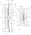
本例は、絶縁性接着剤を用いたインターポーザ10の接合方法及び、このインターポーザ10の接合方法を利用して作製した電子部品1に関する例である。この内容について、図1〜図6を用いて説明する。
本例のインターポーザ10の接合方法は、図1に示すごとく、シート状のチップ保持部材13に半導体チップ11を実装してなると共に該半導体チップ11から延設された接続端子であるインターポーザ側端子12を有するインターポーザ10を、シート状のベース部材21の表面にベース側端子22を設けたベース回路シート20に接合するものである。
このインターポーザ10の接合方法では、ベース回路シート20における少なくともベース側端子22の表面に電気的絶縁性を有する絶縁性接着材よりなる接着材配設層25を設ける接着剤塗付工程と、ベース側端子22とインターポーザ側端子12とが接着材配設層25を介設して対面するように、ベース回路シート20の表面にインターポーザ10を配置するインターポーザ配置工程と、相互に対面する一対のプレス型30を用いてベース回路シート20とインターポーザ10とを加圧する加圧プレス工程とを実施する。
ここで、ベース部材21及びチップ保持部材13の少なくとも一方は可塑性材料よりなる。ベース部材21及びチップ保持部材13のうち、可塑性材料よりなるものに隣接する上記一対のプレス型30の一方のプレス型(本例では、ダイ31。)は、インターポーザ側端子12あるいはベース側端子22の裏面に対面する加圧表面に、他方のプレス型(本例では、プレスアンビル32。図6参照。)に向けて突出する凸部310を設けてなる。
以下に、この内容について詳しく説明する。
一方、インターポーザ10側のプレス型32(以下、プレスアンビル32と記載する。)の加圧表面は、略平坦面としてある。また、熱可塑性材料よりなるベース部材21の突出変形を容易にすると共に、接着剤配設層25の絶縁性接着剤の流動性を高めるよう、本例のダイ31には、その加圧表面を加熱するための加熱ヒータ(図示略)を装備してある。
10 インターポーザ
11 半導体チップ(ICチップ)
12 インターポーザ側端子
13 チップ保持部材
20 ベース回路シート(アンテナシート)
21 ベース部材
22 ベース側端子
24 アンテナパターン
220 突出変形部
25 接着剤配設層
30 プレス型
31 ダイ
310 凸部
32 プレスアンビル
Claims (11)
- シート状のチップ保持部材の表面にインターポーザ側端子が形成されたインターポーザを、シート状のベース部材の表面にベース側端子が形成されたベース回路シートに接合するインターポーザの接合方法において、
上記ベース回路シートにおける少なくとも上記ベース側端子の表面に、電気的絶縁性を有する絶縁性接着材よりなる接着材配設層を設ける接着剤塗付工程と、
上記ベース側端子と上記インターポーザ側端子とが上記接着材配設層を介設して対面するように、上記ベース回路シートの表面に上記インターポーザを配置するインターポーザ配置工程と、
相互に対面する一対のプレス型を用いて上記ベース回路シートと上記インターポーザとを加圧する加圧プレス工程とを行い、
上記ベース部材及び上記チップ保持部材の少なくとも一方は可塑性材料よりなり、上記ベース部材及び上記チップ保持部材のうち、上記可塑性材料よりなるものに隣接する上記一対のプレス型の少なくとも一方のプレス型は、上記インターポーザ側端子あるいは上記ベース側端子の裏面に対面する加圧表面に、他方のプレス型に向けて突出する凸部を設けてなり、
上記接着剤塗付工程において上記接着剤配設層を形成する接着剤配設領域は、上記インターポーザ配置工程において上記インターポーザを配置するインターポーザ配置領域の全面を包含することを特徴とするインターポーザの接合方法。 - 請求項1において、上記絶縁性接着剤は、熱可塑性のものであり、上記凸部を設けた上記プレス型は、その上記加圧表面を加熱するための加熱ヒータを有してなることを特徴とするインターポーザの接合方法。
- 請求項2において、上記絶縁性接着剤は、湿気硬化型のものであることを特徴とするインターポーザの接合方法。
- 請求項1〜3のいずれか1項において、上記加圧プレス工程では、上記インターポーザ側端子と、上記ベース側端子との間に、超音波振動を作用することを特徴とするインターポーザの接合方法。
- 請求項1〜4のいずれか1項において、上記ベース回路シートは、上記ベース部材の表面に、導電パターンよりなる無線通信用のアンテナパターンを形成してなり、上記インターポーザは、上記チップ保持部材の表面にRF−ID用のICチップを実装してなることを特徴とするインターポーザの接合方法。
- インターポーザ側端子を備えたインターポーザをベース回路シートの表面に接合した電子部品であって、
上記ベース回路シートは、複数の突出変形部が形成されたベース側端子をシート状のベース部材の表面である端子形成面に有しており、
上記電子部品では、上記突出変形部が上記インターポーザ側端子に接触して該インターポーザ側端子と上記ベース側端子との間の電気的な導通が確保されていると共に、上記インターポーザ側端子と上記ベース側端子との間に形成された隙間に電気的な絶縁性を呈する絶縁性接着剤の接着剤配設層が形成されており、
上記接着剤配設層の接着剤配設領域は、上記インターポーザのインターポーザ配置領域の全面を包含することを特徴とする電子部品。 - インターポーザ側端子を備えたインターポーザを、ベース側端子を備えたベース回路シートの表面に接合した電子部品であって、
上記インターポーザの表面である端子形成面に形成された上記インターポーザ側端子には、複数の突出変形部が形成され、
上記電子部品では、上記突出変形部が上記ベース側端子に接触して該ベース側端子と上記インターポーザ側端子との間の電気的な導通が確保されていると共に、上記インターポーザ側端子と上記ベース側端子との間に形成された隙間に電気的な絶縁性を呈する絶縁性接着剤の接着剤配設層が形成されており、
上記接着剤配設層の接着剤配設領域は、上記インターポーザのインターポーザ配置領域の全面を包含することを特徴とする電子部品。 - 請求項6又は7において、上記突出変形部は、上記端子形成面の裏面側から上記端子形成面側に向かう突出変形により形成されていることを特徴とする電子部品。
- 請求項6〜8のいずれか1項において、上記ベース側端子又は上記インターポーザ側端子では、上記突出変形部が散点状に配置されていることを特徴とする電子部品。
- 請求項6〜9のいずれか1項において、上記インターポーザの外周側面と上記ベース回路シートの表面との間には、上記絶縁性接着剤よりなる法面が形成されていることを特徴とする電子部品。
- 請求項6〜10のいずれか1項に記載された電子部品であって、
請求項1〜5のいずれか1項のインターポーザの接合方法を用いて製造したことを特徴とする電子部品。
Priority Applications (3)
| Application Number | Priority Date | Filing Date | Title |
|---|---|---|---|
| JP2004329658A JP4628067B2 (ja) | 2004-11-12 | 2004-11-12 | インターポーザの接合方法、及び電子部品。 |
| PCT/JP2005/020654 WO2006051885A1 (ja) | 2004-11-12 | 2005-11-10 | インターポーザの接合方法及び、このインターポーザの接合方法を利用して作製した電子部品 |
| TW094139662A TW200628035A (en) | 2004-11-12 | 2005-11-11 | Interposer bonding method and electronic component manufactured using the same |
Applications Claiming Priority (1)
| Application Number | Priority Date | Filing Date | Title |
|---|---|---|---|
| JP2004329658A JP4628067B2 (ja) | 2004-11-12 | 2004-11-12 | インターポーザの接合方法、及び電子部品。 |
Publications (3)
| Publication Number | Publication Date |
|---|---|
| JP2006140359A JP2006140359A (ja) | 2006-06-01 |
| JP2006140359A5 JP2006140359A5 (ja) | 2008-09-11 |
| JP4628067B2 true JP4628067B2 (ja) | 2011-02-09 |
Family
ID=36336560
Family Applications (1)
| Application Number | Title | Priority Date | Filing Date |
|---|---|---|---|
| JP2004329658A Active JP4628067B2 (ja) | 2004-11-12 | 2004-11-12 | インターポーザの接合方法、及び電子部品。 |
Country Status (3)
| Country | Link |
|---|---|
| JP (1) | JP4628067B2 (ja) |
| TW (1) | TW200628035A (ja) |
| WO (1) | WO2006051885A1 (ja) |
Families Citing this family (5)
| Publication number | Priority date | Publication date | Assignee | Title |
|---|---|---|---|---|
| JP4855849B2 (ja) * | 2006-06-30 | 2012-01-18 | 富士通株式会社 | Rfidタグの製造方法、およびrfidタグ |
| JP5171405B2 (ja) * | 2008-06-05 | 2013-03-27 | 株式会社 ハリーズ | インターポーザ接合方法 |
| JP5437623B2 (ja) * | 2008-11-27 | 2014-03-12 | 株式会社 ハリーズ | Icタグ |
| US8584331B2 (en) * | 2011-09-14 | 2013-11-19 | Xerox Corporation | In situ flexible circuit embossing to form an electrical interconnect |
| JP5889718B2 (ja) * | 2012-05-30 | 2016-03-22 | アルプス電気株式会社 | 電子部品の実装構造体及び入力装置、ならびに、前記実装構造体の製造方法 |
Citations (4)
| Publication number | Priority date | Publication date | Assignee | Title |
|---|---|---|---|---|
| JPH04186697A (ja) * | 1990-11-19 | 1992-07-03 | Alps Electric Co Ltd | フレキシブルプリント基板の接続方法 |
| JPH09281520A (ja) * | 1996-04-10 | 1997-10-31 | Seiko Epson Corp | 回路基板の接続方法、液晶表示装置、電子機器 |
| JP2003069216A (ja) * | 2001-08-29 | 2003-03-07 | Toppan Forms Co Ltd | 導電接続部同士の接続方法 |
| JP2004111993A (ja) * | 2003-12-02 | 2004-04-08 | Hitachi Chem Co Ltd | 電極の接続方法およびこれに用いる接続部材 |
-
2004
- 2004-11-12 JP JP2004329658A patent/JP4628067B2/ja active Active
-
2005
- 2005-11-10 WO PCT/JP2005/020654 patent/WO2006051885A1/ja active Application Filing
- 2005-11-11 TW TW094139662A patent/TW200628035A/zh unknown
Patent Citations (4)
| Publication number | Priority date | Publication date | Assignee | Title |
|---|---|---|---|---|
| JPH04186697A (ja) * | 1990-11-19 | 1992-07-03 | Alps Electric Co Ltd | フレキシブルプリント基板の接続方法 |
| JPH09281520A (ja) * | 1996-04-10 | 1997-10-31 | Seiko Epson Corp | 回路基板の接続方法、液晶表示装置、電子機器 |
| JP2003069216A (ja) * | 2001-08-29 | 2003-03-07 | Toppan Forms Co Ltd | 導電接続部同士の接続方法 |
| JP2004111993A (ja) * | 2003-12-02 | 2004-04-08 | Hitachi Chem Co Ltd | 電極の接続方法およびこれに用いる接続部材 |
Also Published As
| Publication number | Publication date |
|---|---|
| TWI360379B (ja) | 2012-03-11 |
| JP2006140359A (ja) | 2006-06-01 |
| TW200628035A (en) | 2006-08-01 |
| WO2006051885A1 (ja) | 2006-05-18 |
Similar Documents
| Publication | Publication Date | Title |
|---|---|---|
| JP5036541B2 (ja) | 電子部品及び、この電子部品の製造方法 | |
| JP4855849B2 (ja) | Rfidタグの製造方法、およびrfidタグ | |
| US7960752B2 (en) | RFID tag | |
| KR20080003192A (ko) | Rfid 태그 제조 방법 및 rfid 태그 | |
| WO2007094167A1 (ja) | 回路基板および回路基板の製造方法 | |
| JP4091096B2 (ja) | インターポーザ接合装置 | |
| WO2006051885A1 (ja) | インターポーザの接合方法及び、このインターポーザの接合方法を利用して作製した電子部品 | |
| JP4754344B2 (ja) | Rfidタグ | |
| JP4860494B2 (ja) | 電子装置の製造方法 | |
| JP2000299411A (ja) | チップ実装体及びその製造方法 | |
| JP3891743B2 (ja) | 半導体部品実装済部品の製造方法、半導体部品実装済完成品の製造方法、及び半導体部品実装済完成品 | |
| JP3561117B2 (ja) | 無線モジュール及び無線カード | |
| JPH11103158A (ja) | プリント配線板へのフリップチップ実装方法および実装構造 | |
| JP5171405B2 (ja) | インターポーザ接合方法 | |
| JP2006140359A5 (ja) | ||
| CN101383022B (zh) | 电子部件 | |
| JP2613846B2 (ja) | 電極シート片付きチップ型電子部品 | |
| JP5029026B2 (ja) | 電子装置の製造方法 | |
| JP2004062634A (ja) | 非接触通信媒体の接合方法および非接触通信媒体 | |
| JP2002312749A (ja) | コンビ型icカードの製造方法 | |
| JP2003091709A (ja) | Icカード及びその製造方法 |
Legal Events
| Date | Code | Title | Description |
|---|---|---|---|
| A621 | Written request for application examination |
Free format text: JAPANESE INTERMEDIATE CODE: A621 Effective date: 20070802 |
|
| A521 | Request for written amendment filed |
Free format text: JAPANESE INTERMEDIATE CODE: A523 Effective date: 20080724 |
|
| RD02 | Notification of acceptance of power of attorney |
Free format text: JAPANESE INTERMEDIATE CODE: A7422 Effective date: 20090706 |
|
| A131 | Notification of reasons for refusal |
Free format text: JAPANESE INTERMEDIATE CODE: A131 Effective date: 20100727 |
|
| A521 | Request for written amendment filed |
Free format text: JAPANESE INTERMEDIATE CODE: A523 Effective date: 20100924 |
|
| TRDD | Decision of grant or rejection written | ||
| A01 | Written decision to grant a patent or to grant a registration (utility model) |
Free format text: JAPANESE INTERMEDIATE CODE: A01 Effective date: 20101102 |
|
| A01 | Written decision to grant a patent or to grant a registration (utility model) |
Free format text: JAPANESE INTERMEDIATE CODE: A01 |
|
| A61 | First payment of annual fees (during grant procedure) |
Free format text: JAPANESE INTERMEDIATE CODE: A61 Effective date: 20101109 |
|
| FPAY | Renewal fee payment (event date is renewal date of database) |
Free format text: PAYMENT UNTIL: 20131119 Year of fee payment: 3 |
|
| R150 | Certificate of patent or registration of utility model |
Ref document number: 4628067 Country of ref document: JP Free format text: JAPANESE INTERMEDIATE CODE: R150 Free format text: JAPANESE INTERMEDIATE CODE: R150 |
|
| R250 | Receipt of annual fees |
Free format text: JAPANESE INTERMEDIATE CODE: R250 |
|
| R250 | Receipt of annual fees |
Free format text: JAPANESE INTERMEDIATE CODE: R250 |
|
| R250 | Receipt of annual fees |
Free format text: JAPANESE INTERMEDIATE CODE: R250 |
|
| R250 | Receipt of annual fees |
Free format text: JAPANESE INTERMEDIATE CODE: R250 |
|
| S111 | Request for change of ownership or part of ownership |
Free format text: JAPANESE INTERMEDIATE CODE: R313113 |
|
| R350 | Written notification of registration of transfer |
Free format text: JAPANESE INTERMEDIATE CODE: R350 |
|
| R250 | Receipt of annual fees |
Free format text: JAPANESE INTERMEDIATE CODE: R250 |
|
| R250 | Receipt of annual fees |
Free format text: JAPANESE INTERMEDIATE CODE: R250 |
|
| R250 | Receipt of annual fees |
Free format text: JAPANESE INTERMEDIATE CODE: R250 |
|
| R250 | Receipt of annual fees |
Free format text: JAPANESE INTERMEDIATE CODE: R250 |
|
| R250 | Receipt of annual fees |
Free format text: JAPANESE INTERMEDIATE CODE: R250 |
|
| R250 | Receipt of annual fees |
Free format text: JAPANESE INTERMEDIATE CODE: R250 |
|
| R250 | Receipt of annual fees |
Free format text: JAPANESE INTERMEDIATE CODE: R250 |