JP4555642B2 - 信号処理回路 - Google Patents
信号処理回路 Download PDFInfo
- Publication number
- JP4555642B2 JP4555642B2 JP2004262231A JP2004262231A JP4555642B2 JP 4555642 B2 JP4555642 B2 JP 4555642B2 JP 2004262231 A JP2004262231 A JP 2004262231A JP 2004262231 A JP2004262231 A JP 2004262231A JP 4555642 B2 JP4555642 B2 JP 4555642B2
- Authority
- JP
- Japan
- Prior art keywords
- address
- signal
- color
- imaging
- read
- Prior art date
- Legal status (The legal status is an assumption and is not a legal conclusion. Google has not performed a legal analysis and makes no representation as to the accuracy of the status listed.)
- Expired - Fee Related
Links
Images


Description
また、本発明の信号処理回路において、前記メモリ制御部は、前記読み出しアドレスに追従して、前記書き込みアドレスを生成することを特徴とする。
Claims (4)
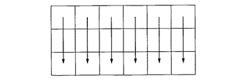
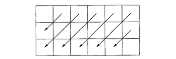
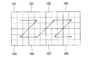
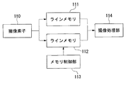
- 2次元に配列された画素から出力される画素信号のうち、複数の行に属する画素の画素信号を画素配列の順序とは異なる所定の順序で出力するように設計されたカラー撮像素子を用いて該カラー撮像素子の画素配列の順序でカラー撮像信号を処理するための信号処理回路であって、
前記カラー撮像素子から出力される画素信号を保持するラインメモリと、
該ラインメモリを制御するための書き込みアドレスと読み出しアドレスを生成するメモリ制御部を備え、
該メモリ制御部が生成する前記読み出しアドレスは、前記ラインメモリから読み出される前記画素信号の読み出し順序が、前記カラー撮像素子の画素配列の順序となるアドレスであり、
前記カラー撮像素子から最初に出力される行に属する画素の画素信号が前記ラインメモリから読み出されたあとの書き込みアドレスが、非連続のアドレスである
ことを特徴とする信号処理回路。 - 前記メモリ制御部は、前記読み出しアドレスに追従して、前記書き込みアドレスを生成することを特徴とする請求項1に記載の信号処理回路。
- 前記カラー撮像素子は、ベイヤ配列の色フィルタが貼付された受光面を具備していることを特徴とする請求項1に記載の信号処理回路。
- 前記メモリ制御部は、前記読み出しアドレスと前記書き込みアドレスとを異なる周波数で発生させることを特徴とする請求項1に記載の信号処理回路。
Priority Applications (1)
| Application Number | Priority Date | Filing Date | Title |
|---|---|---|---|
| JP2004262231A JP4555642B2 (ja) | 2004-09-09 | 2004-09-09 | 信号処理回路 |
Applications Claiming Priority (1)
| Application Number | Priority Date | Filing Date | Title |
|---|---|---|---|
| JP2004262231A JP4555642B2 (ja) | 2004-09-09 | 2004-09-09 | 信号処理回路 |
Publications (3)
| Publication Number | Publication Date |
|---|---|
| JP2006080853A JP2006080853A (ja) | 2006-03-23 |
| JP2006080853A5 JP2006080853A5 (ja) | 2009-11-12 |
| JP4555642B2 true JP4555642B2 (ja) | 2010-10-06 |
Family
ID=36159947
Family Applications (1)
| Application Number | Title | Priority Date | Filing Date |
|---|---|---|---|
| JP2004262231A Expired - Fee Related JP4555642B2 (ja) | 2004-09-09 | 2004-09-09 | 信号処理回路 |
Country Status (1)
| Country | Link |
|---|---|
| JP (1) | JP4555642B2 (ja) |
Families Citing this family (3)
| Publication number | Priority date | Publication date | Assignee | Title |
|---|---|---|---|---|
| JP4640831B2 (ja) * | 2006-03-30 | 2011-03-02 | シャープ株式会社 | データ処理装置、固体撮像装置、及び電子機器 |
| US7920191B2 (en) | 2006-12-08 | 2011-04-05 | Casio Computer Co., Ltd. | Image capturing apparatus in which pixel charge signals are divided and output in a different order than an arrangement of pixels on an image capturing element and then rearranged and stored in a same order as the arrangement of the pixels on the image capturing element, and method thereof |
| JP4983359B2 (ja) * | 2006-12-08 | 2012-07-25 | カシオ計算機株式会社 | 撮像装置及び撮像方法 |
Citations (6)
| Publication number | Priority date | Publication date | Assignee | Title |
|---|---|---|---|---|
| JPH0918763A (ja) * | 1995-06-30 | 1997-01-17 | Hitachi Ltd | 撮像装置および映像信号処理装置 |
| JPH10191185A (ja) * | 1996-12-20 | 1998-07-21 | Canon Inc | 画像信号処理装置 |
| JPH11234688A (ja) * | 1998-02-18 | 1999-08-27 | Sony Corp | 固体撮像装置の駆動方法及び固体撮像素子、並びにカメラ |
| JP2000059800A (ja) * | 1998-08-12 | 2000-02-25 | Mitsubishi Electric Corp | 画像信号処理回路 |
| JP2000244944A (ja) * | 1999-02-23 | 2000-09-08 | Aiphone Co Ltd | カラー映像伝送装置 |
| JP2001197509A (ja) * | 2000-01-14 | 2001-07-19 | Victor Co Of Japan Ltd | 撮像装置 |
-
2004
- 2004-09-09 JP JP2004262231A patent/JP4555642B2/ja not_active Expired - Fee Related
Patent Citations (6)
| Publication number | Priority date | Publication date | Assignee | Title |
|---|---|---|---|---|
| JPH0918763A (ja) * | 1995-06-30 | 1997-01-17 | Hitachi Ltd | 撮像装置および映像信号処理装置 |
| JPH10191185A (ja) * | 1996-12-20 | 1998-07-21 | Canon Inc | 画像信号処理装置 |
| JPH11234688A (ja) * | 1998-02-18 | 1999-08-27 | Sony Corp | 固体撮像装置の駆動方法及び固体撮像素子、並びにカメラ |
| JP2000059800A (ja) * | 1998-08-12 | 2000-02-25 | Mitsubishi Electric Corp | 画像信号処理回路 |
| JP2000244944A (ja) * | 1999-02-23 | 2000-09-08 | Aiphone Co Ltd | カラー映像伝送装置 |
| JP2001197509A (ja) * | 2000-01-14 | 2001-07-19 | Victor Co Of Japan Ltd | 撮像装置 |
Also Published As
| Publication number | Publication date |
|---|---|
| JP2006080853A (ja) | 2006-03-23 |
Similar Documents
| Publication | Publication Date | Title |
|---|---|---|
| JP2007228019A (ja) | 撮像装置 | |
| JP4379408B2 (ja) | 信号処理部および撮像装置 | |
| EP2451149A2 (en) | High-speed video camera | |
| JP5907687B2 (ja) | 撮像装置および信号転送装置 | |
| JP2008005048A (ja) | 撮像装置及び信号処理装置 | |
| JP2015053644A (ja) | 撮像装置 | |
| US9247168B2 (en) | Imaging device including focusing pixels | |
| JP4225241B2 (ja) | 画像表示装置 | |
| JP4606218B2 (ja) | 歪補正装置 | |
| JP4555642B2 (ja) | 信号処理回路 | |
| JP5972016B2 (ja) | 撮像装置 | |
| JP4697094B2 (ja) | 画像信号出力装置及びその制御方法 | |
| JP3700488B2 (ja) | 広角画像撮像装置 | |
| JP2002057943A (ja) | 撮像装置 | |
| JPH0564091A (ja) | ビデオカメラ | |
| JP4525388B2 (ja) | 撮像信号記録装置 | |
| JP4132264B2 (ja) | 画像信号処理回路 | |
| JP5225068B2 (ja) | 画像処理装置及び画像処理方法 | |
| US20230336871A1 (en) | Imaging element, imaging apparatus, operation method of imaging element, and program | |
| JP2007243819A (ja) | 画像処理装置 | |
| JP4424097B2 (ja) | 電子ズーム装置 | |
| JP4802482B2 (ja) | 画像処理装置及び画像処理方法 | |
| JP4271011B2 (ja) | 撮像処理装置 | |
| JP2015185936A (ja) | 撮像制御装置、撮像制御方法及びプログラム | |
| JP2005143031A (ja) | 静止画カラーカメラ装置 |
Legal Events
| Date | Code | Title | Description |
|---|---|---|---|
| A621 | Written request for application examination |
Free format text: JAPANESE INTERMEDIATE CODE: A621 Effective date: 20070710 |
|
| A521 | Request for written amendment filed |
Free format text: JAPANESE INTERMEDIATE CODE: A523 Effective date: 20090917 |
|
| A521 | Request for written amendment filed |
Free format text: JAPANESE INTERMEDIATE CODE: A821 Effective date: 20090918 |
|
| A977 | Report on retrieval |
Free format text: JAPANESE INTERMEDIATE CODE: A971007 Effective date: 20091203 |
|
| A131 | Notification of reasons for refusal |
Free format text: JAPANESE INTERMEDIATE CODE: A131 Effective date: 20091215 |
|
| A521 | Request for written amendment filed |
Free format text: JAPANESE INTERMEDIATE CODE: A523 Effective date: 20100205 |
|
| A521 | Request for written amendment filed |
Free format text: JAPANESE INTERMEDIATE CODE: A821 Effective date: 20100208 |
|
| TRDD | Decision of grant or rejection written | ||
| A01 | Written decision to grant a patent or to grant a registration (utility model) |
Free format text: JAPANESE INTERMEDIATE CODE: A01 Effective date: 20100706 |
|
| A01 | Written decision to grant a patent or to grant a registration (utility model) |
Free format text: JAPANESE INTERMEDIATE CODE: A01 |
|
| A61 | First payment of annual fees (during grant procedure) |
Free format text: JAPANESE INTERMEDIATE CODE: A61 Effective date: 20100716 |
|
| FPAY | Renewal fee payment (event date is renewal date of database) |
Free format text: PAYMENT UNTIL: 20130723 Year of fee payment: 3 |
|
| R151 | Written notification of patent or utility model registration |
Ref document number: 4555642 Country of ref document: JP Free format text: JAPANESE INTERMEDIATE CODE: R151 |
|
| FPAY | Renewal fee payment (event date is renewal date of database) |
Free format text: PAYMENT UNTIL: 20130723 Year of fee payment: 3 |
|
| S531 | Written request for registration of change of domicile |
Free format text: JAPANESE INTERMEDIATE CODE: R313531 |
|
| R350 | Written notification of registration of transfer |
Free format text: JAPANESE INTERMEDIATE CODE: R350 |
|
| LAPS | Cancellation because of no payment of annual fees |