JP4324362B2 - Low defect density ideal oxygen precipitated silicon - Google Patents
Low defect density ideal oxygen precipitated silicon Download PDFInfo
- Publication number
- JP4324362B2 JP4324362B2 JP2002303260A JP2002303260A JP4324362B2 JP 4324362 B2 JP4324362 B2 JP 4324362B2 JP 2002303260 A JP2002303260 A JP 2002303260A JP 2002303260 A JP2002303260 A JP 2002303260A JP 4324362 B2 JP4324362 B2 JP 4324362B2
- Authority
- JP
- Japan
- Prior art keywords
- wafer
- concentration
- region
- vacancies
- temperature
- Prior art date
- Legal status (The legal status is an assumption and is not a legal conclusion. Google has not performed a legal analysis and makes no representation as to the accuracy of the status listed.)
- Expired - Lifetime
Links
Images


Classifications
-
- C—CHEMISTRY; METALLURGY
- C30—CRYSTAL GROWTH
- C30B—SINGLE-CRYSTAL GROWTH; UNIDIRECTIONAL SOLIDIFICATION OF EUTECTIC MATERIAL OR UNIDIRECTIONAL DEMIXING OF EUTECTOID MATERIAL; REFINING BY ZONE-MELTING OF MATERIAL; PRODUCTION OF A HOMOGENEOUS POLYCRYSTALLINE MATERIAL WITH DEFINED STRUCTURE; SINGLE CRYSTALS OR HOMOGENEOUS POLYCRYSTALLINE MATERIAL WITH DEFINED STRUCTURE; AFTER-TREATMENT OF SINGLE CRYSTALS OR A HOMOGENEOUS POLYCRYSTALLINE MATERIAL WITH DEFINED STRUCTURE; APPARATUS THEREFOR
- C30B15/00—Single-crystal growth by pulling from a melt, e.g. Czochralski method
-
- H—ELECTRICITY
- H01—ELECTRIC ELEMENTS
- H01L—SEMICONDUCTOR DEVICES NOT COVERED BY CLASS H10
- H01L21/00—Processes or apparatus adapted for the manufacture or treatment of semiconductor or solid state devices or of parts thereof
- H01L21/02—Manufacture or treatment of semiconductor devices or of parts thereof
- H01L21/04—Manufacture or treatment of semiconductor devices or of parts thereof the devices having at least one potential-jump barrier or surface barrier, e.g. PN junction, depletion layer or carrier concentration layer
- H01L21/18—Manufacture or treatment of semiconductor devices or of parts thereof the devices having at least one potential-jump barrier or surface barrier, e.g. PN junction, depletion layer or carrier concentration layer the devices having semiconductor bodies comprising elements of Group IV of the Periodic System or AIIIBV compounds with or without impurities, e.g. doping materials
- H01L21/30—Treatment of semiconductor bodies using processes or apparatus not provided for in groups H01L21/20 - H01L21/26
- H01L21/322—Treatment of semiconductor bodies using processes or apparatus not provided for in groups H01L21/20 - H01L21/26 to modify their internal properties, e.g. to produce internal imperfections
- H01L21/3221—Treatment of semiconductor bodies using processes or apparatus not provided for in groups H01L21/20 - H01L21/26 to modify their internal properties, e.g. to produce internal imperfections of silicon bodies, e.g. for gettering
- H01L21/3225—Thermally inducing defects using oxygen present in the silicon body for intrinsic gettering
-
- C—CHEMISTRY; METALLURGY
- C30—CRYSTAL GROWTH
- C30B—SINGLE-CRYSTAL GROWTH; UNIDIRECTIONAL SOLIDIFICATION OF EUTECTIC MATERIAL OR UNIDIRECTIONAL DEMIXING OF EUTECTOID MATERIAL; REFINING BY ZONE-MELTING OF MATERIAL; PRODUCTION OF A HOMOGENEOUS POLYCRYSTALLINE MATERIAL WITH DEFINED STRUCTURE; SINGLE CRYSTALS OR HOMOGENEOUS POLYCRYSTALLINE MATERIAL WITH DEFINED STRUCTURE; AFTER-TREATMENT OF SINGLE CRYSTALS OR A HOMOGENEOUS POLYCRYSTALLINE MATERIAL WITH DEFINED STRUCTURE; APPARATUS THEREFOR
- C30B15/00—Single-crystal growth by pulling from a melt, e.g. Czochralski method
- C30B15/20—Controlling or regulating
- C30B15/203—Controlling or regulating the relationship of pull rate (v) to axial thermal gradient (G)
-
- C—CHEMISTRY; METALLURGY
- C30—CRYSTAL GROWTH
- C30B—SINGLE-CRYSTAL GROWTH; UNIDIRECTIONAL SOLIDIFICATION OF EUTECTIC MATERIAL OR UNIDIRECTIONAL DEMIXING OF EUTECTOID MATERIAL; REFINING BY ZONE-MELTING OF MATERIAL; PRODUCTION OF A HOMOGENEOUS POLYCRYSTALLINE MATERIAL WITH DEFINED STRUCTURE; SINGLE CRYSTALS OR HOMOGENEOUS POLYCRYSTALLINE MATERIAL WITH DEFINED STRUCTURE; AFTER-TREATMENT OF SINGLE CRYSTALS OR A HOMOGENEOUS POLYCRYSTALLINE MATERIAL WITH DEFINED STRUCTURE; APPARATUS THEREFOR
- C30B15/00—Single-crystal growth by pulling from a melt, e.g. Czochralski method
- C30B15/20—Controlling or regulating
- C30B15/206—Controlling or regulating the thermal history of growing the ingot
-
- C—CHEMISTRY; METALLURGY
- C30—CRYSTAL GROWTH
- C30B—SINGLE-CRYSTAL GROWTH; UNIDIRECTIONAL SOLIDIFICATION OF EUTECTIC MATERIAL OR UNIDIRECTIONAL DEMIXING OF EUTECTOID MATERIAL; REFINING BY ZONE-MELTING OF MATERIAL; PRODUCTION OF A HOMOGENEOUS POLYCRYSTALLINE MATERIAL WITH DEFINED STRUCTURE; SINGLE CRYSTALS OR HOMOGENEOUS POLYCRYSTALLINE MATERIAL WITH DEFINED STRUCTURE; AFTER-TREATMENT OF SINGLE CRYSTALS OR A HOMOGENEOUS POLYCRYSTALLINE MATERIAL WITH DEFINED STRUCTURE; APPARATUS THEREFOR
- C30B29/00—Single crystals or homogeneous polycrystalline material with defined structure characterised by the material or by their shape
- C30B29/02—Elements
- C30B29/06—Silicon
-
- C—CHEMISTRY; METALLURGY
- C30—CRYSTAL GROWTH
- C30B—SINGLE-CRYSTAL GROWTH; UNIDIRECTIONAL SOLIDIFICATION OF EUTECTIC MATERIAL OR UNIDIRECTIONAL DEMIXING OF EUTECTOID MATERIAL; REFINING BY ZONE-MELTING OF MATERIAL; PRODUCTION OF A HOMOGENEOUS POLYCRYSTALLINE MATERIAL WITH DEFINED STRUCTURE; SINGLE CRYSTALS OR HOMOGENEOUS POLYCRYSTALLINE MATERIAL WITH DEFINED STRUCTURE; AFTER-TREATMENT OF SINGLE CRYSTALS OR A HOMOGENEOUS POLYCRYSTALLINE MATERIAL WITH DEFINED STRUCTURE; APPARATUS THEREFOR
- C30B33/00—After-treatment of single crystals or homogeneous polycrystalline material with defined structure
- C30B33/02—Heat treatment
-
- Y—GENERAL TAGGING OF NEW TECHNOLOGICAL DEVELOPMENTS; GENERAL TAGGING OF CROSS-SECTIONAL TECHNOLOGIES SPANNING OVER SEVERAL SECTIONS OF THE IPC; TECHNICAL SUBJECTS COVERED BY FORMER USPC CROSS-REFERENCE ART COLLECTIONS [XRACs] AND DIGESTS
- Y10—TECHNICAL SUBJECTS COVERED BY FORMER USPC
- Y10T—TECHNICAL SUBJECTS COVERED BY FORMER US CLASSIFICATION
- Y10T428/00—Stock material or miscellaneous articles
- Y10T428/21—Circular sheet or circular blank
-
- Y—GENERAL TAGGING OF NEW TECHNOLOGICAL DEVELOPMENTS; GENERAL TAGGING OF CROSS-SECTIONAL TECHNOLOGIES SPANNING OVER SEVERAL SECTIONS OF THE IPC; TECHNICAL SUBJECTS COVERED BY FORMER USPC CROSS-REFERENCE ART COLLECTIONS [XRACs] AND DIGESTS
- Y10—TECHNICAL SUBJECTS COVERED BY FORMER USPC
- Y10T—TECHNICAL SUBJECTS COVERED BY FORMER US CLASSIFICATION
- Y10T428/00—Stock material or miscellaneous articles
- Y10T428/249921—Web or sheet containing structurally defined element or component
- Y10T428/249953—Composite having voids in a component [e.g., porous, cellular, etc.]
- Y10T428/249967—Inorganic matrix in void-containing component
- Y10T428/249969—Of silicon-containing material [e.g., glass, etc.]
Description
【0001】
【発明の属する技術分野】
本発明は一般に、電子部品の製造に使用される、半導体材料基板、特にシリコンウエハに関する。本発明は特に、本質的にどの任意の電子デバイス製造プロセスの熱処理サイクルの間にも、理想的な不均一深さ分布の酸素析出物を形成し、および、凝集真性点欠陥を実質的に有さない軸対称領域を付加的に有する、シリコンウエハならびにその製造方法に関する。
【0002】
【従来の技術】
半導体電子部品のほとんどの製造方法の出発物質である単結晶シリコンは一般に、単一種結晶を溶融シリコンに浸漬し、次に遅い引き上げ(extraction)によって成長させる、いわゆるチョクラルスキー法によって製造される。溶融シリコンは石英ルツボに装填されるので、種々の不純物、主に酸素、によって汚染される。溶融塊の温度におけるシリコン中の酸素の溶解度および凝固シリコンにおける酸素の事実上の偏析係数によって測定されるある濃度に酸素が到達するまで、シリコン溶融塊の温度において、酸素が結晶格子に入る。そのような濃度は、電子デバイス製造プロセスに一般的な温度における固体シリコン中の酸素の溶解度より大きい。結晶が溶融塊から成長し冷却し、従ってその中の酸素の溶解度が急速に減少し、それによって、得られるスライスまたはウエハにおいて酸素が過飽和濃度において存在する。
【0003】
電子デバイスの製造に一般に使用される熱処理サイクルは、酸素で過飽和されたシリコンウエハにおいて、酸素の析出を生じうる。ウエハにおける析出の位置に依存して、析出は有害にも有益にもなりうる。ウエハの活性デバイス領域に位置する酸素析出は、デバイスの操作を害することがある。しかし、バルクに存在する酸素析出は、ウエハに接触する望ましくない金属性不純物を捕捉することができる。ウエハのバルクに位置する酸素析出を、金属を捕捉するために使用することは一般に、内部ゲッタリングまたはイントリンシック・ゲッタリング(IG)と称される。
【0004】
歴史的に、電子デバイス製造プロセスは、ウエハの表面近くに酸素析出物を有さない帯域(zone)または領域(region)(一般に、「デニューデッドゾーン」または「無析出帯域」と称される。)を有し、ウエハの残り部分、即ちウエハバルクは、IGのために充分な数の酸素析出物を有するシリコンを製造するように設計された一連の段階を包含する。デニューデッドゾーンは、例えば、(a)高温(>1100℃)における不活性雰囲気中での少なくとも約4時間の酸素外部拡散熱処理、(b)低温(600℃〜750℃)における酸素析出核形成、および(c)高温(1000℃〜1150℃)における酸素(SiO2)析出物の成長、のような高温−低温−高温の熱シーケンスにおいて、形成することができる。例えば、F. Shimura, Semiconductor Silicon Crystal Technology, Academic Press,Inc., San Diego Calofornia (1989), p361〜367、およびそこに引用されている文献を参照。
【0005】
しかし、最近では、DRAM製造方法のような先進の電子デバイス製造方法が、高温プロセス段階の使用を最少限にするようになってきている。これらのプロセスには、高温プロセス段階をまだ使用して、デニューデッドゾーンおよび充分な密度のバルク析出を形成しているものもあるが、そのような材料に対する許容度は非常に低く、商業的に存続できる製品になりえない。他の現在の高度に先進の電子デバイス製造方法は、外部拡散段階を全く含まない。活性デバイス領域における酸素析出に付随する問題の故に、これらの電子デバイス製造者は、工程条件下にウエハのどの位置にも酸素析出物を形成しないシリコンウエハを使用しなければならない。その結果、IGの可能性が全て失われる。
【0006】
【発明が解決しようとする課題】
従って、本発明の目的は、本質的にどの電子デバイス製造プロセスの熱処理サイクルの間にも、理想的な不均一深さ分布の酸素析出物を形成する単結晶シリコンウエハの提供;充分な深さのデニューデッドゾーン、およびウエハバルクにおける充分な密度の酸素析出物を、最適におよび再現的に形成するウエハの提供;デニューデッドゾーンの形成、およびウエハバルクにおける酸素析出物の形成が、ウエハのこれらの領域における酸素濃度の差異に依存しないウエハの提供;デニューデッドゾーンの形成が、酸素の外部拡散に依存しない方法の提供;得られるデニューデッドゾーンの厚みが、IC製造工程シーケンスの細部に本質的に依存しないウエハの提供;デニューデッドゾーンの形成、およびウエハバルクにおける酸素析出物の形成が、それからシリコンウエハがスライスされるチョクラルスキー成長単結晶シリコンインゴットの、熱履歴および酸素濃度によって影響を受けないウエハの提供;および、結晶格子空孔またはシリコン自己格子間原子の凝集から生じる欠陥を実質的に有さない、実質的な半径幅の軸対称領域を付加的に有するウエハの提供;である。
【0007】
【課題を解決するための手段】
従って、簡単に言えば、本発明は、一方がウエハの前表面であり他方がウエハの後表面であるほぼ平行な2つの主表面;前表面と後表面の間の中央面;前表面と後表面を接合する周囲縁;前表面から中央面の方向に測定される少なくとも約10マイクロメートルの距離D1と前表面の間のウエハの領域を有して成る表面層;および、中央面と第一領域の間のウエハの第二領域を有して成るバルク層;を有する単結晶シリコンウエハに関する。特に、該ウエハは、結晶格子空孔の不均一分布を有し、バルク層における空孔の濃度は、表面層における空孔の濃度より大きく、空孔は、空孔のピーク密度が中央面かまたはその付近に存在し、その濃度がピーク密度の位置からウエハの前表面の方向に一般に減少する濃度輪郭を有する。1つの実施態様においては、空孔が優勢な真性点欠陥であり、凝集真性点欠陥を実質的に有さない第一軸対称領域を、ウエハが付加的に有し、該第一軸対称領域は、中心軸を有して成るかまたは少なくとも約15mmの幅を有する。他の実施態様においては、凝集真性点欠陥を実質的に有さない軸対称領域を、ウエハが付加的に有し、該軸対称領域は、ウエハの周囲縁から半径方向に内向きに延在し、周囲縁から中心軸に向かって半径方向に測定される幅を有し、該幅はウエハの半径の長さの少なくとも約40%である。
【0008】
本発明は、一方がウエハの前表面であり他方がウエハの後表面であるほぼ平行な2つの主表面;前表面と後表面の間の中央面;前表面と後表面を接合する周囲縁;前表面の約15マイクロメートル以下の距離D2内のウエハの領域を有して成る前表面層;および、中央面と前表面層の間のウエハの領域を有して成るバルク層;を有する単結晶シリコンウエハにも関する。特に、800℃において4時間、次に1000℃において16時間でウエハをアニールすることから本質的に成る酸素析出熱処理にウエハを曝露したときに、バルク層における析出物のピーク密度が中央面かまたはその付近に存在し、バルク層における析出物の濃度が前表面層の方向に一般に減少する濃度輪郭を有する酸素析出物をウエハが含有するような、実質的に均一な酸素濃度および結晶格子空孔の濃度を、バルク層が有する。1つの実施態様においては、空孔が優勢な真性点欠陥であり、凝集真性点欠陥を実質的に有さない第一軸対称領域を、ウエハが付加的に有し、該第一軸対称領域は、中心軸を有して成るかまたは少なくとも約15mmの幅を有する。他の態様においては、凝集真性点欠陥を実質的に有さない軸対称領域を、ウエハが付加的に有して成り、該軸対称領域は、ウエハの周囲縁から半径方向に内向きに延在し、周囲縁から中心軸に向かって半径方向に測定される幅を有し、該幅はウエハの半径の長さの少なくとも約40%である。
【0009】
本発明は、一方がウエハの前表面であり他方がウエハの後表面であるほぼ平行な2つの主表面;前表面と後表面の間の中央面;および、前表面と後表面を接合する周囲縁;を有する単結晶シリコンウエハにも関する。格子間酸素を含有し、および前表面から、前表面から中央面に向かって測定される少なくとも10マイクロメートルの距離D1までの、ウエハの領域を有して成るデニューデッドゾーンを有して成ることを、該ウエハは特徴とする。該ウエハは、D1の2分の1に相当する距離におけるデニューデッドゾーンにおける格子間酸素の濃度が、デニューデッドゾーンの格子間酸素の最大濃度の少なくとも約75%であることも特徴とする。1つの実施態様において、空孔が優勢真性点欠陥であり、凝集真性点欠陥を実質的に有さない第一軸対称領域を有して成ることも該ウエハは特徴とし、該第一軸対称領域は、中心軸を有して成るかまたは少なくとも約15mmの幅を有する。他の実施態様においては、凝集真性点欠陥を実質的に有さない軸対称領域を、ウエハが有して成り、該軸対称領域は、ウエハの周囲縁から半径方向に内向きに延在し、および周囲縁から中心軸に向かって半径方向に測定される幅を有し、該幅はウエハの半径の長さの少なくとも約40%である。
【0010】
本発明はさらに、一方がウエハの前表面であり他方がウエハの後表面であるほぼ平行な2つの主表面;前表面と後表面の間の中央面;および、前表面と後表面を接合する周囲縁;前表面の約15マイクロメートル以下の距離D2内のウエハの領域から成る前表面層;および、中央面と前表面層の間のウエハの領域を有して成るバルク層;を有する単結晶シリコンウエハにも関する。特に、800℃において4時間、次に1000℃において16時間でウエハをアニールすることから本質的に成る酸素析出熱処理にウエハを曝露したときに、バルク層における析出物のピーク密度が中央面かまたはその付近に存在し、バルク層における析出物の濃度が前表面層の方向に一般に減少する濃度輪郭を有する酸素析出物をウエハが含有するような、実質的に均一な酸素濃度および結晶格子空孔の濃度を、バルク層が有する。
【0011】
本発明はさらに、後の熱加工段階におけるウエハにおける酸素の析出挙動に影響を与えるために、Cz単結晶シリコンウエハを熱処理する方法にも関する。ウエハは、前表面;後表面;前表面と後表面の間の中央面;前表面における空孔シンク(vacancy sink);前表面と、前表面から中央面に向かって測定される距離D1の間の、ウエハの領域を有して成る前表面層;中央面と、ウエハの前表面から測定される距離D1の間の、ウエハの領域を有して成るバルク層;および、凝集真性点欠陥を実質的に有さない軸対称領域;を有する。該方法においては、ウエハを熱処理して、ウエハ中に結晶格子空孔を形成する。次に、熱処理されたウエハにおける空孔の濃度を、熱処理されたウエハの冷却速度を調節することによって減少させて、ピーク密度が中央面かまたはその付近に存在し、その濃度がウエハの前表面の方向に一般に減少する空孔濃度輪郭を有するウエハを形成する。前表面層およびバルク層における空孔の濃度の差異は、750℃より高い温度におけるウエハの熱処理が、前表面層におけるデニューデッドゾーンの形成およびバルク帯域における酸素クラスターまたは析出物の形成に導くような差異であり、酸素クラスターまたは析出物の濃度はバルク層における空孔の濃度に主として依存する。
【0012】
本発明の他の目的および特徴は、一部は明らかであり、一部は下記に記載される。
【0013】
本発明により、理想的な析出ウエハが見いだされた。このウエハは、本質的には、任意の電子デバイス製造工程の途中で、IG目的のために充分な深さのデニューデッドゾーンと、充分な密度の酸素析出物を含むウエハバルクとを形成する。この理想的な析出ウエハは、好都合なことに、半導体シリコン製造業で一般的に使用されている用具を使用して短時間で調製することができる。このような処理により、電子デバイス製造工程の途中で酸素が析出する様式を決定するか、または「印刷」する「テンプレート」がシリコンに形成される。
【0014】
本発明の理想的な析出ウエハの出発材料は、従来のチョクラルスキー(Czochralski)結晶成長法に従って成長させた単結晶インゴットからスライスされた単結晶ウエハである。そのような方法は、標準的なシリコンスライス技術、ラップ処理(lapping)技術、エッチング技術および研磨技術と同様に、例えば、F.Shimura、Semiconductor Silicon Crystal Technology、Academic Press(1989)、およびSilicon Chemical Etching (J.Grabmaier編) Springer-Verlag、New York(1982)に開示されている(これらは参考として本明細書中に援用される)。チョクラルスキー成長シリコンは、典型的には、約5×10¹⁷原子/cm3〜約9×1017原子/cm3(ASTM規格F-121-83)の範囲内の酸素濃度を有する。ウエハの酸素析出挙動は、理想的な析出ウエハ中の酸素濃度と本質的には連携していないので、出発ウエハの酸素濃度は、チョクラルスキープロセスによって到達可能な範囲内の任意の濃度またはその範囲外の任意の濃度でさえあり得る。
【0015】
シリコンの融点(約1410℃)温度から約750℃〜約350℃の範囲への単結晶シリコンインゴットの冷却速度に依存して、酸素析出物の核形成中心が、ウエハがスライスされる単結晶シリコンインゴットに形成し得る。しかし、出発材料におけるこのような核形成中心の有無は、これらの中心が約1300℃を超えない温度でシリコンを熱処理することによって溶解し得る場合には本発明にとって重要でない。約800℃の温度で約4時間のシリコンのアニーリング処理などのいくつかの熱処理は、このような中心が約1150℃を超えない温度で溶解し得ないように、これらの中心を安定化させることができる。酸素析出物の検出限界は、現在、約5×10⁶析出物/cm3である。酸素析出の核形成中心の存在(または、密度)は、現在の利用可能な技術を使用して直接的に測定することができない。しかし、様々な技術を使用して、その存在を間接的に検出することができる。前記のように、シリコン中の以前から存在する酸素析出物核形成中心を安定化させることができ、そして、析出物は、シリコンを酸素析出熱処理に供することによってこのような部位で成長させることができる。従って、このような核形成中心の存在は、例えば、800℃の温度で4時間、次いで1000℃の温度で16時間のウエハのアニーリング処理などの酸素析出熱処理の後で間接的に測定することができる。
【0016】
置換炭素は、単結晶シリコン中の不純物として存在する場合、酸素析出核形成中心を形成させる触媒能を有する。従って、このような理由および他の理由のために、単結晶シリコンの出発材料は、低濃度の炭素を有することが好ましい。すなわち、単結晶シリコンは、約5×10¹⁶原子/cm3未満であり、好ましくは約1×1016原子/cm3未満であり、より好ましくは約5×1015原子/cm3未満の炭素濃度を有する。
【0017】
次に、図1を参照すると、本発明の理想的な析出ウエハの出発材料である単結晶シリコンウエハ1は、前表面3、後表面5、および前表面と後表面との間の仮想的な中央面7を有する。本明細書における用語「前(表面)」および「後(表面)」は、ウエハの2つのほぼ平らな主表面を区別するために使用される;ウエハの前表面は、その用語が本明細書中で使用される場合、必ずしも、電子デバイスが続いて組み立てられる表面である必要はなく、ウエハの後表面は、その用語が本明細書中で使用される場合、必ずしも、電子デバイスが組み立てられる表面の反対側のウエハの主表面である必要はない。さらに、シリコンウエハは、典型的には、ある程度の全体的な厚みの変動(TTV)、反り(warp)および湾曲(bow)を有するので、前表面の任意の点と後表面の任意の点との中間点は、正確には、1つの平面に含まれ得ない;しかし、実際問題として、TTV、反りおよび湾曲は非常にわずかであるので、近い近似では、そのような中間点は、前表面と後表面との間のほぼ等しい距離にある仮想的な中央面に含まれると言うことができる。
【0018】
本発明のプロセスの第1の実施形態において、ウエハ1は、ウエハ1を包み込む表面酸化物層9を成長させるために、工程S1において酸素含有雰囲気中で熱処理される。一般に、酸化物層は、シリコン表面に生成する自然の酸化物層(約15オングストローム)よりも大きな厚さを有する;この酸化物層は、好ましくは、少なくとも約20オングストロームの厚さを有し、いくつかの実施形態においては、少なくとも約25オングストロームの厚さを有するか、または少なくとも約30オングストロームの厚ささえ有する。しかし、今日までに得られた実験的証拠により、約30オングストロームを超える厚さの酸化物層は、所望の効果を妨害しないが、さらなる利点はほとんど得られないことが示唆される。
【0019】
工程S2において、ウエハは、ウエハを高温に加熱して、ウエハ1において結晶格子の空孔(空格子点)13を形成させ、それによりその数密度を増大させる熱処理工程に供される。この熱処理工程は、好ましくは、ウエハを目標温度に迅速に加熱し、その温度で比較的短時間アニーリング処理する急速熱アニーリング装置で行われる。一般に、ウエハは、1150℃を超える温度に、好ましくは、少なくとも1175℃に、より好ましくは少なくとも約1200℃に、最も好ましくは、約1200℃と1275℃との間の温度に曝される。
【0020】
本発明の上記の第1の実施形態において、急速熱アニーリング工程は、窒化物形成性の雰囲気、すなわち、窒素ガス(N2)を含有する雰囲気、または暴露されたシリコン表面を窒化物にし得る窒素含有化合物ガス(アンモニアなど)を含有する雰囲気のもとで行われる。従って、そのような雰囲気は、全体が窒素ガスまたは窒素化合物ガスから構成され得る。あるいは、そのような雰囲気は、アルゴンなどの窒化物非形成性のガスをさらに含むことができる。ウエハ全体の空孔濃度(空格子点濃度)の増大が、直ちではないとしても、アニーリング温度に到達したときにほぼ達成される。ウエハは、一般に、この温度で、少なくとも1秒間、典型的には少なくとも数秒間(例えば、少なくとも3秒間)、好ましくは数十秒間(例えば、20秒間、30秒間、40秒間または50秒間)、およびウエハの所望の特性に依存して、約60秒(これは市販の急速熱アニーリング装置のほぼ限界である)までの範囲であり得る期間保持される。得られるウエハは、このウエハにおいて比較的均一な空孔濃度(数密度)特性を有する。
【0021】
今日までに得られた実験的証拠に基づいて、急速熱アニーリング工程が行われる雰囲気は、好ましくは、酸素、水蒸気および他の酸化性ガスの比較的小さな分圧を有するに過ぎない;すなわち、その雰囲気は、酸化性ガスが全く存在しないか、またはそのようなガスの分圧を全く有せず、空孔濃度の成長を抑制するシリコン自己格子間原子の充分量を注入するのに不充分である。酸化性ガスの下限濃度は正確には決定されていないが、0.01気圧(atm)すなわち10,000部/百万原子(ppma)の酸素分圧に関して、空孔濃度の増大および効果が認められないことが明らかにされている。従って、雰囲気は、酸素および他の酸化性ガスの分圧が0.01atm(10,000ppma)未満であることが好ましい;より好ましくは、雰囲気中におけるこれらのガスの分圧は約0.002atm(2,000ppma)以下であり、より好ましくは約0.005atm(5,000ppma)以下であり、最も好ましくは約0.001atm(1,000ppma)以下である。
【0022】
結晶格子の空孔が生成することに加えて、急速熱アニーリング工程は、シリコンの出発材料中に存在する安定化されていない任意の酸素析出物核形成中心を溶解する。このような核形成中心は、例えば、ウエハがスライスされる単結晶シリコンインゴットの成長途中で形成され得るか、またはウエハまたはウエハがスライスされるインゴットの以前の熱履歴におけるいくつかの他の事象の結果として形成され得る。従って、出発材料におけるこのような核形成中心の有無は、これらの中心が、急速熱アニリーング工程の最中で溶解し得る場合には重要ではない。
【0023】
急速熱アニーリング処理は、ウエハが高出力光源の列によって個々に加熱される多数の市販の急速熱アニーリング(「RTA」)処理炉のいずれかで行うことができる。RTA炉は、シリコンウエハを急速に加熱することができる。例えば、RTA炉は、ウエハを室温から1200℃まで数秒間で加熱することができる。そのような市販のRTA炉の1つは、AG Associates(Mountain View、CA)から入手できるモデル610炉である。
【0024】
真性点欠陥(空孔およびシリコン自己格子間原子)は、温度に依存する拡散速度で単結晶シリコン中を拡散し得る。従って、真性点欠陥の濃度特性は、温度を関数とする真性点欠陥の拡散係数および再結合速度の関数である。例えば、真性点欠陥は、急速熱アニーリング工程においてウエハがアニーリング処理される温度の近傍温度で比較的移動し得るが、700℃もの温度では、本質的に、任意の商業的に実用的な時間で移動し得ない。これまでに得られた実験的証拠により、空孔の有効拡散速度は、約700℃未満の温度で、そしておそらくは、800℃または900℃あるいは1000℃さえもの温度ほどに高い温度でかなり遅いことが示唆される。空孔は、任意の商業的に実用的な時間で移動しないと見なすことができる。
【0025】
工程S2が終了したとき、ウエハは、結晶格子の空孔が単結晶シリコン内で比較的移動し得る温度範囲を通過するように(または該温度範囲まで)工程S3において急冷される。ウエハの温度がこの範囲の温度を通過して下がるとき、空孔は、酸化物層9に拡散して消滅し、従って、ウエハがこの範囲内の温度で保持された時間の長さに依存する変化度を伴って空孔の濃度特性の変化をもたらす。ウエハがこの範囲内のこの温度で無限の時間保持されたならば、空孔濃度は、再度、ウエハバルク11の全体に実質的に均一になり、その濃度は、熱処理工程の終了直後における結晶格子の空孔濃度よりも実質的に少ない平衡値である。しかし、ウエハを急冷することによって、結晶格子の空孔の不均一な分布が達成され得るが、最大の空孔濃度は、中央面7またはその近くに存在し、空孔濃度は、ウエハの前表面3および後表面5の方向で減少する。一般に、この範囲の温度内での平均冷却速度は、少なくとも約5℃/秒であり、好ましくは少なくとも約20℃/秒である。デニューデッドゾーンの所望の深さに依存して、平均冷却速度は、好ましくは少なくとも50℃/秒であり、さらにより好ましくは少なくとも100℃/秒であるが、いくつかの適用に関しては、現在、約100℃/秒〜約200℃/秒の範囲の冷却速度が好ましい。ウエハが、結晶格子の空孔が単結晶シリコン内で比較的移動し得る温度範囲の外側の温度に冷却されると、冷却速度は、ウエハの析出特性に大きな影響を与えないようであり、従って、冷却速度は、きわどいほど臨界的ではないようである。便宜上、冷却工程は、加熱工程が行われる同じ雰囲気中で行うことができる。
【0026】
工程S4において、ウエハは、酸素析出熱処理に供される。例えば、ウエハは、800℃の温度で4時間、次いで1000℃の温度で16時間アニーリング処理することができる。あるいは、ウエハは、好ましくは、電子デバイス製造プロセスの最初の工程のように、約800℃の温度の炉に入れられる。この温度の炉に入れられたときに、前記の急速熱アニーリング処理されたウエハは、酸素析出に関して異なった挙動をする異なる帯域を有する。高い空孔領域(ウエハバルク)において、酸素は、ウエハが炉に入れられると急速にクラスター化する。負荷温度に到達するときまでにクラスター化過程は終了し、空孔の初期濃度だけに依存するクラスター分布が得られる。低い空孔領域(ウエハ表面の近く)において、ウエハは、以前から存在する酸素析出物核形成中心を有さない正常なウエハのように挙動する;すなわち、酸素のクラスター化は観測されない。温度が800℃を超えて高くなるとき、あるいは温度が一定に維持される場合、空孔が多い帯域内のクラスターは、成長して析出し、それによって消費されるが、空孔が少ない帯域では何も起こらない。ウエハを空孔濃度の様々な帯域に分割することによって、テンプレートが効果的に得られ、そのテンプレートによって、ウエハを炉に入れたときに固定される酸素析出物パターンが描かれる。
【0027】
図1に例示されているように、ウエハにおける酸素析出物の得られた深さ分布は、前表面3および後表面5から、それぞれ、深さt、t’まで拡がる、酸素析出物を含まない材料(デニューデッドゾーン)15および15’の明確な領域によって特徴づけられる。酸素析出物を含まない領域15および15’の間に、実質的に均一密度の酸素析出物が含有される領域17が存在する。
【0028】
領域17における酸素析出物の濃度は、主として加熱工程の関数であり、二次的には冷却速度の関数である。一般に、酸素析出物の濃度は、加熱工程における温度の上昇およびアニーリング時間の増大とともに大きくなり、約1×10⁷析出物/cm3〜約5×1010析出物/cm3の範囲の析出物密度が日常的に得られる。
【0029】
酸素析出物を含まない材料(デニューデッドゾーン)15および15’の前表面および後表面からのそれぞれの深さt、t’は、主として、結晶格子の空孔がシリコン中で比較的移動し得る温度範囲への冷却速度の関数である。一般に、深さt、t’は、冷却速度の低下とともに増加し、少なくとも約10ミクロン、20ミクロン、30ミクロン、40ミクロン、50ミクロン、70ミクロン、または100ミクロンでさえものデニューデッドゾーンの深さを得ることができる。重要なことに、デニューデッドゾーンの深さは、本質的には、電子デバイス製造プロセスの細部に依存せず、さらに、従来的に実施される酸素の外方拡散(out-diffusion)に依存しない。
【0030】
本発明のプロセスにおいて用いられる急速熱処理によって、少量の酸素がウエハの前表面および後表面から外方拡散し得る一方で、外方拡散の量は、デニューデッドゾーンの生成に関する従来のプロセスで観測される量よりも著しく少ない。結果として、本発明の理想的な析出ウエハは、シリコン表面からの距離を関数とする実質的に均一な格子間酸素濃度を有する。例えば、酸素析出熱処理を行う前に、ウエハは、実質的に均一な格子間酸素濃度を、ウエハの中心からウエハ表面の約15ミクロン以内のウエハ領域まで、より好ましくは、シリコンの中心からウエハ表面の約10ミクロン以内のウエハ領域まで、さらにより好ましくは、シリコンの中心からウエハ表面の約5ミクロン以内のウエハ領域まで、最も好ましくは、シリコンの中心からウエハ表面の約3ミクロン以内のウエハ領域までに有する。本明細書において、実質的に均一な酸素濃度は、酸素濃度の分散が、約50%未満であり、好ましくは約20%未満であり、最も好ましくは約10%未満であることを意味するものとする。
【0031】
典型的には、酸素析出熱処理により、実質量の酸素は、加熱処理されたウエハから外方拡散しない。結果として、ウエハ表面から数ミクロンを超える距離にあるデニューデッドゾーンの格子間酸素濃度は、析出熱処理の結果として大きく変化しない。例えば、ウエハのデニューデッドゾーンが、シリコン表面と、前表面から中央面に向かって測定される距離D1(これは少なくとも約10ミクロンである)との間の領域からなる場合、D1の1/2に等しいシリコン表面からの距離にあるデニューデッドゾーン内のある1点での酸素濃度は、典型的には、デニューデッドゾーン内の任意の場所での格子間酸素濃度の最大濃度の少なくとも約75%である。いくつかの酸素析出熱処理に関して、この位置での格子間酸素濃度は、それよりも大きく、すなわち、デニューデッドゾーン内の任意の場所での最大酸素濃度の少なくとも85%または90%であり、あるいはその95%でさえある。
【0032】
本発明の第2の実施形態において、窒化物非形成性の雰囲気が、第1の実施形態の加熱(急速熱アニーリング)工程および冷却工程において使用される窒化物形成性の雰囲気の代わりに使用される。適切な窒化物非形成性の雰囲気には、アルゴン、ヘリウム、ネオン、二酸化炭素および他のそのような非酸化性で窒化物非形成性の元素ガスおよび化合物ガス、あるいはそのようなガスの混合物が含まれる。このような窒化物非形成性の雰囲気は、窒化物形成性の雰囲気と同様に、比較的低い分圧の酸素、すなわち、0.01atm(10,000ppma)未満、より好ましくは0.005atm(5,000ppma)未満、より好ましくは0.002atm(2,000ppma)未満、最も好ましくは0.001atm(1,000ppma)未満の分圧の酸素を含有することができる。
【0033】
本発明の第3の実施形態において、工程S1(熱酸化工程)は省略され、出発ウエハは、自然の酸化物層のみを有する。しかし、そのようなウエハが窒素雰囲気中でアニーリング処理されると、その効果は、自然の酸化物層よりも厚い酸化物層(「増分化酸化物層」)を有するウエハが窒素中でアニーリング処理されたときに認められる効果とは異なる。増分化酸化物層を含有するウエハを窒素雰囲気中でアニーリング処理したとき、空孔濃度の実質的に均一な増加が、アニーリング温度に達した直後ではないとしても、その近くにおいてウエハ全体で達成される;さらに、空孔濃度は、所与のアニーリング温度でのアニーリング時間の関数として大きく増大しないようである。しかし、ウエハが自然の酸化物層しか有さず、ウエハの前表面および後表面が窒素中でアニーリング処理される場合、得られるウエハは、ウエハの断面に関して、ほぼ「U字型」の空孔濃度(数密度)特性を有する;すなわち、最大濃度が前表面および後表面の数ミクロン以内のところに存在し、比較的一定したそれよりも低い濃度がウエハバルク全体に存在する。ウエハバルクにおけるその最少濃度は、初期には、増分化酸化物層を有するウエハで得られる濃度にほぼ等しい。さらに、アニーリング時間を増大させると、自然の酸化物層のみを有するウエハにおける空孔濃度は増加する。
【0034】
実験的な証拠により、自然の酸化物層のみを有するウエハの挙動と、増分化酸化物層を有するウエハの挙動との違いは、分子状酸素または他の酸化性ガスを雰囲気に含むことによって回避できることがさらに示唆される。言い換えれば、自然の酸化物のみを有するウエハが低い酸素分圧を含有する窒素雰囲気中でアニーリング処理された場合、ウエハは、増分化酸化物層を有するウエハと同じように挙動する。何らかの理論にとらわれるものではないが、厚さが自然の酸化物層よりも大きい表面酸化物層は、シリコンの窒化物形成を阻害する遮蔽物として役立つようである。従って、このような酸化物層は、出発ウエハの表面に存在し得るか、またはアニーリング工程中において増分化酸化物層を成長させることによって処理中にその場で形成させることができる。
【0035】
従って、本発明により、急速熱アニーリング工程における雰囲気は、好ましくは、少なくとも約0.0001atm(100ppma)の分圧、より好ましくは少なくとも約0.0002atm(200ppma)の分圧を含む。しかし、前記の理由のために、酸素分圧は、好ましくは、0.01atm(10,000ppma)を超えず、より好ましくは0.005atm(5,000ppma)未満であり、なおより好ましくは0.002atm(2,000ppma)未満であり、最も好ましくは0.001atm(1,000ppma)未満である。
【0036】
本発明の他の実施形態において、ウエハの前表面および後表面は、異なる雰囲気に曝すことができる。その雰囲気のそれぞれは、1つまたは複数の窒化物形成性ガスまたは窒化物非形成性ガスを含有することができる。例えば、前表面が窒化物非形成性のガスに曝されながら、ウエハの後表面は窒化物形成性のガスに曝すことができる。あるいは、多数のウエハ(例えば、2枚、3枚またはそれ以上のウエハ)を、面を向かい合わせに配置して積み重ねたままで同時にアニーリング処理することができる;この方法でアニーリング処理されたとき、向かい合って接触している面は、アニーリング処理中において雰囲気から機械的に遮蔽される。あるいは、急速熱アニーリング工程において使用される雰囲気およびウエハの所望の酸素析出特性に依存して、酸化物層を、デニューデッドゾーンが所望されるウエハ面、例えば、ウエハの前表面3のみに形成させることができる(図1を参照のこと)。
【0037】
本発明のプロセスに関する出発材料は、研磨されたシリコンウエハ、あるいはラップ処理およびエッチングが行われた非研磨のシリコンウエハであり得る。さらに、ウエハは、優勢な真性点欠陥として空孔または自己格子間原子の点欠陥を有し得る。例えば、ウエハは、中心から縁まで空孔が優勢に存在するか、中心から縁まで自己格子間原子が優勢に存在するか、あるいは、軸対称的な環状の自己格子間原子優勢材によって囲まれた空孔優勢材の中心コアを含有し得る。
【0038】
より詳細には、次に図15を参照して、そのようなウエハは、チョクラルスキー法に従って成長させた単結晶シリコンインゴット100から得ることができる。この単結晶シリコンインゴットは、中心軸120、シードコーン(seed-cone)140、エンドコーン(end-cone)160、およびシードコーンとエンドコーンとの間の直径一定部分180を含む。直径一定部分は、周囲縁200を有し、そして中心軸120から周囲縁200まで拡がる半径40を有する。さらに、インゴットは自己格子間原子優勢材60の軸対称領域を含有することができ、これは、凝集した真性点欠陥を実質的に含まず、空孔優勢材80の一般にはシリンダー状領域を囲む。空孔優勢材80の一部またはすべても、同様に、凝集した真性点欠陥を実質的に含まない;あるいは、自己格子間原子優勢領域60は中心から縁まで拡がり得るか、または空孔優勢領域80は中心から縁まで拡がり得る。
【0039】
1つの実施形態において、軸対称領域90は、V/I境界20から軸120まで拡がる半径40に沿って測定される幅を有する。この領域は、少なくとも15mmの幅を有し、好ましくは、インゴットの直径一定部分の半径の少なくとも約7.5%、より好ましくは少なくとも約15%、さらにより好ましくは少なくとも約25%、最も好ましくは少なくとも約50%の幅を有する。特に好ましい実施形態において、軸対称領域90はインゴットの軸120を含み、すなわち、軸対称領域90および一般にはシリンダー状の領域80は一致する。言い換えれば、インゴット100は、空孔優勢材80の一般にはシリンダー状領域を含み、その少なくとも一部は、凝集した欠陥を含まない。さらに、軸対称領域90は、インゴットの直径一定部分の長さの少なくとも約20%、好ましくは少なくとも約40%、より好ましくは少なくとも約60%、さらにより好ましくは少なくとも約80%の長さにわたって拡がる。
【0040】
別の実施形態において、そのようなウエハは、軸対称領域60を含む単結晶シリコンインゴット100から得ることができる。軸対称領域60は、周囲縁200から中心軸120に向かって半径方向に内側に測定される幅220を一般に有し、この幅は、インゴットの直径一定部分の半径の少なくとも約30%であり、いくつかの実施形態においては、その少なくとも約40%であり、あるいは少なくとも約60%であり、あるいは少なくとも約80%でさえある。さらに、軸対称領域は、一般に、インゴットの直径一定部分の長さの少なくとも約20%、好ましくは少なくとも約40%、より好ましくは少なくとも約60%、さらにより好ましくは少なくとも約80%の長さ260にわたって拡がる。
【0041】
エピタキシャル層が理想的な析出ウエハに堆積し得る場合、本発明のプロセスをエピタキシャル堆積の前またはその後に行うことができる。本発明のプロセスがその前に行われる場合、本発明のプロセスの後でエピタキシャル堆積の前において酸素析出物核形成中心を安定化させることが望ましいことがあり得る。本発明のプロセスがその後で行われる場合、本発明のプロセスによって必要とされる冷却速度が達成され得るならば、エピタキシャル堆積の直後にエピタキシャル反応炉で本発明のプロセスを行うことが望ましいことであり得る。
【0042】
単結晶シリコンにおける結晶格子の空孔の測定は、白金拡散分析によって行うことができる。一般的には、白金をサンプルに堆積させ、水平表面に拡散させる。この時の拡散時間および拡散温度は、フランク−ターンブル(Frank-Turnbull)機構によって白金の拡散が支配されるように選択されることが好ましいが、これは、白金原子による空孔のデコレーション(decoration)の定常状態に到達するのに充分である。本発明に関して典型的な空孔濃度を有するウエハに関して、730℃で20分間の拡散時間および拡散温度を使用することができるが、より精確な分析は、それよりも低い温度で、例えば、約680℃で得ることができるようである。さらに、ケイ化物形成過程によると考えられる影響を最小限にするために、白金堆積法によって、好ましくは、1つよりも少ない単層の表面濃度が得られる。白金拡散技法は他の場所に記載されている:例えば、Jacob他、J. Appl. Phys.、第82巻、182頁(1997);ZimmermannおよびRyssel、「非平衡条件下のシリコンにおける白金拡散のモデル化」、J. Electrochemical Society、第139巻、256頁(1992);Zimmermann、Goesele、SeilenthalおよびEichiner、「シリコンにおける空孔濃度のウエハマッピング」、Journal of Crystal Growth、第129巻、582頁(1993);ZimmermannおよびFalster、「チョクラルスキーシリコンの初期段階における酸素析出物の核形成の検討」、Appl. Phys. Lett.、第60巻、3250頁(1992);ZimmermannおよびRyssel、Appl. Phys. A、第55巻、121頁(1992)。
【0043】
軸対称領域を含有する単結晶シリコンの調製
今日までの実験的証拠に基づいて、真性点欠陥の種類および初期濃度を、インゴットが凝固温度(すなわち、約1410℃)から1300℃よりも高い温度(すなわち、少なくとも約1325℃、あるいは少なくとも約1350℃、あるいは少なくとも約1375℃でさえもの温度)に冷却されるときに最初に決定した。すなわち、このような欠陥の種類および初期濃度は、比v/G0によって制御される(vは成長速度であり、G0はこの温度範囲での平均軸温度勾配である)。
【0044】
図11を参照して、v/G0値の増加に関して、漸減的な自己格子間原子優勢成長から漸増的な空孔優勢成長への転移がv/G0の臨界値の近くで生じる。この臨界値は、現在入手できる情報に基づき、約2.1×10−5cm2/sKであるようである。この場合、G0は、軸温度勾配が上記の温度範囲内で一定である条件下で測定される。この臨界値において、これらの真性点欠陥の濃度は平衡している。
【0045】
v/G0値が臨界値を超えると、空孔濃度は増加する。同様に、v/G0値が臨界値よりも小さくなると、自己格子間原子濃度は増加する。これらの濃度が系の臨界的な過飽和レベルに達する場合、および点欠陥の移動性が充分に高い場合、反応または凝集事象が生じ得る。シリコンにおいて凝集した真性点欠陥の濃度は、複雑な高集積度回路の製造における材料の予想される収量に重大な影響を与え得る。
【0046】
本発明により、シリコンマトリックス内の空孔が反応して、凝集した空孔欠陥を生成する反応、およびシリコンマトリックス内の自己格子間原子が反応して、凝集した格子間原子欠陥を生成する反応が抑制され得ることが発見された。何らかの特定の理論にとらわれるものではないが、空孔および自己格子間原子の濃度は、本発明のプロセスにおいて結晶インゴットの成長および冷却が行われている間においては、系の自由エネルギーの変化が、凝集反応が自発的に起こり、凝集した空孔欠陥または格子間原子欠陥が生成する臨界値を決して超えないように制御されていると考えられる。
【0047】
一般に、単結晶シリコンにおいて、凝集した空孔欠陥が空孔の点欠陥から形成される反応、または凝集した格子間原子欠陥が自己格子間原子から形成される反応を駆動させるために利用可能な系の自由エネルギーの変化は、下記の式(1)によって支配される:
【数1】

[上式において、
ΔGV/Iは、凝集した空孔欠陥を形成する反応、または格子間原子欠陥を形成する反応に関する自由エネルギーの変化であり、
kは、ボルツマン定数であり、
Tは、K単位での温度であり、
[V/I]は、単結晶シリコンにおける空間および時間の1点において適用される空孔または格子間原子の濃度であり、
[V/I]eqは、[V/I]が存在する空間および時間における同じ点において、温度Tで適用される空孔または格子間原子の平衡濃度である。]
【0049】
この式により、空孔の所与濃度[V]に関して、温度Tが低下すると、一般に、ΔGVは、温度とともに[V]eqが急激に低下するために増大する。同様に、格子間原子の所与濃度[I]に関して、温度Tが低下すると、一般に、ΔGIは、温度とともに[I]eqが急激に低下するために増大する。
【0050】
図12は、ΔGIの変化を模式的に例示し、そしてシリコン自己格子間原子の濃度を抑制するためにいくつかの手段を同時に用いることなく、凝固温度から冷却されるインゴットに関するシリコン自己格子間原子の濃度を模式的に例示する。インゴットが冷えると、ΔGIは、[I]の過飽和度が増大するために、式(1)に従って増大し、凝集した格子間原子欠陥の生成に関するエネルギー障壁に近づく。冷却が続くと、このエネルギー障壁を事実上超え、このときに反応が生じる。この反応の結果、凝集した格子間原子欠陥が生成し、過飽和した系が緩和されるように、すなわち、[I]濃度が低下するように、ΔGIの低下が伴う。
【0051】
同様に、空孔濃度を抑制するためにいくつかの手段を同時に用いることなく、インゴットが凝固温度から冷却されると、ΔGVは、[V]の過飽和度が増大するために、式(1)に従って増大し、凝集した空孔欠陥の生成に関するエネルギー障壁に近づく。冷却が続くと、このエネルギー障壁を事実上超え、このときに反応が生じる。この反応の結果、凝集した空孔欠陥が生成し、過飽和した系が緩和されるように、ΔGVの低下が伴う。
【0052】
空孔および格子間原子の凝集は、凝集反応が生じる値よりも小さい値に空孔系および格子間原子系の自由エネルギーを維持することによってインゴットが凝固温度から冷却されると、それぞれ、空孔優勢材および格子間原子優勢材の領域において回避することができる。すなわち、系は、空孔または格子間原子が臨界的に過飽和に決してならないように制御することができる。これは、臨界的な過飽和が決して達成されないように充分に低い(下記に定義されているようにv/G0(r)によって制御される)空孔および格子間原子の初期濃度を確立することによって達成することができる。しかし、実際には、そのような濃度は、結晶半径の全体を通して達成することは困難である。従って、一般には、臨界的な過飽和は、結晶凝固の後に、すなわち、v/G0(r)によって決定される初期濃度を確立した後に初期の空孔濃度および初期の格子間原子濃度を抑制することによって回避することができる。
【0053】
驚くべきことに、一般的には約10−4cm2/秒である自己格子間原子の比較的大きな移動性のために、そしてより小さい程度に、空孔の移動性のために、比較的大きな距離、すなわち、約5cm〜約10cmまたはそれ以上の距離にわたって、自己格子間原子を、結晶表面に位置するシンク(sinks)に対して、または結晶内に位置する空孔優勢領域に対して半径方向に拡散させることによって、格子間原子および空孔を抑制できることが見出された。充分な時間が初期濃度の真性点欠陥を半径方向に拡散させることが可能であるならば、半径方向の拡散は、自己格子間原子および空孔の濃度を抑制するために効果的に使用することができる。一般に、拡散時間は、自己格子間原子および空孔の初期濃度における半径方向の変化に依存する。半径方向の変化が小さいほど、拡散時間は短い。
【0054】
平均軸方向温度勾配G0は、典型的には、チョクラルスキー法に従って成長する単結晶シリコンに関して、半径の増大とともに大きくなる。このことは、v/G0値は、典型的には、インゴットの半径を横切って単一でないことを意味する。このような変化の結果として、真性点欠陥の種類および初期濃度は一定していない。図13および図14においてV/I境界20と記されているv/G0の臨界値がインゴットの半径40に沿ったある点で達成される場合、この材料は、空孔優勢から自己格子間原子優勢に変わる。さらに、インゴットは、自己格子間原子優勢材60(この場合、シリコンの自己格子間原子の初期濃度は半径の増大とともに増大する)の軸対称領域を含有し、この領域は、空孔優勢材80(この場合、空孔の初期濃度は、半径の増大とともに減少する)の一般にはシリンダー状領域を囲む。
【0055】
V/I境界を含有するインゴットが凝固温度から冷却されるとき、格子間原子および空孔の半径方向の拡散は、自己格子間原子と空孔との再結合のためにV/I境界を半径方向に内側に移動させる。さらに、自己格子間原子の結晶表面への半径方向の拡散は、結晶が冷えるときに生じる。結晶表面は、結晶が冷えるときにほぼ平衡した点欠陥濃度を維持することができる。点欠陥の半径方向の拡散は、V/I境界の外側での自己格子間原子の濃度、およびV/I境界の内側での空孔の濃度を低下させる傾向がある。従って、充分な時間が拡散のために可能であるならば、あらゆる場所における空孔および格子間原子の濃度は、ΔGVおよびΔGIが、空孔の凝集反応および格子間原子の凝集反応が生じる臨界値よりも小さくなるようにすることができる。
【0056】
再度、図15を参照して、成長速度v、平均軸温度勾配G0および冷却速度を含む結晶成長条件は、好ましくは、前記の単結晶シリコンインゴット100が生成するように制御される。これらの条件は、好ましくは、格子間原子優勢材60の軸対称領域および空孔優勢材80の一般にはシリンダー状領域が生成するように制御される。空孔優勢材80の一般にはシリンダー状領域は、凝集した真性点欠陥を含まない材料90の軸対称領域を含有してもよく、あるいは含有しなくてもよい。軸対称領域90が存在する場合、軸対称領域90は、前記のように変化し得る幅を有する;同様に、軸対称領域60が存在する場合、軸対称領域60も同様に、前記のように変化し得る幅を有する。
【0057】
軸対称領域60および90の幅は、中心軸120の長さに沿っていくらかの変化を有し得る。従って、所与の長さの軸対称領域に関して、軸対称領域60の幅220は、インゴット100の周囲縁200から半径方向に、中心軸から最も離れた点に向かって距離を測定することによって決定される。すなわち、その幅は、軸対称領域60の所与の長さにおける最少の距離を決定するように測定される。同様に、軸対称領域90の幅は、V/I境界20から半径方向に、中心軸120から最も離れた点に向かって距離を測定することによって決定される。すなわち、その幅は、軸対称領域90の所与の長さにおける最少の距離を決定するように測定される。
【0058】
(前記のように定義される)成長速度vおよび平均軸温度勾配G0は、典型的には、比v/G0が、v/G0臨界値の約0.5倍〜約2.5倍の値の範囲であるように制御される(すなわち、v/G0臨界値に関して現在入手可能な情報に基づき、約1×10−5cm2/sK〜約5×10−5cm2/sK)。この比v/G0は、好ましくは、v/G0臨界値の約0.6倍〜約1.5倍の値の範囲である(すなわち、v/G0臨界値に関して現在入手可能な情報に基づき、約1.3×10−5cm2/sK〜約3×10−5cm2/sK)。この比v/G0は、最も好ましくは、v/G0臨界値の約0.75倍〜約1.25倍の値の範囲である(すなわち、v/G0臨界値に関して現在入手可能な情報に基づき、約1.6×10−5cm2/sK〜約2.1×10−5cm2/sK)。1つの特に好ましい実施形態において、軸対称領域80におけるv/G0は、v/G0臨界値と、v/G0臨界値の1.1倍との間に含まれる値を有する。別の特に好ましい実施形態において、軸対称領域60におけるv/G0は、v/G0臨界値の約0.75倍と、v/G0臨界値との間に含まれる値を有する。
【0059】
軸対称領域60または90の幅を最大にするためには、インゴットを凝固温度から、約1050℃を超える温度にまで、下記の時間をかけて冷却することが好ましい:(i)150mmの公称直径のシリコン結晶に関して、少なくとも約5時間、好ましくは少なくとも約10時間、より好ましくは少なくとも約15時間、(ii)200mmの公称直径のシリコン結晶に関して、少なくとも約5時間、好ましくは少なくとも約10時間、より好ましくは少なくとも約20時間、さらにより好ましくは少なくとも約25時間、最も好ましくは少なくとも約30時間、および(iii)200mmを超える公称直径を有するシリコン結晶に関して、少なくとも約20時間、好ましくは少なくとも約40時間、より好ましくは少なくとも約60時間、最も好ましくは少なくとも約75時間。冷却速度の制御は、熱移動を最小限にするためにこの分野で現在知られている任意の手段を使用することによって行うことができる。このような手段には、断熱材、ヒーター、輻射遮蔽材および磁場の使用が含まれる。
【0060】
平均軸温度勾配G0の制御は、結晶引き上げ装置の「ホットゾーン」の設計、すなわち、特に、ヒーター、断熱材、熱および輻射遮蔽材を作製するグラファイト(または、他の材料)の設計を行うことにより達成され得る。個々の設計は、結晶引き上げ装置の構造および型式に依存して変化し得るが、一般に、G0は、溶融/固体の界面での熱移動を制御するためにこの分野で現在知られている任意の手段を使用して行うことができる。このような手段には、反射材、輻射遮蔽材、パージ管、光パイプおよびヒーターが含まれる。一般に、G0の半径方向の変化は、そのような装置を溶融/固体の界面上方の約1結晶直径以内に配置することによって最小にされる。G0は、メルト(溶融物)および結晶に対して、装置の位置を調節することによってさらに制御することができる。これは、ホットゾーンにおける装置の位置を調節することによって、あるいはホットゾーンにおける溶融表面の位置を調節することによって達成される。さらに、ヒーターが用いられる場合、G0は、ヒーターに供給される出力を調節することによってさらに調節することができる。これらの方法のいずれかまたはすべてを、溶融容量がそのプロセスの間になくなる回分式のチョクラルスキープロセスを行っているときに使用することができる。
【0061】
平均軸温度勾配G0が、インゴットの直径の関数として比較的一定していることは本発明のいくつかの実施形態に一般に好ましいことである。しかし、ホットゾーン機構はG0の変化を最小にするように改善されるので、一定の成長速度を維持することに伴う機械的な問題はますます重要な因子になることに注意しなければならない。このために、成長プロセスは、成長速度vにも同様に直接的な影響を与える引き上げ速度における何らかの変化に対してより一層敏感になる。プロセス制御に関して、これは、インゴットの半径において異なるG0値を有することが好ましいことを意味する。しかし、G0値の大きな差により、ウエハ縁に向かってほぼ増大する自己格子間原子の大きな濃度が生じ、それにより、凝集した真性点欠陥の生成を回避することがますます困難になり得る。
【0062】
前記を参照して、G0の制御には、G0の半径方向の変化を最小にすることと、好ましいプロセス制御条件の維持とのバランスが含まれる。従って、典型的には、約1直径分の結晶長後の引き上げ速度は、約0.2mm/分〜約0.8mm/分の範囲である。引き上げ速度は、好ましくは、約0.25mm/分〜約0.6mm/分の範囲であり、より好ましくは約0.3mm/分〜約0.5mm/分の範囲である。引き上げ速度は、結晶の直径および結晶引き上げ設計の両方に依存することに注意しなければならない、上記の範囲は、直径が200mmの結晶には典型的である。一般に、引き上げ速度は、結晶の直径が大きくなると低下する。しかし、結晶引き上げ装置は、引き上げ速度を本明細書に記載される速度を超えるように設計することができる。結果として、最も好ましくは、結晶引き上げ装置は、本発明によって、1つまたは複数の軸対称領域の形成を依然として可能にしたままで、引き上げ速度をできる限り早くするように設計される。
【0063】
自己格子間原子の拡散量は、商業的に実用的なプロセスに関して、インゴットが凝固温度(約1410℃)から、シリコンの自己格子間原子が不動化する温度にまで冷却されるときの冷却速度を制御することによって制御される。シリコンの自己格子間原子は、シリコンの凝固温度(すなわち、約1410℃)付近の温度で極端に移動し得るようである。しかし、この移動性は、単結晶シリコンインゴットの温度が低下すると減少する。一般に、自己格子間原子の拡散速度は、それらが、約700℃未満の温度で、そしておそらくは、800℃、900℃、1000℃、または1050℃さえもの温度ほどに高い温度で、商業的に実用的な時間で本質的に移動し得ない程度に遅い。
【0064】
このことに関して、自己格子間原子の凝集反応が理論的に生じる温度は、広範囲の温度にわたり変化するが、実際上、この範囲は、従来のチョクラルスキー成長シリコンに関しては比較的狭いことに注意しなければならない。これは、チョクラルスキー法によって成長させたシリコンにおいて典型的に得られる自己格子間原子の初期濃度が比較的狭い範囲であるという結果である。従って、一般に、自己格子間原子の凝集反応が、生じるとすれば、約1100℃〜約800℃の範囲内の温度で、典型的には約1050℃の温度で起こり得る。
【0065】
自己格子間原子が移動し得ることが考えられる温度範囲において、ホットゾーンでの温度に依存して、冷却速度は、典型的には、約0.1℃/分〜約3℃/分の範囲である。冷却速度は、好ましくは、約0.1℃/分〜約1.5℃/分の範囲であり、より好ましくは約0.1℃/分〜約1℃/分の範囲であり、さらにより好ましくは約0.1℃/分〜約0.5℃/分の範囲である。
【0066】
自己格子間原子が移動し得ることが考えられる温度範囲にインゴットの冷却速度を制御することによって、自己格子間原子は数倍になり、結晶表面に位置するシンクに、あるいは空孔優勢領域に拡散することができ、そこでそれらは消滅し得る。従って、そのような格子間原子の濃度は抑制され、凝集事象が生じないように作用する。冷却速度を制御することによる格子間原子の拡散係数(拡散率)の利用は、凝集した欠陥を含まない軸対称領域を得るために必要とされ得るその他の点での厳しいv/G0条件を緩和させるように作用する。言い換えれば、格子間原子を数倍拡散させることを可能にするために、冷却速度が制御され得るという事実の結果として、臨界値に対して大きな範囲のv/G0値が、凝集した欠陥を含まない軸対称領域を得るために許容され得る。
【0067】
結晶の直径一定部分のかなりの長さにわたってそのような冷却速度を達成するために、検討を、インゴットのエンドコーンの成長プロセスに対しても、エンドコーンの成長が終了したときのインゴットの処理に対するのと同様に行わなければならない。典型的には、インゴットの直径一定部分の成長が完了したとき、引き上げ速度は、エンドコーンを形成させるために必要な先細り化を始めるために大きくされる。しかし、引き上げ速度のそのような増大により、直径一定部分の下側領域は、上記のように、格子間原子が充分に移動し得る温度範囲内において一層早く冷却される。結果として、これらの格子間原子は、消滅し得るシンクに拡散するのに充分な時間を有さない。すなわち、この下側領域における濃度は充分な程度に抑制され得ず、格子間原子欠陥が凝集し得る。
【0068】
従って、そのような欠陥の形成がインゴットのこの下部領域において生じないようにするためには、インゴットの直径一定部分が、チョクラルスキー法に従って均一な熱履歴を有することが好ましい。均一な熱履歴は、直径一定部分の成長を行っているときだけでなく、結晶のエンドコーンの成長を行っているときにおいて、そして可能であれば、エンドコーンの成長の後も、比較的一定した速度でインゴットをシリコン溶融物から引き上げることによって達成することができる。比較的一定の速度は、例えば、下記により達成することができる:(i)結晶の直径一定部分の成長を行っているときのるつぼおよび結晶の回転速度に対して、エンドコーンの成長を行っているときのるつぼおよび結晶の回転速度を低下させること、および/または(ii)エンドコーンの成長を行っているときに従来のように供給される出力に対して、エンドコーンの成長を行っているときにシリコン溶融物を加熱するために使用されるヒーターに供給される出力を増加させること。プロセス変数のこれらのさらなる調整は、個々にあるいは組み合わせて行うことができる。
【0069】
エンドコーンの成長を始めるとき、エンドコーンの引き上げ速度は下記のように確立される。約1050℃を超える温度に留まっているインゴットの直径一定部分の任意の領域は、凝集した真性点欠陥を含まない軸対称領域を含有し、約1050℃よりも低い温度に既に冷却されたインゴットの直径が一定した他の領域と同じ熱履歴を経るようにされている。
【0070】
前記のように、空孔優勢領域の最小半径が存在し、このために、凝集した格子間原子欠陥は抑制され得る。最小半径の値は、v/G0(r)および冷却速度に依存する。結晶引き上げ装置およびホットゾーンの機構が変化するとともに、v/G0(r)に関して上記に示した範囲、引き上げ速度および冷却速度もまた変化する。同様に、これらの条件は、成長する結晶の長さに沿って変化し得る。上記のように、凝集した格子間原子欠陥を含まない格子間原子優勢領域の幅は、好ましくは最大にされる。従って、この領域の幅を、結晶の半径と、所与の引き上げ装置における成長中の結晶の長さに沿った空孔優勢領域の最小半径との差にできる限り近い値で、その差を超えない値に維持することが望まれる。
【0071】
軸対称領域60および90の最適な幅、ならびに所与の結晶引き上げ装置のホットゾーン機構に必要とされる最適な結晶引き上げ速度特性は、実験的に決定することができる。一般的には、このような実験的な方法には、特定の結晶引き上げ装置で成長させたインゴットに関する軸方向の温度特性、ならびに同じ引き上げ装置で成長させたインゴットの平均軸温度勾配における半径方向の変化に対する容易に入手できるデータを最初に得ることが含まれる。まとめると、このようなデータを使用して、1つまたは複数の単結晶シリコンインゴットを引き上げ、次いでこのインゴットを、凝集した格子間原子欠陥の存在について分析する。このように、最適な引き上げ速度特性を決定することができる。
【0072】
図16は、欠陥分布パターンを明らかにする一連の酸素析出熱処理を行った後の直径が200mmのインゴットの軸切断面の少数キャリア寿命を走査することによって得られる像である。図16は、最適に近い引き上げ速度特性が、所与の結晶引き上げ装置のホットゾーン機構に用いられている例を示す。この例において、(凝集した格子間原子欠陥280の領域の生成をもたらす)格子間原子優勢領域の最大幅を超えるv/G0(r)から、軸対称領域が最大幅を有する最適なv/G0(r)までの転移が生じている。
【0073】
インゴットの半径にわたってG0が増大することから生じるv/G0の半径方向の変化に加えて、v/G0はまた、vが変化する結果として、あるいはチョクラルスキープロセスによるG0における自然の変化の結果として軸方向に変化し得る。標準的なチョクラルスキープロセスに関して、vは、インゴットを一定の直径で維持するために、引き上げ速度が成長周期全体で調節されるように変更される。引き上げ速度におけるこれらの調節または変化は、次いで、v/G0を、インゴットの直径一定部分の長さにわたって変化させる。従って、本発明のプロセスにより、引き上げ速度は、インゴットの軸対称領域の幅を最大にするために制御される。しかし、結果として、インゴットの半径は変化し得る。従って、得られるインゴットが一定の直径を有することを確実にするために、インゴットは、所望される直径よりも大きい直径に成長させることが好ましい。次いで、インゴットは、この分野で標準的なプロセスに供され、表面から余分な材料が除かれる。このように、直径一定部分を有するインゴットが確実に得られる。
【0074】
一般に、軸温度勾配G0(r)の半径方向の変化が最小にされる場合、凝集した欠陥を含まない空孔優勢材を作製する方が容易である。図35を参照して、4つの離れたホットゾーン位置に関する軸温度特性を例示する。図34は、結晶の中心から結晶半径の1/2までの軸温度勾配G0(r)の変化を表す:これは、凝固温度からx軸に示された温度までの勾配を平均することによって決定される。結晶が、Ver.1およびVer.4と記された、G0(r)でのより大きな半径方向の変化を有するホットゾーンにおいて引き出された場合、凝集した欠陥を含まない空孔優勢材を中心から任意の軸長の縁までに有する結晶を得ることができなかった。しかし、結晶が、Ver.2およびVer.3と記された、G0(r)でのより小さな半径方向の変化を有するホットゾーンにおいて引き出された場合には、結晶のいくつかの軸長に関して凝集した欠陥を含まない空孔優勢材を中心から縁までに有する結晶を得ることができた。
【0075】
本発明のプロセスの1つの実施形態において、シリコン自己格子間原子の初期濃度が、インゴット100の軸対称の自己格子間原子優勢領域60で制御される。再度、図10を参照して、一般に、シリコン自己格子間原子の初期濃度の制御は、結晶成長速度vおよび平均軸温度勾配G0が、V/I境界が生じるこの比の臨界値の比較的近いところに比v/G0の値があるように制御されることによって行われる。さらに、平均軸温度勾配G0は、インゴットの半径を関数として、G0(および従って、v/G0)の変化としてのG0、すなわちG0(r)(および従って、v/G0(r))の変化も同様に制御されるように確立され得る。
【0076】
本発明の別の実施形態において、v/G0は、V/I境界がインゴットの長さの少なくとも一部に関して半径に沿って存在しないように制御される。この長さにおいて、シリコンは、中心から周囲縁まで空孔優勢であり、凝集した空孔欠陥が、主としてV/G0を制御することによって、インゴットの周囲縁から内側に向かって半径方向に拡がる軸対称領域において避けられる。すなわち、成長条件を制御し、その結果、v/G0は、v/G0臨界値とv/G0臨界値の1.1倍との間に含まれる値を有する。
【0077】
凝集した欠陥の目視による検出
凝集した欠陥は、多数の異なる技法により検出することができる。例えば、フローパターン欠陥またはD欠陥は、典型的には、単結晶シリコンサンプルをセコー(Secco)エッチング液中で約30分間選択的にエッチングし、次いでサンプルを顕微鏡検査に供することにより検出される(例えば、H. Yamagishi他、Semicond. Sci. Technol. 7、A135(1992)を参照のこと)。この方法は、凝集した空孔欠陥を検出するには標準的ではあるが、この方法はまた、凝集した格子間原子欠陥を検出するために使用することができる。この技法を使用する場合、そのような欠陥は、存在する場合にはサンプル表面での大きなくぼみとして現れる。
【0078】
凝集した欠陥はまた、レーザー散乱トモグラフィーなどのレーザー散乱技法を使用して検出することができる。レーザー散乱技法は、典型的には、他のエッチング技法よりも低い欠陥密度の検出限界を有する。
【0079】
さらに、凝集した真性点欠陥は、熱を加えたときに単結晶シリコンマトリックス内に拡散し得る金属でこれらの欠陥をデコレーションすることによって視覚的に検出することができる。具体的には、ウエハ、スラグまたはスラブなどの単結晶シリコンサンプルは、硝酸銅の濃厚溶液などのこれらの欠陥をデコレーションし得る金属を含有する組成物で、サンプルの表面を最初にコーティングすることによってそのような欠陥の存在について目視検査を行うことができる。次いで、コーティングされたサンプルは、金属をサンプル内に拡散させるために、約900℃〜約1000℃の間の温度で約5分間〜約15分間加熱される。次いで、加熱処理されたサンプルを室温に冷却する。このように、金属を臨界的に過飽和にして、欠陥が存在するサンプルマトリックス内の部位に析出させる。
【0080】
冷却後、まず、表面残渣および析出化剤を除くために、サンプルを活性なエッチング溶液で約8分間〜約12分間処理することによる無欠陥ディリニエーション・エッチングにサンプルを供する。代表的な活性なエッチング溶液は、約55%の硝酸(70重量%溶液)、約20%のフッ化水素酸(49重量%溶液)および約25%の塩酸(濃溶液)を含む。
【0081】
次いで、サンプルを脱イオン水で洗浄し、サンプルを、約35分間〜約55分間、セコー(Secco)エッチング液またはライト(Wright)エッチング液に浸すか、それで処理することによる第2のエッチング工程に供する。典型的には、サンプルは、約1:2の比の0.15M二クロム酸カリウムおよびフッ化水素酸(49重量%溶液)を含むセコーエッチング液を使用してエッチングされる。このエッチング工程は、存在し得る凝集した欠陥を明らかにするように、すなわち輪郭化するように作用する。
【0082】
一般に、凝集した欠陥を含まない格子間原子優勢材および空孔優勢材の領域は、上記の銅デコレーション技法によって互いに区別することができ、そして凝集した欠陥を含有する材料から区別することができる。欠陥を含まない格子間原子優勢材の領域は、エッチングによって明らかにされるデコレーションされた特徴を含有しないが、(上記の高温の酸素核溶解処理を行う前の)欠陥を含まない空孔優勢材の領域は、酸素核の銅デコレーションによる小さなエッチングくぼみを含有する。
【0083】
定義
本明細書中で使用されているように、下記の表現または用語は、下記の意味を有するものとする。「凝集した真性点欠陥」は、下記によって生じる欠陥を意味する:(i)空孔が凝集して、D欠陥、フローパターン欠陥、ゲート(gate)酸化物の保全性欠陥(integrity defect)、結晶起源の粒子欠陥、結晶起源の光点欠陥、および他のそのような空孔に関連する欠陥を生成する反応、または(ii)自己格子間原子が凝集して、転位ループおよび転位ネットワーク、ならびに他のそのような自己格子間原子に関連する欠陥を生成する反応。「凝集した格子間原子欠陥」は、シリコン自己格子間原子が凝集する反応によって生じる凝集した真性点欠陥を意味するものとする。「凝集した空孔欠陥」は、結晶格子の空孔が凝集する反応によって生じる凝集した空孔欠陥を意味するものとする。「半径」は、中心軸から、ウエハまたはインゴットの周囲縁まで測定される距離を意味する。「凝集した真性点欠陥を実質的に有さない」は、凝集した欠陥の濃度がこれらの欠陥の検出限界未満であることを意味するものとする(検出限界は、現在、約103欠陥/cm3である)。「V/I境界」は、インゴットまたはウエハの半径に沿った位置で、材料が空孔優勢から自己格子間優勢に変化する位置を意味する。「空孔優勢」および「自己格子間原子優勢」は、真性点欠陥が、それぞれ、優勢的に空孔または自己格子間原子である材料を意味する。
【0084】
【実施例】
実施例1〜実施例4は、本発明の理想的な酸素析出プロセスを例示する。実施例5〜実施例11は、上記のように、凝集した真性点欠陥を実質的に含まない空孔優勢材、自己格子間原子優勢材またはその両方の軸対称領域を含有する単結晶シリコンの調製を例示する。従って、これらの実施例はすべて、限定する意味で解釈すべきではない。
【0085】
理想的な酸素析出プロセス
実施例1
シリコン単結晶をチョクラルスキー法によって引き上げ、スライスし、研磨して、シリコンウエハを得た。次いで、これらのウエハを、表面酸化工程(S1)、窒素中またはアルゴン中での急速熱アニーリング処理工程(S2)に供し、急冷し(S3)、そして表Iに示す条件下での酸素安定化および成長工程(S4)に供した。工程S1〜工程S4の前におけるウエハの初期酸素濃度(Oi)、工程S4の後でのウエハバルクの酸素析出物密度(OPD)、および工程S4の後でのデニューデッドゾーンの深さ(DZ)もまた表Iに示す。
【0086】
【表1】
表I
図2、図3および図4は、得られたウエハの断面を示す(これらの図は、200倍の倍率で撮影された写真の拡大である);サンプル4−7を図2に示し、サンプル4−8を図3に示し、サンプル3−14を図4に示す。
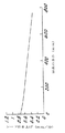
【0088】
さらに、サンプル4−7における結晶格子の空孔の濃度を、白金拡散技法を使用してマッピングした。白金濃度のウエハ表面からの深さ(0ミクロンの深さはウエハの前表面に対応する)に対するプロットを図5に示す。
【0089】
実施例2
本発明のプロセスが、チョクラルスキー成長のシリコンウエハに関して、酸素濃度に比較的依存しないことを明らかにするために、異なる酸素濃度を有する3枚のウエハを、実施例1に記載される同じ工程系列に供した。これらの各工程の条件、工程S1〜工程S4の前におけるウエハの初期酸素濃度(Oi)、工程S4の後でのウエハバルクの酸素析出密度(OPD)、および工程S4の後におけるウエハ表面から測定されるデニューデッドゾーンの深さ(DZ)を表IIに示す。図6、図7および図8は、得られたウエハの断面を示す(これらの図は、200倍の倍率で撮影された写真の拡大である);サンプル3−4を図6に示し、サンプル3−5を図7に示し、サンプル3−6を図8に示す。
【0090】
【表2】
表II
実施例3
本発明のプロセスが、酸素析出物安定化および成長工程(S4)のために使用される条件に比較的依存しないことを明らかにするために、同じ初期酸素濃度を有するウエハ(サンプル1−8)を、サンプル3−4に関する実施例2に記載される同じ工程系列に供した。しかし、市販の16Mb DRAMプロセスを、酸素析出物安定化および成長工程(S4)として使用した。図9は、得られたウエハの断面を示す(この図は、200倍の倍率で撮影された写真の拡大である)。工程S4の後において、サンプル1−8およびサンプル3−4は、匹敵し得るバルク酸素析出密度(サンプル1−8の7×10¹⁰/cm3対サンプル3−4の4×1010/cm3)および匹敵し得るデニューデッドゾーン深さ(約40ミクロン)を有した。
【0092】
実施例4
本実施例は、熱処理を行っているときに、バルクミクロ欠陥(BMD)密度、すなわち酸素析出化物の密度において、そして熱処理中における雰囲気中の酸素濃度の増大から生じるデニューデッドゾーン(DZ)の深さにおいて観測され得る傾向を例示する。3組の異なるウエハを、様々なプロセス条件下での急速熱アニーリング処理に供した。A組のウエハを1200℃で30秒間、窒素雰囲気下でアニーリング処理した;B組のウエハを同じ条件下で20秒間アニーリング処理した;C組のウエハを1200℃で30秒間、アルゴン雰囲気下でアニーリング処理した。予備酸化工程は、本実施例では3組のウエハのいずれに対しても行わなかった。
【0093】
下記の表IIIにより示されるように、酸素分圧を、所与の組の各ウエハに関して増大させた。アニーリング処理が完了すると、各ウエハのBMD密度およびDZ深さを、この分野で標準的な手段で測定した。結果を下記の表IIIに示す。
【0094】
【表3】
表III
【0095】
上記の結果は、雰囲気中の酸素分圧が増大すると、バルクミクロ欠陥の数密度が低下することを示している。さらに、酸素分圧が10,000ppmaに達すると、バルクミクロ欠陥の数密度は、本発明による事前の急速熱アニーリング処理を行うことなく酸素析出熱処理に供せられたウエハで観測されるバルクミクロ欠陥の数密度と区別することができない。
【0096】
軸対称領域を含有する単結晶シリコン
実施例5
所定のホットゾーン機構を有する結晶引き上げ装置の最適化手順
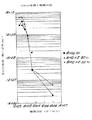
最初の200mmの単結晶シリコンインゴットを、結晶の長さに関して、引き上げ速度を0.75mm/分から約0.35mm/分に直線的に変化させた条件下で成長させた。図17は、結晶の長さを関数とする引き上げ速度を示す。結晶引き上げ装置内における成長中の200mmインゴットの以前に確立された軸温度特性と、平均軸温度勾配G0、すなわち、溶融/固体界面での軸温度勾配における以前に確立された半径方向の変化とを考慮して、このような引き上げ速度を選択して、インゴットが、中心からインゴットの一方の末端の縁まで空孔優勢材であり、そして中心からインゴットのもう一方の末端の縁まで格子間原子優勢材であることを確実にした。成長したインゴットを長さ方向にスライスし、凝集した格子間原子欠陥の生成がどこから始まっているかを決定するために分析した。
【0097】
図18は、欠陥分布パターンを明らかにする一連の酸素析出熱処理を行った後のインゴットの肩から約635mm〜約760mmの範囲の断面に関して、インゴットの軸切断面の少数キャリア寿命を走査することによって得られた像である。約680mmの結晶位置で、凝集した格子間原子欠陥280のバンドを認めることができる。この位置は、v*(680mm)=0.33mm/分の臨界引き上げ速度に対応する。この点において、軸対称領域60(格子間原子優勢材であるが、凝集した格子間原子欠陥を有さない領域)の幅はその最大値である;空孔優勢領域80の幅RV *(680)は約35mmであり、軸対称領域の幅RI *(680)は約65mmである。
【0098】
次いで、一連の4個の単結晶シリコンインゴットを、最初の200mmインゴットの軸対称領域の最大幅が得られた引き上げ速度よりも若干大きな定常的な引き上げ速度、およびそれよりも若干小さい定常的な引き上げ速度で成長させた。図19は、1〜4とそれぞれ記された4個の各結晶の結晶の長さを関数とする引き上げ速度を示す。次いで、これらの4個の結晶を分析して、凝集した格子間原子欠陥が最初に現れるかまたは消失する軸位置(および対応する引き上げ速度)を決定した。これらの4つの実験的に決定された点(「*」を付ける)を図19に示す。これらの点からの内挿および外挿によって、図19においてv*(Z)と印を付けた曲線が得られる。この曲線は、最初の近似に対して、軸対称領域がその最大幅である結晶引き上げ装置における長さを関数とする200mm結晶に関する引き上げ速度を表す。
他の引き上げ速度でのさらなる結晶の成長およびこのような結晶のさらなる分析により、v*(Z)の実験的な定義をさらに精密化する。
【0099】
実施例6
G0(r)における半径方向変化の低下
図20および図21は、溶融/固体界面での軸温度勾配G0(r)の半径方向変化の減少によって達成され得る品質の改善を例示する。空孔および格子間原子の(溶融/固体界面から約1cmでの)初期濃度を、2つの場合について、異なるG0(r)を用いて計算した:(1)G0(r)=2.65+5×10−4r2(K/mm)および(2)G0(r)=2.65+5×10−5r2(K/mm)。それぞれの場合について、引き上げ速度を、空孔が多いシリコンと格子間原子が多いシリコンとの境界が3cmの半径のところに位置するように調節した。場合1および場合2のために使用した引き上げ速度は、それぞれ、0.4mm/分および0.35mm/分であった。図21から、結晶の格子間原子が多い部分における格子間原子の初期濃度は、初期軸温度勾配の半径方向の変化が減少すると、劇的に減少することが明らかである。これにより、格子間原子の過飽和による格子間原子欠陥クラスターの生成を回避することがより容易になるために材料品質は改善される。
【0100】
実施例7
格子間原子に関する増加した外方拡散時間
図22および図23は、格子間原子の外方拡散に必要な時間を増大させることによって達成され得る品質の改善を例示する。格子間原子の初期濃度を、2つの場合について、結晶において異なる軸温度特性dT/dzを用いて計算した。溶融/固体界面での軸温度勾配は両方の場合について同じであり、その結果、格子間原子の(溶融/固体界面から約1cmでの)初期濃度は両方の場合について同じである。本実施例において、引き上げ速度を、結晶全体が、格子間原子が多くなるように調節した。引き上げ速度は、両方の場合について同じであり、0.32mm/分であった。場合2における格子間原子の外方拡散に必要な時間が長いほど、格子間原子濃度の全体的な減少が得られる。これにより、格子間原子の過飽和による格子間原子欠陥クラスターの生成を回避することがより容易になるために材料品質は改善される。
【0101】
実施例8
長さが700mmで、直径が150mmの結晶を、様々な引き上げ速度で成長させた。引き上げ速度を、段部(肩部)での約1.2mm/分から、段部(肩部)から430mmのところでの約0.4mm/分までほぼ直線的に変化させ、次いで、段部から700mmのところでの約0.65mm/分にまでほぼ直線的に戻した。この特定の結晶引き上げ装置におけるこのような条件下において、半径全体を、結晶の段部から約320mm〜約525mmの範囲の結晶の長さにわたって、格子間原子が多い条件下で成長させた。図24を参照して、約525mmの軸位置および約0.47mm/分の引き上げ速度で、結晶は、直径全体にわたって、凝集した真性点欠陥クラスターを含まない。言い換えれば、軸対称領域の幅、すなわち、凝集した欠陥を実質的に含まない領域の幅がインゴットの半径に等しい結晶の小さな部分が存在する。
【0102】
実施例9
実施例5に示すように、一連の単結晶シリコンインゴットを様々な引き上げ速度で成長させ、次いで、凝集した格子間原子欠陥が最初に現れるか消失する軸位置(および対応する引き上げ速度)を決定するために分析した。軸位置に対して引き上げ速度をグラフにプロットしたこれらの点からの内挿および外挿によって、第1の近似に対して、軸対称領域がその最大幅である結晶引き上げ装置における長さを関数とする200mmの結晶に関する引き上げ速度を示す曲線が得られた。次いで、さらなる結晶を他の引き上げ速度で成長させ、これらの結晶のさらなる分析を使用して、この実験的に決定した最適な引き上げ速度特性の精度を上げた。
【0103】
この結果を使用し、そしてこの最適な引き上げ速度特性に従って、長さが約1000mmで、直径が約200mmの結晶を成長させた。次いで、成長させた結晶の、様々な軸位置から得られたスライス物を、(i)凝集した格子間原子欠陥が生成しているかどうかを決定するために、そして(ii)スライス物の半径を関数としてV/I境界の位置を決定するために、この分野で標準的な酸素析出法を使用して分析した。このように、軸対称領域の存在を、結晶の長さまたは位置を関数としてこの領域の幅と同様に決定した。
【0104】
インゴットの肩から約200mm〜約950mmの範囲の軸位置に関して得られた結果を図25のグラフに示す。これらの結果は、引き上げ速度特性が、単結晶シリコンインゴットの成長に関して、インゴットの直径一定部分が、直径一定部分の半径の少なくとも約40%の長さである幅(周囲縁からインゴットの中心軸に向かって半径方向に測定される)を有する軸対称領域を含有するように決定され得ることを示す。さらに、これらの結果は、この軸対称領域が、インゴットの直径一定部分の長さの約75%の長さである長さ(インゴットの中心軸に沿って測定される)を有し得ることを示す。
【0105】
実施例10
長さが約1100mmで、直径が約150mmの単結晶シリコンインゴットを、引き上げ速度を低下させて成長させた。インゴットの直径一定部分の肩での引き上げ速度は約1mm/分であった。引き上げ速度を、肩から約200mmの軸位置に対応する約0.4mm/分にまで指数関数的に低下させた。次いで、引き上げ速度を、約0.3mm/分の速度がインゴットの直径一定部分の終端付近で得られるまで直線的に低下させた。
【0106】
この特定のホットゾーン配置でのこのようなプロセス条件下において、得られたインゴットは、軸対称領域が、インゴットの半径にほぼ等しい幅を有する領域を含有した。次に、一連の酸素析出熱処理を行った後のインゴットの一部の軸切断面の少数キャリア寿命を走査することによって得られた像である図26aおよび図26bを参照して、軸位置が約100mm〜約250mmおよび約250mm〜約400mmの範囲であるインゴットの連続領域が存在する。軸位置が肩から約170mm〜約290mmの範囲にあり、直径全体にわたって凝集した真性点欠陥を含まない領域がインゴット内に存在することがこれらの図から認めることができる。言い換えれば、軸対称領域の幅、すなわち、凝集した格子間原子欠陥を実質的に含まない領域の幅がインゴットの半径にほぼ等しい領域がインゴット内に存在する。
【0107】
さらに、軸位置から、約125mm〜約170mmの範囲および約290mm〜400mmを超える部分の範囲の領域において、凝集した真性点欠陥を含まず、凝集した真性点欠陥を同様に含まない空孔優勢材の一般にはシリンダー状コアを囲む格子間原子優勢材の軸対称領域が存在する。
【0108】
最後に、軸位置から、約100mm〜約125mmの範囲の領域において、凝集した欠陥を含まず、空孔優勢材の一般にはシリンダー状コアを囲む格子間原子優勢材の軸対称領域が存在する。空孔優勢材の内部において、凝集した欠陥を含まず、凝集した空孔欠陥を含有するコアを囲む軸対称領域が存在する。
【0109】
実施例11
冷却速度およびV/I境界の位置
一連の単結晶シリコンインゴット(150mmおよび200mmの公称直径)を、チョクラルスキー法に従って、約1050℃を超える温度でシリコンの滞留時間に影響を与える異なるホットゾーン配置(この分野での一般的な手段により設計)を使用して成長させた。各インゴットの引き上げ速度特性をインゴットの長さに沿って変化させ、凝集した空孔の点欠陥領域から凝集した格子間点欠陥領域に転移させることを試みた。
【0110】
一旦成長させ、インゴットを、成長方向に平行する中心軸に沿って長さ方向に切断し、次いで、それぞれが約2mmの厚さの部分にさらに分割した。次いで、前記の銅デコレーション技法を使用して、そのような長さ方向の部分の1組を加熱し、銅をわざと混入させた。加熱条件は、高濃度の銅格子間原子を溶解させるのに適していた。次いで、このような熱処理の後に、サンプルを急冷した。この間に、銅不純物は、酸化物クラスター、または存在する場合には、凝集した格子間原子欠陥の部位で外方拡散するかまたは析出した。標準的な欠陥ディリニエーションエッチングを行った後に、サンプルを析出不純物について目視で検査した;そのような析出不純物を含まないそのような領域は、凝集した格子間原子欠陥を含まない領域に対応した。
【0111】
長さ方向の部分の別組を、キャリア寿命マッピングの前に新しい酸化物クラスターの核形成および成長を行うために一連の酸素析出熱処理に供した。寿命マッピングにおけるコストラストバンドを、各インゴットにおける様々な軸位置での瞬間的な溶融/固体界面の形状の決定および測定を行うために利用した。次いで、溶融/固体界面の形状に関する情報を使用して、下記においてさらに考察するように、平均軸温度勾配G0の絶対値およびその半径方向の変化を推定した。この情報はまた、引き上げ速度とともにv/G0の半径方向の変化を推定するために使用された。
【0112】
単結晶シリコンインゴットの得られる品質に対する成長条件の効果をより詳細に調べるために、今日までの実験的証拠に基づいて妥当と考えられるいくつかの仮定を行った。最初に、格子間原子欠陥の凝集が生じる温度にまで冷却するのに要した時間に関する熱履歴の処理を単純化するために、約1050℃は、シリコン自己格子間原子の凝集が生じる温度に関して合理的な近似であると仮定した。この温度は、異なる冷却速度が用いられる実験を行っているときに観測された凝集した格子間原子の欠陥密度での変化と一致するようである。上記のように、凝集が生じるかどうかは、格子間原子濃度の因子でもあるが、凝集は、約1050℃を超える温度では生じないと考えられる。なぜなら、格子間原子濃度の範囲がチョクラルスキー型の成長プロセスに典型的であるならば、この系は、この温度より高い温度で、格子間原子により臨界的に過飽和にならないと仮定することは妥当であるからである。言い換えれば、チョクラルスキー型の成長プロセスに典型的な格子間原子濃度に関して、系は約1050℃を超える温度で臨界的に過飽和にならない、従って、凝集事象は生じないと仮定することは妥当である。
【0113】
単結晶シリコンの品質に対する成長条件の効果をパラメーター化するために行った第2の仮定は、シリコン自己格子間原子の拡散係数の温度依存性は無視できるということである。言い換えれば、自己格子間原子は、約1400℃と約1050℃との間のすべての温度で同じ速度で拡散すると仮定する。約1050℃は、凝集の温度に関して妥当な近似と見なされると理解すると、この仮定の本質的な点は、融点からの冷却曲線の細部は問題とならないということである。拡散距離は、融点から約1050℃までの冷却に費やされた総時間にだけに依存する。
【0114】
各ホットゾーン機構に関する軸温度特性データおよび特定のインゴットに関する実際の引き上げ速度特性を使用して、約1400℃から約1050℃までの総冷却時間を計算することができる。温度は各ホットゾーンに関して変化する速度はかなり均一であったことに注意しなければならない。この均一性は、凝集した格子間原子欠陥に必要な核形成温度(すなわち、約1050℃)の選択における何らかの誤差は、議論の余地はあるが、計算された冷却時間における誤差を比例的に増減させるだけであることを意味する。
【0115】
インゴットの空孔優勢領域の半径方向の拡がり(Rvacancy)、あるいは軸対称領域の幅を決定するために、空孔優勢コアの半径は、寿命マッピングによって決定されるように、v/G0=v/G0臨界である凝固での点に等しいとさらに仮定した。言い換えれば、軸対称領域の幅は、一般的には、室温に冷却した後のV/I境界の位置に基づくと仮定した。これは、上記のように、インゴットが冷えると、空孔とシリコン自己格子間原子との再結合が生じ得るので注目される。再結合が生じるとき、V/I境界の実際の位置は、インゴットの中心軸に向かって内側に移動する。本明細書で示されているのはこの最終的な位置である。
【0116】
凝固時の結晶における平均軸温度勾配G0の計算を単純化するために、溶融/固体界面の形状は融点等温線であると仮定した。結晶の表面温度を、有限要素モデル化(FEA)技法およびホットゾーン機構の細部を使用して計算した。結晶内の全体の温度場、従ってG0を、ラプラス式を適切な境界条件、すなわち、溶融/固体界面に沿った融点および結晶軸に沿った表面温度に関するFEA結果を用いて解くことによって得た。調製および評価を行ったインゴットの1つから様々な軸位置で得られる結果を図27に示す。
【0117】
格子間原子の初期濃度に対するG0の半径方向の効果を評価するために、半径方向の位置R’、すなわち、V/I境界と結晶表面との間の途中の位置は、シリコン自己格子間原子がインゴットにおいてシンクから離れ得る最も遠い点であると仮定したが、そのようなシンクは、空孔優勢領域に存在するか、または結晶表面に存在するかにはよらない。上記のインゴットに関する成長速度およびG0データを使用することによって、位置R’で計算されたv/G0とV/I境界でのv/G0(すなわち、臨界v/G0値)との差は、過剰な格子間原子が結晶表面上のシンクまたは空孔優勢領域でのシンクに達し得ることに対する効果および格子間原子の初期濃度での半径方向の変化を示す。
【0118】
この特定のデータ組に関して、結晶の品質は、全体的には、v/G0での半径方向の変化に依存していないようである。図28から明らかであり得るように、インゴットにおける軸依存性はこのサンプルで最小である。この実験系列に含まれる成長条件は、G0の半径方向の変化においてかなり狭い範囲を示す。結果として、このデータ組は狭すぎて、G0の半径方向の変化に対する品質(すなわち、凝集した真性点欠陥の有無)の認識可能な依存性を解明することができない。
【0119】
上記のように、調製した各インゴットのサンプルを、凝集した格子間原子欠陥の有無について様々な軸位置で評価した。調べた各軸位置に関して、サンプルの品質と軸対称領域の幅との間に相関が存在し得る。次に、図29を参照して、サンプルが、そのような特定の軸位置において、凝固から約1050℃に冷却された時間に対する所与サンプルの品質を比較するグラフを得ることができる。予想されるように、このグラフは、軸対称領域の幅(すなわち、Rcrystal−Rvacancy)が、この特定の温度範囲におけるサンプルの冷却履歴に強く依存していることを示す。軸対称領域の幅が大きくなるに従って、より長い拡散時間またはより遅い冷却速度が必要であるという傾向が示唆される。
【0120】
このグラフに示されるデータに基づいて、この特定の温度範囲内における所与インゴット直径に可能な冷却速度の関数として、「良好」(すなわち、無欠陥)から「不良」(すなわち、欠陥含有)までのシリコンの品質での転移を一般的に示す最良の近似線を計算することができる。軸対称領域の幅と冷却速度との間の一般的な関係は、下記の式で表すことができる:
(Rcrystal−Rtransition)2 = Deff *t1050℃
【0121】
上式において、
Rcrystalは、インゴットの半径であり、
Rtransitionは、無欠陥部から欠陥含有部まで、あるいはその逆の格子間原子優勢材において転移が生じるサンプルの軸位置での軸対称領域の半径であり、
Deffは、格子間原子拡散係数の平均時間および温度を表す定数で、約9.3*10−4cm2sec−1であり、そして
t1050℃は、サンプルの所与の軸位置が凝固から約1050℃に冷却されるのに必要な時間である。
【0122】
再度、図29を参照して、所与のインゴット直径に関して、冷却時間を、所望する直径の軸対称領域を得るために推定できることが理解され得る。例えば、約150mmの直径を有するインゴットに関して、インゴットの半径にほぼ等しい幅を有する軸対称領域は、約1410℃〜約1050℃の温度範囲域で、インゴットのこの特定部分が約10時間〜約15時間で冷却される場合に得ることができる。同様に、約200mmの直径を有するインゴットに関して、インゴットの半径にほぼ等しい幅を有する軸対称領域は、この温度範囲域で、インゴットのこの特定部分が約25時間〜約35時間で冷却される場合に得ることができる。この線がさらに外挿される場合、約65時間〜約75時間の冷却時間が、約300mmの直径を有するインゴットの半径にほぼ等しい幅を有する軸対称領域を得るために必要とされ得る。この点に関して、インゴットの直径が大きくなるに従って、格子間原子がインゴット表面または空孔コアでシンクに達するために拡散しなければならない距離が増大するために、さらなる冷却時間が必要であることに注意しなければならない。
【0123】
次に、図30、図31、図32および図33を参照して、様々なインゴットに関する冷却時間の増加による効果を認めることができる。これらの図のそれぞれは、凝固温度から1050℃までの冷却時間が図30から図33まで段階的に増大した公称直径が200mmのインゴットの一部を示す。
【0124】
図30を参照して、軸位置が肩から約235mm〜約350mmの範囲にあるインゴットの一部を示す。約255mmの軸位置において、凝集した格子間原子欠陥を含まない軸対称領域の幅は最大であり、インゴットの半径の約45%である。この領域を超えると、そのような欠陥を含まない領域から、そのような欠陥が存在する領域への転移が生じる。
【0125】
次に、図31を参照して、軸位置が肩から約305mm〜約460mmの範囲にあるインゴットの一部を示す。約360mmの軸位置において、凝集した格子間原子欠陥を含まない軸対称領域の幅は最大であり、インゴットの半径の約65%である。この領域を超えると、欠陥生成が始まる。
【0126】
次に、図32を参照して、軸位置が肩から約140mm〜約275mmの範囲にあるインゴットの一部を示す。約210mmの軸位置において、軸対称領域の幅は、インゴットの半径にほぼ等しい;すなわち、この範囲内のインゴットの小部分は、凝集した真性点欠陥を含まない。
【0127】
次に、図33を参照して、軸位置が肩から約600mm〜約730mmの範囲にあるインゴットの一部を示す。約640mm〜約665mmの範囲の軸位置に関して、軸対称領域の幅は、インゴットの半径にほぼ等しい。さらに、軸対称領域の幅がインゴットの半径にほぼ等しいインゴットのセグメントの長さは、図32のインゴットについて観測されるものよりも長くなっている。
【0128】
従って、図30、図31、図32および図33を組み合わせて見た場合、これらの図は、1050℃への冷却時間の欠陥を含まない軸対称領域の幅および長さに対する効果を明らかにしている。一般に、結晶の引き上げ速度の連続的な低下によって、結晶の一部の冷却時間に基づいて低下させるには大きすぎる格子間物の初期濃度が導かれ、結果的に、凝集した格子間欠陥を含有する領域が生じる。軸対称領域の長さが大きくなることは、より大きな範囲の引き上げ速度(すなわち、格子間原子の初期濃度)を、欠陥を含まないそのような材料に関して得ることができることを意味する。冷却時間の増大は、格子間原子のより大きな初期濃度を可能にする。なぜなら、半径方向の拡散に充分な時間が達成され、その濃度を格子間原子欠陥の凝集に必要とされる臨界濃度よりも低く抑えることができるからである。言い換えれば、冷却時間が長くなる場合には、幾分遅い引き上げ速度(および、従って、格子間原子のより高い初期濃度)によっても、依然として最大の軸対称領域60が得られる。従って、冷却時間を長くすると、最大の軸対称領域の直径に必要とされる条件について種々の引き上げ速度に対する許容度が大きくなり、プロセス制御に対する制限が少なくなる。結果として、インゴットのより大きな長さ部分にわたる軸対称領域についてのプロセスが一層容易になる。
【0129】
再度、図33を参照すると、結晶の肩の約665mmから730mmを超えるところまでの範囲の軸位置に関して、凝集した欠陥を含まない空孔優勢材の領域が存在し、その領域におけるその領域の幅はインゴットの半径に等しい。
【0130】
上記の結果から明らかであり得るように、冷却速度を制御することにより、自己格子間原子濃度は、それらが消滅し得る領域に格子間原子が拡散するのにより多くの時間を可能にすることによって抑制され得る。結果として、凝集した格子間原子欠陥の形成が、単結晶シリコンインゴットの大部分において防止される。
【0131】
上記を参照して、本発明のいくつかの目的が達成されることが理解される。
様々な変化を、本発明の範囲から逸脱することなく、上記の構成およびプロセスにおいて行うことできるので、上記の説明に含まれるすべての事項は、例示として解釈されるものであり、限定する意味で解釈されるものではない。
【図面の簡単な説明】
【図1】 本発明の方法の模式図である。
【図2】 実施例1に記載のように製造されたウエハ(サンプル4−7)の断面の写真である。
【図3】 実施例1に記載の一連の段階に曝露されたウエハ(サンプル4−8)の断面の写真である。
【図4】 実施例1に記載の一連の段階に曝露されたウエハ(サンプル3−14)の断面の写真である。
【図5】 実施例1に記載の一連の段階に曝露されたウエハ(サンプル4−7)の、表面からの深さに対する白金濃度(原子/cm3)の対数のグラフである。
【図6】 実施例2に記載の一連の段階に曝露されたウエハ(サンプル3−4)の断面の写真である。
【図7】 実施例2に記載の一連の段階に曝露されたウエハ(サンプル3−5)の断面の写真である。
【図8】 実施例2に記載の一連の段階に曝露されたウエハ(サンプル3−6)の断面の写真である。
【図9】 実施例3に記載の一連の段階に曝露されたウエハ(サンプル1−8)の断面の写真である。
【図10】 実施例4に記載のような、本発明の単結晶シリコンウエハの急速な熱アニールの間に、大気中に存在する酸素の分圧に対する、バルクミクロ欠陥(BMD)の数密度の対数グラフである。
【図11】 自己格子間原子[I]および空孔[V]の初期濃度が、比率v/G0[vは成長速度であり、G0は平均軸温度勾配である。]の数値の増加に伴って、変化する例を示すグラフである。
【図12】 自己格子間原子[I]の所定初期濃度に関して温度Tが低下するに伴って、凝集格子間原子欠陥の形成に必要とされる自由エネルギーの変化ΔGIが増加する例を示すグラフである。
【図13】 G0の数値の増加によって比率v/G0の数値が減少するに伴って、自己格子間原子[I]および空孔[V]の初期濃度が、ウエハのインゴットの半径に沿って変化する例を示すグラフである。
【図14】 それぞれ優勢材料の空孔Vおよび自己格子間原子Iの領域、ならびそれらの間に存在するV/I境界を示す単結晶シリコンインゴットまたはウエハの正面図である。
【図15】 インゴットの直径一定部分の軸対称領域を詳細に示す、単結晶シリコンインゴットの縦断面図である。
【図16】 空孔優勢材料のほぼ筒状の領域、自己格子間優勢材料のほぼ環状の軸対称領域、それらの間に存在するV/I境界、および凝集格子間原子欠陥の領域を詳細に示す、一連の酸素析出熱処理後のインゴットの軸方向カットの少数担体寿命のスキャンによって得られる画像である。
【図17】 引き上げ速度が、結晶の長さの一部において線状に減少することを示す、結晶の長さの関数としての引き上げ速度(即ち、種の引き上げ)のグラフである。
【図18】 実施例5に記載のような、一連の酸素析出熱処理後の、インゴットの軸方向カットの少数担体寿命のスキャンによって得られる画像である。
【図19】 実施例5に記載のような、v*(Z)で示される曲線を得るために使用される、それぞれ1〜4で示される4つの単結晶シリコンにおける、結晶の長さの関数としての引き上げ速度のグラフである。
【図20】 実施例6に記載の2種類の場合における、半径方向位置の関数としての、メルト/固体界面G0における平均軸方向温度勾配のグラフである。
【図21】 実施例6に記載の2種類の場合における、半径方向位置の関数としての、空孔「V」および自己格子間原子「I」の初期濃度のグラフである。
【図22】 実施例7に記載の2種類の場合における、インゴットにおける軸方向温度輪郭を示す、軸方向位置の関数としての温度のグラフである。
【図23】 図22に示され、実施例7にさらに詳しく記載される2種類の冷却条件から得られる自己格子間原子濃度のグラフである。
【図24】 実施例8に記載のような、一連の酸素析出熱処理後の、全インゴットの軸方向カットの少数担体寿命のスキャンによって得られる画像である。
【図25】 実施例9に記載のような、単結晶シリコンインゴットの長さの関数としての、V/I境界の位置を示すグラフである。
【図26a】 実施例10に記載のような、一連の酸素析出熱処理後の、インゴットのショルダーから約100mm〜約250mmにわたるインゴットのセグメントの軸方向カットの少数担体寿命のスキャンによって得られる画像である。
【図26b】 実施例10に記載のような、一連の酸素析出熱処理後の、インゴットのショルダーから約250mm〜約400mmにわたるインゴットのセグメントの軸方向カットの少数担体寿命のスキャンによって得られる画像である。
【図27】 実施例11に記載のような、インゴットの種々の軸方向位置における、軸方向温度勾配G0のグラフである。
【図28】 実施例11に記載のような、インゴットの種々のものにおける、平均軸方向温度勾配G0における半径方向変化のグラフである。
【図29】 実施例11に記載のような、軸対称領域の幅と冷却速度の関係を示すグラフである。
【図30】 実施例11に記載のような、銅デコレーション(copper decoration)および欠陥ディリニエーションエッチング(defect−delineating etch)後の、インゴットのショルダーから約235mm〜約350mmにわたるインゴットのセグメントの軸方向カットの写真である。
【図31】 実施例11に記載のような、銅デコレーションおよび欠陥ディリニエーションエッチング後の、インゴットのショルダーから約305mm〜約460mmにわたるインゴットのセグメントの軸方向カットの写真である。
【図32】 実施例11に記載のような、銅デコレーションおよび欠陥ディリニエーションエッチング後の、インゴットのショルダーから約140mm〜約275mmにわたるインゴットのセグメントの軸方向カットの写真である。
【図33】 実施例11に記載のような、銅デコレーションおよび欠陥ディリニエーションエッチング後の、インゴットのショルダーから約600mm〜約730mmにわたるインゴットのセグメントの軸方向カットの写真である。
【図34】 種々の形態のホットゾーン(hot zones)において生じる平均軸方向温度勾配G0(r)における半径方向変化を示すグラフである。
【図35】 4種類のホットゾーン形態におけるインゴットの軸方向温度輪郭を示すグラフである。[0001]
BACKGROUND OF THE INVENTION
The present invention relates generally to semiconductor material substrates, particularly silicon wafers, used in the manufacture of electronic components. In particular, the present invention forms oxygen precipitates of ideal non-uniform depth distribution and substantially has agglomerated intrinsic point defects during the thermal treatment cycle of essentially any electronic device manufacturing process. The present invention relates to a silicon wafer additionally having a non-axially symmetric region and a manufacturing method thereof.
[0002]
[Prior art]
Single crystal silicon, which is the starting material for most methods of manufacturing semiconductor electronic components, is generally manufactured by the so-called Czochralski method, in which a single seed crystal is immersed in molten silicon and then grown by slow extraction. As molten silicon is loaded into the quartz crucible, it is contaminated by various impurities, mainly oxygen. At the temperature of the silicon melt mass, oxygen enters the crystal lattice until it reaches a concentration measured by the solubility of oxygen in the silicon at the temperature of the melt mass and the effective segregation coefficient of oxygen in the solidified silicon. Such a concentration is greater than the solubility of oxygen in solid silicon at temperatures common to electronic device manufacturing processes. Crystals grow from the molten mass and cool, thus rapidly reducing the solubility of oxygen therein, so that oxygen is present at a supersaturated concentration in the resulting slice or wafer.
[0003]
Thermal processing cycles commonly used in the manufacture of electronic devices can cause oxygen precipitation in silicon wafers supersaturated with oxygen. Depending on the location of the deposition on the wafer, the deposition can be harmful or beneficial. Oxygen deposition located in the active device region of the wafer can impair device operation. However, oxygen precipitation present in the bulk can trap undesirable metallic impurities that contact the wafer. The use of oxygen precipitation located in the bulk of the wafer to capture the metal is commonly referred to as internal gettering or intrinsic gettering (IG).
[0004]
Historically, electronic device manufacturing processes are referred to as zones or regions (generally referred to as “denewed zones” or “no deposition zones”) that do not have oxygen precipitates near the surface of the wafer. And the remainder of the wafer, ie the wafer bulk, includes a series of steps designed to produce silicon with a sufficient number of oxygen precipitates for the IG. The denewed zone is, for example, (a) oxygen external diffusion heat treatment for at least about 4 hours in an inert atmosphere at high temperature (> 1100 ° C.), (b) oxygen precipitation nucleation at low temperature (600 ° C. to 750 ° C.) And (c) oxygen (SiO2) at high temperature (1000 ° C. to 1150 ° C.)2It can be formed in a high temperature-low temperature-high temperature thermal sequence such as)) precipitate growth. For example, F. Shimura,Semiconductor Silicon Crystal Technology, Academic Press, Inc., San Diego Calofornia (1989), p361-367, and references cited therein.
[0005]
Recently, however, advanced electronic device manufacturing methods, such as DRAM manufacturing methods, have come to minimize the use of high temperature process steps. Some of these processes still use high temperature process steps to form denewed zones and sufficiently dense bulk deposits, but the tolerance for such materials is very low and is not commercially available. It cannot be a product that can survive. Other current highly advanced electronic device manufacturing methods do not include any external diffusion steps. Because of the problems associated with oxygen precipitation in the active device region, these electronic device manufacturers must use silicon wafers that do not form oxygen precipitates anywhere on the wafer under process conditions. As a result, all possibilities of IG are lost.
[0006]
[Problems to be solved by the invention]
Accordingly, it is an object of the present invention to provide a single crystal silicon wafer that forms oxygen precipitates with an ideal non-uniform depth distribution during the heat treatment cycle of essentially any electronic device manufacturing process; Providing a wafer that optimally and reproducibly forms sufficient density of oxygen precipitates in the wafer de-newed zone and wafer bulk; formation of the de-new zone and oxygen precipitate formation in the wafer bulk Providing a wafer that does not depend on the difference in oxygen concentration in the region; Providing a method in which the formation of a denewed zone does not depend on oxygen out-diffusion; Providing wafers that are essentially independent; formation of denewed zones and formation of oxygen precipitates in the wafer bulk Providing a wafer that is not affected by thermal history and oxygen concentration of a Czochralski-grown single crystal silicon ingot from which the silicon wafer is sliced; and defects resulting from aggregation of crystal lattice vacancies or silicon self-interstitials Providing a wafer additionally having a substantially radial axisymmetric region substantially free of;
[0007]
[Means for Solving the Problems]
Briefly, therefore, the present invention relates to two generally parallel major surfaces, one on the front surface of the wafer and the other on the back surface of the wafer; a central plane between the front and back surfaces; A peripheral edge joining the surfaces; a distance D of at least about 10 micrometers measured from the front surface to the center plane1And a bulk layer comprising a second region of the wafer between the central plane and a first region. In particular, the wafer has a non-uniform distribution of crystal lattice vacancies, and the concentration of vacancies in the bulk layer is greater than the concentration of vacancies in the surface layer. Or a concentration profile that exists in the vicinity and generally decreases in concentration from the peak density position toward the front surface of the wafer. In one embodiment, the wafer additionally has a first axisymmetric region in which the vacancies are dominant intrinsic point defects and substantially free of agglomerated intrinsic point defects, the first axisymmetric region Comprises a central axis or has a width of at least about 15 mm. In another embodiment, the wafer additionally has an axially symmetric region that is substantially free of agglomerated intrinsic point defects, the axially symmetric region extending radially inward from the peripheral edge of the wafer. And having a width measured radially from the peripheral edge toward the central axis, the width being at least about 40% of the length of the radius of the wafer.
[0008]
The present invention includes two substantially parallel major surfaces, one on the front surface of the wafer and the other on the back surface of the wafer; a central plane between the front and back surfaces; a peripheral edge joining the front and back surfaces; Distance D of about 15 micrometers or less on the front surface2It also relates to a single crystal silicon wafer having a front surface layer comprising a region of the wafer within; a bulk layer comprising a region of the wafer between the central plane and the front surface layer. In particular, when the wafer is exposed to an oxygen precipitation heat treatment consisting essentially of annealing the wafer at 800 ° C. for 4 hours and then at 1000 ° C. for 16 hours, the peak density of precipitates in the bulk layer is Substantially uniform oxygen concentration and crystal lattice vacancies such that the wafer contains oxygen precipitates present in the vicinity and having a concentration profile in which the concentration of precipitates in the bulk layer generally decreases in the direction of the front surface layer The bulk layer has a concentration of In one embodiment, the wafer additionally has a first axisymmetric region in which the vacancies are dominant intrinsic point defects and substantially free of agglomerated intrinsic point defects, the first axisymmetric region Comprises a central axis or has a width of at least about 15 mm. In another aspect, the wafer additionally comprises an axially symmetric region substantially free of agglomerated intrinsic point defects, the axially symmetric region extending radially inward from the peripheral edge of the wafer. And having a width measured radially from the peripheral edge toward the central axis, the width being at least about 40% of the length of the radius of the wafer.
[0009]
The present invention includes two substantially parallel major surfaces, one on the front surface of the wafer and the other on the back surface of the wafer; a central plane between the front and back surfaces; and a perimeter that joins the front and back surfaces Also relates to a single crystal silicon wafer having an edge. A distance D containing interstitial oxygen and measured from the front surface to the central plane from the front surface to at least 10 micrometers1The wafer is characterized by having a denewed zone comprising a region of the wafer. The wafer is D1It is also characterized in that the concentration of interstitial oxygen in the denewed zone at a distance corresponding to one-half of this is at least about 75% of the maximum concentration of interstitial oxygen in the denewed zone. In one embodiment, the wafer is also characterized in that the wafer comprises a first axisymmetric region that is a dominant intrinsic point defect and substantially free of agglomerated intrinsic point defects, wherein the first axisymmetric The region has a central axis or has a width of at least about 15 mm. In another embodiment, the wafer comprises an axially symmetric region that is substantially free of agglomerated intrinsic point defects, the axially symmetric region extending radially inward from a peripheral edge of the wafer. , And a width measured radially from the peripheral edge toward the central axis, the width being at least about 40% of the length of the radius of the wafer.
[0010]
The present invention further joins two substantially parallel major surfaces, one on the front surface of the wafer and the other on the back surface of the wafer; a central plane between the front and back surfaces; and the front and back surfaces Perimeter edge; distance D of about 15 micrometers or less on the front surface2It also relates to a single crystal silicon wafer having a front surface layer comprising a region of the wafer within; and a bulk layer comprising a region of the wafer between the central plane and the front surface layer. In particular, when the wafer is exposed to an oxygen precipitation heat treatment consisting essentially of annealing the wafer at 800 ° C. for 4 hours and then at 1000 ° C. for 16 hours, the peak density of precipitates in the bulk layer is Substantially uniform oxygen concentration and crystal lattice vacancies such that the wafer contains oxygen precipitates present in the vicinity and having a concentration profile in which the concentration of precipitates in the bulk layer generally decreases in the direction of the front surface layer The bulk layer has a concentration of
[0011]
The present invention further relates to a method of heat treating a Cz single crystal silicon wafer to affect the precipitation behavior of oxygen on the wafer in a later thermal processing stage. The wafer has a front surface; a rear surface; a central plane between the front and rear surfaces; a vacancy sink at the front surface; a front surface and a distance D measured from the front surface toward the central plane1A front surface layer comprising a region of the wafer between the central plane and the distance D measured from the front surface of the wafer1A bulk layer comprising a region of the wafer between; and an axisymmetric region substantially free of agglomerated intrinsic point defects. In this method, the wafer is heat-treated to form crystal lattice vacancies in the wafer. Next, the concentration of vacancies in the heat-treated wafer is reduced by adjusting the cooling rate of the heat-treated wafer so that the peak density is at or near the center plane and the concentration is at the front surface of the wafer. A wafer having a vacancy concentration profile that generally decreases in the direction of is formed. The difference in the concentration of vacancies in the front surface layer and the bulk layer is such that the heat treatment of the wafer at a temperature higher than 750 ° C. leads to the formation of the denewed zone in the front surface layer and the formation of oxygen clusters or precipitates in the bulk zone. The difference is that the concentration of oxygen clusters or precipitates mainly depends on the concentration of vacancies in the bulk layer.
[0012]
Other objects and features of the invention will be apparent in part and will be set forth in part below.
[0013]
In accordance with the present invention, an ideal deposition wafer has been found. This wafer essentially forms a denewed zone that is deep enough for IG purposes and a wafer bulk that contains oxygen precipitates of sufficient density during any electronic device manufacturing process. This ideal deposition wafer can be conveniently prepared in a short time using tools commonly used in the semiconductor silicon manufacturing industry. Such processing determines the manner in which oxygen precipitates during the electronic device manufacturing process or forms a “template” on the silicon that “prints”.
[0014]
The ideal starting material for the deposition wafer of the present invention is a single crystal wafer sliced from a single crystal ingot grown according to conventional Czochralski crystal growth methods. Such methods are similar to standard silicon slicing, lapping, etching and polishing techniques, eg, F. Shimura,Semiconductor Silicon Crystal Technology, Academic Press (1989), andSilicon Chemical Etching (Edited by J. Grabmaier) Springer-Verlag, New York (1982) (these are incorporated herein by reference). Czochralski-grown silicon is typically about 5 × 10¹⁷Atom / cm3~ About 9 × 10¹⁷Atom / cm3It has an oxygen concentration within the range of (ASTM standard F-121-83). Since the oxygen precipitation behavior of the wafer is not intrinsically linked to the oxygen concentration in the ideal deposition wafer, the oxygen concentration of the starting wafer can be any concentration within the range that can be reached by the Czochralski process or its concentration. There can even be any concentration outside the range.
[0015]
Depending on the cooling rate of the single crystal silicon ingot from the melting point (about 1410 ° C.) temperature of the silicon to the range of about 750 ° C. to about 350 ° C., the nucleation center of the oxygen precipitate is the single crystal silicon into which the wafer is sliced. Can be formed into an ingot. However, the presence or absence of such nucleation centers in the starting material is not critical to the present invention if these centers can be dissolved by heat treating the silicon at a temperature not exceeding about 1300 ° C. Some heat treatments, such as annealing the silicon for about 4 hours at a temperature of about 800 ° C., stabilize these centers so that they cannot melt at a temperature not exceeding about 1150 ° C. Can do. The detection limit of oxygen precipitates is currently about 5 × 10⁶Precipitate / cm3It is. The presence (or density) of nucleation centers for oxygen precipitation cannot be measured directly using currently available techniques. However, its presence can be indirectly detected using various techniques. As mentioned above, the pre-existing oxygen precipitate nucleation center in silicon can be stabilized and the precipitate can be grown at such sites by subjecting the silicon to an oxygen precipitation heat treatment. it can. Thus, the presence of such nucleation centers can be measured indirectly after an oxygen precipitation heat treatment, such as a wafer annealing process at a temperature of 800 ° C. for 4 hours and then at a temperature of 1000 ° C. for 16 hours. it can.
[0016]
When the substituted carbon is present as an impurity in single crystal silicon, it has a catalytic ability to form an oxygen precipitation nucleation center. Thus, for these and other reasons, it is preferred that the single crystal silicon starting material has a low concentration of carbon. That is, single crystal silicon is about 5 × 10¹⁶Atom / cm3Less, preferably about 1 × 10¹⁶Atom / cm3Less, more preferably about 5 × 10¹⁵Atom / cm3Having a carbon concentration of less than
[0017]
Next, referring to FIG. 1, a single
[0018]
In the first embodiment of the process of the present invention, the
[0019]
Process S2The wafer is subjected to a heat treatment process in which the wafer is heated to a high temperature to form crystal lattice vacancies (vacancy points) 13 in the
[0020]
In the first embodiment of the present invention, the rapid thermal annealing step is performed in a nitride-forming atmosphere, that is, nitrogen gas (N2) Or an atmosphere containing a nitrogen-containing compound gas (such as ammonia) that can turn the exposed silicon surface into a nitride. Accordingly, such an atmosphere can be entirely composed of nitrogen gas or nitrogen compound gas. Alternatively, such an atmosphere can further include a non-nitride forming gas such as argon. Increasing the vacancy concentration (vacancy point concentration) of the entire wafer, if not immediately, is almost achieved when the annealing temperature is reached. The wafer is generally at this temperature for at least 1 second, typically at least several seconds (eg, at least 3 seconds), preferably tens of seconds (eg, 20 seconds, 30 seconds, 40 seconds or 50 seconds), and Depending on the desired properties of the wafer, it is held for a period of time that can range up to about 60 seconds (which is about the limit of commercial rapid thermal annealing equipment). The resulting wafer has relatively uniform vacancy concentration (number density) characteristics in this wafer.
[0021]
Based on experimental evidence obtained to date, the atmosphere in which the rapid thermal annealing process is performed preferably has only a relatively small partial pressure of oxygen, water vapor and other oxidizing gases; The atmosphere is not sufficient to inject a sufficient amount of silicon self-interstitials to suppress the growth of vacancy concentration, with no oxidizing gas present or no partial pressure of such gas. is there. Although the lower limit concentration of the oxidizing gas has not been determined accurately, an increase in the vacancy concentration and the effect are observed with respect to an oxygen partial pressure of 0.01 atm, ie 10,000 parts / million atoms (ppma). It has been clarified that Accordingly, the atmosphere preferably has a partial pressure of oxygen and other oxidizing gases of less than 0.01 atm (10,000 ppma); more preferably, the partial pressure of these gases in the atmosphere is about 0.002 atm ( 2,000 ppma) or less, more preferably about 0.005 atm (5,000 ppma) or less, and most preferably about 0.001 atm (1,000 ppma) or less.
[0022]
In addition to the formation of crystal lattice vacancies, the rapid thermal annealing process dissolves any unstabilized oxygen precipitate nucleation centers present in the silicon starting material. Such nucleation centers can be formed, for example, during the growth of a single crystal silicon ingot into which the wafer is sliced, or some other event in the previous thermal history of the wafer or ingot into which the wafer is sliced. As a result it can be formed. Thus, the presence or absence of such nucleation centers in the starting material is not important if these centers can be dissolved during the rapid thermal annealing process.
[0023]
The rapid thermal annealing process can be performed in any of a number of commercially available rapid thermal annealing (“RTA”) processing furnaces in which the wafers are individually heated by a series of high power light sources. The RTA furnace can heat silicon wafers rapidly. For example, an RTA furnace can heat a wafer from room temperature to 1200 ° C. in a few seconds. One such commercially available RTA furnace is the model 610 furnace available from AG Associates (Mountain View, CA).
[0024]
Intrinsic point defects (vacancies and silicon self-interstitials) can diffuse through single crystal silicon at a temperature dependent diffusion rate. Thus, the concentration characteristics of intrinsic point defects are a function of the intrinsic point defect diffusion coefficient and recombination rate as a function of temperature. For example, intrinsic point defects can move relatively close to the temperature at which the wafer is annealed in the rapid thermal annealing process, but at temperatures as high as 700 ° C., essentially in any commercially practical time. I can't move. Based on experimental evidence obtained so far, the effective diffusion rate of vacancies can be quite slow at temperatures below about 700 ° C. and possibly as high as 800 ° C. or 900 ° C. or even 1000 ° C. It is suggested. The vacancies can be regarded as not moving in any commercially practical time.
[0025]
Process S2When the process is completed, the wafer passes through a temperature range in which the crystal lattice vacancies can move relatively in the single crystal silicon (or to the temperature range).3Quenched in When the temperature of the wafer drops past this range of temperatures, the vacancies diffuse into the
[0026]
Process S4The wafer is subjected to an oxygen precipitation heat treatment. For example, the wafer can be annealed at a temperature of 800 ° C. for 4 hours and then at a temperature of 1000 ° C. for 16 hours. Alternatively, the wafer is preferably placed in a furnace at a temperature of about 800 ° C. as in the first step of the electronic device manufacturing process. When placed in a furnace at this temperature, the rapid thermal annealed wafer has different zones that behave differently with respect to oxygen precipitation. In the high vacancy area (wafer bulk), oxygen clusters rapidly when the wafer is placed in the furnace. By the time the load temperature is reached, the clustering process is complete, resulting in a cluster distribution that depends only on the initial concentration of vacancies. In the low vacancy region (near the wafer surface), the wafer behaves like a normal wafer with no pre-existing oxygen precipitate nucleation centers; ie, no oxygen clustering is observed. When the temperature rises above 800 ° C. or when the temperature is kept constant, the clusters in the zone with more vacancies grow and precipitate and are consumed thereby, but in the zone with fewer vacancies Nothing happens. By dividing the wafer into various zones of vacancy concentration, a template is effectively obtained, which draws an oxygen precipitate pattern that is fixed when the wafer is placed in the furnace.
[0027]
As illustrated in FIG. 1, the resulting depth distribution of oxygen precipitates on the wafer does not include oxygen precipitates extending from the
[0028]
The concentration of oxygen precipitates in
[0029]
The respective depths t and t ′ from the front and rear surfaces of the materials (denewed zones) 15 and 15 ′ that do not contain oxygen precipitates are mainly due to the relative movement of the crystal lattice vacancies in the silicon. It is a function of the cooling rate to the temperature range obtained. Generally, the depth t, t ′ increases with decreasing cooling rate, and the depth of the denewed zone is at least about 10 microns, 20 microns, 30 microns, 40 microns, 50 microns, 70 microns, or even 100 microns. You can get it. Importantly, the depth of the denewed zone is essentially independent of the details of the electronic device manufacturing process and, in addition, is dependent on the traditionally performed out-diffusion of oxygen. do not do.
[0030]
The rapid thermal treatment used in the process of the present invention allows a small amount of oxygen to diffuse out from the front and back surfaces of the wafer, while the amount of out-diffusion is observed in conventional processes for the generation of denewed zones. Significantly less than the amount to be used. As a result, the ideal deposition wafer of the present invention has a substantially uniform interstitial oxygen concentration as a function of distance from the silicon surface. For example, prior to performing the oxygen precipitation heat treatment, the wafer may have a substantially uniform interstitial oxygen concentration from the wafer center to a wafer area within about 15 microns of the wafer surface, more preferably from the silicon center to the wafer surface. Up to a wafer area within about 10 microns, even more preferably, from the center of silicon to a wafer area within about 5 microns of the wafer surface, most preferably from the center of silicon to a wafer area within about 3 microns of the wafer surface. Have. As used herein, a substantially uniform oxygen concentration means that the dispersion of oxygen concentration is less than about 50%, preferably less than about 20%, and most preferably less than about 10%. And
[0031]
Typically, due to the oxygen precipitation heat treatment, a substantial amount of oxygen does not diffuse out of the heat-treated wafer. As a result, the interstitial oxygen concentration in the denewed zone at a distance exceeding several microns from the wafer surface does not change significantly as a result of the precipitation heat treatment. For example, the distance D at which the denewed zone of the wafer is measured from the silicon surface and from the front surface toward the center plane.1(Which is at least about 10 microns)1The oxygen concentration at a point in the denewed zone at a distance from the silicon surface equal to ½ of is typically the maximum interstitial oxygen concentration at any location within the denewed zone. At least about 75% of the concentration. For some oxygen precipitation heat treatments, the interstitial oxygen concentration at this location is greater, ie, at least 85% or 90% of the maximum oxygen concentration anywhere in the denewed zone, or Even 95% of that.
[0032]
In the second embodiment of the present invention, a non-nitride forming atmosphere is used instead of the nitride forming atmosphere used in the heating (rapid thermal annealing) and cooling steps of the first embodiment. The Suitable non-nitriding atmospheres include argon, helium, neon, carbon dioxide and other such non-oxidizing, non-nitriding elemental and compound gases, or mixtures of such gases. included. Such a non-nitride-forming atmosphere is a relatively low partial pressure of oxygen, that is, less than 0.01 atm (10,000 ppma), more preferably 0.005 atm (5 Less than 0.002 atm (2,000 ppma), most preferably less than 0.001 atm (1,000 ppma).
[0033]
In the third embodiment of the present invention, step S1The (thermal oxidation step) is omitted and the starting wafer has only a natural oxide layer. However, when such a wafer is annealed in a nitrogen atmosphere, the effect is that a wafer having a thicker oxide layer ("incremental oxide layer") than the native oxide layer is annealed in nitrogen. This is different from the effect that is observed when When a wafer containing an incremental oxide layer is annealed in a nitrogen atmosphere, a substantially uniform increase in vacancy concentration is achieved across the entire wafer, if not immediately after the annealing temperature is reached. Furthermore, the vacancy concentration does not appear to increase significantly as a function of the annealing time at a given annealing temperature. However, if the wafer has only a native oxide layer and the front and back surfaces of the wafer are annealed in nitrogen, the resulting wafer has approximately “U-shaped” voids with respect to the wafer cross-section. Concentration (number density) characteristics; that is, the maximum concentration is within a few microns of the front and back surfaces, and a relatively constant lower concentration is present throughout the wafer bulk. Its minimum concentration in the wafer bulk is initially approximately equal to that obtained with a wafer having an incremental oxide layer. Furthermore, increasing the annealing time increases the vacancy concentration in wafers having only a natural oxide layer.
[0034]
Experimental evidence indicates that the difference between the behavior of a wafer with only a native oxide layer and that of an incremental oxide layer is avoided by including molecular oxygen or other oxidizing gases in the atmosphere. It is further suggested that it can be done. In other words, when a wafer with only native oxide is annealed in a nitrogen atmosphere containing a low oxygen partial pressure, the wafer behaves in the same way as a wafer with an incremental oxide layer. Without being bound by any theory, a surface oxide layer that is thicker than a native oxide layer appears to serve as a shield that inhibits silicon nitridation. Accordingly, such an oxide layer can be present on the surface of the starting wafer or can be formed in-situ during processing by growing an incremental oxide layer during the annealing process.
[0035]
Thus, according to the present invention, the atmosphere in the rapid thermal annealing step preferably comprises a partial pressure of at least about 0.0001 atm (100 ppma), more preferably at least about 0.0002 atm (200 ppma). However, for the reasons described above, the oxygen partial pressure preferably does not exceed 0.01 atm (10,000 ppma), more preferably is less than 0.005 atm (5,000 ppma), and still more preferably is 0.00. Less than 002 atm (2,000 ppma), most preferably less than 0.001 atm (1,000 ppma).
[0036]
In other embodiments of the present invention, the front and back surfaces of the wafer can be exposed to different atmospheres. Each of the atmospheres can contain one or more nitriding or non-nitriding gases. For example, the back surface of the wafer can be exposed to a non-nitriding gas while the front surface is exposed to a non-nitriding gas. Alternatively, multiple wafers (eg, two, three or more wafers) can be simultaneously annealed while being stacked with their faces facing each other; when annealed in this manner, they face each other The contacting surfaces are mechanically shielded from the atmosphere during the annealing process. Alternatively, depending on the atmosphere used in the rapid thermal annealing process and the desired oxygen precipitation characteristics of the wafer, the oxide layer is formed only on the wafer surface where a de-newed zone is desired, eg, the
[0037]
The starting material for the process of the present invention can be a polished silicon wafer or a non-polished silicon wafer that has been lapped and etched. Further, the wafer may have vacancies or self-interstitial point defects as the dominant intrinsic point defects. For example, the wafer is surrounded by dominating vacancies from center to edge, predominating self-interstitial atoms from center to edge, or surrounded by an axisymmetric annular self-interstitial dominant material. It may contain a central core of vacancy dominant material.
[0038]
More specifically, referring now to FIG. 15, such a wafer can be obtained from a single
[0039]
In one embodiment, the
[0040]
In another embodiment, such a wafer can be obtained from a single
[0041]
If the epitaxial layer can be deposited on an ideal deposition wafer, the process of the present invention can be performed before or after the epitaxial deposition. If the process of the present invention is performed before that, it may be desirable to stabilize the oxygen precipitate nucleation centers after the process of the present invention and before epitaxial deposition. If the process of the present invention is subsequently performed, it may be desirable to perform the process of the present invention in an epitaxial reactor immediately after epitaxial deposition if the cooling rate required by the process of the present invention can be achieved. obtain.
[0042]
Measurement of crystal lattice vacancies in single crystal silicon can be performed by platinum diffusion analysis. In general, platinum is deposited on a sample and diffused to a horizontal surface. The diffusion time and diffusion temperature at this time are preferably selected so that the diffusion of platinum is governed by the Frank-Turnbull mechanism, which is a decoration of vacancies by platinum atoms. It is sufficient to reach the steady state. For wafers having a typical vacancy concentration with respect to the present invention, a diffusion time and diffusion temperature of 20 minutes at 730 ° C. can be used, but a more accurate analysis can be performed at lower temperatures, eg, about 680 It seems that it can be obtained at ° C. In addition, to minimize the effects believed to be due to the silicide formation process, the platinum deposition method preferably provides a surface concentration of less than one monolayer. Platinum diffusion techniques are described elsewhere: eg Jacob et al.J. Appl. Phys.82, 182 (1997); Zimmermann and Ryssel, "Modeling of platinum diffusion in silicon under non-equilibrium conditions,"J. Electrochemical Society139, 256 (1992); Zimmermann, Goesele, Seilenthal and Eichiner, “Wafer Mapping of Void Concentration in Silicon”,Journal of Crystal Growth129, 582 (1993); Zimmermann and Falster, "Investigation of nucleation of oxygen precipitates in the early stages of Czochralski silicon",Appl. Phys. Lett.60, 3250 (1992); Zimmermann and Ryssel,Appl. Phys. A55, 121 (1992).
[0043]
Preparation of single crystal silicon containing axisymmetric regions
Based on experimental evidence to date, the type and initial concentration of intrinsic point defects can be determined based on the temperature at which the ingot is above the solidification temperature (ie, about 1410 ° C.) to 1300 ° C. (ie, at least about 1325 ° C., or at least about 1350). C., or at least about 1375.degree. C.). That is, the type and initial concentration of such defects is the ratio v / G0(V is the growth rate and G0Is the mean axial temperature gradient over this temperature range).
[0044]
Referring to FIG. 11, v / G0As the value increases, the transition from gradual self-interstitial dominant growth to vacant dominant growth is v / G0Occurs near the critical value of. This critical value is based on currently available information and is approximately 2.1 × 10⁻⁵cm2Seems to be / sK. In this case, G0Is measured under conditions where the axial temperature gradient is constant within the above temperature range. At this critical value, the concentration of these intrinsic point defects is balanced.
[0045]
v / G0When the value exceeds the critical value, the vacancy concentration increases. Similarly, v / G0When the value is smaller than the critical value, the self-interstitial concentration increases. If these concentrations reach the critical supersaturation level of the system, and if the mobility of point defects is sufficiently high, a reaction or agglomeration event can occur. The concentration of aggregated intrinsic point defects in silicon can have a significant impact on the expected yield of materials in the manufacture of complex highly integrated circuits.
[0046]
According to the present invention, there is a reaction in which vacancies in a silicon matrix react to generate aggregated vacancy defects, and a reaction in which self-interstitial atoms in the silicon matrix react to generate aggregated interstitial defects. It has been discovered that it can be suppressed. Without being bound by any particular theory, the concentration of vacancies and self-interstitial atoms is the change in free energy of the system during crystal ingot growth and cooling in the process of the present invention, It is considered that the agglomeration reaction occurs spontaneously and is controlled so as not to exceed the critical value at which agglomerated vacancy defects or interstitial defects are generated.
[0047]
In general, in single crystal silicon, a system that can be used to drive a reaction in which agglomerated vacancy defects are formed from vacancy point defects or a reaction in which agglomerated interstitial defects are formed from self-interstitial atoms. The change in free energy is governed by the following equation (1):
[Expression 1]
[In the above formula,
ΔGV / IIs the change in free energy for reactions that form agglomerated vacancy defects or reactions that form interstitial defects,
k is the Boltzmann constant,
T is the temperature in K,
[V / I] is the concentration of vacancies or interstitial atoms applied at one point in space and time in single crystal silicon,
[V / I]eqIs the equilibrium concentration of vacancies or interstitial atoms applied at temperature T at the same point in space and time where [V / I] exists. ]
[0049]
From this equation, for a given concentration [V] of vacancies, when the temperature T decreases, in general, ΔGV[V] with temperatureeqIncreases due to a sharp drop. Similarly, for a given concentration of interstitial atoms [I], as temperature T decreases, generally ΔGI[I] with temperatureeqIncreases due to a sharp drop.
[0050]
FIG. 12 shows ΔGIAnd schematically illustrate the silicon self-interstitial concentration for an ingot cooled from the solidification temperature without using several means simultaneously to suppress the silicon self-interstitial concentration. This is illustrated in When the ingot cools, ΔGIIncreases according to equation (1) due to an increase in the degree of supersaturation of [I] and approaches the energy barrier for the generation of aggregated interstitial defects. As cooling continues, this energy barrier is effectively exceeded, at which time a reaction occurs. As a result of this reaction, aggregated interstitial defects are generated and ΔG is reduced so that the supersaturated system is relaxed, ie, the [I] concentration is reduced.IAccompanied by a decline.
[0051]
Similarly, if the ingot is cooled from the solidification temperature without simultaneously using several means to control the vacancy concentration, ΔGVIncreases according to equation (1) due to the increased supersaturation of [V] and approaches the energy barrier for the formation of agglomerated vacancy defects. As cooling continues, this energy barrier is effectively exceeded, at which time a reaction occurs. As a result of this reaction, ΔG is generated so that agglomerated vacancy defects are generated and the supersaturated system is relaxed.VAccompanied by a decline.
[0052]
Agglomeration of vacancies and interstitial atoms occurs when the ingot is cooled from the solidification temperature by maintaining the free energy of the vacancies and interstitial systems at a value less than the value at which the agglomeration reaction occurs, respectively. It can be avoided in the region of the dominant material and the interstitial dominant material. That is, the system can be controlled such that vacancies or interstitial atoms are never critically supersaturated. This is low enough so that critical supersaturation is never achieved (v / G as defined below).0Can be achieved by establishing an initial concentration of vacancies and interstitial atoms (controlled by (r)). In practice, however, such concentrations are difficult to achieve throughout the crystal radius. Thus, in general, critical supersaturation occurs after crystal solidification, ie, v / G0This can be avoided by suppressing the initial vacancy concentration and initial interstitial concentration after establishing the initial concentration determined by (r).
[0053]
Surprisingly, generally about 10-4cm2Because of the relatively large mobility of self-interstitial atoms that are per second and to a lesser extent due to the mobility of vacancies, a relatively large distance, i.e. from about 5 cm to about 10 cm or more. Suppress interstitial atoms and vacancies by diffusing self-interstitial atoms radially to sinks located on the crystal surface or to vacancy-dominated regions located in the crystal It was found that it was possible. Radial diffusion should be used effectively to suppress the concentration of self-interstitials and vacancies if sufficient time is able to diffuse the initial concentration of intrinsic point defects radially. Can do. In general, the diffusion time depends on the radial change in the initial concentration of self-interstitials and vacancies. The smaller the change in the radial direction, the shorter the diffusion time.
[0054]
Average axial temperature gradient G0Typically increases with increasing radius for single crystal silicon grown according to the Czochralski method. This is v / G0A value typically means not single across the radius of the ingot. As a result of such changes, the type and initial concentration of intrinsic point defects are not constant. V / G indicated as V /
[0055]
When an ingot containing a V / I boundary is cooled from the solidification temperature, radial diffusion of interstitial atoms and vacancies causes the V / I boundary to radiate due to recombination of self-interstitial atoms and vacancies. Move inward in the direction. Furthermore, radial diffusion of self-interstitial atoms to the crystal surface occurs when the crystal cools. The crystal surface can maintain a substantially balanced point defect concentration as the crystal cools. The radial diffusion of point defects tends to reduce the concentration of self-interstitial atoms outside the V / I boundary and the concentration of vacancies inside the V / I boundary. Thus, if sufficient time is possible for diffusion, the concentration of vacancies and interstitial atoms everywhere is ΔGVAnd ΔGIHowever, it can be made smaller than the critical value at which the agglomeration reaction of vacancies and the agglomeration reaction of interstitial atoms occur.
[0056]
Referring to FIG. 15 again, the growth rate v and the average axis temperature gradient G0The crystal growth conditions including the cooling rate are preferably controlled so that the single
[0057]
The width of the
[0058]
Growth rate v and mean axial temperature gradient G (defined above)0Is typically the ratio v / G0But v / G0Controlled to be in the range of about 0.5 to about 2.5 times the critical value (ie, v / G0Based on currently available information on critical values, about 1 × 10⁻⁵cm2/ SK to about 5 × 10⁻⁵cm2/ SK). This ratio v / G0Is preferably v / G0Range from about 0.6 times to about 1.5 times the critical value (ie, v / G0Based on currently available information regarding critical values, about 1.3 × 10⁻⁵cm2/ SK to about 3 × 10⁻⁵cm2/ SK). This ratio v / G0Is most preferably v / G0Range from about 0.75 times to about 1.25 times the critical value (ie, v / G0Based on currently available information regarding critical values, approximately 1.6 × 10⁻⁵cm2/ SK-about 2.1 x 10⁻⁵cm2/ SK). In one particularly preferred embodiment, v / G in the
[0059]
In order to maximize the width of the
[0060]
Average shaft temperature gradient G0This can be achieved by designing the “hot zone” of the crystal puller, ie, in particular, the design of the graphite (or other material) that makes the heater, insulation, heat and radiation shield. The individual design can vary depending on the structure and type of the crystal puller, but in general G0Can be performed using any means currently known in the art to control heat transfer at the melt / solid interface. Such means include reflectors, radiation shields, purge tubes, light pipes and heaters. In general, G0The radial variation is minimized by placing such a device within about one crystal diameter above the melt / solid interface. G0Can be further controlled by adjusting the position of the apparatus relative to the melt and the crystals. This is accomplished by adjusting the position of the device in the hot zone or by adjusting the position of the molten surface in the hot zone. In addition, if a heater is used, G0Can be further adjusted by adjusting the power supplied to the heater. Any or all of these methods can be used when performing a batch Czochralski process where the melting capacity is lost during the process.
[0061]
Average shaft temperature gradient G0However, it is generally preferred for some embodiments of the present invention to be relatively constant as a function of ingot diameter. However, the hot zone mechanism is G0It should be noted that the mechanical problems associated with maintaining a constant growth rate become an increasingly important factor as it is improved to minimize changes in This makes the growth process even more sensitive to any changes in pulling speed that also directly affects the growth speed v. For process control, this is different in the ingot radius G0It means that it has a value. But G0The large difference in value results in a large concentration of self-interstitial atoms that increase almost towards the wafer edge, which can make it increasingly difficult to avoid the generation of aggregated intrinsic point defects.
[0062]
See above, G0For control of G0Balance between minimizing the radial variation of the process and maintaining favorable process control conditions. Therefore, typically, the pulling speed after a crystal length of about 1 diameter is in the range of about 0.2 mm / min to about 0.8 mm / min. The pulling rate is preferably in the range of about 0.25 mm / min to about 0.6 mm / min, more preferably in the range of about 0.3 mm / min to about 0.5 mm / min. It should be noted that the pulling speed depends on both the crystal diameter and the crystal pulling design. The above range is typical for a 200 mm diameter crystal. In general, the pulling rate decreases as the crystal diameter increases. However, the crystal pulling device can be designed such that the pulling speed exceeds the speed described herein. As a result, most preferably, the crystal pulling device is designed according to the present invention to make the pulling speed as fast as possible while still allowing the formation of one or more axisymmetric regions.
[0063]
The amount of self-interstitial diffusion determines the cooling rate when the ingot is cooled from the solidification temperature (about 1410 ° C.) to the temperature at which the silicon self-interstitials are immobilized, for commercially practical processes. It is controlled by controlling. It appears that silicon self-interstitial atoms can move extremely at temperatures near the solidification temperature of silicon (ie, about 1410 ° C.). However, this mobility decreases as the temperature of the single crystal silicon ingot decreases. In general, self-interstitial diffusion rates are those that are commercially viable at temperatures below about 700 ° C, and perhaps as high as 800 ° C, 900 ° C, 1000 ° C, or even 1050 ° C. Slow enough to essentially not move in a reasonable time.
[0064]
In this regard, the temperature at which the self-interstitial aggregation reaction theoretically occurs varies over a wide range of temperatures, but in practice this range is relatively narrow for conventional Czochralski grown silicon. There must be. This is a result of the initial concentration of self-interstitial atoms typically obtained in silicon grown by the Czochralski method in a relatively narrow range. Thus, in general, a self-interstitial agglomeration reaction, if any, can occur at a temperature in the range of about 1100 ° C. to about 800 ° C., typically at a temperature of about 1050 ° C.
[0065]
Depending on the temperature in the hot zone, the cooling rate typically ranges from about 0.1 ° C./min to about 3 ° C./min in the temperature range in which the self-interstitials can move. It is. The cooling rate is preferably in the range of about 0.1 ° C./min to about 1.5 ° C./min, more preferably in the range of about 0.1 ° C./min to about 1 ° C./min, and even more The range is preferably about 0.1 ° C./min to about 0.5 ° C./min.
[0066]
By controlling the cooling rate of the ingot to a temperature range where the self-interstitial atoms can move, the self-interstitial atoms multiply several times and diffuse into the sink located on the crystal surface or into the vacancy dominant region Where they can disappear. Therefore, the concentration of such interstitial atoms is suppressed and acts so that no aggregation event occurs. The use of the interstitial diffusion coefficient (diffusion rate) by controlling the cooling rate is an otherwise demanding v / G that may be required to obtain an axisymmetric region free of agglomerated defects.0Acts to relax the condition. In other words, as a result of the fact that the cooling rate can be controlled to allow the interstitial atoms to diffuse several times, a large range of v / G for the critical value.0Values can be accepted to obtain axisymmetric regions that do not contain agglomerated defects.
[0067]
In order to achieve such a cooling rate over a considerable length of a constant diameter portion of the crystal, considerations have been given to the ingot end cone growth process as well as to the ingot processing when the end cone growth has ended. Must be done in the same way as Typically, when growth of a constant diameter portion of the ingot is complete, the pulling rate is increased to begin the tapering required to form the end cone. However, such an increase in the pulling speed causes the lower region of the constant diameter portion to cool more rapidly within the temperature range in which the interstitial atoms can sufficiently move, as described above. As a result, these interstitial atoms do not have enough time to diffuse into sinks that can disappear. That is, the concentration in the lower region cannot be sufficiently suppressed, and interstitial atom defects can aggregate.
[0068]
Therefore, in order to prevent the formation of such defects in this lower region of the ingot, it is preferable that the constant diameter portion of the ingot has a uniform thermal history according to the Czochralski method. A uniform thermal history is relatively constant not only when growing a constant diameter portion, but also when growing a crystal end cone, and if possible after an end cone growth. This can be achieved by pulling the ingot from the silicon melt at a reduced speed. A relatively constant speed can be achieved, for example, by: (i) performing end cone growth relative to the crucible and crystal rotation speed when growing a constant diameter portion of the crystal. Reducing the rotation speed of the crucible and the crystal and / or (ii) growing the end cone against the power supplied conventionally when performing the end cone growth. Increasing the power supplied to the heater sometimes used to heat the silicon melt. These further adjustments of the process variables can be made individually or in combination.
[0069]
When starting to grow an end cone, the lifting speed of the end cone is established as follows. Any region of the constant diameter portion of the ingot that remains at a temperature above about 1050 ° C contains an axially symmetric region that does not contain agglomerated intrinsic point defects and is already cooled to a temperature below about 1050 ° C. It is designed to go through the same thermal history as other areas of constant diameter.
[0070]
As described above, there is a minimum radius of the vacancy dominant region, which can suppress agglomerated interstitial defects. The value of the minimum radius is v / G0Depends on (r) and the cooling rate. As the crystal pulling device and hot zone mechanism change, v / G0The range shown above for (r), the pulling rate and the cooling rate will also vary. Similarly, these conditions can vary along the length of the growing crystal. As noted above, the width of the interstitial dominant region that does not include aggregated interstitial defects is preferably maximized. Therefore, the width of this region should be as close as possible to the difference between the radius of the crystal and the minimum radius of the vacancy-dominated region along the length of the growing crystal in a given puller. It is desirable to maintain no value.
[0071]
The optimum width of the
[0072]
FIG. 16 is an image obtained by scanning the minority carrier lifetime of the axial cut surface of an ingot having a diameter of 200 mm after performing a series of oxygen precipitation heat treatments to reveal the defect distribution pattern. FIG. 16 shows an example where near-optimal pull rate characteristics are used in the hot zone mechanism of a given crystal puller. In this example, v / G exceeds the maximum width of the interstitial dominant region (resulting in the generation of a region of aggregated
[0073]
G over the radius of the ingot0V / G resulting from increasing0In addition to the radial change of v / G0Can also be obtained as a result of changing v or by the Czochralski process.0May change axially as a result of natural changes in For a standard Czochralski process, v is changed so that the pulling rate is adjusted throughout the growth cycle to maintain the ingot at a constant diameter. These adjustments or changes in the pulling speed are then v / G0Is varied over the length of the constant diameter portion of the ingot. Thus, with the process of the present invention, the pulling speed is controlled to maximize the width of the axisymmetric region of the ingot. However, as a result, the radius of the ingot can vary. Thus, to ensure that the resulting ingot has a constant diameter, it is preferred that the ingot be grown to a diameter that is larger than the desired diameter. The ingot is then subjected to standard processes in the field to remove excess material from the surface. In this way, an ingot having a constant diameter portion can be reliably obtained.
[0074]
Generally, shaft temperature gradient G0If the radial change of (r) is minimized, it is easier to produce a hole dominant material that does not contain agglomerated defects. With reference to FIG. 35, the axial temperature characteristics for four separate hot zone positions are illustrated. FIG. 34 shows the axial temperature gradient G from the center of the crystal to ½ of the crystal radius.0Represents the change in (r): This is determined by averaging the slope from the solidification temperature to the temperature shown on the x-axis. Crystals were observed in Ver. 1 and Ver. G marked 40When drawn in a hot zone with a larger radial change in (r), it is not possible to obtain a crystal having a vacancy dominant material free from agglomerated defects from the center to the edge of any axial length It was. However, the crystals are Ver. 2 and Ver. G marked 30When drawn in a hot zone with a smaller radial change in (r), a crystal having a void-dominant material from the center to the edge that does not contain agglomerated defects with respect to several axial lengths of the crystal. Could get.
[0075]
In one embodiment of the process of the present invention, the initial concentration of silicon self-interstitial atoms is controlled in the axisymmetric self-interstitial
[0076]
In another embodiment of the invention, v / G0Is controlled such that no V / I boundary exists along the radius for at least part of the length of the ingot. At this length, the silicon is vacant-dominated from the center to the peripheral edge, and the agglomerated vacancy defects are predominantly V / G0Can be avoided in an axisymmetric region extending radially inward from the peripheral edge of the ingot. That is, the growth conditions are controlled, and as a result, v / G0Is v / G0Critical value and v / G0It has a value included between 1.1 times the critical value.
[0077]
Visual detection of agglomerated defects
Aggregated defects can be detected by a number of different techniques. For example, flow pattern defects or D defects are typically detected by selectively etching a single crystal silicon sample in a Secco etchant for about 30 minutes, and then subjecting the sample to microscopy ( For example, see H. Yamagishi et al., Semicond. Sci. Technol. 7, A135 (1992)). Although this method is standard for detecting agglomerated vacancy defects, this method can also be used to detect agglomerated interstitial defects. When using this technique, such defects, if present, appear as large depressions at the sample surface.
[0078]
Aggregated defects can also be detected using laser scattering techniques such as laser scattering tomography. Laser scattering techniques typically have a lower defect density detection limit than other etching techniques.
[0079]
In addition, agglomerated intrinsic point defects can be detected visually by decorating these defects with a metal that can diffuse into the single crystal silicon matrix when heat is applied. Specifically, a single crystal silicon sample such as a wafer, slag or slab is obtained by first coating the surface of the sample with a composition containing a metal that can decorate these defects, such as a concentrated solution of copper nitrate. A visual inspection can be performed for the presence of such defects. The coated sample is then heated at a temperature between about 900 ° C. and about 1000 ° C. for about 5 minutes to about 15 minutes to diffuse the metal into the sample. The heat treated sample is then cooled to room temperature. In this way, the metal is critically supersaturated and deposited at sites in the sample matrix where defects are present.
[0080]
After cooling, the sample is first subjected to a defect-free dilination etch by treating the sample with an active etch solution for about 8 minutes to about 12 minutes to remove surface residues and precipitation agents. A typical active etch solution includes about 55% nitric acid (70 wt% solution), about 20% hydrofluoric acid (49 wt% solution) and about 25% hydrochloric acid (concentrated solution).
[0081]
The sample is then washed with deionized water and the sample is subjected to a second etching step by immersing or treating with Secco or Wright etchant for about 35 minutes to about 55 minutes. Provide. Typically, the sample is etched using a Secau etchant containing 0.15M potassium dichromate and hydrofluoric acid (49 wt% solution) in a ratio of about 1: 2. This etching step serves to reveal, i.e. outline, aggregated defects that may be present.
[0082]
In general, regions of interstitial and vacancy dominated materials that do not contain agglomerated defects can be distinguished from each other by the copper decoration technique described above, and can be distinguished from materials that contain agglomerated defects. The area of the interstitial dominant material that does not contain defects does not contain the decorated features revealed by etching, but does not contain defects (before performing the high temperature oxygen nucleation process described above). This region contains small etching recesses due to copper decoration of oxygen nuclei.
[0083]
Definition
As used herein, the following expressions or terms shall have the following meanings: “Agglomerated intrinsic point defects” refers to defects caused by: (i) vacancies agglomerate to form D defects, flow pattern defects, gate oxide integrity defects, crystals Reactions that produce particle defects of origin, crystal-origin light spot defects, and other such defects associated with vacancies, or (ii) self-interstitial atoms aggregate to dislocation loops and networks, and others Reactions that generate defects related to such self-interstitial atoms. “Aggregated interstitial defects” shall mean aggregated intrinsic point defects caused by a reaction in which silicon self-interstitials aggregate. “Agglomerated vacancy defects” shall mean agglomerated vacancy defects caused by a reaction in which the vacancies of the crystal lattice agglomerate. “Radius” means the distance measured from the central axis to the peripheral edge of the wafer or ingot. “The agglomerated intrinsic point defectsExistence“None” shall mean that the concentration of agglomerated defects is below the detection limit of these defects (the detection limit is currently about 103Defect / cm3Is). “V / I boundary” means a position along the ingot or wafer radius where the material changes from vacancy dominant to self-interstitial dominance. “Vacancy dominant” and “self-interstitial dominance” refer to materials in which intrinsic point defects are predominantly vacancies or self-interstitial atoms, respectively.
[0084]
【Example】
Examples 1 through 4 illustrate the ideal oxygen precipitation process of the present invention. As described above, Examples 5 to 11 are examples of single crystal silicon containing an axially symmetric region of a void-dominant material, a self-interstitial atom-dominant material, or both substantially free of aggregated intrinsic point defects. Illustrate the preparation. Accordingly, all of these examples should not be construed in a limiting sense.
[0085]
Ideal oxygen precipitation process
Example 1
A silicon single crystal was pulled up by the Czochralski method, sliced, and polished to obtain a silicon wafer. Then, these wafers are subjected to a surface oxidation step (S1), Rapid thermal annealing process in nitrogen or argon (S2) And quickly cooled (S3), And oxygen stabilization and growth steps under the conditions shown in Table I (S4). Process S1~ Process S4The initial oxygen concentration (Oi), Process S4Wafer bulk oxygen precipitate density (OPD), and step S4The depth of the denewed zone after (DZ) is also shown in Table I.
[0086]
[Table 1]
Table I
2, 3 and 4 show cross sections of the resulting wafers (these figures are magnified photographs taken at 200 × magnification); sample 4-7 is shown in FIG. 4-8 is shown in FIG. 3, and sample 3-14 is shown in FIG.
[0088]
In addition, the concentration of crystal lattice vacancies in Samples 4-7 was mapped using a platinum diffusion technique. A plot of platinum concentration versus depth from the wafer surface (0 micron depth corresponds to the front surface of the wafer) is shown in FIG.
[0089]
Example 2
In order to demonstrate that the process of the present invention is relatively independent of oxygen concentration with respect to Czochralski grown silicon wafers, three wafers with different oxygen concentrations were subjected to the same steps described in Example 1. Served for series. Conditions for each step, step S1~ Process S4The initial oxygen concentration (Oi), Process S4Oxygen Precipitation Density (OPD) of Wafer Bulk after Step S, and Step S4The depth (DZ) of the denewed zone measured from the wafer surface after is shown in Table II. 6, 7 and 8 show cross sections of the resulting wafer (these figures are magnified photographs taken at 200 × magnification); sample 3-4 is shown in FIG. 3-5 is shown in FIG. 7, and sample 3-6 is shown in FIG.
[0090]
[Table 2]
Table II
Example 3
The process of the present invention provides oxygen precipitate stabilization and growth steps (S4A wafer having the same initial oxygen concentration (sample 1-8) is subjected to the same process described in Example 2 for sample 3-4. Served for series. However, a commercially available 16 Mb DRAM process is used to stabilize and grow the oxygen precipitate (S4) Was used. FIG. 9 shows a cross section of the resulting wafer (this figure is an enlargement of a photograph taken at 200 × magnification). Process S4After, Sample 1-8 and Sample 3-4 are comparable bulk oxygen precipitation densities (7 × 10¹⁰/
[0092]
Example 4
This example shows the denuded zone (DZ) resulting from an increase in the bulk microdefect (BMD) density, ie the density of oxygen precipitates, and the concentration of oxygen in the atmosphere during the heat treatment when heat treatment is performed. Illustrates trends that can be observed in depth. Three sets of different wafers were subjected to rapid thermal annealing processes under various process conditions. Group A wafers were annealed at 1200 ° C. for 30 seconds in a nitrogen atmosphere; Group B wafers were annealed for 20 seconds under the same conditions; Group C wafers were annealed at 1200 ° C. for 30 seconds in an argon atmosphere Processed. The pre-oxidation step was not performed on any of the three sets of wafers in this example.
[0093]
As shown by Table III below, the oxygen partial pressure was increased for each wafer in a given set. Once the annealing process was complete, the BMD density and DZ depth of each wafer was measured by standard means in this field. The results are shown in Table III below.
[0094]
[Table 3]
Table III
[0095]
The above results show that the number density of bulk micro defects decreases as the oxygen partial pressure in the atmosphere increases. Furthermore, when the oxygen partial pressure reaches 10,000 ppma, the number density of bulk micro defects is observed in the wafer subjected to the oxygen precipitation heat treatment without the prior rapid thermal annealing treatment according to the present invention. It cannot be distinguished from the number density.
[0096]
Single crystal silicon containing axisymmetric regions
Example 5
Optimization procedure for crystal pulling equipment with a predetermined hot zone mechanism
The first 200 mm single crystal silicon ingot was grown under conditions where the pulling rate was varied linearly from 0.75 mm / min to about 0.35 mm / min with respect to the crystal length. FIG. 17 shows the pulling rate as a function of crystal length. Pre-established axial temperature characteristics of the growing 200 mm ingot in the crystal puller and the average axial temperature gradient G0I.e., considering the previously established radial change in the axial temperature gradient at the melt / solid interface and choosing such a pull-up speed, the ingot is edged from the center to one end of the ingot. It was ensured that it was a vacancy dominant material, and an interstitial dominance material from the center to the edge of the other end of the ingot. The grown ingot was sliced lengthwise and analyzed to determine where the generation of aggregated interstitial defects began.
[0097]
FIG. 18 shows the minority carrier lifetime of the axial section of the ingot for a cross section ranging from about 635 mm to about 760 mm from the shoulder of the ingot after performing a series of oxygen precipitation heat treatments that reveal the defect distribution pattern. It is the obtained image. A band of aggregated
[0098]
Then, a series of four single crystal silicon ingots were steadily lifted slightly higher than the pulling speed at which the maximum width of the axisymmetric region of the first 200 mm ingot was obtained, and slightly lower than that. Grow at speed. FIG. 19 shows the pulling speed as a function of the crystal length of each of the four crystals labeled 1-4. These four crystals were then analyzed to determine the axial position (and corresponding pulling speed) at which aggregated interstitial defects first appear or disappear. These four experimentally determined points ("*") Is shown in FIG. By interpolation and extrapolation from these points, v in FIG.*A curve marked (Z) is obtained. This curve represents, for the first approximation, the pulling speed for a 200 mm crystal as a function of the length in the crystal pulling apparatus whose axisymmetric region is its maximum width.
With further crystal growth at other pulling rates and further analysis of such crystals, v*Further refine the experimental definition of (Z).
[0099]
Example 6
G0Reduced radial change in (r)
20 and 21 show the axial temperature gradient G at the melt / solid interface.0Illustrates the quality improvements that can be achieved by reducing the radial variation of (r). The initial concentration of vacancies and interstitial atoms (at about 1 cm from the melt / solid interface) is different for the two cases0Calculated using (r): (1) G0(R) = 2.65 + 5 × 10⁻⁴r2(K / mm) and (2) G0(R) = 2.65 + 5 × 10⁻⁵r2(K / mm). In each case, the pulling rate was adjusted so that the boundary between silicon with many vacancies and silicon with many interstitial atoms was located at a radius of 3 cm. The pulling speeds used for
[0100]
Example 7
Increased outward diffusion time for interstitial atoms.
22 and 23 illustrate the quality improvement that can be achieved by increasing the time required for out-diffusion of interstitial atoms. The initial concentration of interstitial atoms was calculated for the two cases using different axial temperature characteristics dT / dz in the crystal. The axial temperature gradient at the melt / solid interface is the same for both cases, so that the initial concentration of interstitial atoms (at about 1 cm from the melt / solid interface) is the same for both cases. In this example, the pulling rate was adjusted so that the entire crystal had more interstitial atoms. The pulling speed was the same for both cases and was 0.32 mm / min. The longer the time required for out-diffusion of interstitial atoms in
[0101]
Example 8
Crystals having a length of 700 mm and a diameter of 150 mm were grown at various pulling speeds. The pulling speed is changed almost linearly from about 1.2 mm / min at the step (shoulder) to about 0.4 mm / min at 430 mm from the step (shoulder), and then 700 mm from the step. It returned almost linearly to about 0.65 mm / min. Under such conditions in this particular crystal puller, the entire radius was grown under high interstitial conditions over the length of the crystal ranging from about 320 mm to about 525 mm from the crystal step. Referring to FIG. 24, at an axial position of about 525 mm and a pulling speed of about 0.47 mm / min, the crystal does not contain aggregated intrinsic point defect clusters throughout the diameter. In other words, there is a small portion of the crystal in which the width of the axisymmetric region, ie the width of the region substantially free of agglomerated defects, is equal to the radius of the ingot.
[0102]
Example 9
As shown in Example 5, a series of single crystal silicon ingots are grown at various pulling rates, and then the axial position (and corresponding pulling rate) at which aggregated interstitial defects first appear or disappear is determined. Analyzed for. By interpolation and extrapolation from these points plotting the pulling speed against the axial position in the graph, the length in the crystal pulling device whose axisymmetric region is its maximum width is a function of the first approximation. A curve showing the pulling speed for a 200 mm crystal was obtained. Additional crystals were then grown at other pulling rates and further analysis of these crystals was used to increase the accuracy of this experimentally determined optimal pulling rate characteristic.
[0103]
This result was used and crystals having a length of about 1000 mm and a diameter of about 200 mm were grown according to this optimum pulling speed characteristic. The grown crystals are then sliced from various axial positions, (i) to determine if aggregated interstitial defects are generated, and (ii) the slice radius is To determine the position of the V / I boundary as a function, analysis was performed using standard oxygen precipitation methods in the field. Thus, the presence of the axisymmetric region was determined as a function of the crystal length or position as well as the width of this region.
[0104]
The results obtained for axial positions ranging from about 200 mm to about 950 mm from the shoulder of the ingot are shown in the graph of FIG. These results show that the pulling speed characteristic is related to the growth of the single crystal silicon ingot in that the constant diameter part of the ingot is at least about 40% the length of the constant diameter part radius (from the peripheral edge to the central axis of the ingot). It can be determined to contain axisymmetric regions with (measured radially towards). Furthermore, these results show that this axisymmetric region can have a length (measured along the central axis of the ingot) that is approximately 75% of the length of the constant diameter portion of the ingot. Show.
[0105]
Example 10
A single crystal silicon ingot having a length of about 1100 mm and a diameter of about 150 mm was grown at a reduced pulling speed. The pulling speed at the shoulder of the constant diameter portion of the ingot was about 1 mm / min. The pulling speed was reduced exponentially to about 0.4 mm / min corresponding to an axial position of about 200 mm from the shoulder. The pulling speed was then reduced linearly until a speed of about 0.3 mm / min was obtained near the end of the constant diameter portion of the ingot.
[0106]
Under such process conditions in this particular hot zone configuration, the resulting ingot contained a region where the axisymmetric region had a width approximately equal to the radius of the ingot. Next, referring to FIGS. 26a and 26b, which are images obtained by scanning the minority carrier lifetime of a part of the axial cut surface of the ingot after a series of oxygen precipitation heat treatments, the axial position is approximately There are continuous regions of ingots that range from 100 mm to about 250 mm and from about 250 mm to about 400 mm. It can be seen from these figures that the axial position is in the range of about 170 mm to about 290 mm from the shoulder, and that there is a region within the ingot that does not contain intrinsic point defects aggregated over the entire diameter. In other words, there exists a region in the ingot in which the width of the axially symmetric region, that is, the width of the region that does not substantially contain the aggregated interstitial defects is substantially equal to the radius of the ingot.
[0107]
Further, in the region from the axial position in the range of about 125 mm to about 170 mm and in the range of more than about 290 mm to 400 mm, there is no agglomerated intrinsic point defect, and there is no agglomerated intrinsic point defect similarly In general, there is an axially symmetric region of interstitial dominant material surrounding the cylindrical core.
[0108]
Finally, in the region ranging from about 100 mm to about 125 mm from the axial position, there is an axisymmetric region of the interstitial dominant material that does not contain agglomerated defects and generally surrounds the cylindrical core of the void-dominant material. Within the vacancy dominant material, there is an axisymmetric region surrounding the core that does not contain agglomerated defects and that contains agglomerated vacancy defects.
[0109]
Example 11
Cooling rate and V / I boundary position
A series of single crystal silicon ingots (150 mm and 200 mm nominal diameters), according to the Czochralski method, have different hot zone arrangements that affect the residence time of silicon at temperatures above about 1050 ° C. (a common means in the field Developed using The pulling speed characteristic of each ingot was changed along the length of the ingot, and an attempt was made to transfer from the point defect region of the agglomerated holes to the agglomerated interstitial point defect region.
[0110]
Once grown, the ingot was cut lengthwise along a central axis parallel to the growth direction and then further divided into portions each about 2 mm thick. Then, using the copper decoration technique described above, one set of such lengthwise portions was heated to intentionally incorporate copper. The heating conditions were suitable for dissolving a high concentration of copper interstitial atoms. The sample was then quenched after such heat treatment. During this time, copper impurities diffused out or precipitated at the sites of oxide clusters or, if present, agglomerated interstitial defects. After performing standard defect delineation etching, the samples were visually inspected for precipitated impurities; such regions that did not contain such precipitated impurities corresponded to regions that did not contain aggregated interstitial defects. .
[0111]
Another set of longitudinal sections was subjected to a series of oxygen precipitation heat treatments to nucleate and grow new oxide clusters prior to carrier lifetime mapping. The cost-last band in lifetime mapping was used to determine and measure the instantaneous melt / solid interface shape at various axial positions in each ingot. The information about the shape of the melt / solid interface is then used to determine the mean axial temperature gradient G, as discussed further below.0The absolute value of and its radial change were estimated. This information can also be seen along with the pulling speed v / G0It was used to estimate the radial change of.
[0112]
In order to investigate in more detail the effect of growth conditions on the resulting quality of single crystal silicon ingots, we made several assumptions that are considered reasonable based on experimental evidence to date. Initially, in order to simplify the processing of the thermal history with respect to the time taken to cool to the temperature at which interstitial defect aggregation occurs, about 1050 ° C. is reasonable with respect to the temperature at which silicon self-interstitial aggregation occurs. It was assumed that This temperature appears to be consistent with the change in the defect density of agglomerated interstitial atoms observed when conducting experiments where different cooling rates are used. As described above, whether or not agglomeration occurs is also a factor of the interstitial concentration, but it is considered that agglomeration does not occur at temperatures exceeding about 1050 ° C. Because, if the range of interstitial concentrations is typical for Czochralski-type growth processes, it is assumed that the system does not become critically supersaturated by interstitial atoms above this temperature. Because it is reasonable. In other words, for the interstitial concentration typical of a Czochralski-type growth process, it is reasonable to assume that the system does not become supersaturated critically at temperatures above about 1050 ° C., and therefore no agglomeration events occur. is there.
[0113]
The second assumption made to parameterize the effect of growth conditions on the quality of single crystal silicon is that the temperature dependence of the silicon self-interstitial diffusion coefficient is negligible. In other words, the self-interstitial atoms are assumed to diffuse at the same rate at all temperatures between about 1400 ° C. and about 1050 ° C. Understanding that 1050 ° C. is considered a reasonable approximation for the temperature of aggregation, the essential point of this assumption is that the details of the cooling curve from the melting point are not a problem. The diffusion distance depends only on the total time spent cooling from the melting point to about 1050 ° C.
[0114]
Using the axial temperature characteristic data for each hot zone mechanism and the actual pull rate characteristics for a particular ingot, a total cooling time from about 1400 ° C. to about 1050 ° C. can be calculated. It should be noted that the rate at which the temperature changes for each hot zone was fairly uniform. This uniformity is proportional to the error in the calculated cooling time, although some error in the selection of the nucleation temperature required for agglomerated interstitial defects (ie about 1050 ° C.) is controversial. It means that only
[0115]
Radial expansion of the vacancy dominant region of the ingot (Rvacancy), Or to determine the width of the axisymmetric region, the radius of the vacancy dominant core is determined by v / G as determined by lifetime mapping.0= V / G0It was further assumed that it was equal to the critical solidification point. In other words, it was assumed that the width of the axisymmetric region was generally based on the position of the V / I boundary after cooling to room temperature. This is noted because, as described above, recombination of vacancies and silicon self-interstitial atoms can occur when the ingot cools. When recombination occurs, the actual position of the V / I boundary moves inward toward the central axis of the ingot. Shown here is this final position.
[0116]
Average axial temperature gradient G in crystals during solidification0In order to simplify the calculation, it was assumed that the shape of the melt / solid interface is a melting point isotherm. The surface temperature of the crystal was calculated using finite element modeling (FEA) techniques and details of the hot zone mechanism. The overall temperature field in the crystal, hence G0Was obtained by solving the Laplace equation using the FEA results for the appropriate boundary conditions: melting point along the melt / solid interface and surface temperature along the crystal axis. The results obtained at various axial positions from one of the ingots prepared and evaluated are shown in FIG.
[0117]
G for the initial concentration of interstitial atoms0In order to evaluate the radial effect, the radial position R ′, that is, the midway position between the V / I boundary and the crystal surface, is the furthest distance at which the silicon self-interstitial can leave the sink in the ingot Although assumed to be a point, such a sink does not depend on whether it is in the vacancy dominant region or on the crystal surface. Growth rate and G for the above ingot0V / G calculated at position R 'by using the data0V / G at the V / I boundary0(Ie critical v / G0The difference from the (value) indicates the effect that excess interstitial atoms can reach the sink on the crystal surface or the sink in the vacancy dominant region and the radial change in the initial concentration of interstitial atoms.
[0118]
For this particular data set, the quality of the crystal is generally v / G0It seems that it does not depend on the change in the radial direction. As can be seen from FIG. 28, the axial dependence in the ingot is minimal for this sample. The growth conditions included in this experimental series are G0A fairly narrow range is shown in the radial variation of. As a result, this data set is too narrow and G0The recognizable dependence of quality (ie, the presence or absence of agglomerated intrinsic point defects) on the radial variation of the can not be elucidated.
[0119]
As described above, each ingot sample prepared was evaluated for the presence or absence of aggregated interstitial defects at various axial positions. There may be a correlation between the quality of the sample and the width of the axisymmetric region for each axial position examined. Referring now to FIG. 29, a graph can be obtained that compares the quality of a given sample against the time that the sample was cooled to about 1050 ° C. from solidification at such a particular axial position. As expected, this graph shows the width of the axisymmetric region (ie Rcrystal-Rvacancy) Is strongly dependent on the cooling history of the sample in this particular temperature range. As the width of the axisymmetric region increases, a trend is suggested that longer diffusion times or slower cooling rates are required.
[0120]
Based on the data shown in this graph, from “good” (ie, no defects) to “bad” (ie, containing defects) as a function of the possible cooling rate for a given ingot diameter within this particular temperature range. The best approximation line can be calculated that generally shows the transition in silicon quality. The general relationship between the width of the axisymmetric region and the cooling rate can be expressed as:
(Rcrystal-Rtransition)2 = Deff *t1050 ° C
[0121]
In the above formula,
RcrystalIs the radius of the ingot,
RtransitionIs the radius of the axisymmetric region at the axial position of the sample where the transition occurs in the interstitial dominant material from the defect-free part to the defect-containing part or vice versa,
DeffIs a constant representing the average time and temperature of the interstitial diffusion coefficient, and is about 9.3.*10-4cm2sec-1And
t1050 ° CIs the time required for a given axial position of the sample to cool to about 1050 ° C. from solidification.
[0122]
Referring again to FIG. 29, it can be seen that for a given ingot diameter, the cooling time can be estimated to obtain an axisymmetric region of the desired diameter. For example, for an ingot having a diameter of about 150 mm, an axisymmetric region having a width approximately equal to the radius of the ingot is in the temperature range of about 1410 ° C. to about 1050 ° C. and this particular portion of the ingot is about 10 hours to about 15 Can be obtained when cooled in time. Similarly, for an ingot having a diameter of about 200 mm, an axisymmetric region having a width approximately equal to the radius of the ingot is in this temperature range where this particular portion of the ingot is cooled in about 25 hours to about 35 hours. Can get to. If this line is further extrapolated, a cooling time of about 65 hours to about 75 hours may be required to obtain an axisymmetric region having a width approximately equal to the radius of an ingot having a diameter of about 300 mm. In this regard, it should be noted that as the ingot diameter increases, additional cooling time is required because the distance that interstitial atoms must diffuse to reach the sink at the ingot surface or void core increases. Must.
[0123]
Next, referring to FIG. 30, FIG. 31, FIG. 32, and FIG. 33, the effect of increasing the cooling time for various ingots can be recognized. Each of these figures shows a portion of an ingot having a nominal diameter of 200 mm with a cooling time from the solidification temperature to 1050 ° C. increased stepwise from FIG. 30 to FIG.
[0124]
Referring to FIG. 30, a portion of an ingot having an axial position in the range of about 235 mm to about 350 mm from the shoulder is shown. At an axial position of about 255 mm, the width of the axisymmetric region that does not include agglomerated interstitial defects is the largest, about 45% of the ingot radius. Beyond this region, a transition occurs from a region that does not include such a defect to a region where such a defect exists.
[0125]
Referring now to FIG. 31, a portion of the ingot is shown having an axial position in the range of about 305 mm to about 460 mm from the shoulder. At an axial position of about 360 mm, the width of the axially symmetric region that does not contain agglomerated interstitial defects is the largest, about 65% of the ingot radius. Beyond this area, defect generation begins.
[0126]
Referring now to FIG. 32, a portion of an ingot is shown having an axial position in the range of about 140 mm to about 275 mm from the shoulder. At an axial position of about 210 mm, the width of the axisymmetric region is approximately equal to the radius of the ingot; that is, a small portion of the ingot within this range does not contain agglomerated intrinsic point defects.
[0127]
Referring now to FIG. 33, a portion of an ingot is shown having an axial position in the range of about 600 mm to about 730 mm from the shoulder. For axial positions in the range of about 640 mm to about 665 mm, the width of the axisymmetric region is approximately equal to the radius of the ingot. In addition, the length of the ingot segment in which the width of the axisymmetric region is approximately equal to the radius of the ingot is longer than that observed for the ingot of FIG.
[0128]
Thus, when viewed in combination with FIG. 30, FIG. 31, FIG. 32 and FIG. 33, these figures demonstrate the effect on the width and length of the axisymmetric region that does not include defects in the cooling time to 1050 ° C. Yes. In general, a continuous decrease in the pulling rate of the crystal leads to an initial concentration of interstitial material that is too large to be reduced based on the cooling time for a portion of the crystal, resulting in containing agglomerated interstitial defects. An area to be generated occurs. Increasing the length of the axisymmetric region means that a greater range of pulling rates (ie, the initial concentration of interstitial atoms) can be obtained for such materials that do not contain defects. Increasing the cooling time allows for a greater initial concentration of interstitial atoms. This is because sufficient time is achieved for radial diffusion and the concentration can be kept below the critical concentration required for the aggregation of interstitial defects. In other words, if the cooling time is lengthened, a somewhat slower pulling rate (and thus a higher initial concentration of interstitial atoms) will still result in a maximum
[0129]
Referring again to FIG. 33, for an axial position in the range from about 665 mm to over 730 mm of the crystal shoulder, there is a region of vacancy dominant material that does not contain agglomerated defects and the width of that region in that region. Is equal to the radius of the ingot.
[0130]
As can be seen from the above results, by controlling the cooling rate, the self-interstitial concentration can be increased by allowing more time for the interstitial atoms to diffuse into the region where they can disappear. Can be suppressed. As a result, the formation of agglomerated interstitial defects is prevented in the majority of single crystal silicon ingots.
[0131]
In view of the above, it will be seen that the several objects of the invention are achieved.
Since various changes can be made in the above configurations and processes without departing from the scope of the invention, all matters contained in the above description are to be construed as illustrative and in a limiting sense. It is not interpreted.
[Brief description of the drawings]
FIG. 1 is a schematic diagram of the method of the present invention.
2 is a photograph of a cross section of a wafer (Sample 4-7) manufactured as described in Example 1. FIG.
3 is a photograph of a cross section of a wafer (Sample 4-8) exposed to a series of steps as described in Example 1. FIG.
4 is a photograph of a cross section of a wafer (Sample 3-14) exposed to a series of steps as described in Example 1. FIG.
FIG. 5: Platinum concentration (attom / cm) versus depth from the surface of a wafer (Sample 4-7) exposed to a series of steps as described in Example 13) Is a logarithmic graph.
6 is a photograph of a cross section of a wafer (Sample 3-4) exposed to a series of steps as described in Example 2. FIG.
7 is a photograph of a cross section of a wafer (Sample 3-5) exposed to a series of steps as described in Example 2. FIG.
8 is a photograph of a cross section of a wafer (Sample 3-6) exposed to a series of steps as described in Example 2. FIG.
9 is a photograph of a cross section of a wafer (Sample 1-8) exposed to a series of steps as described in Example 3. FIG.
FIG. 10 shows the number density of bulk micro-defects (BMD) versus the partial pressure of oxygen present in the atmosphere during rapid thermal annealing of a single crystal silicon wafer of the present invention, as described in Example 4. It is a logarithmic graph.
FIG. 11 shows the initial concentration of self-interstitial atoms [I] and vacancies [V] in the ratio v / G.0[V is the growth rate and G0Is the mean axial temperature gradient. It is a graph which shows the example which changes as the numerical value of] changes.
FIG. 12 shows the change in free energy ΔG required for formation of agglomerated interstitial defects as temperature T decreases for a given initial concentration of self-interstitial atoms [I].IIt is a graph which shows the example which increases.
FIG. 13 G0The ratio v / G by increasing the value of06 is a graph showing an example in which the initial concentrations of self-interstitial atoms [I] and vacancies [V] change along the radius of the ingot of the wafer as the numerical value of.
FIG. 14 is a front view of a single crystal silicon ingot or wafer showing the vacancy V and the self-interstitial I region, and the V / I boundary existing between them, respectively, of the dominant material.
FIG. 15 is a longitudinal sectional view of a single crystal silicon ingot showing in detail an axisymmetric region of a constant diameter portion of the ingot.
FIG. 16 details the substantially cylindrical region of the void-dominant material, the substantially annular axisymmetric region of the self-interstitial dominant material, the V / I boundary existing between them, and the region of the aggregated interstitial defect. FIG. 2 is an image obtained by scanning minority carrier lifetime scans of an axial cut of an ingot after a series of oxygen precipitation heat treatments.
FIG. 17 is a graph of pull rate (ie, seed pull) as a function of crystal length, showing that the pull rate decreases linearly in a portion of the crystal length.
18 is an image obtained by a minority carrier lifetime scan of an ingot axial cut after a series of oxygen precipitation heat treatments, as described in Example 5. FIG.
FIG. 19: v as described in Example 5*FIG. 6 is a graph of pulling rate as a function of crystal length for four single crystal silicons, each denoted by 1-4, used to obtain the curve denoted by (Z).
20 shows a melt / solid interface G as a function of radial position for the two cases described in Example 6. FIG.0It is a graph of the average axial direction temperature gradient in.
21 is a graph of the initial concentration of vacancies “V” and self-interstitial atoms “I” as a function of radial position for the two cases described in Example 6. FIG.
22 is a graph of temperature as a function of axial position showing the axial temperature profile in the ingot for the two cases described in Example 7. FIG.
FIG. 23 is a graph of self-interstitial concentration obtained from two types of cooling conditions shown in FIG. 22 and described in further detail in Example 7.
24 is an image obtained by a minority carrier lifetime scan of an axial cut of an entire ingot after a series of oxygen precipitation heat treatments, as described in Example 8. FIG.
FIG. 25 is a graph showing the position of the V / I boundary as a function of the length of a single crystal silicon ingot as described in Example 9.
26a is an image obtained by a minority carrier lifetime scan of an axial cut of an ingot segment ranging from about 100 mm to about 250 mm from the ingot shoulder, after a series of oxygen precipitation heat treatments, as described in Example 10. FIG. .
26b is an image obtained by scanning minority carrier lifetimes of an axial cut of an ingot segment ranging from about 250 mm to about 400 mm from the ingot shoulder after a series of oxygen precipitation heat treatments, as described in Example 10. FIG. .
FIG. 27 shows an axial temperature gradient G at various axial positions of the ingot as described in Example 11.0It is a graph of.
FIG. 28: Average axial temperature gradient G in various ingots, as described in Example 110It is a graph of the radial direction change in.
29 is a graph showing the relationship between the width of the axially symmetric region and the cooling rate as described in Example 11. FIG.
30 shows the axial direction of ingot segments ranging from about 235 mm to about 350 mm from the ingot shoulder after copper decoration and defect-delineating etch as described in Example 11. FIG. It is a photograph of a cut.
FIG. 31 is a photograph of an axial cut of an ingot segment ranging from about 305 mm to about 460 mm from the ingot shoulder after copper decoration and defect delineation etching, as described in Example 11.
FIG. 32 is a photograph of an axial cut of an ingot segment ranging from about 140 mm to about 275 mm from the ingot shoulder after copper decoration and defect delineation etching, as described in Example 11;
FIG. 33 is a photograph of an axial cut of an ingot segment from about 600 mm to about 730 mm from the ingot shoulder after copper decoration and defect delineation etching as described in Example 11.
FIG. 34: Average axial temperature gradient G occurring in various forms of hot zones0It is a graph which shows the radial direction change in (r).
FIG. 35 is a graph showing axial temperature profiles of ingots in four hot zone configurations.
Claims (47)
ウエハが、結晶格子空孔の不均一分布を有し、バルク層における空孔の濃度は、表面層における空孔の濃度より大きく、空孔は、空孔のピーク密度が中央面かまたは中央面付近に存在し、空孔の濃度がピーク密度の位置からウエハの前表面の方向にほぼ減少する濃度輪郭を有し;および
空孔が優勢な真性点欠陥であり、凝集真性点欠陥を実質的に有さない第一軸対称領域を、ウエハが有し、該第一軸対称領域は、中心軸を有して成るかまたは少なくとも15mmの幅を有することにウエハが特徴を有する単結晶シリコンウエハ。Two substantially parallel main surfaces, one on the front surface of the wafer and the other on the back surface of the wafer; a central plane between the front and back surfaces; a central axis substantially perpendicular to the front and back surfaces; A peripheral edge joining the rear surface; a radius extending from the peripheral edge to the central axis; and a nominal diameter of 200 mm or greater than 200 mm; and at least 10 micrometers measured from the front surface to the central plane the distance D 1 between the front surface a surface layer comprising a first region of the wafer between; and a bulk layer comprising a second region of the wafer between the central plane and the first region; a has A single crystal silicon wafer comprising:
The wafer has a non-uniform distribution of crystal lattice vacancies, and the concentration of vacancies in the bulk layer is greater than the concentration of vacancies in the surface layer; Present in the vicinity and has a concentration profile in which the concentration of vacancies decreases approximately from the position of the peak density toward the front surface of the wafer; and the vacancies are dominant intrinsic point defects and substantially eliminate aggregated intrinsic point defects A wafer having a first axisymmetric region that does not have a first axially symmetric region, the first axisymmetric region having a central axis or having a width of at least 15 mm .
D1の2分の1に相当する距離におけるデニューデッドゾーンにおける格子間酸素の濃度が、デニューデッドゾーンにおける格子間酸素の最大濃度の少なくとも80%であり、
空孔が優勢な真性点欠陥であり、凝集真性点欠陥を実質的に有さない第一軸対称領域を、ウエハが有し、該第一軸対称領域は、中心軸を有して成るかまたは少なくとも15mmの幅を有することにウエハが特徴を有する単結晶シリコンウエハ。Two substantially parallel main surfaces, one on the front surface of the wafer and the other on the back surface of the wafer; a central plane between the front and back surfaces; a central axis substantially perpendicular to the front and back surfaces; A peripheral edge joining the rear surface; a radius extending from the peripheral edge to the central axis; and a nominal diameter of 200 mm or greater than 200 mm; and at least as measured from the front surface toward the central surface from the front surface A single crystal silicon wafer comprising a region of the wafer up to a distance D 1 of 10 micrometers and comprising a denewed zone comprising interstitial oxygen;
The concentration of interstitial oxygen in the denewed zone at a distance corresponding to one-half of D 1 is at least 80% of the maximum concentration of interstitial oxygen in the denewed zone;
Does the wafer have a first axisymmetric region in which the vacancies are dominant intrinsic point defects and has substantially no agglomerated intrinsic point defects, and the first axisymmetric region comprises a central axis? Or a single crystal silicon wafer characterized in that the wafer has a width of at least 15 mm.
ウエハが、結晶格子空孔の不均一分布を有し、バルク層における空孔の濃度は、表面層における空孔の濃度よりも大きく、酸素析出熱処理に曝露したときに、デニューデッドゾーンが表面層に形成され、酸素析出物がバルク層に形成され、ウエハバルクにおける酸素析出物の形成およびデニューデッドゾーンの形成がウエハのこれら領域における酸素濃度の差異に依存せず、
空孔が優勢な真性点欠陥であり、凝集真性点欠陥を実質的に有さない第一軸対称領域を、ウエハが有し、該第一軸対称領域は、中心軸を有して成るかまたは少なくとも15mmの幅を有する単結晶シリコンウエハ。Front surface; rear surface; central plane between front and rear surfaces; central axis approximately perpendicular to front and rear surfaces; peripheral edge joining front and rear surfaces; radius extending from peripheral edge to central axis And a nominal diameter greater than 200 mm or greater than 200 mm; and further comprising a first region of the wafer between the front surface and a distance D 1 of at least 10 micrometers measured from the front surface toward the center plane A single crystal silicon wafer comprising: a surface layer comprising: a bulk layer comprising a second region of the wafer between the central plane and the first region;
The wafer has a non-uniform distribution of crystal lattice vacancies, and the concentration of vacancies in the bulk layer is greater than the concentration of vacancies in the surface layer, and the denewed zone is exposed to the surface when exposed to an oxygen precipitation heat treatment. Formed in a layer, oxygen precipitates are formed in the bulk layer, and the formation of oxygen precipitates in the wafer bulk and the formation of the denewed zone do not depend on the difference in oxygen concentration in these regions of the wafer,
Does the wafer have a first axisymmetric region in which the vacancies are dominant intrinsic point defects and has substantially no agglomerated intrinsic point defects, and the first axisymmetric region comprises a central axis? Or a single crystal silicon wafer having a width of at least 15 mm.
ウエハが、結晶格子空孔の不均一分布を有し、バルク層における空孔の濃度は、表面層における空孔の濃度より大きく、空孔は、空孔のピーク密度が中央面かまたは中央面付近に存在し、空孔の濃度がピーク密度の位置からウエハの前表面の方向にほぼ減少する濃度輪郭を有し;および 凝集真性点欠陥を実質的に有さない第一軸対称領域をウエハが有しているという特徴がウエハにあり、
方法が、
中心軸、シードコーン、エンドコーン、周囲縁を有するシードコーンとエンドコーンとの間の直径一定部分、中心軸から周囲縁に延在する半径、および200mmまたは200mmよりも大きい公称直径を有する単結晶シリコンインゴットを成長させ;
(i)成長速度v;(ii)凝固温度から1325℃以上の温度までの温度範囲での、結晶の直径一定部分の成長中の平均軸温度勾配G0;および(iii)少なくとも5時間の期間にわたる凝固温度から1,050℃までの、結晶の冷却速度;
を制御して、凝集真性点欠陥を実質的に有さない第一軸対称領域を形成させ、
第一軸対称領域が、インゴットの周囲縁から内側に延在し、インゴットの中心軸に向って半径方向に周囲縁から測定してインゴットの半径長さの少なくとも30%の幅を有し、そして中心軸に沿って測定してインゴットの直径一定部分の長さの少なくとも20%の長さを有し;
インゴットの直径一定部分から単結晶シリコンウエハをスライスし;
ウエハを少なくとも1150℃の熱処理温度で熱処理に付して、表面層およびバルク層中に結晶格子空孔を形成し;ならびに
冷却速度が、熱処理温度から1000℃未満の温度までにおいて、少なくとも5℃/秒であるように、熱処理ウエハの冷却速度を制御することにより、結晶格子空孔の不均一分布を有するウエハであって、バルク層における空孔の濃度は、表面層における空孔の濃度よりも大きく、酸素析出熱処理に曝露したときに、デニューデッドゾーンが表面層に形成され、酸素析出物がバルク層に形成され、ウエハバルクにおける酸素析出物の形成およびデニューデッドゾーンの形成がウエハのこれら領域における酸素濃度の差異に依存しないウエハを製造することを含んでなる単結晶シリコンウエハの製造方法。Two substantially parallel main surfaces, one on the front surface of the wafer and the other on the back surface of the wafer; a central plane between the front and back surfaces; a peripheral edge joining the front and back surfaces; front and back A central axis approximately perpendicular to the surface; a radius extending from the peripheral edge to the central axis; and a nominal diameter of 200 mm or greater than 200 mm; and at least 10 micrometers measured from the front surface to the central plane the distance D 1 between the front surface a surface layer comprising a first region of the wafer between; and a bulk layer comprising a second region of the wafer between the central plane and the first region; a has A method for producing a single crystal silicon wafer comprising:
The wafer has a non-uniform distribution of crystal lattice vacancies, and the concentration of vacancies in the bulk layer is greater than the concentration of vacancies in the surface layer; A concentration profile that is present in the vicinity and in which the concentration of vacancies decreases substantially from the position of peak density toward the front surface of the wafer; and the first axisymmetric region substantially free of agglomerated intrinsic point defects The wafer has the characteristics that
The method is
Single crystal with central axis, seed cone, end cone, constant diameter part between seed cone and end cone with peripheral edge, radius extending from central axis to peripheral edge, and nominal diameter greater than 200 mm or 200 mm Grow silicon ingots;
(i) Growth rate v; (ii) Average axial temperature gradient G 0 during growth of a constant diameter portion of the crystal in the temperature range from the solidification temperature to a temperature of 1325 ° C. or higher; and (iii) a period of at least 5 hours Cooling rate of the crystals from the solidification temperature to 1,050 ° C.
To form a first axisymmetric region substantially free of agglomerated intrinsic point defects,
A first axisymmetric region extending inwardly from the peripheral edge of the ingot, having a width of at least 30% of the radial length of the ingot measured radially from the peripheral edge toward the central axis of the ingot; and Has a length of at least 20% of the length of the constant diameter portion of the ingot measured along the central axis;
Slicing a single crystal silicon wafer from a constant diameter portion of the ingot;
The wafer is subjected to a heat treatment at a heat treatment temperature of at least 1150 ° C. to form crystal lattice vacancies in the surface layer and the bulk layer; and at a cooling rate of at least 5 ° C./temperature from the heat treatment temperature to a temperature of less than 1000 ° C. By controlling the cooling rate of the heat-treated wafer as in seconds, the wafer has a non-uniform distribution of crystal lattice vacancies, where the vacancy concentration in the bulk layer is higher than the vacancy concentration in the surface layer. Largely, when exposed to an oxygen precipitation heat treatment, a denewed zone is formed in the surface layer, oxygen precipitates are formed in the bulk layer, and the formation of oxygen precipitates and denewed zones in the wafer bulk A method for producing a single crystal silicon wafer, comprising producing a wafer independent of a difference in oxygen concentration in a region.
Applications Claiming Priority (4)
| Application Number | Priority Date | Filing Date | Title |
|---|---|---|---|
| US4184597P | 1997-04-09 | 1997-04-09 | |
| US60/041,845 | 1997-04-09 | ||
| US6231697P | 1997-10-17 | 1997-10-17 | |
| US60/062,316 | 1997-10-17 |
Related Parent Applications (1)
| Application Number | Title | Priority Date | Filing Date |
|---|---|---|---|
| JP54306398A Division JP3449729B2 (en) | 1997-04-09 | 1998-04-09 | Method for manufacturing single crystal silicon wafer |
Related Child Applications (1)
| Application Number | Title | Priority Date | Filing Date |
|---|---|---|---|
| JP2005326511A Division JP4322859B2 (en) | 1997-04-09 | 2005-11-10 | Low defect density ideal oxygen precipitated silicon |
Publications (3)
| Publication Number | Publication Date |
|---|---|
| JP2003197625A JP2003197625A (en) | 2003-07-11 |
| JP2003197625A5 JP2003197625A5 (en) | 2005-06-23 |
| JP4324362B2 true JP4324362B2 (en) | 2009-09-02 |
Family
ID=26718604
Family Applications (3)
| Application Number | Title | Priority Date | Filing Date |
|---|---|---|---|
| JP54306398A Expired - Lifetime JP3449729B2 (en) | 1997-04-09 | 1998-04-09 | Method for manufacturing single crystal silicon wafer |
| JP2002303260A Expired - Lifetime JP4324362B2 (en) | 1997-04-09 | 2002-10-17 | Low defect density ideal oxygen precipitated silicon |
| JP2005326511A Expired - Lifetime JP4322859B2 (en) | 1997-04-09 | 2005-11-10 | Low defect density ideal oxygen precipitated silicon |
Family Applications Before (1)
| Application Number | Title | Priority Date | Filing Date |
|---|---|---|---|
| JP54306398A Expired - Lifetime JP3449729B2 (en) | 1997-04-09 | 1998-04-09 | Method for manufacturing single crystal silicon wafer |
Family Applications After (1)
| Application Number | Title | Priority Date | Filing Date |
|---|---|---|---|
| JP2005326511A Expired - Lifetime JP4322859B2 (en) | 1997-04-09 | 2005-11-10 | Low defect density ideal oxygen precipitated silicon |
Country Status (9)
| Country | Link |
|---|---|
| US (5) | US6190631B1 (en) |
| EP (2) | EP0973962B1 (en) |
| JP (3) | JP3449729B2 (en) |
| KR (2) | KR20040102230A (en) |
| CN (1) | CN1316072C (en) |
| DE (2) | DE69806369T2 (en) |
| MY (2) | MY137778A (en) |
| SG (2) | SG151096A1 (en) |
| WO (1) | WO1998045507A1 (en) |
Families Citing this family (103)
| Publication number | Priority date | Publication date | Assignee | Title |
|---|---|---|---|---|
| US6503594B2 (en) | 1997-02-13 | 2003-01-07 | Samsung Electronics Co., Ltd. | Silicon wafers having controlled distribution of defects and slip |
| US5994761A (en) | 1997-02-26 | 1999-11-30 | Memc Electronic Materials Spa | Ideal oxygen precipitating silicon wafers and oxygen out-diffusion-less process therefor |
| US6379642B1 (en) | 1997-04-09 | 2002-04-30 | Memc Electronic Materials, Inc. | Vacancy dominated, defect-free silicon |
| CN101070621B (en) | 1997-04-09 | 2012-09-05 | Memc电子材料有限公司 | Low defect density, self-interstitial dominated silicon |
| MY137778A (en) * | 1997-04-09 | 2009-03-31 | Memc Electronic Materials | Low defect density, ideal oxygen precipitating silicon |
| US5981534A (en) | 1998-09-25 | 1999-11-09 | American Cyanamid Company | Fungicidal 6-(2,6-difluoro-4-alkoxyphenyl)-triazolopyrimidines |
| JP3943717B2 (en) * | 1998-06-11 | 2007-07-11 | 信越半導体株式会社 | Silicon single crystal wafer and manufacturing method thereof |
| JP2003517412A (en) | 1998-06-26 | 2003-05-27 | エムイーエムシー・エレクトロニック・マテリアルズ・インコーポレイテッド | Method for growing defect-free silicon crystals with arbitrarily large diameter |
| EP1484789A1 (en) * | 1998-08-05 | 2004-12-08 | MEMC Electronic Materials, Inc. | Non-uniform minority carrier lifetime distributions in high performance silicon power devices |
| US6828690B1 (en) | 1998-08-05 | 2004-12-07 | Memc Electronic Materials, Inc. | Non-uniform minority carrier lifetime distributions in high performance silicon power devices |
| EP1914796B1 (en) * | 1998-09-02 | 2012-06-06 | MEMC Electronic Materials, Inc. | Method of forming non-oxygen precipitating Czochralski silicon wafers |
| JP2002524845A (en) * | 1998-09-02 | 2002-08-06 | エムイーエムシー・エレクトロニック・マテリアルズ・インコーポレイテッド | Silicon-on-insulator structure obtained from single crystal silicon with low defect density |
| CN1155064C (en) | 1998-09-02 | 2004-06-23 | Memc电子材料有限公司 | Process for preparing ideal oxygen precipitating silicon wafer |
| EP1713121A3 (en) * | 1998-09-02 | 2007-08-15 | MEMC Electronic Materials, Inc. | Silicon on insulator structure from low defect density single crystal silicon |
| US6336968B1 (en) | 1998-09-02 | 2002-01-08 | Memc Electronic Materials, Inc. | Non-oxygen precipitating czochralski silicon wafers |
| US6361619B1 (en) | 1998-09-02 | 2002-03-26 | Memc Electronic Materials, Inc. | Thermally annealed wafers having improved internal gettering |
| US6312516B2 (en) | 1998-10-14 | 2001-11-06 | Memc Electronic Materials, Inc. | Process for preparing defect free silicon crystals which allows for variability in process conditions |
| JP3737364B2 (en) * | 1998-10-14 | 2006-01-18 | エムイーエムシー・エレクトロニック・マテリアルズ・インコーポレイテッド | Manufacturing method of defect-free silicon crystal that allows variation of process conditions |
| EP1133590B1 (en) | 1998-10-14 | 2003-12-17 | MEMC Electronic Materials, Inc. | Epitaxial silicon wafers substantially free of grown-in defects |
| EP1125008B1 (en) * | 1998-10-14 | 2003-06-18 | MEMC Electronic Materials, Inc. | Thermally annealed, low defect density single crystal silicon |
| JP2000154070A (en) * | 1998-11-16 | 2000-06-06 | Suminoe Textile Co Ltd | Ceramic three dimensional structure and its production |
| JP3601324B2 (en) * | 1998-11-19 | 2004-12-15 | 信越半導体株式会社 | Silicon single crystal wafer with few crystal defects and method of manufacturing the same |
| TW505710B (en) | 1998-11-20 | 2002-10-11 | Komatsu Denshi Kinzoku Kk | Production method for silicon single crystal and production device for single crystal ingot, and heat treating method for silicon single crystal wafer |
| US6284384B1 (en) | 1998-12-09 | 2001-09-04 | Memc Electronic Materials, Inc. | Epitaxial silicon wafer with intrinsic gettering |
| JP2000277404A (en) * | 1999-03-26 | 2000-10-06 | Mitsubishi Materials Silicon Corp | Silicon wafer |
| DE19918833C2 (en) * | 1999-04-22 | 2002-10-31 | Atotech Deutschland Gmbh | Process for the electrolytic deposition of a metal layer on surfaces of an electrically non-conductive substrate and application of the method |
| US20030051656A1 (en) | 1999-06-14 | 2003-03-20 | Charles Chiun-Chieh Yang | Method for the preparation of an epitaxial silicon wafer with intrinsic gettering |
| JP4748178B2 (en) * | 1999-07-28 | 2011-08-17 | 株式会社Sumco | Method for producing silicon wafer free of agglomerates of point defects |
| US6391662B1 (en) | 1999-09-23 | 2002-05-21 | Memc Electronic Materials, Inc. | Process for detecting agglomerated intrinsic point defects by metal decoration |
| US6635587B1 (en) | 1999-09-23 | 2003-10-21 | Memc Electronic Materials, Inc. | Method for producing czochralski silicon free of agglomerated self-interstitial defects |
| KR100745311B1 (en) * | 1999-09-23 | 2007-08-01 | 엠이엠씨 일렉트로닉 머티리얼즈 인코포레이티드 | Czochralski process for growing single crystal silicon by controlling the cooling rate |
| JP3994602B2 (en) * | 1999-11-12 | 2007-10-24 | 信越半導体株式会社 | Silicon single crystal wafer, manufacturing method thereof, and SOI wafer |
| KR100378184B1 (en) * | 1999-11-13 | 2003-03-29 | 삼성전자주식회사 | Silicon wafer having controlled distribution of defects, process for the preparation of the same and czochralski puller for manufacturing monocrystalline silicon ingot |
| EP1229155A4 (en) * | 2000-04-14 | 2009-04-29 | Shinetsu Handotai Kk | Silicon wafer, silicon epitaxial wafer, anneal wafer and method for producing them |
| US6339016B1 (en) | 2000-06-30 | 2002-01-15 | Memc Electronic Materials, Inc. | Method and apparatus for forming an epitaxial silicon wafer with a denuded zone |
| US6599815B1 (en) | 2000-06-30 | 2003-07-29 | Memc Electronic Materials, Inc. | Method and apparatus for forming a silicon wafer with a denuded zone |
| US6858307B2 (en) | 2000-11-03 | 2005-02-22 | Memc Electronic Materials, Inc. | Method for the production of low defect density silicon |
| US7105050B2 (en) | 2000-11-03 | 2006-09-12 | Memc Electronic Materials, Inc. | Method for the production of low defect density silicon |
| US8529695B2 (en) | 2000-11-22 | 2013-09-10 | Sumco Corporation | Method for manufacturing a silicon wafer |
| JP4720058B2 (en) | 2000-11-28 | 2011-07-13 | 株式会社Sumco | Silicon wafer manufacturing method |
| WO2002066714A2 (en) * | 2001-01-02 | 2002-08-29 | Memc Electronic Materials, Inc. | Process for preparing single crystal silicon having improved gate oxide integrity |
| EP2295619B1 (en) | 2001-01-26 | 2014-04-23 | MEMC Electronic Materials, Inc. | Process for producing Low Defect Density Silicon Having a Vacancy-Dominated Core Substantially Free of Oxidation Induced Stacking Faults |
| US6743495B2 (en) | 2001-03-30 | 2004-06-01 | Memc Electronic Materials, Inc. | Thermal annealing process for producing silicon wafers with improved surface characteristics |
| KR100745312B1 (en) * | 2001-04-10 | 2007-08-01 | 엠이엠씨 일렉트로닉 머티리얼즈 인코포레이티드 | Control of thermal donor formation in high resistivity cz silicon |
| JP2004537161A (en) * | 2001-04-11 | 2004-12-09 | エムイーエムシー・エレクトロニック・マテリアルズ・インコーポレイテッド | Control of thermal donor generation in high resistivity CZ silicon |
| TW541581B (en) * | 2001-04-20 | 2003-07-11 | Memc Electronic Materials | Method for the preparation of a semiconductor substrate with a non-uniform distribution of stabilized oxygen precipitates |
| KR20040037031A (en) * | 2001-06-22 | 2004-05-04 | 엠이엠씨 일렉트로닉 머티리얼즈 인코포레이티드 | Process for producing silicon on insulator structure having intrinsic gettering by ion implantation |
| JP4154881B2 (en) * | 2001-10-03 | 2008-09-24 | 株式会社Sumco | Heat treatment method for silicon semiconductor substrate |
| US6669775B2 (en) | 2001-12-06 | 2003-12-30 | Seh America, Inc. | High resistivity silicon wafer produced by a controlled pull rate czochralski method |
| US7201800B2 (en) | 2001-12-21 | 2007-04-10 | Memc Electronic Materials, Inc. | Process for making silicon wafers with stabilized oxygen precipitate nucleation centers |
| KR100973393B1 (en) * | 2001-12-21 | 2010-07-30 | 엠이엠씨 일렉트로닉 머티리얼즈 인코포레이티드 | Ideal oxygen precipitating silicon wafers with nitrogen/carbon stabilized oxygen precipitate nucleation centers |
| US6808781B2 (en) | 2001-12-21 | 2004-10-26 | Memc Electronic Materials, Inc. | Silicon wafers with stabilized oxygen precipitate nucleation centers and process for making the same |
| TWI303282B (en) * | 2001-12-26 | 2008-11-21 | Sumco Techxiv Corp | Method for eliminating defects from single crystal silicon, and single crystal silicon |
| JP2005522879A (en) * | 2002-04-10 | 2005-07-28 | エムイーエムシー・エレクトロニック・マテリアルズ・インコーポレイテッド | A method to control the denuded zone depth in ideal oxygen-deposited silicon wafers |
| JP2003321297A (en) * | 2002-04-25 | 2003-11-11 | Shin Etsu Handotai Co Ltd | Method for producing silicon single crystal and silicon single crystal wafer |
| JP4092946B2 (en) * | 2002-05-09 | 2008-05-28 | 信越半導体株式会社 | Silicon single crystal wafer, epitaxial wafer, and method for producing silicon single crystal |
| TWI231357B (en) * | 2002-10-18 | 2005-04-21 | Sumitomo Mitsubishi Silicon | Method for measuring defect-distribution in silicon monocrystal ingot |
| DE60334722D1 (en) | 2002-11-12 | 2010-12-09 | Memc Electronic Materials | PROCESS FOR THE MANUFACTURE OF A SILICONE INCRISTALITY TEMPERATURE GRADIENTEN TO CONTROL |
| US6916324B2 (en) * | 2003-02-04 | 2005-07-12 | Zimmer Technology, Inc. | Provisional orthopedic prosthesis for partially resected bone |
| KR100588425B1 (en) * | 2003-03-27 | 2006-06-12 | 실트로닉 아게 | Method for the Production of a Silicon Single Crystal, Silicon Single Crystal and Silicon Semiconductor Wafers with determined Defect Distributions |
| US6955718B2 (en) * | 2003-07-08 | 2005-10-18 | Memc Electronic Materials, Inc. | Process for preparing a stabilized ideal oxygen precipitating silicon wafer |
| KR100531552B1 (en) | 2003-09-05 | 2005-11-28 | 주식회사 하이닉스반도체 | Silicon wafer and method of fabricating the same |
| EP1713118B1 (en) * | 2004-02-03 | 2013-07-03 | Shin-Etsu Handotai Co., Ltd. | A method for producing semiconductor wafers and a system for determining a cut position in a semiconductor ingot |
| US7074271B2 (en) * | 2004-02-23 | 2006-07-11 | Sumitomo Mitsubishi Silicon Corporation | Method of identifying defect distribution in silicon single crystal ingot |
| JP2006054350A (en) | 2004-08-12 | 2006-02-23 | Komatsu Electronic Metals Co Ltd | Nitrogen-doped silicon wafer and its manufacturing method |
| JP4743010B2 (en) | 2005-08-26 | 2011-08-10 | 株式会社Sumco | Silicon wafer surface defect evaluation method |
| US7485928B2 (en) | 2005-11-09 | 2009-02-03 | Memc Electronic Materials, Inc. | Arsenic and phosphorus doped silicon wafer substrates having intrinsic gettering |
| US7633307B2 (en) * | 2005-12-16 | 2009-12-15 | Freescale Semiconductor, Inc. | Method for determining temperature profile in semiconductor manufacturing test |
| JP2007194232A (en) * | 2006-01-17 | 2007-08-02 | Shin Etsu Handotai Co Ltd | Process for producing silicon single crystal wafer |
| JP4853027B2 (en) * | 2006-01-17 | 2012-01-11 | 信越半導体株式会社 | Method for producing silicon single crystal wafer |
| EP2027312B1 (en) | 2006-05-19 | 2015-02-18 | MEMC Electronic Materials, Inc. | Controlling agglomerated point defect and oxygen cluster formation induced by the lateral surface of a silicon single crystal during cz growth |
| JP5239155B2 (en) | 2006-06-20 | 2013-07-17 | 信越半導体株式会社 | Method for manufacturing silicon wafer |
| CN101191250B (en) * | 2006-11-21 | 2010-09-08 | 上海华虹Nec电子有限公司 | Method for detecting normal growth of epitaxy single-crystal |
| US8157914B1 (en) | 2007-02-07 | 2012-04-17 | Chien-Min Sung | Substrate surface modifications for compositional gradation of crystalline materials and associated products |
| JP5167654B2 (en) | 2007-02-26 | 2013-03-21 | 信越半導体株式会社 | Method for producing silicon single crystal wafer |
| US7732353B2 (en) * | 2007-04-18 | 2010-06-08 | Ultratech, Inc. | Methods of forming a denuded zone in a semiconductor wafer using rapid laser annealing |
| US7799600B2 (en) * | 2007-05-31 | 2010-09-21 | Chien-Min Sung | Doped diamond LED devices and associated methods |
| US20090004458A1 (en) * | 2007-06-29 | 2009-01-01 | Memc Electronic Materials, Inc. | Diffusion Control in Heavily Doped Substrates |
| US20090004426A1 (en) * | 2007-06-29 | 2009-01-01 | Memc Electronic Materials, Inc. | Suppression of Oxygen Precipitation in Heavily Doped Single Crystal Silicon Substrates |
| JP5311930B2 (en) * | 2007-08-29 | 2013-10-09 | 住友化学株式会社 | Method for producing silicon |
| JP2009212354A (en) * | 2008-03-05 | 2009-09-17 | Sumco Corp | Method of manufacturing silicon substrate |
| JP5276863B2 (en) * | 2008-03-21 | 2013-08-28 | グローバルウェーハズ・ジャパン株式会社 | Silicon wafer |
| JP2009231429A (en) * | 2008-03-21 | 2009-10-08 | Covalent Materials Corp | Method of manufacturing silicon wafer |
| JP5151628B2 (en) | 2008-04-02 | 2013-02-27 | 信越半導体株式会社 | Silicon single crystal wafer, silicon single crystal manufacturing method, and semiconductor device |
| JP2010028065A (en) * | 2008-07-24 | 2010-02-04 | Sumco Corp | Method for manufacturing silicon wafer |
| US7939432B2 (en) * | 2008-12-15 | 2011-05-10 | Macronix International Co., Ltd. | Method of improving intrinsic gettering ability of wafer |
| EP2421029A4 (en) | 2009-04-13 | 2015-01-07 | Shinetsu Handotai Kk | Anneal wafer, method for manufacturing anneal wafer, and method for manufacturing device |
| JP2011138955A (en) * | 2009-12-28 | 2011-07-14 | Siltronic Japan Corp | Silicon wafer and manufacturing method therefor |
| JP5439305B2 (en) | 2010-07-14 | 2014-03-12 | 信越半導体株式会社 | Silicon substrate manufacturing method and silicon substrate |
| JP5530856B2 (en) | 2010-08-18 | 2014-06-25 | 信越半導体株式会社 | Wafer heat treatment method, silicon wafer production method, and heat treatment apparatus |
| JP5572569B2 (en) | 2011-02-24 | 2014-08-13 | 信越半導体株式会社 | Silicon substrate manufacturing method and silicon substrate |
| JP5518776B2 (en) * | 2011-03-25 | 2014-06-11 | 三菱マテリアル株式会社 | Silicon ingot manufacturing apparatus, silicon ingot manufacturing method, silicon ingot, silicon wafer, solar cell, and silicon part |
| US10141413B2 (en) | 2013-03-13 | 2018-11-27 | Taiwan Semiconductor Manufacturing Co., Ltd. | Wafer strength by control of uniformity of edge bulk micro defects |
| US9064823B2 (en) * | 2013-03-13 | 2015-06-23 | Taiwan Semiconductor Manufacturing Co., Ltd. | Method for qualifying a semiconductor wafer for subsequent processing |
| US9634098B2 (en) | 2013-06-11 | 2017-04-25 | SunEdison Semiconductor Ltd. (UEN201334164H) | Oxygen precipitation in heavily doped silicon wafers sliced from ingots grown by the Czochralski method |
| WO2016019051A1 (en) | 2014-07-31 | 2016-02-04 | Sunedison Semiconductor Limited | Nitrogen doped and vacancy dominated silicon ingot and thermally treated wafer formed therefrom having radially uniformly distributed oxygen precipitation density and size |
| JP6044660B2 (en) | 2015-02-19 | 2016-12-14 | 信越半導体株式会社 | Silicon wafer manufacturing method |
| JP6786905B2 (en) * | 2016-06-27 | 2020-11-18 | 株式会社Sumco | Method for manufacturing silicon single crystal |
| CN108660513A (en) * | 2017-03-28 | 2018-10-16 | 上海新昇半导体科技有限公司 | A kind of device and method reducing wafer defect |
| CN109346433B (en) * | 2018-09-26 | 2020-10-23 | 上海新傲科技股份有限公司 | Method for bonding semiconductor substrate and bonded semiconductor substrate |
| CN110389108A (en) * | 2019-08-16 | 2019-10-29 | 西安奕斯伟硅片技术有限公司 | A kind of detection method and device of monocrystalline silicon defect area |
| CN113549997B (en) * | 2021-06-25 | 2023-01-24 | 徐州鑫晶半导体科技有限公司 | Method and apparatus for growing single crystal, and single crystal |
| CN114280072B (en) * | 2021-12-23 | 2023-06-20 | 宁夏中欣晶圆半导体科技有限公司 | Method for detecting BMD in monocrystalline silicon body |
Family Cites Families (99)
| Publication number | Priority date | Publication date | Assignee | Title |
|---|---|---|---|---|
| DE155531C (en) | ||||
| US405759A (en) * | 1889-06-25 | Gearing | ||
| US3997368A (en) | 1975-06-24 | 1976-12-14 | Bell Telephone Laboratories, Incorporated | Elimination of stacking faults in silicon devices: a gettering process |
| JPS583375B2 (en) | 1979-01-19 | 1983-01-21 | 超エル・エス・アイ技術研究組合 | Manufacturing method of silicon single crystal wafer |
| JPS5680139A (en) | 1979-12-05 | 1981-07-01 | Chiyou Lsi Gijutsu Kenkyu Kumiai | Manufacture of semiconductor device |
| US4437922A (en) * | 1982-03-26 | 1984-03-20 | International Business Machines Corporation | Method for tailoring oxygen precipitate particle density and distribution silicon wafers |
| JPS59190300A (en) | 1983-04-08 | 1984-10-29 | Hitachi Ltd | Method and apparatus for production of semiconductor |
| US4548654A (en) * | 1983-06-03 | 1985-10-22 | Motorola, Inc. | Surface denuding of silicon wafer |
| US4505759A (en) | 1983-12-19 | 1985-03-19 | Mara William C O | Method for making a conductive silicon substrate by heat treatment of oxygenated and lightly doped silicon single crystals |
| CN1008452B (en) | 1985-04-01 | 1990-06-20 | 北京科技大学 | The new way of preparation monocrystalline silicon sheet surface unbroken layer |
| JPS62105998A (en) | 1985-10-31 | 1987-05-16 | Sony Corp | Production of silicon substrate |
| US4868133A (en) | 1988-02-11 | 1989-09-19 | Dns Electronic Materials, Inc. | Semiconductor wafer fabrication with improved control of internal gettering sites using RTA |
| US4851358A (en) | 1988-02-11 | 1989-07-25 | Dns Electronic Materials, Inc. | Semiconductor wafer fabrication with improved control of internal gettering sites using rapid thermal annealing |
| US4981549A (en) | 1988-02-23 | 1991-01-01 | Mitsubishi Kinzoku Kabushiki Kaisha | Method and apparatus for growing silicon crystals |
| US5264189A (en) | 1988-02-23 | 1993-11-23 | Mitsubishi Materials Corporation | Apparatus for growing silicon crystals |
| JPH01242500A (en) | 1988-03-25 | 1989-09-27 | Mitsubishi Metal Corp | Production of silicon substrate |
| JPH0232535A (en) | 1988-07-21 | 1990-02-02 | Kyushu Electron Metal Co Ltd | Manufacture of silicon substrate for semiconductor device |
| JPH02180789A (en) | 1989-01-05 | 1990-07-13 | Kawasaki Steel Corp | Production of si single crystal |
| US5487345A (en) * | 1989-03-09 | 1996-01-30 | Unipal International Corporation | Parametrically wrapped pallet member and pallet constructed thereof |
| JPH0633235B2 (en) | 1989-04-05 | 1994-05-02 | 新日本製鐵株式会社 | Silicon single crystal excellent in oxide film withstand voltage characteristic and method for manufacturing the same |
| JPH039078A (en) | 1989-06-05 | 1991-01-16 | Komatsu Ltd | Cam plate type piston motor |
| JPH0633236B2 (en) | 1989-09-04 | 1994-05-02 | 新日本製鐵株式会社 | Method and apparatus for heat treating silicon single crystal and manufacturing apparatus |
| JPH03185831A (en) | 1989-12-15 | 1991-08-13 | Komatsu Denshi Kinzoku Kk | Manufacture of semiconductor device |
| JPH0729878B2 (en) | 1990-06-07 | 1995-04-05 | 三菱マテリアル株式会社 | Silicon wafer |
| JPH04108682A (en) | 1990-08-30 | 1992-04-09 | Fuji Electric Co Ltd | Device for producing compound semiconductor single crystal and production |
| IT1242014B (en) | 1990-11-15 | 1994-02-02 | Memc Electronic Materials | PROCEDURE FOR THE TREATMENT OF SILICON SLICES TO OBTAIN IN IT CONTROLLED PRECIPITATION PROFILES FOR THE PRODUCTION OF ELECTRONIC COMPONENTS. |
| JP2613498B2 (en) | 1991-03-15 | 1997-05-28 | 信越半導体株式会社 | Heat treatment method for Si single crystal wafer |
| JP3016897B2 (en) | 1991-03-20 | 2000-03-06 | 信越半導体株式会社 | Method and apparatus for producing silicon single crystal |
| JPH04294540A (en) | 1991-03-25 | 1992-10-19 | Nippon Steel Corp | Manufacture of semiconductor device |
| US5267189A (en) | 1991-09-30 | 1993-11-30 | Wilke William G | Rational fraction synthesizer |
| JP2758093B2 (en) * | 1991-10-07 | 1998-05-25 | 信越半導体株式会社 | Manufacturing method of semiconductor wafer |
| JP2726583B2 (en) | 1991-11-18 | 1998-03-11 | 三菱マテリアルシリコン株式会社 | Semiconductor substrate |
| JPH05155700A (en) | 1991-12-04 | 1993-06-22 | Nippon Steel Corp | Production of gettering wafer having lamination defect generating nuclei and silicon wafer produced by the method |
| US5296047A (en) | 1992-01-28 | 1994-03-22 | Hewlett-Packard Co. | Epitaxial silicon starting material |
| JPH0684925A (en) * | 1992-07-17 | 1994-03-25 | Toshiba Corp | Semiconductor substrate and its treatment |
| US5403408A (en) * | 1992-10-19 | 1995-04-04 | Inland Steel Company | Non-uniaxial permanent magnet material |
| KR950703079A (en) | 1993-01-06 | 1995-08-23 | 다나까 미노루 | METHOD OF PREDICTING CRYSTAL QUALITY OF SEMICONDUCTOR SINGLE CRYSTAL AND APPARATUS THEREOF |
| KR0139730B1 (en) * | 1993-02-23 | 1998-06-01 | 사또오 후미오 | Semiconductor substrate and its manufacture |
| US5401669A (en) * | 1993-05-13 | 1995-03-28 | Memc Electronic Materials, Spa | Process for the preparation of silicon wafers having controlled distribution of oxygen precipitate nucleation centers |
| JPH0786289A (en) | 1993-07-22 | 1995-03-31 | Toshiba Corp | Semiconductor silicon wafer and its manufacture |
| JPH0741383A (en) | 1993-07-29 | 1995-02-10 | Nippon Steel Corp | Semiconductor single crystal and production thereof |
| JPH07158458A (en) | 1993-12-10 | 1995-06-20 | Mitsubishi Motors Corp | Intake control device for multiple cylinder internal combustion engine |
| IT1280041B1 (en) | 1993-12-16 | 1997-12-29 | Wacker Chemitronic | PROCEDURE FOR DRAWING A SILICON MONOCRYSTAL |
| DE4414947C2 (en) | 1993-12-16 | 1998-12-17 | Wacker Siltronic Halbleitermat | Method of pulling a single crystal from silicon |
| JP2725586B2 (en) | 1993-12-30 | 1998-03-11 | 日本電気株式会社 | Method for manufacturing silicon substrate |
| JP3276500B2 (en) | 1994-01-14 | 2002-04-22 | ワッカー・エヌエスシーイー株式会社 | Silicon wafer and manufacturing method thereof |
| US5445975A (en) | 1994-03-07 | 1995-08-29 | Advanced Micro Devices, Inc. | Semiconductor wafer with enhanced pre-process denudation and process-induced gettering |
| JP2895743B2 (en) * | 1994-03-25 | 1999-05-24 | 信越半導体株式会社 | Method for manufacturing SOI substrate |
| US5548654A (en) | 1994-04-07 | 1996-08-20 | Fast; Lawrence R. | Infrared audio transmitter system |
| US5474020A (en) * | 1994-05-06 | 1995-12-12 | Texas Instruments Incorporated | Oxygen precipitation control in czochralski-grown silicon cyrstals |
| JPH07321120A (en) | 1994-05-25 | 1995-12-08 | Komatsu Electron Metals Co Ltd | Heat treatment of silicon wafer |
| JP3458342B2 (en) | 1994-06-03 | 2003-10-20 | コマツ電子金属株式会社 | Silicon wafer manufacturing method and silicon wafer |
| JP3552278B2 (en) * | 1994-06-30 | 2004-08-11 | 三菱住友シリコン株式会社 | Method for producing silicon single crystal |
| JPH0845944A (en) | 1994-07-29 | 1996-02-16 | Sumitomo Sitix Corp | Manufacture of silicon wafer |
| JP2874834B2 (en) * | 1994-07-29 | 1999-03-24 | 三菱マテリアル株式会社 | Intrinsic gettering method for silicon wafer |
| JPH0845947A (en) | 1994-08-03 | 1996-02-16 | Nippon Steel Corp | Thermal treatment method of silicon substrate |
| JP3285111B2 (en) | 1994-12-05 | 2002-05-27 | 信越半導体株式会社 | Method for producing silicon single crystal with few crystal defects |
| JPH08208374A (en) | 1995-01-25 | 1996-08-13 | Nippon Steel Corp | Silicon single crystal and its production |
| JPH08203913A (en) * | 1995-01-27 | 1996-08-09 | Toshiba Corp | Method of heat-treating semiconductor wafer |
| US5611855A (en) * | 1995-01-31 | 1997-03-18 | Seh America, Inc. | Method for manufacturing a calibration wafer having a microdefect-free layer of a precisely predetermined depth |
| US5788763A (en) * | 1995-03-09 | 1998-08-04 | Toshiba Ceramics Co., Ltd. | Manufacturing method of a silicon wafer having a controlled BMD concentration |
| US5593494A (en) * | 1995-03-14 | 1997-01-14 | Memc Electronic Materials, Inc. | Precision controlled precipitation of oxygen in silicon |
| JP2826589B2 (en) | 1995-03-30 | 1998-11-18 | 住友シチックス株式会社 | Single crystal silicon growing method |
| JP3085146B2 (en) | 1995-05-31 | 2000-09-04 | 住友金属工業株式会社 | Silicon single crystal wafer and method of manufacturing the same |
| JPH08337490A (en) | 1995-06-09 | 1996-12-24 | Shin Etsu Handotai Co Ltd | Silicon single crystal almost free from crystal defect and its production |
| JP3006669B2 (en) | 1995-06-20 | 2000-02-07 | 信越半導体株式会社 | Method and apparatus for producing silicon single crystal having uniform crystal defects |
| JP3381816B2 (en) | 1996-01-17 | 2003-03-04 | 三菱住友シリコン株式会社 | Semiconductor substrate manufacturing method |
| JP4020987B2 (en) | 1996-01-19 | 2007-12-12 | 信越半導体株式会社 | Silicon single crystal having no crystal defects around the wafer and its manufacturing method |
| JP4189041B2 (en) * | 1996-02-15 | 2008-12-03 | 東芝マイクロエレクトロニクス株式会社 | Manufacturing method of semiconductor substrate and inspection method thereof |
| DE19613282A1 (en) | 1996-04-03 | 1997-10-09 | Leybold Ag | Device for pulling single crystals |
| US5779791A (en) * | 1996-08-08 | 1998-07-14 | Memc Electronic Materials, Inc. | Process for controlling thermal history of Czochralski-grown silicon |
| DE19637182A1 (en) | 1996-09-12 | 1998-03-19 | Wacker Siltronic Halbleitermat | Process for the production of silicon wafers with low defect density |
| JPH10152395A (en) | 1996-11-21 | 1998-06-09 | Komatsu Electron Metals Co Ltd | Production of silicon single crystal |
| KR100240023B1 (en) | 1996-11-29 | 2000-01-15 | 윤종용 | Method of annealing semiconductor wafer and semiconductor wafer using the same |
| KR100319413B1 (en) | 1996-12-03 | 2002-01-05 | 고지마 마타오 | Method for manufacturing semiconductor silicon epitaxial wafer and semiconductor device |
| SG64470A1 (en) * | 1997-02-13 | 1999-04-27 | Samsung Electronics Co Ltd | Methods of manufacturing monocrystalline silicon ingots and wafers by controlling pull rate profiles in a hot zone furnace and ingots and wafers manufactured thereby |
| US6045610A (en) | 1997-02-13 | 2000-04-04 | Samsung Electronics Co., Ltd. | Methods of manufacturing monocrystalline silicon ingots and wafers by controlling pull rate profiles in a hot zone furnance |
| US6485807B1 (en) * | 1997-02-13 | 2002-11-26 | Samsung Electronics Co., Ltd. | Silicon wafers having controlled distribution of defects, and methods of preparing the same |
| US6503594B2 (en) * | 1997-02-13 | 2003-01-07 | Samsung Electronics Co., Ltd. | Silicon wafers having controlled distribution of defects and slip |
| US5994761A (en) | 1997-02-26 | 1999-11-30 | Memc Electronic Materials Spa | Ideal oxygen precipitating silicon wafers and oxygen out-diffusion-less process therefor |
| DE19711922A1 (en) | 1997-03-21 | 1998-09-24 | Wacker Siltronic Halbleitermat | Device and method for pulling a single crystal |
| CN101070621B (en) * | 1997-04-09 | 2012-09-05 | Memc电子材料有限公司 | Low defect density, self-interstitial dominated silicon |
| MY137778A (en) | 1997-04-09 | 2009-03-31 | Memc Electronic Materials | Low defect density, ideal oxygen precipitating silicon |
| US6379642B1 (en) * | 1997-04-09 | 2002-04-30 | Memc Electronic Materials, Inc. | Vacancy dominated, defect-free silicon |
| US5925320A (en) * | 1997-06-04 | 1999-07-20 | Jones; John P. | Air purification system |
| JPH1179889A (en) | 1997-07-09 | 1999-03-23 | Shin Etsu Handotai Co Ltd | Production of and production unit for silicon single crystal with few crystal defect, and silicon single crystal and silicon wafer produced thereby |
| JP3144631B2 (en) | 1997-08-08 | 2001-03-12 | 住友金属工業株式会社 | Heat treatment method for silicon semiconductor substrate |
| TW429478B (en) | 1997-08-29 | 2001-04-11 | Toshiba Corp | Semiconductor device and method for manufacturing the same |
| US6340392B1 (en) * | 1997-10-24 | 2002-01-22 | Samsung Electronics Co., Ltd. | Pulling methods for manufacturing monocrystalline silicone ingots by controlling temperature at the center and edge of an ingot-melt interface |
| JPH11150119A (en) | 1997-11-14 | 1999-06-02 | Sumitomo Sitix Corp | Method and device for heat-treating silicon semiconductor substance |
| JP3596257B2 (en) | 1997-11-19 | 2004-12-02 | 三菱住友シリコン株式会社 | Manufacturing method of silicon single crystal wafer |
| JP3634133B2 (en) | 1997-12-17 | 2005-03-30 | 信越半導体株式会社 | Method for producing silicon single crystal with few crystal defects and silicon single crystal wafer |
| JP4147599B2 (en) | 1997-12-26 | 2008-09-10 | 株式会社Sumco | Silicon single crystal and manufacturing method thereof |
| JP3627498B2 (en) | 1998-01-19 | 2005-03-09 | 信越半導体株式会社 | Method for producing silicon single crystal |
| JP3955375B2 (en) | 1998-01-19 | 2007-08-08 | 信越半導体株式会社 | Silicon single crystal manufacturing method and silicon single crystal wafer |
| JPH11349393A (en) | 1998-06-03 | 1999-12-21 | Shin Etsu Handotai Co Ltd | Silicon single crystal wafer and production of silicon single crystal wafer |
| US6077343A (en) | 1998-06-04 | 2000-06-20 | Shin-Etsu Handotai Co., Ltd. | Silicon single crystal wafer having few defects wherein nitrogen is doped and a method for producing it |
| JPH11354525A (en) | 1998-06-11 | 1999-12-24 | Shin Etsu Handotai Co Ltd | Manufacture of silicon epitaxial wafer |
| US6689209B2 (en) * | 2000-11-03 | 2004-02-10 | Memc Electronic Materials, Inc. | Process for preparing low defect density silicon using high growth rates |
-
1998
- 1998-04-09 MY MYPI98001560A patent/MY137778A/en unknown
- 1998-04-09 KR KR10-2004-7018215A patent/KR20040102230A/en not_active Application Discontinuation
- 1998-04-09 DE DE1998606369 patent/DE69806369T2/en not_active Expired - Lifetime
- 1998-04-09 US US09/057,800 patent/US6190631B1/en not_active Expired - Lifetime
- 1998-04-09 DE DE69841714T patent/DE69841714D1/en not_active Expired - Lifetime
- 1998-04-09 CN CNB988052237A patent/CN1316072C/en not_active Expired - Fee Related
- 1998-04-09 EP EP19980915353 patent/EP0973962B1/en not_active Expired - Lifetime
- 1998-04-09 KR KR1019997009282A patent/KR20010006202A/en not_active Application Discontinuation
- 1998-04-09 SG SG200601434-4A patent/SG151096A1/en unknown
- 1998-04-09 EP EP20010109372 patent/EP1146150B1/en not_active Expired - Lifetime
- 1998-04-09 JP JP54306398A patent/JP3449729B2/en not_active Expired - Lifetime
- 1998-04-09 SG SG200105905A patent/SG105513A1/en unknown
- 1998-04-09 WO PCT/US1998/006945 patent/WO1998045507A1/en active IP Right Grant
- 1998-04-09 MY MYPI20042494A patent/MY135749A/en unknown
-
2000
- 2000-11-02 US US09/705,092 patent/US6555194B1/en not_active Expired - Lifetime
-
2002
- 2002-10-17 JP JP2002303260A patent/JP4324362B2/en not_active Expired - Lifetime
-
2003
- 2003-02-25 US US10/373,899 patent/US6896728B2/en not_active Expired - Lifetime
-
2005
- 2005-02-16 US US11/058,996 patent/US7229693B2/en not_active Expired - Fee Related
- 2005-11-10 JP JP2005326511A patent/JP4322859B2/en not_active Expired - Lifetime
-
2007
- 2007-05-24 US US11/753,294 patent/US7442253B2/en not_active Expired - Fee Related
Also Published As
| Publication number | Publication date |
|---|---|
| US7442253B2 (en) | 2008-10-28 |
| US6896728B2 (en) | 2005-05-24 |
| EP1146150A3 (en) | 2004-02-25 |
| JP2006131500A (en) | 2006-05-25 |
| JP2003197625A (en) | 2003-07-11 |
| US7229693B2 (en) | 2007-06-12 |
| US20040025782A1 (en) | 2004-02-12 |
| MY135749A (en) | 2008-06-30 |
| US20070224783A1 (en) | 2007-09-27 |
| EP1146150A2 (en) | 2001-10-17 |
| JP4322859B2 (en) | 2009-09-02 |
| EP0973962A1 (en) | 2000-01-26 |
| JP2001503009A (en) | 2001-03-06 |
| CN1316072C (en) | 2007-05-16 |
| DE69841714D1 (en) | 2010-07-22 |
| KR20040102230A (en) | 2004-12-03 |
| EP0973962B1 (en) | 2002-07-03 |
| US6190631B1 (en) | 2001-02-20 |
| SG151096A1 (en) | 2009-04-30 |
| US6555194B1 (en) | 2003-04-29 |
| US20050170610A1 (en) | 2005-08-04 |
| EP1146150B1 (en) | 2010-06-09 |
| DE69806369T2 (en) | 2003-07-10 |
| KR20010006202A (en) | 2001-01-26 |
| MY137778A (en) | 2009-03-31 |
| WO1998045507A1 (en) | 1998-10-15 |
| DE69806369D1 (en) | 2002-08-08 |
| SG105513A1 (en) | 2004-08-27 |
| CN1256723A (en) | 2000-06-14 |
| JP3449729B2 (en) | 2003-09-22 |
Similar Documents
| Publication | Publication Date | Title |
|---|---|---|
| JP4324362B2 (en) | Low defect density ideal oxygen precipitated silicon | |
| JP5995888B2 (en) | Silicon-on-insulator structure obtained from single crystal silicon with low defect density | |
| JP3544676B2 (en) | Method for manufacturing single crystal silicon ingot | |
| JP4875800B2 (en) | Manufacturing method of single crystal silicon wafer | |
| JP3904832B2 (en) | Epitaxial silicon wafer substantially free of defects for introducing crystal growth | |
| JP2002524852A (en) | Ideal oxygen deposition silicon wafer manufacturing method | |
| JP2004533125A (en) | Method of fabricating a silicon-on-insulator structure having intrinsic gettering by ion implantation |
Legal Events
| Date | Code | Title | Description |
|---|---|---|---|
| A621 | Written request for application examination |
Free format text: JAPANESE INTERMEDIATE CODE: A621 Effective date: 20040930 |
|
| A871 | Explanation of circumstances concerning accelerated examination |
Free format text: JAPANESE INTERMEDIATE CODE: A871 Effective date: 20040930 |
|
| A521 | Written amendment |
Free format text: JAPANESE INTERMEDIATE CODE: A523 Effective date: 20041005 |
|
| A131 | Notification of reasons for refusal |
Free format text: JAPANESE INTERMEDIATE CODE: A131 Effective date: 20041130 |
|
| A975 | Report on accelerated examination |
Free format text: JAPANESE INTERMEDIATE CODE: A971005 Effective date: 20041126 |
|
| A601 | Written request for extension of time |
Free format text: JAPANESE INTERMEDIATE CODE: A601 Effective date: 20050225 |
|
| A602 | Written permission of extension of time |
Free format text: JAPANESE INTERMEDIATE CODE: A602 Effective date: 20050302 |
|
| A521 | Written amendment |
Free format text: JAPANESE INTERMEDIATE CODE: A523 Effective date: 20050531 |
|
| A02 | Decision of refusal |
Free format text: JAPANESE INTERMEDIATE CODE: A02 Effective date: 20050712 |
|
| A521 | Written amendment |
Free format text: JAPANESE INTERMEDIATE CODE: A523 Effective date: 20051110 |
|
| A911 | Transfer to examiner for re-examination before appeal (zenchi) |
Free format text: JAPANESE INTERMEDIATE CODE: A911 Effective date: 20060113 |
|
| A912 | Re-examination (zenchi) completed and case transferred to appeal board |
Free format text: JAPANESE INTERMEDIATE CODE: A912 Effective date: 20060616 |
|
| A601 | Written request for extension of time |
Free format text: JAPANESE INTERMEDIATE CODE: A601 Effective date: 20070719 |
|
| A602 | Written permission of extension of time |
Free format text: JAPANESE INTERMEDIATE CODE: A602 Effective date: 20070724 |
|
| A601 | Written request for extension of time |
Free format text: JAPANESE INTERMEDIATE CODE: A601 Effective date: 20080219 |
|
| A602 | Written permission of extension of time |
Free format text: JAPANESE INTERMEDIATE CODE: A602 Effective date: 20080225 |
|
| A601 | Written request for extension of time |
Free format text: JAPANESE INTERMEDIATE CODE: A601 Effective date: 20080318 |
|
| A602 | Written permission of extension of time |
Free format text: JAPANESE INTERMEDIATE CODE: A602 Effective date: 20080325 |
|
| A601 | Written request for extension of time |
Free format text: JAPANESE INTERMEDIATE CODE: A601 Effective date: 20080417 |
|
| A602 | Written permission of extension of time |
Free format text: JAPANESE INTERMEDIATE CODE: A602 Effective date: 20080422 |
|
| A521 | Written amendment |
Free format text: JAPANESE INTERMEDIATE CODE: A523 Effective date: 20080520 |
|
| RD13 | Notification of appointment of power of sub attorney |
Free format text: JAPANESE INTERMEDIATE CODE: A7433 Effective date: 20080805 |
|
| A521 | Written amendment |
Free format text: JAPANESE INTERMEDIATE CODE: A821 Effective date: 20080805 |
|
| A521 | Written amendment |
Free format text: JAPANESE INTERMEDIATE CODE: A523 Effective date: 20090408 |
|
| A01 | Written decision to grant a patent or to grant a registration (utility model) |
Free format text: JAPANESE INTERMEDIATE CODE: A01 |
|
| A61 | First payment of annual fees (during grant procedure) |
Free format text: JAPANESE INTERMEDIATE CODE: A61 Effective date: 20090608 |
|
| R150 | Certificate of patent or registration of utility model |
Free format text: JAPANESE INTERMEDIATE CODE: R150 |
|
| FPAY | Renewal fee payment (event date is renewal date of database) |
Free format text: PAYMENT UNTIL: 20120612 Year of fee payment: 3 |
|
| FPAY | Renewal fee payment (event date is renewal date of database) |
Free format text: PAYMENT UNTIL: 20130612 Year of fee payment: 4 |
|
| R250 | Receipt of annual fees |
Free format text: JAPANESE INTERMEDIATE CODE: R250 |
|
| R250 | Receipt of annual fees |
Free format text: JAPANESE INTERMEDIATE CODE: R250 |
|
| R250 | Receipt of annual fees |
Free format text: JAPANESE INTERMEDIATE CODE: R250 |
|
| R250 | Receipt of annual fees |
Free format text: JAPANESE INTERMEDIATE CODE: R250 |
|
| EXPY | Cancellation because of completion of term |